99
CTV 2001 PAGE 1 L01

CTV 2001
PAGE 1
L01

CTV 2001
PAGE 2
L01

CTV 2001
PAGE 3
L01
TUNERTDA6107
RGB Amplifier
LOT
MSP 34X5
SOUND IC
M24C08
EEPROM
TEA1507
POWER IC
SWITCH MODE
TRANSFORMER
TDA8359
FRAME ICRELAY
AN7522
AUDIO AMP
UOC
MICROPROCESS
UOC

CTV 2001
PAGE 4
L01
TDA 9853
Non DBX
Sound IC
HEF4052
Switching IC
HEF4053
Switching IC
TDA 95XX
UOC

CTV 2001
PAGE 5
L01
POWER SUPPLY

CTV 2001
PAGE 6
L01TEA1507

CTV 2001
PAGE 7
L01TEA1507
FEATURES
Distinctive Features
• Universal mains supply operation( 70 to 276V AC).
• High level of integration, giving a very low external
component count.

CTV 2001
PAGE 8
L01TEA1507
Green features
• Valley/zero voltage switching for minimum losses
• Efficient quasi-resonant operation at high power levels
• Frequency reduction at low power standby for improved
system efficiency(<3W)
• Burst mode operation for very low standby levels(<1W)
• On-chip start-up current source

CTV 2001
PAGE 9
L01TEA1507
Protection features
• Safe restart mode for system fault conditions
• Continuous mode prot. by demagnetization detection
• Accurate and adjustable overvoltage protection
• Short winding protection
• Undervoltage protection
• Overtemperature protection
• Low and adjustable overcurrent protection trip level
• Mains voltage-dependent operating-enabling level

CTV 2001
PAGE 10
L01TEA1507

CTV 2001
PAGE 11
L01Functional description TEA1507
Istart=1,2mA, Vdrain>100V
Vstart-up=11V, Icc=1,3mA
Vcc Low=8,7V

CTV 2001
PAGE 12
L01TEA1507 operating modes

CTV 2001
PAGE 13
L01Start-up sequence
Burst mode
stby
M-level
11V

CTV 2001
PAGE 14
L01Control pin CTRL
Vctrl>1.5V
Vctrl<1V
Frequency variation
VCO frequency as function of VsenseVsense(max)voltage as function of
VCTRL
If Vctrl increases Vsense decreases-> frequency decreases
If Vctrl decreases Vsense increases-> frequency increases
If Vctrl <1V and >1.5V-> PWM regulation and fixed frequency

CTV 2001
PAGE 15
L01Valley switching
Start of a new cycle at
lowest drain voltage
Start of a new cycle in a classical PWM
system at high drain voltage

CTV 2001
PAGE 16
L01Demagnetization

CTV 2001
PAGE 17
L01Overvoltage protection(OVP)

CTV 2001
PAGE 18
L01Overcurrent protection(OCP)
Current measuring
Level internal limited at
0.5V

CTV 2001
PAGE 19
L01OverPower protection(OPP)
Short winding protection
Overpower protection

CTV 2001
PAGE 20
L01Burst mode standby
Burst mode standby
Iburst on = 16mA Vburst
on = 3.8V
Standby position

CTV 2001
PAGE 21
L01Soft start-up
Soft start-up

CTV 2001
PAGE 22
L01A1 Standby mode

CTV 2001
PAGE 23
L01Power down and protection

CTV 2001
PAGE 24
L01
Schema service manual
A1 page 22

CTV 2001
PAGE 25
L01Tips for debugging power supply
No. Problem symptom Check
1) No Vbatt volt, Vaux volt Voltage on Pin 1 of 7520,3532, 3523,7521
2) Low voltage onVbatt,VauxBut 3.3v is OK
Stdby_con signal ( normal- Low, Stdby-High),7541, 7542collector of 7561 ( normal - High, Stdby -pulses)
3) Set automaticallyswitchoff after switch on
collector voltage of 7561, 3.3V supply,shorting on Vaux supply.
4) No 3.3V supply Short on 3.3V75606561/65623564

CTV 2001
PAGE 26
L01
END
go back to
MAIN MENU
END
go back to
MAIN MENU

CTV 2001
PAGE 27
L01
DEFLECTION
CTV 2001
PAGE 28
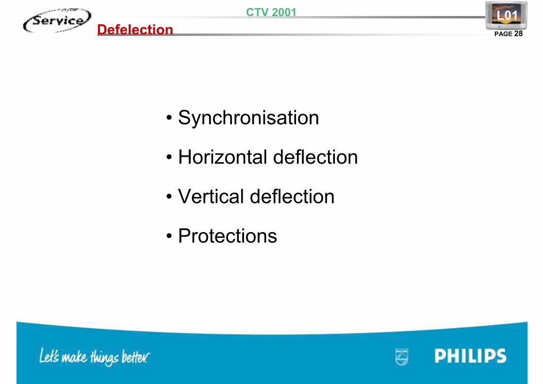
L01Defelection
• Synchronisation
• Horizontal deflection
• Vertical deflection
• Protections

CTV 2001
PAGE 29
L01Synchronisation
SYNC
Teletext
AcquisitionTeletext
/OSD
H-DriveH/V Sync
Separat. Horizontal
Deflection
VIDEO
SWITCH
H-DRIVE
H FLYBACK
EWdrive
EHTo
EHTInfo
V-Drive
EW
Vertical
Deflection
VDRA
VDRB
VH
V
H
UOC - Synchronisation
Internal CVBS
1
External
CVBS, SVHS or
Y/C
Vguard
TiltµPTILT
PANORAMA

CTV 2001
PAGE 30
L01

CTV 2001
PAGE 31
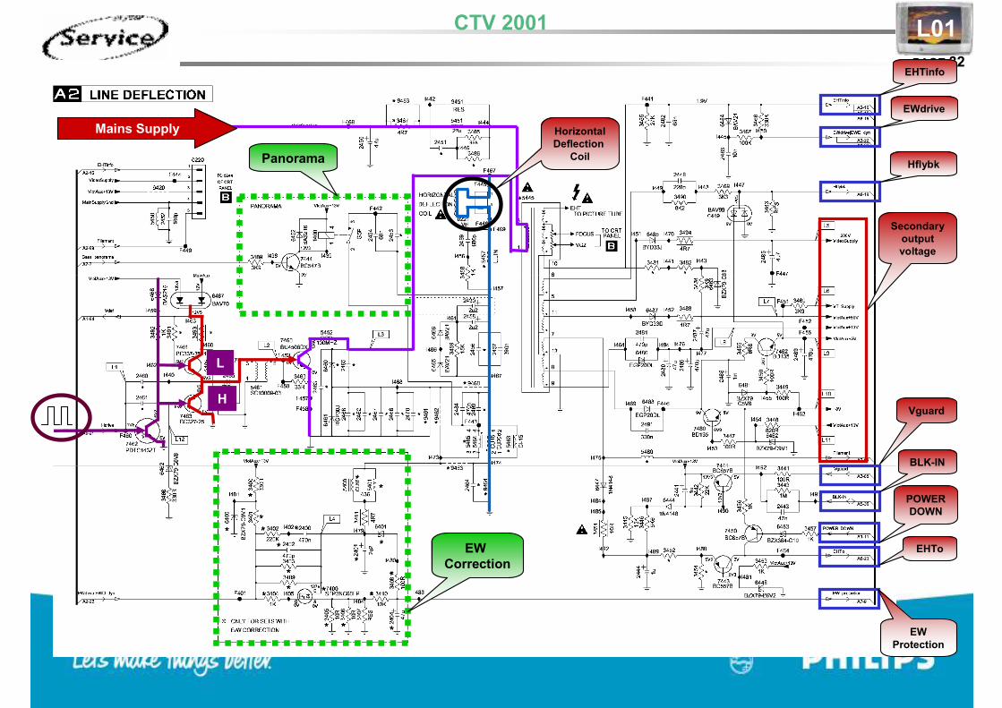
L01A2 Horizontal deflection
CTV 2001
PAGE 32
L01
H
L
EW
Correction
Panorama
Vguard
Secondary
output
voltage
EHTinfo
EWdrive
Hflybk
BLK-IN
POWER
DOWN
EW
Protection
EHTo
Mains Supply Horizontal
Deflection
Coil

CTV 2001
PAGE 33
L01EW correction

CTV 2001
PAGE 34
L01Auxiliary voltages LOT

CTV 2001
PAGE 35
L01A2 Auxiliary voltages

CTV 2001
PAGE 36
L01Panorama

CTV 2001
PAGE 37
L01A3 Frame deflection
Vdrive +
Vdrive -
Protection
Feedback

CTV 2001
PAGE 38
L01A2 Protections deflection H and V

CTV 2001
PAGE 39
L01BLK_IN/VGUARD Signal(UOC Pin 55)

CTV 2001
PAGE 40
L01
SERVICE MANUAL PAGE

CTV 2001
PAGE 41
L01Tips for debugging deflection
No. Problem symptom Check
1) Set cannot start-up &Vbatt volt not correct
Isolate 5561 & check Vbatt is correct now (PowerSupply ok) – check for 7460, 6460, 6461 failure.Check MainAux and VlotAux +13V (6467) arecorrect for base drive of deflection – check for7461, 7463 & 7460 failure.
2) Incorrect pic. width orEWProtection trigger
Isolate 5400 & check EW_protection is now nottrigger – check for 7400, 2401, 2404 failure.
3) No+200V,+50V,+13V,+8V,+5V supply
Check secundary voltage supply – 3494, 3488,6486, 7480, 7482.
4) Single horizontal line No vertical deflection – check 7471 Frame IC,VlotAux+13V failure.
5) Flyback line visible onscreen
Check 7330 Video amplifier, +200V supply failure.

CTV 2001
PAGE 42
L01
A6 Synchronisation
Iref Trame
Alim VP2Protection flash
Correction géométrie image
Protection Lignes OVP
switch off BT L et T

CTV 2001
PAGE 43
L01
Video Signal Processing
Video Signal Processing

CTV 2001
PAGE 44
L01
TDA955x/6x/7x/8x
General description
Combined the function of :
video processor + Micro-controller.
Basically divided in 4 main function :
1) Microcontroller
2) Video / Audio Demodulator
3) I/O Switching
4) SYNC Separator

CTV 2001
PAGE 45
L01

CTV 2001
PAGE 46
L01Tuner and IF QSS
Int CVBS
FM
Vision IF
Sound IF
SEL_IFPLL/Mtrap
I2C
QSS_AM_DEM_OUT
Tuner AGC
Tuner
Vision IF
QSS Sound IF
uP
IF Video output
Video
Processing
Sound
Trap
UOC Sound
Processing
Sound
Saw Filter
Visiion
Saw Filter

CTV 2001
PAGE 47
L01Tuner Block Diagram
UOC
IIC Data
Lines
TUNER
4/5
RF AGC
CIRCUIT
1 22
Video
SAW Filter
Audio
SAW Filter
71/72
18/19
23/24
SAW Filter
Switching Circuit
11
2
FM Input
SEL-IF-LL’

CTV 2001
PAGE 48
L01Video Processing
Radio
TV-Tuner
UOC
7200 - A
IF+ Ampl
UOC
7200 - C
Video
Processing
UOC
7200 - D
Synchronisation
.
I/O
Scart / Front
.

CTV 2001
PAGE 49
L01Tuner IF
Tuner
SAW
Video
SAW
SOUND
7002
7001
UOC Video
VIF1 = pin18
VIF2 = pin19
UOC Sound
SIF1 = pin23
SIF2 = pin24
SEL-IF-M-TRAP
FM RADIO
A5-24
10
11

CTV 2001
PAGE 50
L01
Schema service
manual
A4 page 26

CTV 2001
PAGE 51
L01Video processing
7200- A
Tuner
PIN18/19
IF VIDEO
IF SOUND
DemodulationAmpli
Video
49
38
EXT 1 CVBS
7200-C
CVBS
40
AGC
11

CTV 2001
PAGE 52
L01Video Processing
C-in
SY-CVBS-in
CVBS1-in
CVBS-terr-in
V-OUT CVBS vers Ext2
45
44
42
40
47
58
57
56
7200-C
51 52 53
R
V
B
EXT1 FBL
50
55
54
BLK-in
EHT-info
R
V
B
CTV 2001
PAGE 53
L01
Schema service manual
A5 page 27

CTV 2001
PAGE 54
L01Video source select
R Out
G Out
B Out
UOC
9/10/11
HEF4053BT
Scart 1 Video In
Scart 2 Video In
51
5
3
4
R In
G In
B In
52
53
42
44
Status 1
Status 2
FBL In 50
Front/Side Video In
Sound Trap
38
40
49
Scart 1 Video Out
Video Processing56
57
58
Scart 2 Video Out
47
21
BCL CircuitEHT Info
54
SEL-Main_Frnt_RR
RF Video
CTV 2001
PAGE 55
L01
Schema service manual
A10 page 32

CTV 2001
PAGE 56
L01B1 CRT panel
CTV 2001
PAGE 57
L01CRT
Schema service manual
B1 page 42

CTV 2001
PAGE 58
L012 CRT Scavem

CTV 2001
PAGE 59
L01Scavem
Schema service
manual
B2 page 43

CTV 2001
PAGE 60
L01
END
go back to
MAIN MENU
END
go back to
MAIN MENU

CTV 2001
PAGE 61
L01
MICROPROCESSOR

CTV 2001
PAGE 62
L01Micro Controller Diversity
TypeNumber
TeletextType
ROMSize
SoftwareUsed
Others
TDA9561 10 Page 128k 3EU1/3EU2 Inter-Carrier
TDA9567 10 Page 128k 3EU1 QSS
TDA9552 1 Page 64k 2EU0 QSS
TDA9551 1 Page 64k 2EU9 Inter-Carrier
TDA9550 1 Page 64k 2EU0 Inter-Carrier
TDA9572 Nil 32k 1EU0 QSS
TDA9571 Nil 32k 1EU0 Inter-Carrier
TDA9581 Nil 32k 1EU0 Inter-Carrier

CTV 2001
PAGE 63
L01Micro Controller block diagram
UOC
Micro Controller
NVM
ST24C16W6
IIC Data
Lines
MSP IC
TUNER
DEFLECTION
Horizontal
Pulse
Power SupplyStby_Con
Power Good
Keyboard/Protection
Vol/Mute/Treble/Bass/Panorama
Mono Audio Proc.
Audio Amp.
Source Select
Circuit
SEL-Main-Front-RR
SAW Filter
Switching
SEL-IF-LL’
ScartStatus 1/Status 2
Write Protect
Keyboard/Protection
Circuit
LED
IR
LED
IR
CTV 2001
PAGE 64
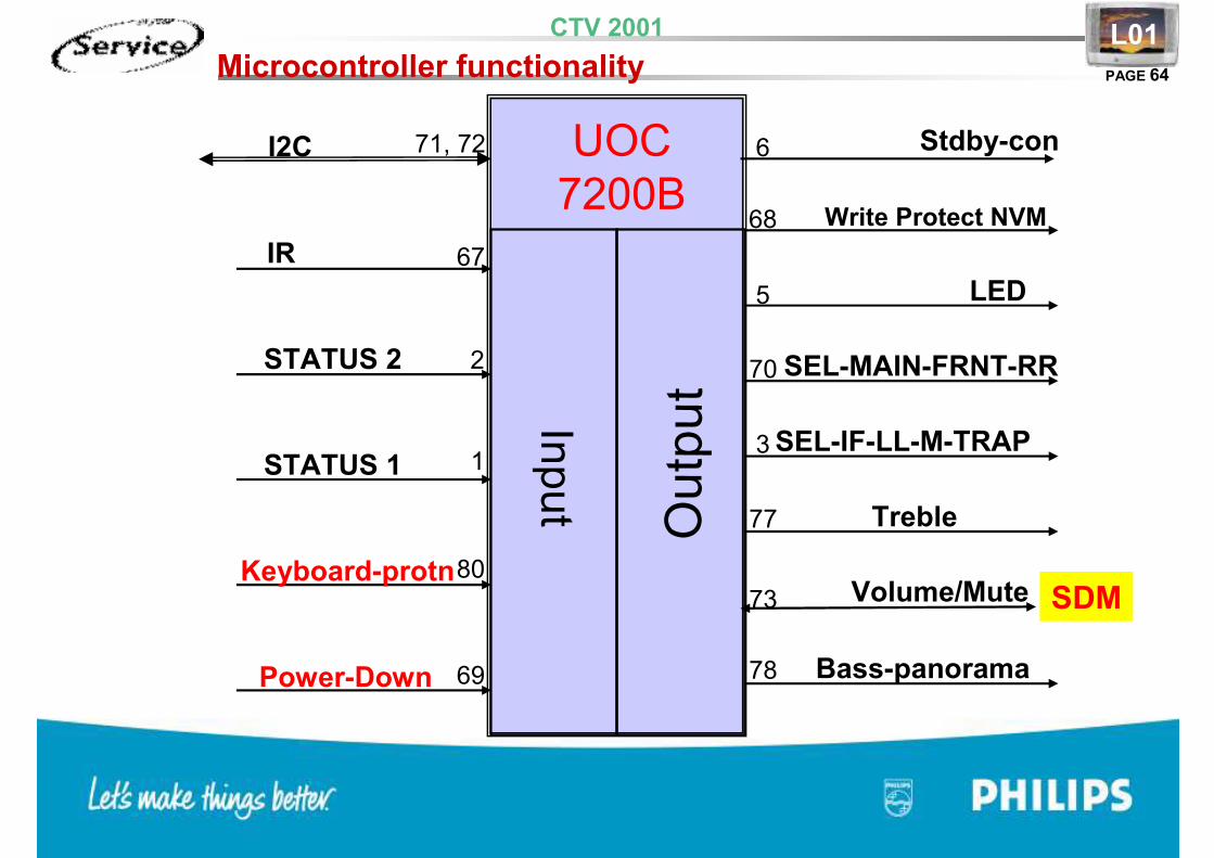
L01Microcontroller functionality
I2C Stdby-con
LED
SEL-MAIN-FRNT-RR
Volume/Mute
STATUS 2
Keyboard-protn
IR
Power-Down
STATUS 1SEL-IF-LL-M-TRAP
Bass-panorama
Treble
SDM
UOC
7200B
Input
Outp
ut
71, 72
67
2
1
80
69
6
5
70
3
77
73
78
Write Protect NVM68

CTV 2001
PAGE 65
L01Functionality TXT/OSD
CVBS Internal
H
V
R
V
B
BC Info/Protection
UOC
7200B
TXT OSD
56
57
58
31
40
55
SCART1
SCART2
42
4
4

CTV 2001
PAGE 66
L01UOC interface with power supply
POWER SUPPLY
BLOCK
WITH TEA 1507
CONTROL IC
UOC
+3.3 V
Power_down
Stdby_con
A. C. Mains
61
69
6
CTV 2001
PAGE 67
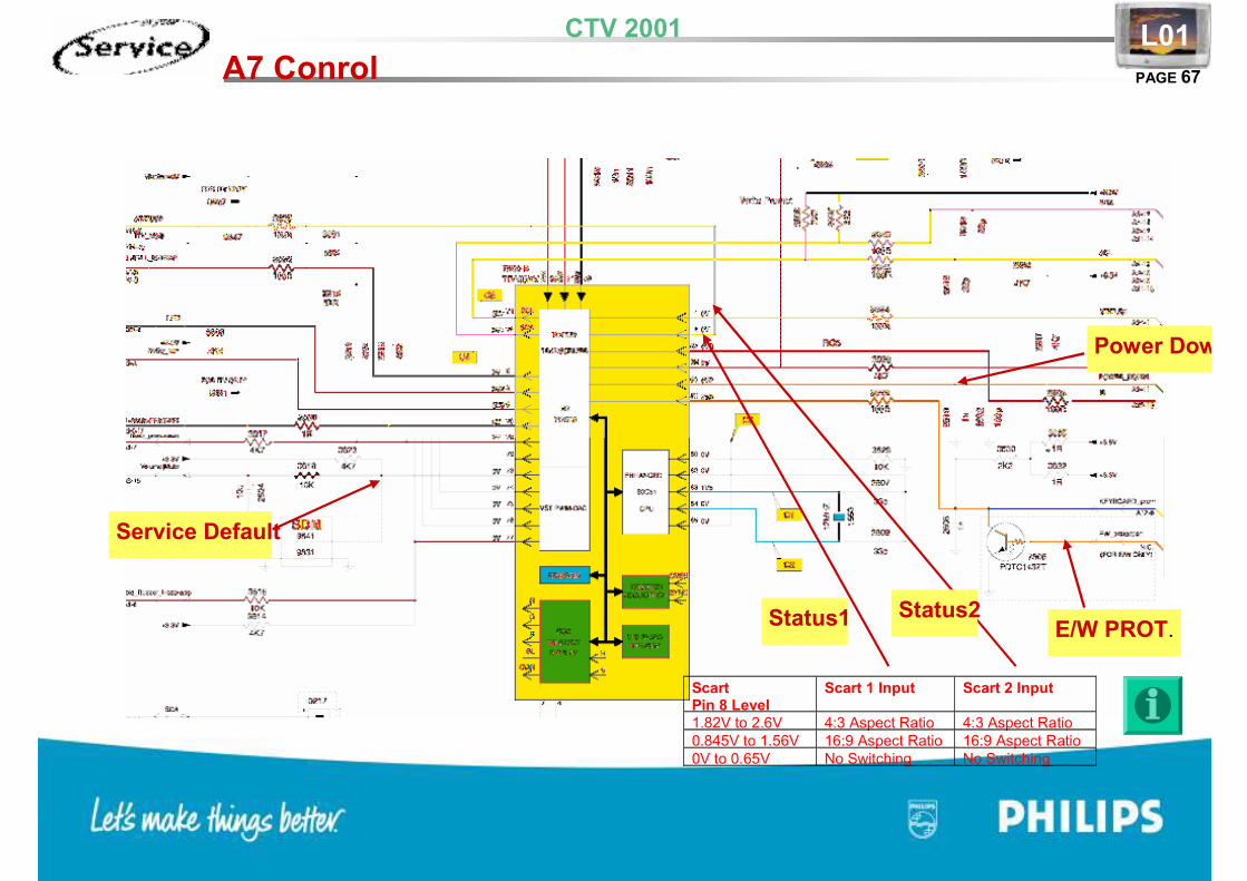
L01A7 Conrol
E/W PROT.
Service Default
ScartPin 8 Level
Scart 1 Input Scart 2 Input
1.82V to 2.6V 4:3 Aspect Ratio 4:3 Aspect Ratio
0.845V to 1.56V 16:9 Aspect Ratio 16:9 Aspect Ratio
0V to 0.65V No Switching No Switching
Status1 Status2
Power Down

CTV 2001
PAGE 68
L01Standby status UOC
Put Standby Con
To Low
Wait for 180ms
Enable
INTERRUPT
Put UOC out of
Standby
Set STB to high
Put STB to low
Wait for 550 ms
Put UOC in
standby
Disable interrupt
Put Standby Con
To High
PG LOW
Mute Audio
Put STB to low

CTV 2001
PAGE 69
L01Power ON-Standby-Power On-Power Off
Power ON
Power down
STB bit
Stdby_con
3.3V
Standby key press Out of Standby key press
Power offPower ONStandby
180ms
Interrupt status
Enable
Disable
UOC Status
Out of Stdby
Stdby
550ms
>3ms
Mute Audio Mute Audio

CTV 2001
PAGE 70
L01Power ON-Standby-Power OFF-Power ON
Power ON
Power down
STB bit
Stdby-con
3.3V
Standby key pressPower OFF Power ONStandby
Interrupt
status
Enable
Disable
UOC
status Stdby
Out of stdby
550ms
Mute Audio

CTV 2001
PAGE 71
L01Power ON - Fault condition
SEQUENCE OF OPERATIONS : POWER ON - FAULT CONDITION (OVER CURRENT BY V aux.)
Power ON
Power down
STB bit
Stdby-con
3.3V
Burst mode with
LOT shut downFault condition(Audio Over current)
Interruptstatus
Enable
Disable
UOC status Stdby
Out of stdby

CTV 2001
PAGE 72
L01Tips for debugging µP
1. Check that both +3.3V DC and +3.9V DC are present.
2. Check that crystal oscillator is working.
3. Check keyboard protection pin that it is in high logic. For sets with EW control,make sure that base of 7606 is low.
4. Check that Power Good signal is at high logic, normal operation.
5. Check that UOC is not in standby mode. Pin 6 of UOC should be 0V DC.
6. Make sure H-drive pulse is there. This can be check from resistor 3251. If H-drive is does not exist, remove resistor 3251 to check if there is loading.

CTV 2001
PAGE 73
L01
Schema service
manual
A7 page 29

CTV 2001
PAGE 74
L01
END
go back to
MAIN MENU
END
go back to
MAIN MENU

CTV 2001
PAGE 75
L01
AUDIO PROCESSING

CTV 2001
PAGE 76
L01Audio processing
TUNER
A4
UOC
A5
MSP
A9
Ampli
A8
Ext
Audio Ext
Audio
TUNER
A4
UOC
A5
Ampli
A8
SMART
AUDIO
A8
Ext
AudioExt
Audio
STEREO
MONO

CTV 2001
PAGE 77
L01A4 Sound IF
High for L’K9656M
K6289
K3953M

CTV 2001
PAGE 78
L01Audio Decoder/Processor
UOC
MSP
To Audio Amplifier
To Audio Amplifier
Mono
33
4818/19
47 24/25
23/24
From Tuner Output
Switch Circuit
From Tuner Output
(FM Radio)
TV SIF
(QSS)
38
Video with SIF
(Inter-Carrier)
VIF
SIF
Stereo
31
S.S
Note: S.S = Smart Sound

CTV 2001
PAGE 79
L01Mono sound processing
UOC - Audio Block
Demod + Source select + AVL
Volume control
Mono
Smart
Sound
Mono
Power
Amplifier
Ext IF (FMR)
Ext Audio 1
Ext Audio 2
CTV 2001
PAGE 80
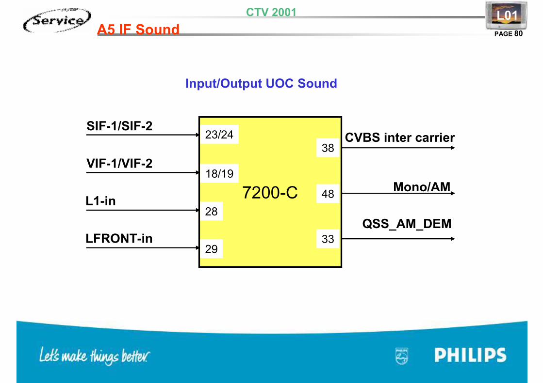
L01A5 IF Sound
7200-C
SIF-1/SIF-2
VIF-1/VIF-2
L1-in
LFRONT-in
CVBS inter carrier
Mono/AM
QSS_AM_DEM
23/24
18/19
28
29
38
48
33
Input/Output UOC Sound

CTV 2001
PAGE 81
L01A5 Sound mono set
Scart1 out mono
4211 for mono
Audio out mono

CTV 2001
PAGE 82
L01Nicam + 2CS + BTSC decoder
UOC
uPSound
IF
I2C
External Mono
Input
OSS_AM_DEM_OUT
External Stereo
Input
External
Audio
Output
SCART
DSP
Input
Select
Pre-
processingDemodulatorADC
DAC
DAC
Loudspeaker
Sound
Processing
PrescaleADC
Audio
Amplifier
SCART
Output
Select
Source
Select
L
R
L
R
L
R
Tuner SAW
Filter

CTV 2001
PAGE 83
L01Nicam + 2CS + BTSC Stereo Decoder
TV/RADIO
Select47
FMR
QSS-AM-DEM-OUT
Mono AM
SC1-Lin
SC1-Rin
3
Select Radio /TV
SC1-Lout
SC1-Rout
Main-OutL
Main-OutR
4
44
41
42
SC2 CTR
25
24
31
30
MSP34X5G

CTV 2001
PAGE 84
L01A9 Nicam +2CS + BTSC
Source select
Bandpass filterFM Radio
To Audio Ampl.
CTV 2001
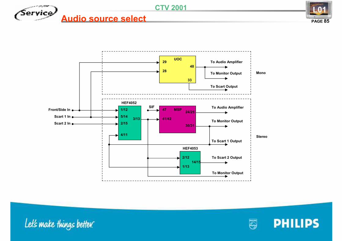
PAGE 85
L01Audio source select
UOC
MSP
HEF4052
To Audio Amplifier
To Monitor Output
To Monitor Output
To Audio Amplifier
Front/Side In
HEF4053
To Scart Output
To Scart 2 Output
To Scart 1 Output
Scart 1 In
Scart 2 In
Mono
Stereo
33
48
29
28
SIF47
41/42
24/25
30/31
1/12
5/14
2/15
4/11
3/13
2/12
1/13
14/15
To Monitor Output

CTV 2001
PAGE 86
L01A10 Audio/video source switching
Scart1 out Mono
To Micronas
to Scart 2 out
Monitor Out/AV
SC2_CTRL
SEL-Main-FRNT-RR

CTV 2001
PAGE 87
L01FM Radio
FM Radio Tuner
UOC
Micronas
Mono Amplifier
Stereo Amplifier

CTV 2001
PAGE 88
L01A9 FM Radio circuit
FM Radio Mono
FM Radio Stereo
BufferAmplifier
To Micronas

CTV 2001
PAGE 89
L01A8 Audio amplifier
AN7523 Headphone
Mono 1W - 3W
5
2/46
9
To Speaker
AN75226
Left Channel
Right Channel
Headphone
To Speaker
Mono 4W
Stereo 3W - 5W
5 9
8
2/4
10/12
Standby Mute/Vol
Standby Mute/Vol

CTV 2001
PAGE 90
L01Audio Output
Mono
Audio
Amplifier
UOC
uPVolume/mute
Sound
Processing
Mono System
AN7523

CTV 2001
PAGE 91
L01Audio Output
Sound
ProcessingStereo
Audio
Amplifier
UOC
uP
Main_OutR
Volume/mute
Main_OutL
R
L
Stereo System
AN7522N

CTV 2001
PAGE 92
L01A8 Audio amplifier
Processing
Audio
Mono
Amplifier
Stereo
Audio Processing
MSP ou
BTSC decoder
6
8
2/4
10/12
25
24
UOC
µP73
9
Amplifier
Mono
6
9
2/4
L
R
77 78
. .
Volume / Mute
2 x 5W
1 x 4W
BassTreble

CTV 2001
PAGE 93
L01
Schema service manual
A8 page 30

CTV 2001
PAGE 94
L01
END
go back to
MAIN MENU
END
go back to
MAIN MENU

CTV 2001
PAGE 95
L01
Error Code 0Error Code 0
A “0” in a buffer means an error has not been detected.
Contents of last 5 detected errors
L01US0 1.0 SDM
ERR 0 0 0 0 0

CTV 2001
PAGE 96
L01
99999 L011US1 1.0 SAM
ERR 0 0 0 0 0
XXX XXX XXX XXX XXX XXX XXX
Clear Clear?
Options
AKB 0
Tuner
White Tone
Geometry
Audio
S A M indication
OB(n) - Option Byte Value
Operation hours timer Software version
Contents of last 5 detected errors
Clear Error Buffer

CTV 2001
PAGE 97
L01
Item Description
IFPLL Default value = 24 (do not align)
AFW AFC w indow
AGC Default value = 28 (do not align)
SL On / O ff
YD Default value = 3 (do not align)
CL Default value = 4 (do not align)
AFA Not selectable
AFB Not selectable
Item Description
IFPLL Default value = 24 (do not align)
AFW AFC w indow
AGC Default value = 28 (do not align)
SL On / O ff
YD Default value = 3 (do not align)
CL Default value = 4 (do not align)
AFA Not selectable
AFB Not selectable

CTV 2001
PAGE 98
L01
Cool
Normal
Warm
DELTA COOL RED
DELTA COOL GREEN
DELTA COOL BLUE
NORMAL RED
NORMAL GREEN
NORMAL BLUE
DELTA WARM RED
DELTA WARM GREEN
DELTA WARM BLUE
White Tone

CTV 2001
PAGE 99
L01


