International Journal of Science and Research (IJSR) ISSN (Online): 2319-7064 Impact Factor (2012): 3.358 Volume 3 Issue 9, September 2014 www.ijsr.net Licensed Under Creative Commons Attribution CC BY Photo Voltic System Krishan Kumar 1 Mewar University, Department of Electrical Engineering, Chittorgarh, Rajasthan, India Abstract: This project proposes a novel dc to dc high step up chopper and good efficiency for photovoltaic renewable energy system in order to simplify the power system and their cost. The proposed power converter consists of a boost fused dc to dc converter added to cascaded H- bridge inverter circuit across the load. A proposed system includes three major units first is an operation type wherein power is delivered to dc chopper from solar photovoltaic (PV) cell, second is a single stage type design of dc to dc converter with high voltage gain to regulate the required output voltage and third for a closed loop control mechanism used to produce the good efficiency and control output for the system. Using MATLAB/Simulink the proposed scheme is developed. Keywords: MATLAB/Simulink, photovoltaic (PV) cell, boost converter, cascaded H- bridge inverter 1. Introduction The objective of this project is to propose a dc to dc boost power converter with high voltage gain using closed loop proportional integral and derivative control mechanism for renewable solar photovoltaic energy source. The proposed renewable power converter system has three advantages: i) power from the PV can be delivered to the utility load with expected values and without loss. ii) Maximum voltage and efficiency is realized by design of dc to dc converter and iii) a wide range of input irradiance and temperature is acceptable. The objective of this project is to propose a dc to dc high set up chopper and good efficiency for photovoltaic renewable energy system in order to simplify the power system and their cost. The proposed power converter consists of a boost fused dc to dc converter. A proposed system includes three major units: first is an operation type wherein power is delivered to dc chopper from solar photovoltaic (PV) renewable energy sources, second is a single stage type design of dc to dc converter with high voltage gain use to regulate the required output voltage and third for a closed loop control mechanism used to produce the good efficiency and control output for the system. The trapped solar energy is converted into DC voltage and the same is again converted into AC voltage using an Inverter and a load is connected to the output terminals of the inverter. 2. Photovoltaic System 2.1 Photovoltaic Effect Photovoltaic (PV) is a method of generating electrical power by converting solar radiation into direct current electricity using semiconductors that exhibit the photovoltaic effect. Photovoltaic power generation employs solar panels comprising a number of cells containing a photovoltaic material. Materials presently used for photovoltaic include mono crystalline silicon, polycrystalline silicon, amorphous silicon, cadmium telluride, and copper indium selenide/sulfide. Due to the growing demand for renewable energy sources, the manufacturing of solar cells and photovoltaic arrays has advanced considerably in recent years. The photovoltaic effect is the generation of a voltage (or a corresponding electric current) in a material upon exposure to light. Though the photovoltaic effect is directly related to the photoelectric effect, the two processes are different and should be distinguished. In the photoelectric effect, electrons are ejected from a material's surface upon exposure to radiation of sufficient energy. The photovoltaic effect is different in that the generated electrons are transferred between different bands (i.e. from the valence to conduction bands) within the material, resulting in the buildup of a voltage between two electrodes. Figure 1: PV effect converts the photon energy into voltage across the pn junction 2.1.1 Applications In Buildings In Transport Standalone Devices Rural Electrification Solar roadways Solar Power Satellites 2.2 Solar Cell A solar cell is a solid state device that converts the energy of sunlight directly into electricity by the photovoltaic effect. Assemblies of cells are used to make solar modules, also known as solar panels. The energy generated from these solar modules, referred to as solar power, is an example of solar energy Paper ID: SEP1414 1
Transcript
International Journal of Science and Research (IJSR) ISSN (Online): 2319-7064
Impact Factor (2012): 3.358
Volume 3 Issue 9, September 2014 www.ijsr.net
Licensed Under Creative Commons Attribution CC BY
Photo Voltic System
Krishan Kumar
1Mewar University, Department of Electrical Engineering, Chittorgarh, Rajasthan, India
Abstract: This project proposes a novel dc to dc high step up chopper and good efficiency for photovoltaic renewable energy system in order to simplify the power system and their cost. The proposed power converter consists of a boost fused dc to dc converter added to cascaded H- bridge inverter circuit across the load. A proposed system includes three major units first is an operation type wherein power is delivered to dc chopper from solar photovoltaic (PV) cell, second is a single stage type design of dc to dc converter with high voltage gain to regulate the required output voltage and third for a closed loop control mechanism used to produce the good efficiency and control output for the system. Using MATLAB/Simulink the proposed scheme is developed. Keywords: MATLAB/Simulink, photovoltaic (PV) cell, boost converter, cascaded H- bridge inverter
1. Introduction The objective of this project is to propose a dc to dc boost power converter with high voltage gain using closed loop proportional integral and derivative control mechanism for renewable solar photovoltaic energy source. The proposed renewable power converter system has three advantages: i) power from the PV can be delivered to the utility load with expected values and without loss. ii) Maximum voltage and efficiency is realized by design of dc to dc converter and iii) a wide range of input irradiance and temperature is acceptable. The objective of this project is to propose a dc to dc high set up chopper and good efficiency for photovoltaic renewable energy system in order to simplify the power system and their cost. The proposed power converter consists of a boost fused dc to dc converter.
A proposed system includes three major units: first is an operation type wherein power is delivered to dc chopper from solar photovoltaic (PV) renewable energy sources, second is a single stage type design of dc to dc converter with high voltage gain use to regulate the required output voltage and third for a closed loop control mechanism used to produce the good efficiency and control output for the system. The trapped solar energy is converted into DC voltage and the same is again converted into AC voltage using an Inverter and a load is connected to the output terminals of the inverter. 2. Photovoltaic System 2.1 Photovoltaic Effect Photovoltaic (PV) is a method of generating electrical power by converting solar radiation into direct current electricity using semiconductors that exhibit the photovoltaic effect. Photovoltaic power generation employs solar panels comprising a number of cells containing a photovoltaic material. Materials presently used for photovoltaic include mono crystalline silicon, polycrystalline silicon, amorphous silicon, cadmium telluride, and copper indium selenide/sulfide. Due to the growing demand for renewable energy sources, the manufacturing of solar cells and
photovoltaic arrays has advanced considerably in recent years. The photovoltaic effect is the generation of a voltage (or a corresponding electric current) in a material upon exposure to light. Though the photovoltaic effect is directly related to the photoelectric effect, the two processes are different and should be distinguished. In the photoelectric effect, electrons are ejected from a material's surface upon exposure to radiation of sufficient energy. The photovoltaic effect is different in that the generated electrons are transferred between different bands (i.e. from the valence to conduction bands) within the material, resulting in the buildup of a voltage between two electrodes.
Figure 1: PV effect converts the photon energy into voltage
across the pn junction 2.1.1 Applications In Buildings In Transport Standalone Devices Rural Electrification Solar roadways Solar Power Satellites 2.2 Solar Cell A solar cell is a solid state device that converts the energy of sunlight directly into electricity by the photovoltaic effect. Assemblies of cells are used to make solar modules, also known as solar panels. The energy generated from these solar modules, referred to as solar power, is an example of solar energy
Paper ID: SEP1414 1
International Journal of Science and Research (IJSR) ISSN (Online): 2319-7064
Impact Factor (2012): 3.358
Volume 3 Issue 9, September 2014 www.ijsr.net
Licensed Under Creative Commons Attribution CC BY
Figure 2: Basic construction of PV cell
2.2.1 Main Operation Solar cell works in three steps: Photons in sunlight hit the solar panel and are absorbed by semiconducting materials, such as silicon. Electrons (negatively charged) are knocked loose from their atoms, allowing them to flow through the material to produce electricity. Due to the special composition of solar cells, the electrons are only allowed to move in a single direction. An array of solar cells converts solar energy into a usable amount of direct current (DC) electricity. 2.2.2 Equivalent Circuit
Figure 3: PV cell equivalent circuit
2.2.3 Solar Panel A solar panel (photovoltaic module or photovoltaic panel) is a packaged interconnected assembly of solar cells, also known as photovoltaic cells. The solar panel can be used as a component of a larger photovoltaic system to generate and supply electricity in commercial and residential applications.
Figure 4: Solar Panel System
2.2.4 Working Solar panels use light energy (photons) from the sun to generate electricity through the photovoltaic effect. The structural (load carrying) member of a module can either be the top layer (superstreet) or the back layer (substrate). The majority of modules use wafer-based crystalline silicon cells or thin-film cells based on cadmium telluride or silicon. The p-n junctions of mono-crystalline silicon cells may have adequate reverse current characteristics that these are not necessary. Reverse currents are not only inefficient as they represent power losses, but they can also lead to problematic heating of shaded cells. Solar cells become less efficient at higher temperatures and so it desirable to minimize heat in the panels. Very few modules incorporate any design features to decrease temperature, but installers try to provide good ventilation behind solar panels. 2.2.5 Major Components of a Solar Panel Glass Cover- Provides protection from the elements .Anti-Reflective Coating – Substance used to prevent the light that strikes from bouncing off the panel. .Top Negative Contact - Negative Post (Terminal, like in your battery) .N-Type Layer - Semi-conductor layer dipped in phosphorus .P-Type Layer - Semi-conductor layer dipped in boron .Bottom Positive Contact - Positive Post (Terminal, like in a battery). 2.3 Working Factors of PV Array
Sun Intensity Sun Angle Shadow Effect Temperature Effects 2.4 Types of Photovoltaic Systems
1) Stand-alone systems 2) Hybrid systems 3) Grid-connected or utility-interactive systems
Paper ID: SEP1414 2
International Journal of Science and Research (IJSR) ISSN (Online): 2319-7064
Impact Factor (2012): 3.358
Volume 3 Issue 9, September 2014 www.ijsr.net
Licensed Under Creative Commons Attribution CC BY
3. Boost Converter 3.1 Introduction A boost converter (step-up converter) is a DC-to-DC power converter with an output voltage greater than its input voltage. It is a class of switched-mode power supply (SMPS) containing at least two semiconductor switches (a diode and a transistor) and at least one energy storage element, a capacitor, inductor, or the two in combination. Filters made of capacitors (sometimes in combination with inductors) are normally added to the output of the converter to reduce output voltage ripple.
Power for the boost converter can come from any suitable DC sources, such as batteries, solar panels, rectifiers and DC generators. A process that changes one DC voltage to a different DC voltage is called DC to DC conversion. A boost converter is a converter with an output voltage greater than the source voltage.
A boost converter is sometimes called a step-up converter since it “steps up” the source voltage. Since power (
) must be conserved, the output current is lower than the source current.
Figure 5: The block diagram of a boost converte
3.2 Continuous Mode 3.3 Discontinuous Mode 3.3 PI Controller
A PI Controller (proportional-integral controller) is a special case of the PID controller in which the derivative (D) of the error is not used. The controller output is given by
KP +KI
Where is the error or deviation of actual measured value (PV) from the setpoint (SP)
A PI controller can be modeled easily in software such as Simulink or Xcos using a “flow chart” box
involving Laplace operator:
C=
Where
Proportional gain G = KP
= KI = integral gain
Setting a value for is often a tradeoff between decreasing overshoot and increasing settling time. The lack of derivative action may make the system more Steady in the steady state in the case of noisy data. This is because derivative action is more sensitive to higher-frequency terms in the inputs. Without derivative action, a PI-controlled system is less responsive to real (non-noise) and relatively fast alterations in state and so the system will be slower to reach setpoint and slower to respond to perturbations than a well-tuned PID system may be. Derivative Of The Process Variable Set Point Ramping Set Point Weighting
Figure 6: Basic block of a PI controller
3.4 Need for MPPT Photovoltaic (PV) offers an environmentally friendly source of electricity, of which the fuel is sunshine, a renewable energy. To date, this way of electricity generation, however, has been relatively costly. Very often, the success of a PV application depends on whether the power electronics device can extract sufficiently high power from the PV arrays to keep overall output power per unit cost low. The maximum power point tracking (MPPT) of the PV output for all sunshine conditions, therefore, becomes a key control in the device operation for successful PV applications. The MPPT control is, in general, challenging, because the sunshine condition that determines the amount of sun energy into the PV array may change all the time, and the current voltage characteristic of PV arrays is highly nonlinear. A PV system for the grid-connected applications is typically composed of five main components: 1) a PV array that converts solar energy to electric energy 2) a dc-dc converter that converts one dc voltages produced by the PV arrays to another dc voltage which charges a battery 3) an inverter that converts the high dc voltage to a single- or three-phase ac voltage 4) a digital controller that controls the converter operation with MPPT capability 5) a ac filter that absorbs voltage/current harmonics generated by the inverter. block diagram of photovoltaic power system A PV system
for the grid-connected applications is typically
Paper ID: SEP1414 3
International Journal of Science and Research (IJSR) ISSN (Online): 2319-7064
Impact Factor (2012): 3.358
Volume 3 Issue 9, September 2014 www.ijsr.net
Licensed Under Creative Commons Attribution CC BY
Figure 7: block diagram of photovoltaic power system
A PV system for the grid-connected applications is typically composed of five main components: 1) a PV array that converts solar energy to electric energy 2) a dc-dc converter that converts one dc voltages produced by the PV arrays to another dc voltage which charges a battery 3) an inverter that converts the high dc voltage to a single- or three-phase ac voltage 4) a digital controller that controls the converter operation with MPPT capability 5) a ac filter that absorbs voltage/current harmonics generated by the inverter. 4. Introduction to Inverters 4.1 Classification of Inverter (a) Classification according to the Nature of Input Source
Voltage Source Inverters(VSI) Current Source Inverters(CSI)
(b)Classification according to the Wave shape of the Output voltage
4.2 Multilevel Inverters Recent advances in the power-handling capabilities of static switch devices such as IGBTs with voltage rating up to 4.5 kV commercially available, has made the use of the voltage source inverters (VSI) feasible for high-power applications. High power and high-voltage conversion systems have become very important issues for the power electronic industry handling the large ac drive and electrical power applications at both the transmission and distribution levels. For these reasons, a new family of multilevel inverters has emerged as the solution for working with higher voltage levels. Multilevel inverters include an array of power semiconductors and capacitor voltage sources, the output of which generate voltages with stepped waveforms. 4.3 Classification of Multilevel Inverters 4.3.1 Cascaded H-Bridge Multilevel Inverter This new inverter can avoid extra clamping diodes or voltage balancing capacitors. Again, the cascaded multilevel inverters are classified depending the type of DC sources used throughout the input. A single-phase structure of an m-level cascaded inverter is Each separate dc source (SDCS) is connected to a single-phase full-bridge, or H-bridge, inverter. Each inverter level can generate three different voltage outputs, +Vdc, 0, and –Vdc by connecting the dc source to the ac output by different combinations of the four switches, S1, S2, S3, and S4. To obtain +Vdc, switches S1 and S4 are turned on, whereas –Vdc can be obtained by turning on switches S2 and S3. By turning on S1 and S2 or S3 and S4, the output voltage is 0. The ac outputs of each of the different full-bridge inverter levels are connected in series such that the synthesized voltage waveform is the sum of the inverter outputs.
Figure 8: Single phase structures of Cascaded inverter (a) 3-level, (b)5-level, (c) 7-level
Paper ID: SEP1414 4
International Journal of Science and Research (IJSR) ISSN (Online): 2319-7064
Impact Factor (2012): 3.358
Volume 3 Issue 9, September 2014 www.ijsr.net
Licensed Under Creative Commons Attribution CC BY
4.3.2 Symmetrical Cascaded H-Bridge multilevel Inverter If all the input sources are of equal magnitude, it is known as Symmetrical H-Bridge inverter as shown in fig 3.6.1 and the switching sequence is given in table 3 .Here both the full bridge inverters are fed with different sources of equal magnitude.
Figure 9: Symmetrical five level Cascaded H-Birdge
inverter 4.3.3 Asymmetrical Cascaded H-Bridge multilevel Inverter The cascaded H-Bridge multilevel inverter with two SDCS with unequal magnitude is known as Asymmetrical Cascaded H-Bridge multilevel Inverter. The following is figure 2.17 of Asymmetrical Cascaded H-Bridge multilevel Inverter where it is having 2 unequal DC sources +2Vdc/3 and +Vdc/3.
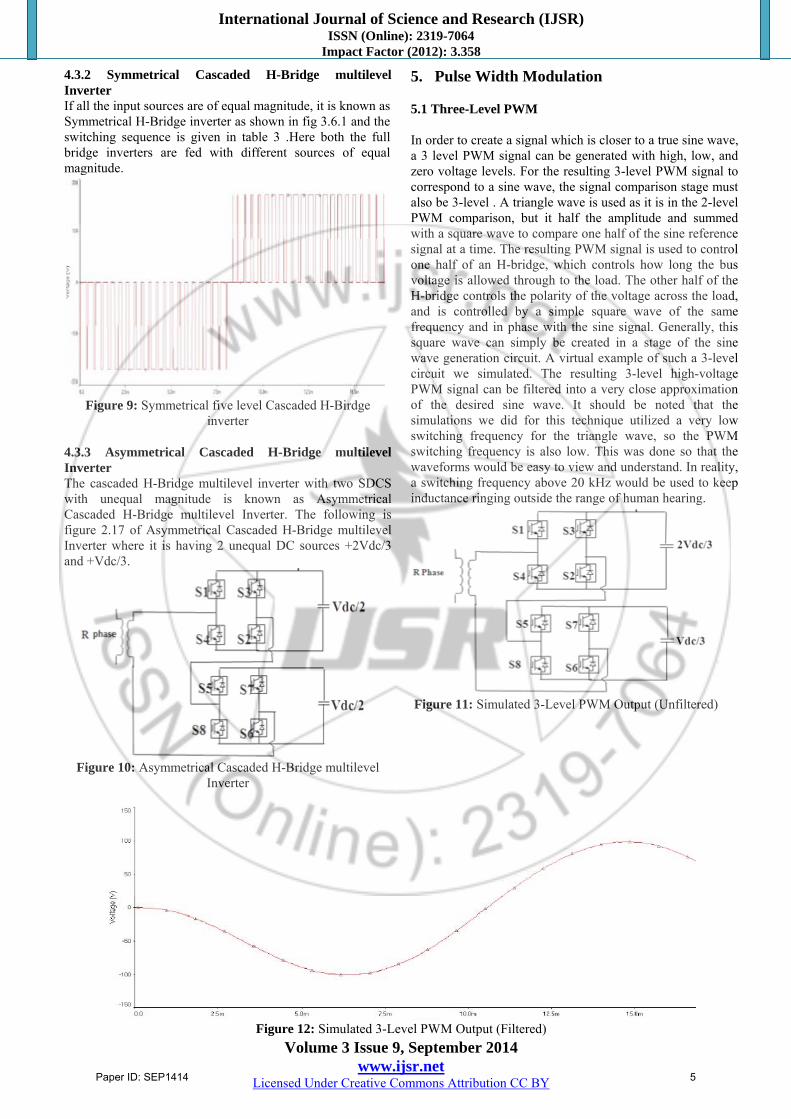
5. Pulse Width Modulation 5.1 Three-Level PWM In order to create a signal which is closer to a true sine wave, a 3 level PWM signal can be generated with high, low, and zero voltage levels. For the resulting 3-level PWM signal to correspond to a sine wave, the signal comparison stage must also be 3-level . A triangle wave is used as it is in the 2-level PWM comparison, but it half the amplitude and summed with a square wave to compare one half of the sine reference signal at a time. The resulting PWM signal is used to control one half of an H-bridge, which controls how long the bus voltage is allowed through to the load. The other half of the H-bridge controls the polarity of the voltage across the load, and is controlled by a simple square wave of the same frequency and in phase with the sine signal. Generally, this square wave can simply be created in a stage of the sine wave generation circuit. A virtual example of such a 3-level circuit we simulated. The resulting 3-level high-voltage PWM signal can be filtered into a very close approximation of the desired sine wave. It should be noted that the simulations we did for this technique utilized a very low switching frequency for the triangle wave, so the PWM switching frequency is also low. This was done so that the waveforms would be easy to view and understand. In reality, a switching frequency above 20 kHz would be used to keep inductance ringing outside the range of human hearing.
International Journal of Science and Research (IJSR) ISSN (Online): 2319-7064
Impact Factor (2012): 3.358
Volume 3 Issue 9, September 2014 www.ijsr.net
Licensed Under Creative Commons Attribution CC BY
The 3-Level PWM frequency plot shown in figure 4.8 markedly improved over those of the square and modified sine techniques. The primary frequency of 60Hz is the dominant in all three, but the magnitude of the harmonic frequencies is much reduced in 3-Level PWM, and the primary is of larger magnitude. When compared to the 2-level PWM, however, a couple things are noticed. First, the harmonics plot shows no higher level harmonics of significant magnitude. This represents the 3-Level signal following much more closely the desired sine wave. However, the primary frequency has a much lower voltage magnitude than that of the 2-Level design. The reason for this is the presence of other frequencies which are not harmonics of the 60Hz signal, which are caused by the switching of the signal from one polarity to the other, and back. 6. Simulation Results 6.1 Simulink Model of Proposed System with Three Level Inverter
Figure 13: Simulink model
6.2 Simulation Output waveforms
Figure 14: Without filter in 3-level inverter
6.2.1 Without filter condition
Figure 15: Total harmonic distraction without filter
6.2.2 With filter condition:
Figure 16: With filter in 3-level inverter
Figure 17: Total harmonic distraction with filter
Paper ID: SEP1414 6
International Journal of Science and Research (IJSR) ISSN (Online): 2319-7064
Impact Factor (2012): 3.358
Volume 3 Issue 9, September 2014 www.ijsr.net
Licensed Under Creative Commons Attribution CC BY
7. Conclusion
A creative DC to DC boost power converter with high voltage gain output using closed loop proportional integral and derivative control mechanism for solar photovoltaic renewable energy system is proposed. It has the following advantages: 1) power from the PV module can be delivered to the utility load directly without transmission loss. 2) The proposed system is realized high voltage and high efficiency. a large range of input voltage variation caused by different isolation and temperature are made acceptable. In this Project, the operation principle of the proposed dc to dc boost power converter has been introduced using closed loop control mechanism is adopted to realize the maximum power and voltage output of the circuit. The trapped solar energy is converted into DC voltage and the same is again converted into AC voltage using an Inverter and connected to the load. The control circuits are simulated by using MATLAB/Simulink Simulation results at different operating conditions and are shown. References [1] A betka, A moussi, “Performance optimization of a
photovoltaic induction motor pumping system” [2] B. Bai, C. Mi, and S. Gargies, “The short-time-scale
transient processes in high-voltage and high power isolated bidirectional DC-DC converters,” IEEE Trans. Power Electron.
[3] DarigaMeekhun, Vincent Boitier, Jean-Marie Dilhac,et.tell, “Buck converter design for Photovoltaic generators with super capacitor energy storage”, International Conference on Renewable Energies and Power Quality (ICREPQ‟11) Las Palmas de Gran Canaria (Spain).
[4] Dave Freeman,” Introduction to Photovoltaic Systems Maximum Power Point Tracking”,Texas instruments, Application Report.
[5] Ishaque K, Salam Z, Syafaruddin, “A comprehensive MATLAB Simulink PV system simulator with partial shading capability based on two-diode model”,Solar Energy.
[6] Ishaque K, Salam Z, Taheri H, “Accurate MATLAB simulink PV system simulator based on a two-diode model”
[7] Jeremy Lagorse,DamienPaire,AbdellatifMiraoui,”Sizing optimization of a stand-alone street lighting system powered by a hybrid system using fuel cell, PV and battery”,Elsevierltd,Renewable Energy.
[8] Johan H. R. Enslin, Mario S. Wolf, Dani¨el B. Snyman, and WernherSwiegers,” Integrated Photovoltaic Maximum Power Point Tracking Converter”, IEEE Transactions on Industrial Electronics.
[9] Mohamed Azab,” A New Maximum Power Point Tracking for Photovoltaic Systems”, International Journal of Electrical and Electronics Engineering.
[10] N. AmmasaiGounden, Sabitha Ann Peter, HimajaNallandula, S. Krithiga, “Fuzzy logic controller with MPPT using line-commutated inverter for three-phase grid-connected photovoltaic systems”, Renewable Energy(Elsevier).
Author Profile
Krishan Kumar is from Mewar University, Department of Electrical Engineering, Chittorgarh, Rajasthan, India