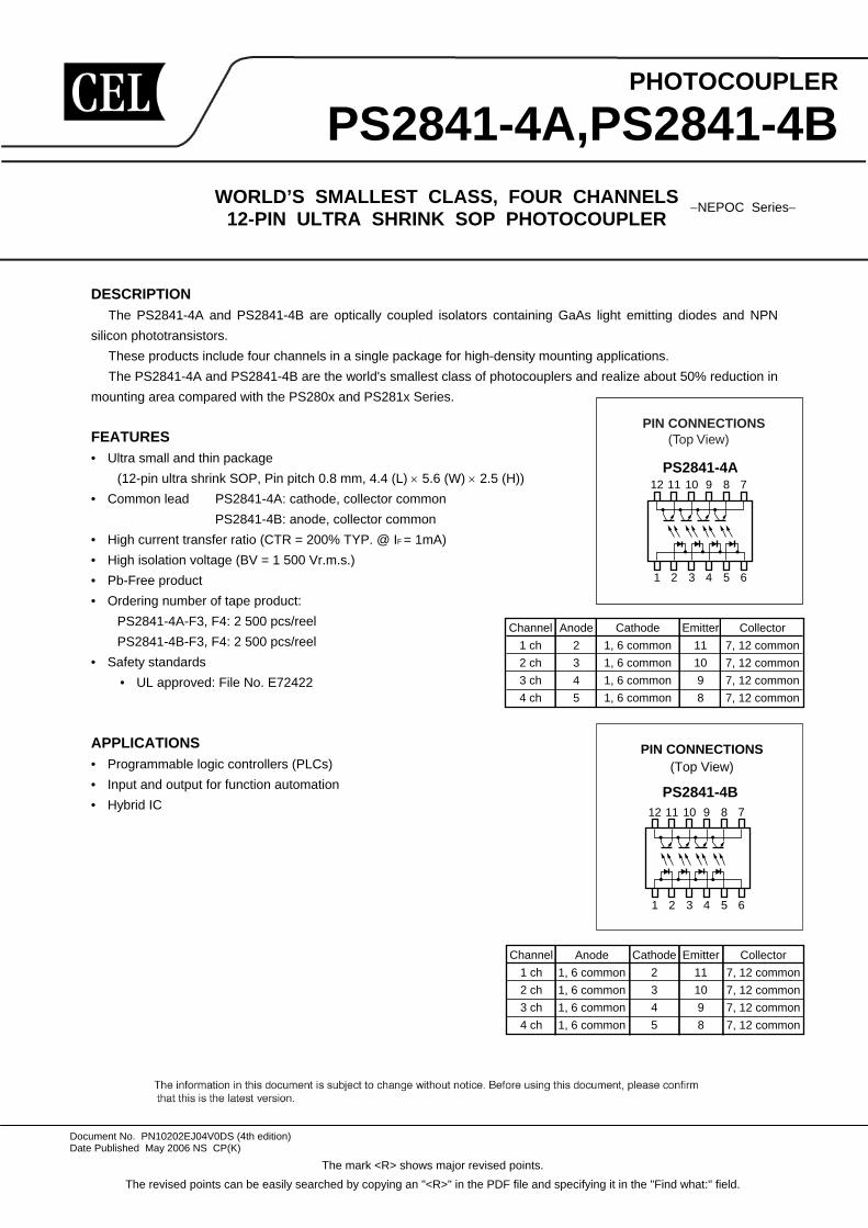
The mark <R> shows major revised points. The revised points can be easily searched by copying an "<R>" in the PDF file and specifying it in the "Find what:" field. PHOTOCOUPLER PS2841-4A,PS2841-4B WORLD’S SMALLEST CLASS, FOUR CHANNELS 12-PIN ULTRA SHRINK SOP PHOTOCOUPLER −NEPOC Series− Document No. PN10202EJ04V0DS (4th edition) Date Published May 2006 NS CP(K) DESCRIPTION The PS2841-4A and PS2841-4B are optically coupled isolators containing GaAs light emitting diodes and NPN silicon phototransistors. These products include four channels in a single package for high-density mounting applications. The PS2841-4A and PS2841-4B are the world's smallest class of photocouplers and realize about 50% reduction in mounting area compared with the PS280x and PS281x Series. FEATURES • Ultra small and thin package (12-pin ultra shrink SOP, Pin pitch 0.8 mm, 4.4 (L) × 5.6 (W) × 2.5 (H)) • Common lead PS2841-4A: cathode, collector common PS2841-4B: anode, collector common • High current transfer ratio (CTR = 200% TYP. @ IF = 1mA) • High isolation voltage (BV = 1 500 Vr.m.s.) • Pb-Free product • Ordering number of tape product: PS2841-4A-F3, F4: 2 500 pcs/reel PS2841-4B-F3, F4: 2 500 pcs/reel • Safety standards • UL approved: File No. E72422 APPLICATIONS • Programmable logic controllers (PLCs) • Input and output for function automation • Hybrid IC 1 2 3 4 5 6 12 11 10 9 8 7 PS2841-4A Channel 1 ch 2 ch 3 ch 4 ch Anode 2 3 4 5 Cathode 1, 6 common 1, 6 common 1, 6 common 1, 6 common Emitter 11 10 9 8 Collector 7, 12 common 7, 12 common 7, 12 common 7, 12 common PIN CONNECTIONS (Top View) 1 2 3 4 5 6 12 11 10 9 8 7 PS2841-4B PIN CONNECTIONS (Top View) Channel 1 ch 2 ch 3 ch 4 ch Anode 1, 6 common 1, 6 common 1, 6 common 1, 6 common Cathode 2 3 4 5 Emitter 11 10 9 8 Collector 7, 12 common 7, 12 common 7, 12 common 7, 12 common
Transcript
The mark <R> shows major revised points. The revised points can be easily searched by copying an "<R>" in the PDF file and specifying it in the "Find what:" field.
PHOTOCOUPLER
PS2841-4A,PS2841-4BWORLD’S SMALLEST CLASS, FOUR CHANNELS
Document No. PN10202EJ04V0DS (4th edition) Date Published May 2006 NS CP(K)
DESCRIPTION The PS2841-4A and PS2841-4B are optically coupled isolators containing GaAs light emitting diodes and NPN
silicon phototransistors. These products include four channels in a single package for high-density mounting applications. The PS2841-4A and PS2841-4B are the world's smallest class of photocouplers and realize about 50% reduction in
mounting area compared with the PS280x and PS281x Series.
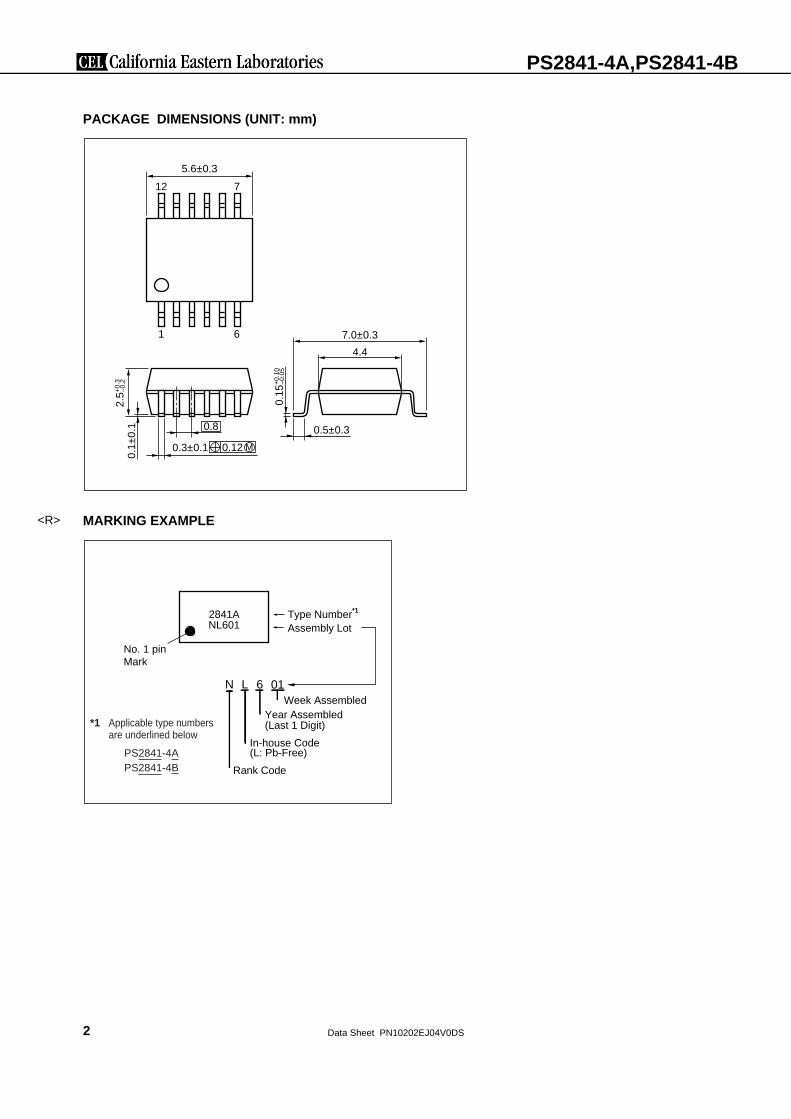
FEATURES • Ultra small and thin package
(12-pin ultra shrink SOP, Pin pitch 0.8 mm, 4.4 (L) × 5.6 (W) × 2.5 (H))• Common lead PS2841-4A: cathode, collector common
PS2841-4B: anode, collector common • High current transfer ratio (CTR = 200% TYP. @ IF = 1mA)• High isolation voltage (BV = 1 500 Vr.m.s.)• Pb-Free product• Ordering number of tape product:
*1 For the application of the Safety Standard, following part number should be used.
ABSOLUTE MAXIMUM RATINGS (TA = 25°C, unless otherwise specified)
Parameter Symbol Ratings Unit
Diode Forward Current (DC) IF 20 mA/ch
Reverse Voltage VR 6 V
Power Dissipation Derating ∆ IF /°C 0.2 mA /°C
Peak Forward Current *1 IFP 0.5 A/ch
Transistor Collector to Emitter Voltage VCEO 70 V
Emitter to Collector Voltage VECO 5 V
Collector Current IC 20 mA/ch
Power Dissipation Derating ∆PC/°C 0.4 mW/°C
Power Dissipation PC 40 mW/ch
Isolation Voltage *2 BV 1 500 Vr.m.s.
Operating Ambient Temperature TA –40 to +100 °C
Storage Temperature Tstg –55 to +125 °C
*1 PW = 100 µs, Duty Cycle = 1%*2 AC voltage for 1 minute at TA = 25°C, RH = 60% between input and output.
Pins 1-6 shorted together, 7-12 shorted together.
<R>
Data Sheet PN10202EJ04V0DS 4
PS2841-4A,PS2841-4B
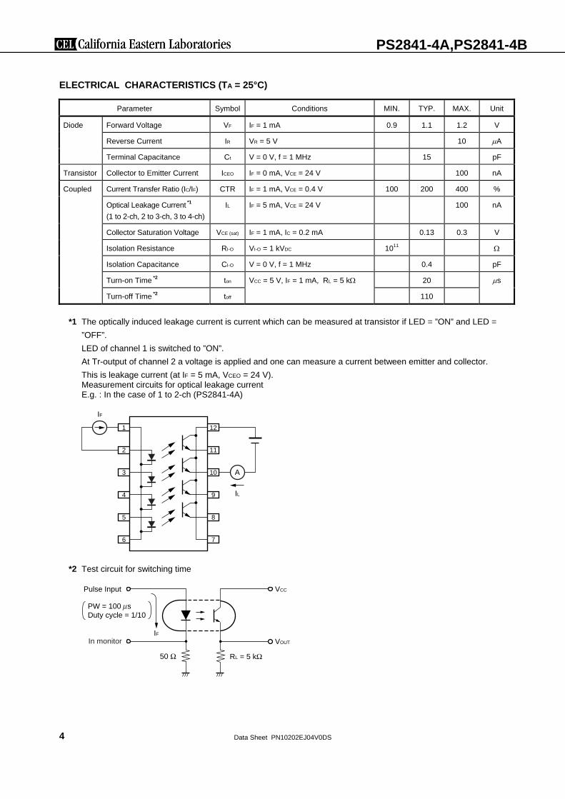
ELECTRICAL CHARACTERISTICS (TA = 25°C)
Parameter Symbol Conditions MIN. TYP. MAX. Unit
Diode Forward Voltage VF IF = 1 mA 0.9 1.1 1.2 V
Reverse Current IR VR = 5 V 10 µA
Terminal Capacitance Ct V = 0 V, f = 1 MHz 15 pF
Transistor Collector to Emitter Current ICEO IF = 0 mA, VCE = 24 V 100 nA
Coupled Current Transfer Ratio (IC/IF) CTR IF = 1 mA, VCE = 0.4 V 100 200 400 %
Optical Leakage Current *1 (1 to 2-ch, 2 to 3-ch, 3 to 4-ch)
IL IF = 5 mA, VCE = 24 V 100 nA
Collector Saturation Voltage VCE (sat) IF = 1 mA, IC = 0.2 mA 0.13 0.3 V
Isolation Resistance RI-O VI-O = 1 kVDC 1011 Ω
Isolation Capacitance CI-O V = 0 V, f = 1 MHz 0.4 pF
Turn-on Time *2 ton VCC = 5 V, IF = 1 mA, RL = 5 kΩ 20 µs
Turn-off Time *2 toff 110
*1 The optically induced leakage current is current which can be measured at transistor if LED = ”ON” and LED =”OFF”. LED of channel 1 is switched to ”ON”. At Tr-output of channel 2 a voltage is applied and one can measure a current between emitter and collector. This is leakage current (at IF = 5 mA, VCEO = 24 V). Measurement circuits for optical leakage current E.g. : In the case of 1 to 2-ch (PS2841-4A)
• Peak reflow temperature 260°C or below (package surface temperature) • Time of peak reflow temperature 10 seconds or less • Time of temperature higher than 220°C 60 seconds or less • Time to preheat temperature from 120 to 180°C 120±30 s• Number of reflows Three • Flux Rosin flux containing small amount of chlorine (The flux with a
maximum chlorine content of 0.2 Wt% is recommended.)
120±30 s(preheating)
220˚C
180˚C
Pac
kage
Sur
face
Tem
pera
ture
T (
˚C)
Time (s)
Recommended Temperature Profile of Infrared Reflow
(heating)to 10 s
to 60 s
260˚C MAX.
120˚C
(2) Wave soldering• Temperature 260°C or below (molten solder temperature) • Time 10 seconds or less • Preheating conditions 120°C or below (package surface temperature)• Number of times One (Allowed to be dipped in solder including plastic mold portion.) • Flux Rosin flux containing small amount of chlorine (The flux with a maximum chlorine
content of 0.2 Wt% is recommended.)
(3) Soldering by soldering iron• Peak temperature (lead part temperature) 350°C or below• Time (each pins) 3 seconds or less • Flux Rosin flux containing small amount of chlorine (The flux with a
maximum chlorine content of 0.2 Wt% is recommended.)
(a) Soldering of leads should be made at the point 1.5 to 2.0 mm from the root of the lead.(b) Please be sure that the temperature of the package would not be heated over 100°C.
Data Sheet PN10202EJ04V0DS 10
PS2841-4A,PS2841-4B
(4) Cautions• Fluxes
Avoid removing the residual flux with freon-based and chlorine-based cleaning solvent.
2. Cautions regarding noiseBe aware that when voltage is applied suddenly between the photocoupler’s input and output or between
collector-emitters at startup, the output transistor may enter the on state, even if the voltage is within the absolutemaximum ratings.
3. Measurement conditions of current transfer ratios (CTR), which differ according to photocouplerCheck the setting values before use, since the forward current conditions at CTR measurement differ according
to product.When using products other than at the specified forward current, the characteristics curves may differ from the
standard curves due to CTR value variations or the like. Therefore, check the characteristics under the actual operating conditions and thoroughly take variations or the like into consideration before use.
USAGE CAUTIONS 1. Protect against static electricity when handling.2. Avoid storage at a high temperature and high humidity.
<R>
0604
PS2841-4A,PS2841-4B
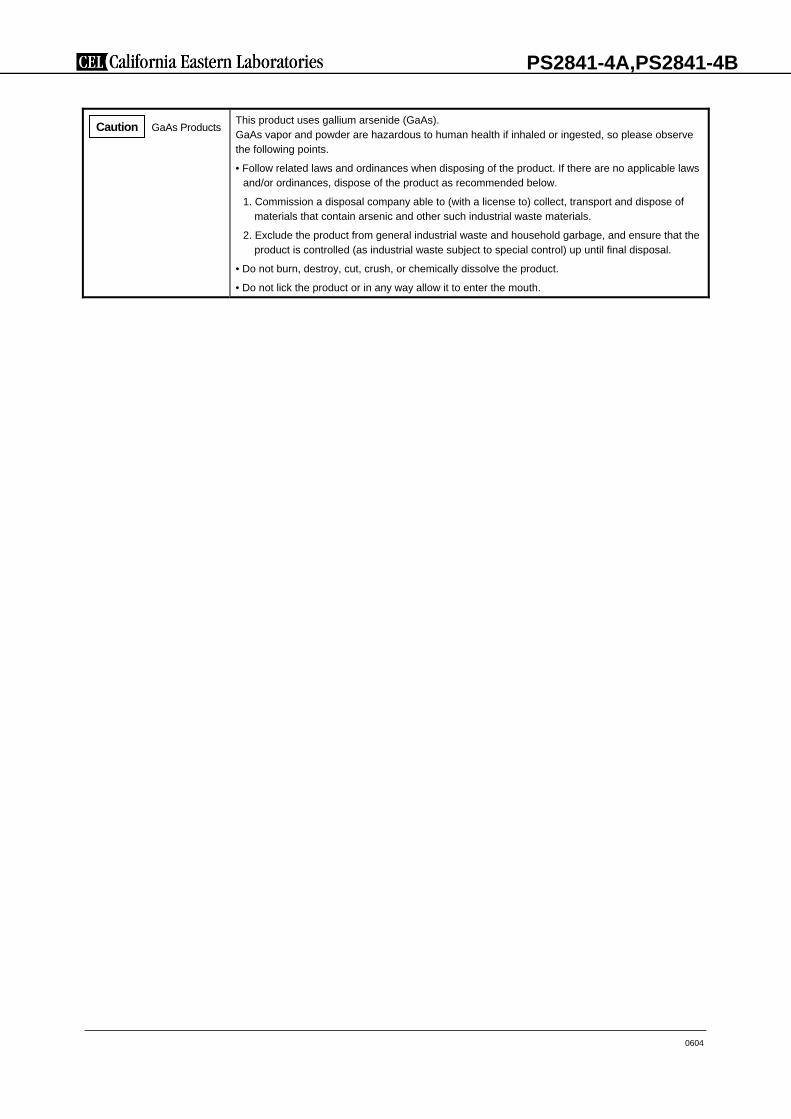
Caution GaAs Products This product uses gallium arsenide (GaAs). GaAs vapor and powder are hazardous to human health if inhaled or ingested, so please observe the following points.
• Follow related laws and ordinances when disposing of the product. If there are no applicable lawsand/or ordinances, dispose of the product as recommended below.
1. Commission a disposal company able to (with a license to) collect, transport and dispose ofmaterials that contain arsenic and other such industrial waste materials.
2. Exclude the product from general industrial waste and household garbage, and ensure that theproduct is controlled (as industrial waste subject to special control) up until final disposal.
• Do not burn, destroy, cut, crush, or chemically dissolve the product.
• Do not lick the product or in any way allow it to enter the mouth.
NOTICE
1. Descriptions of circuits, software and other related information in this document are provided only to illustrate the operation of semiconductor products andapplication examples. You are fully responsible for the incorporation of these circuits, software, and information in the design of your equipment. CaliforniaEastern Laboratories and Renesas Electronics assumes no responsibility for any losses incurred by you or third parties arising from the use of these circuits, software, or information.
2. California Eastern Laboratories has used reasonable care in preparing the information included in this document, but California Eastern Laboratories doesnot warrant that such information is error free. California Eastern Laboratories and Renesas Electronics assumes no liability whatsoever for any damagesincurred by you resulting from errors in or omissions from the information included herein.
3. California Eastern Laboratories and Renesas Electronics do not assume any liability for infringement of patents, copyrights, or other intellectual propertyrights of third parties by or arising from the use of Renesas Electronics products or technical information described in this document. No license, express,implied or otherwise, is granted hereby under any patents, copyrights or other intellectual property rights of California Eastern Laboratories or RenesasElectronics or others.
4. You should not alter, modify, copy, or otherwise misappropriate any Renesas Electronics product, whether in whole or in part. California EasternLaboratories and Renesas Electronics assume no responsibility for any losses incurred by you or third parties arising from such alteration, modification, copyor otherwise misappropriation of Renesas Electronics product.
5. Renesas Electronics products are classified according to the following two quality grades: “Standard” and “High Quality”. The recommended applicationsfor each Renesas Electronics product depends on the product’s quality grade, as indicated below. “Standard”: Computers; office equipment; communicationsequipment; test and measurement equipment; audio and visual equipment; home electronic appliances; machine tools; personal electronic equipment; and industrial robots etc. “High Quality”: Transportation equipment (automobiles, trains, ships, etc.); traffic control systems; anti-disaster systems; anti-crime systems; and safety equipment etc. Renesas Electronics products are neither intended nor authorized for use in products or systems that may pose a direct threat to human life or bodily injury (artificial life support devices or systems, surgical implantations etc.), or may cause serious property damages (nuclearreactor control systems, military equipment etc.). You must check the quality grade of each Renesas Electronics product before using it in a particularapplication. You may not use any Renesas Electronics product for any application for which it is not intended. California Eastern Laboratories and RenesasElectronics shall not be in any way liable for any damages or losses incurred by you or third parties arising from the use of any Renesas Electronics productfor which the product is not intended by California Eastern Laboratories or Renesas Electronics.
6. You should use the Renesas Electronics products described in this document within the range specified by California Eastern Laboratories, especially with respect to the maximum rating, operating supply voltage range, movement power voltage range, heat radiation characteristics, installation and other productcharacteristics. California Eastern Laboratories shall have no liability for malfunctions or damages arising out of the use of Renesas Electronics productsbeyond such specified ranges.
7. Although Renesas Electronics endeavors to improve the quality and reliability of its products, semiconductor products have specific characteristics such as the occurrence of failure at a certain rate and malfunctions under certain use conditions. Further, Renesas Electronics products are not subject to radiationresistance design. Please be sure to implement safety measures to guard them against the possibility of physical injury, and injury or damage caused by fire in the event of the failure of a Renesas Electronics product, such as safety design for hardware and software including but not limited to redundancy, fire control and malfunction prevention, appropriate treatment for aging degradation or any other appropriate measures. Because the evaluation ofmicrocomputer software alone is very difficult, please evaluate the safety of the final products or systems manufactured by you.
8. Please contact a California Eastern Laboratories sales office for details as to environmental matters such as the environmental compatibility of each Renesas Electronics product. Please use Renesas Electronics products in compliance with all applicable laws and regulations that regulate the inclusion or use of controlled substances, including without limitation, the EU RoHS Directive. California Eastern Laboratories and Renesas Electronics assume no liability for damages or losses occurring as a result of your noncompliance with applicable laws and regulations.
9. Renesas Electronics products and technology may not be used for or incorporated into any products or systems whose manufacture, use, or sale is prohibited under any applicable domestic or foreign laws or regulations. You should not use Renesas Electronics products or technology described in this document for any purpose relating to military applications or use by the military, including but not limited to the development of weapons of mass destruction. Whenexporting the Renesas Electronics products or technology described in this document, you should comply with the applicable export control laws and regulations and follow the procedures required by such laws and regulations.
10. It is the responsibility of the buyer or distributor of California Eastern Laboratories, who distributes, disposes of, or otherwise places the Renesas Electronicsproduct with a third party, to notify such third party in advance of the contents and conditions set forth in this document, California Eastern Laboratories andRenesas Electronics assume no responsibility for any losses incurred by you or third parties as a result of unauthorized use of Renesas Electronics products.
11. This document may not be reproduced or duplicated in any form, in whole or in part, without prior written consent of California Eastern Laboratories.12. Please contact a California Eastern Laboratories sales office if you have any questions regarding the information contained in this document or Renesas
Electronics products, or if you have any other inquiries.
NOTE 1: “Renesas Electronics” as used in this document means Renesas Electronics Corporation and also includes its majority-owned subsidiaries.NOTE 2: “Renesas Electronics product(s)” means any product developed or manufactured by or for Renesas Electronics.NOTE 3: Products and product information are subject to change without notice.
CEL Headquarters • 4590 Patrick Henry Drive, Santa Clara, CA 95054 • Phone (408) 919-2500 • www.cel.com
For a complete list of sales offices, representatives and distributors,Please visit our website: www.cel.com/contactus