Page 1
Photoemission (2)Surface Science
Iwao Matsuda
LASOR,Synchrotron Radiation Laboratory, the Institute for Solid State Physics,the University of Tokyo, JAPAN
http://imatsuda.issp.u-tokyo.ac.jp/index.htm
Surface/Interface in scales
SpaceThe Earth/Vacuum interface
SkinsFace/Air interface
ClimatesSea/Air interface
Surface/Interface in scalesGoods(solid/air interface)
Cooking(Oil/water interface)
Biomaterials surviving in various environments
Molecules and atoms in various conditions
� Things go on in a non-uniform system in any scale.
And there’re always interfaces (surfaces) that play their roles.
Surface/Interface in scales
- Solid/Liquid- Solid/Gas- Liquid/Gas- Solid/Solid- Solid/Vacuum- ……..
Page 2
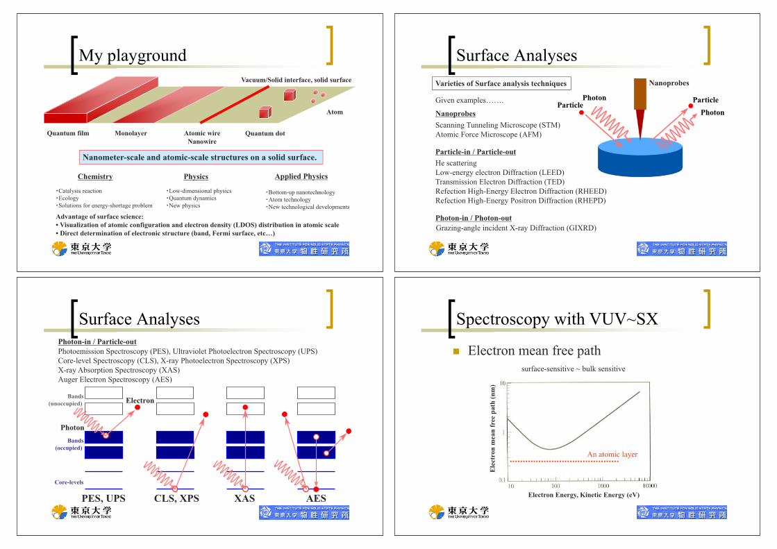
Quantum film Monolayer Atomic wireNanowire
Quantum dot
Atom
Vacuum/Solid interface, solid surface
Advantage of surface science: • Visualization of atomic configuration and electron density (LDOS) distribution in atomic scale• Direct determination of electronic structure (band, Fermi surface, etc…)
Nanometer-scale and atomic-scale structures on a solid surface.
Catalysis reactionEcologySolutions for energy-shortage problem
Bottom-up nanotechnologyAtom technologyNew technological developments
Low-dimensional physicsQuantum dynamicsNew physics
Chemistry Physics Applied Physics
My playground Surface Analyses
PhotonParticle
PhotonParticle
Nanoprobes
Particle-in / Particle-out
Varieties of Surface analysis techniques
Given examples…….
He scatteringLow-energy electron Diffraction (LEED)Transmission Electron Diffraction (TED)Refection High-Energy Electron Diffraction (RHEED)Refection High-Energy Positron Diffraction (RHEPD)
NanoprobesScanning Tunneling Microscope (STM)Atomic Force Microscope (AFM)
Photon-in / Photon-outGrazing-angle incident X-ray Diffraction (GIXRD)
Photon-in / Particle-outPhotoemission Spectroscopy (PES), Ultraviolet Photoelectron Spectroscopy (UPS)Core-level Spectroscopy (CLS), X-ray Photoelectron Spectroscopy (XPS)X-ray Absorption Spectroscopy (XAS)Auger Electron Spectroscopy (AES)
Electron
Photon
PES, UPS CLS, XPS XAS AES
Core-levels
Bands(occupied)
Bands(unoccupied)
Surface Analyses Spectroscopy with VUV~SX
surface-sensitive ~ bulk sensitive
� Electron mean free path
Ele
ctro
n m
ean
free
pat
h (n
m)
Electron Energy, Kinetic Energy (eV)
An atomic layer
Page 3
Probing electronic states� Photoelectron spectroscopy
Electron
Photon
PES, UPS CLS, XPS
Core-levels
Bands(occupied)
Bands(unoccupied)
Vacuum level
Probing electronic states
Probing electronic statesCLS, XPSESCA (Electron Spectroscopy for Chemical Analysis)
Chemical shifts
What can be probed by photoemission
Fermi level
Vacuum level
Energy shift of core-levels- Different elements- Different chemical sites (environments)
Band Dispersions of- partially occupied states (metal)- fully occupied states (semiconductor)
Page 4
� Energy range to probe - atomic structure - electronic structure- spin structure
surface sensitive ~ bulk sensitivespecification of all elementsstructure determination with high accuracyspin magnetic moment, orbital magnetic moment direct determination of spin-resolved electronic structure
Spectroscopy with VUV~SX
Semiconductor surface
Atomic structure
Silicon Si)Diamond structure
Cutting (expectation)
Dangling-bonds
Scanning Probe MicroscopeScanning Tunneling Microscope (STM)
Rohrer and Binnig (1982)
Page 5
STM Scanning Tunneling Microscope
An experimental chamber
- the Ultra High Vacuum condition
- Isolation of vibration
- Sample surface preparation
An STM image
The 7a1x1 (a1x1:3.8 ) periodicity: The Si(111)7x7 surface
Ideal surface Real surface (STM image)
G. Binnig, H. Rohrer et al., Phys. Rev. Lett. 50 (1983) 120.
It’s just an image of atomic scale protrusions measured through tunneling currents.
What are them?
Tunneling currents between unoccupied states and occupied states near Fermi level (EF).
Scanning Tunneling Microscope
Protrusions in STM could be surface atoms
Page 6
F
Dimaer-Aadatom-Stacking Fault (DAS) model
Atomic StructureK. Takayanagi et al., Surf. Sci. 164, 367 (1985).
Si(111)7x7
Core-levels
C1: Atom binding to the adatomC2: Rest atomC3: Adatom C4: Dimer atom C5: Surface impurity atom
Surface components
R. I. G. Uhrberg et al., Phys. Rev. B 58, R1730 (1998).
DAS model
AdatomRestatom
Electronic structure
Semiconductor surface
Electronic states of Si(111)7x7
restatomadatom
DAS model
Bulk Valence Band
Bulk Conduction Band
� Bonding states
# of dangling bonds in the 7x7 unit cell
AdatomRestatomCorner-
hole
Dangling-bond states
Page 7
Band mapping� Angle-resolved photoemission spectroscopy
(ARPES)
Band dispersion E,k//
ARPES measurement
�
M
K
[101]
1x1 SBZ
Energy spectra at various angles along symmetric crystal axis
Conventional measurements
P. Martensson et al., Phys. Rev. B 36, 5974 (1987).
Si(111)7x7
Dangling bonds
Rest atom state(Fully occupied)
Adatom state(Partially occupied)
- Charge transfer- Metallic surface
R. Losio et al., Phys. Rev. B 61, 10845 (2000).
DAS model
AdatomRestatom
HV-Amplifier
HV-Amplifier
HV-Amplifier
sample
tip
FeedbackElectronics
Display
XY-Ramp
Z-Control
I’V’(I’)
U’
XX
YY
Z
Lock-inAmplifier
X Y
Signal (dI/dV)
Function Generator
Reference
X,Y,ZPiezoTube V’ = V + � sin�tBias Modulation:
Current Modulation: I(V + � sin�t) = I(V) + � sin�tdIdV
Detection by phase matching
dIdV LDOS (Local Density Of States)
Scanning Tunneling Spectroscopy (STS), dI/dV
C. Bai, Scanning Tunneling Microscopy and its Application(Springer,1992)
1.0Sample Voltage (V)
dIdV
STM
R. M. Feenstra et al.,Phys. Rev. B 66, 165204 (2002)
C
dI/dV
dI/dV
A
B
G. Nicolay et al., Phys. Rev. B 62 1631 (2000).
Scanning Tunneling Spectroscopy
Page 8
Scanning Tunneling SpectroscopyDifferential Current Imaging Tunneling SpectroscopyTunneling Spectroscopy at different sire
UPS IPS
Adatom state @ - 0.35 V
Rest atom state @ - 0.8 V
Back bond state @ - 1.7 V
Si(111)7x7
R. J. Hamers et al., Phys. Rev. Lett. 56, 1972 (1986).
DAS model
AdatomRestatom
Electron Diffraction
Si(111)7x7
(Electron) Wave diffracts at a periodic structure.
15 keV
Reflection High-Energy Electron Diffraction (RHEED)
Reflection High-Energy Electron Diffraction
� RHEED pattern of Si(111)7x7 at 15 keV Si(111)7x7
Si(111)5x2-Au
Si(111)�3x�3-Ag
+ 1 ML Ag
+ 0.4 ML Au
Variations of ordered surface phases
Numerous numbers of ordered phases- Adsorbates (atom, molecule)- Coverage - Co-deposition- Substrate- Deposition temperature- Deposition rate- Deposition steps- ….
> 300 reportedfor Si substrate
S. Hasegawa et al., Prog. Surf. Sci. 60, 89 (1999).
Page 9
Si(111)�3x�3-Ag� STM image � STM simulation
Tunneling current distribution
SiAg
S. Watanabe et al., Phys. Rev. B 44, 8330 (1991).
Structure model
Si(111)�3x�3-Ag
STM protrusions do not match the atom positions.
Ag
Si
Si(111)�3x�3-Ag� Atomic Structure and CLS spectra
Si(111)�3x�3-Ag� Atomic Structure and CLS spectra
S1S2
R.I.G Uhrberg et al., Phys. Rev. B 65, 081305(R) (2002).
Page 10
Bin
ding
Ene
rgy
(eV
)
k// ( -1)
Fermi levelEF
Fermi surface
Si(111)�3x�3-Ag� Electronic Structure
- Metallic surface-state band in the bulk band gap
Si(111)�3x�3-Ag� Electronic Structure
Angle-Distribution Curves (ADC) Energy-Distribution Curves (EDC)
Si(111)�3x�3-Ag� Electronic Structure
2D-fitHV-Amplifier
HV-Amplifier
HV-Amplifier
sample
tip
FeedbackElectronics
Display
XY-Ramp
Z-Control
I’V’(I’)
U’
XX
YY
Z
Lock-inAmplifier
X Y
Signal (dI/dV)
Function Generator
Reference
X,Y,ZPiezoTube V’ = V + � sin�tBias Modulation:
Current Modulation: I(V + � sin�t) = I(V) + � sin�tdIdV
Detection by phase matching
dIdV LDOS (Local Density Of States)
Scanning Tunneling Spectroscopy (STS), dI/dV
C. Bai, Scanning Tunneling Microscopy and its Application(Springer,1992)
1.0Sample Voltage (V)
dIdV
STM
R. M. Feenstra et al.,Phys. Rev. B 66, 165204 (2002)
C
dI/dV
dI/dV
A
B
G. Nicolay et al., Phys. Rev. B 62 1631 (2000).
Scanning Tunneling Spectroscopy
Page 11
Si(111)�3x�3-Ag� Electron Standing wave
at monatomic step
I. Matsuda et al., Phys. Rev. Lett. 93, 236801 (2004).
Si(111)�3x�3-Ag� Electron Standing wave
STM(Vt: -0.7 V)
dI/dV(Vt: -0.9 V)
dI/dV(Vt: -0.7 V)
� The 2-D Free electron metallic band
Si(111)�3x�3-Ag
Electronic structure
Metal surface
Page 12
Cu(111)
L gap
F. Reinert et al., Phys. Rev. B 63, 115415 (2001).
Surface state in L point gap
G. Nicolay et al., Phys. Rev. B 65, 033407 (2001).
Ag(111)
F. Reinert et al., Phys. Rev. B 63, 115415 (2001).
Au(111)
J. Henk et al., Phys. Rev. B 68, 165416 (2003)
Appearance of the two surface-state bands
Surface Rashba effect
))((4 22 LspV
cmH
eSOC
����������
Time reversal symmetry: E(k,�)=E(-k,�)
Space inversion symmetry: E(k,�)=E(-k,�)
Pauli matrix
Electric field(0,0,Ez)
Spin-Orbit CouplingHamiltonian
E. I. Rashba, Sov. Phys. Solid State 2, 1109(1960)
Spin-split bands
Breakdown at a surface
Kramers degeneracy : E(k,�)=E(k,�)
Page 13
Spin-orbit splitting
Au(111)
J. Henk et al., Phys. Rev. B 68, 165416 (2003)
Spin-slit surface-state band
Spin-resolved photoemission spectroscopy
Fermi surface mapping with spin-resolved photoemission spectroscopyH. Moritz et al., J. Elec. Spec. Rel. Phenom. 124, 263 (2002).
COmplete PHotoEmission Experiment (COPHEE)
kx,ky,kz,x,y,z are determined with synchrotron radiation
Mott detector
M. Hoesch et al., Phys. Rev. B 69, 241401(R) (2004)
Au(111)Surface Rashba effect
Page 14
Electronic structure
Metal films
Quantum Size effect, Quantum Confinement Effect
Energetically quantized electronic statesQuantum Well States (QWS)
Fermi sphere
boundary condition� + 2 kz d + ��� ���n���
momentum space
Fermi ring(cylinder)
discrete
Free electron model
A problem of particles (electrons) in a box
Hypersurface
3-D Crystalfcc Surface BZ
3-D Brillouin Zone
QWS
Ag crystal
Fermisurface boundary condition
� + 2 kenv d + ��� ���n���
Quantum Confinement EffectQuantization of a bulk band
z
n=1
n=2
n=3
Uktrathin Ag(111) film (quantum film)
weight: spectral intensity
(15 ML-Ag(111) free-standing slab)
Fermi surface of Ag(111) slab calculation
Summation of the wave functions of + kz and -kz
6-foldsymmetry
Page 15
kx
k y( -1)
(-1
)
Kinetic Energy
In addition to band features expected, new features, kinks, hexagons at ���are observed.
Epitaxial 15ML-Ag(111) film on Si(111)
Ultrathin film (2-D growth)
Our interests
semiconductor
metal
Engineering Fermi surface topologyElectronic topological transitionby an interface monatomic layer
Surface topmost layer
Interface monatomic layer
QWS
Semiconductor Surface Science
Thickness : Semiconductorde Broglie wave, ~ 100 nmMetalFermi wavelength, ~ 1nm
Large ratio of a surface (interface) monatomic layer to film atomic layers: > 1 / 10
Quantum Size effect, Quantum Confinement Effect
STM image
Choice in Semiconductor Surface Science
Photoemission Fermi surface
aint = 1.3 nm
A periodic array of atomic wires:
Si(111)4x1-In
kF ~ 0.5 -1
Si(111)7x7
Si(111)4x1In
In deposition(HT:~600K)
Si(111)4x’2’-In
Si(111)8x2-In
Ag deposition(LT:~120-150K)
Ag thin filmon 7x7
EpitaxialAg thin filmon 7x7
EpitaxialAg thin filmon 4x1-In
Anneal (RT) ARPES
Ag thin filmon 4x1(4x’2’)-In
Substrate: vicinal Si(111) (1.8 -off)
Exchange of interface layer between film and substrate
2-D
1-D
Experiments
Page 16
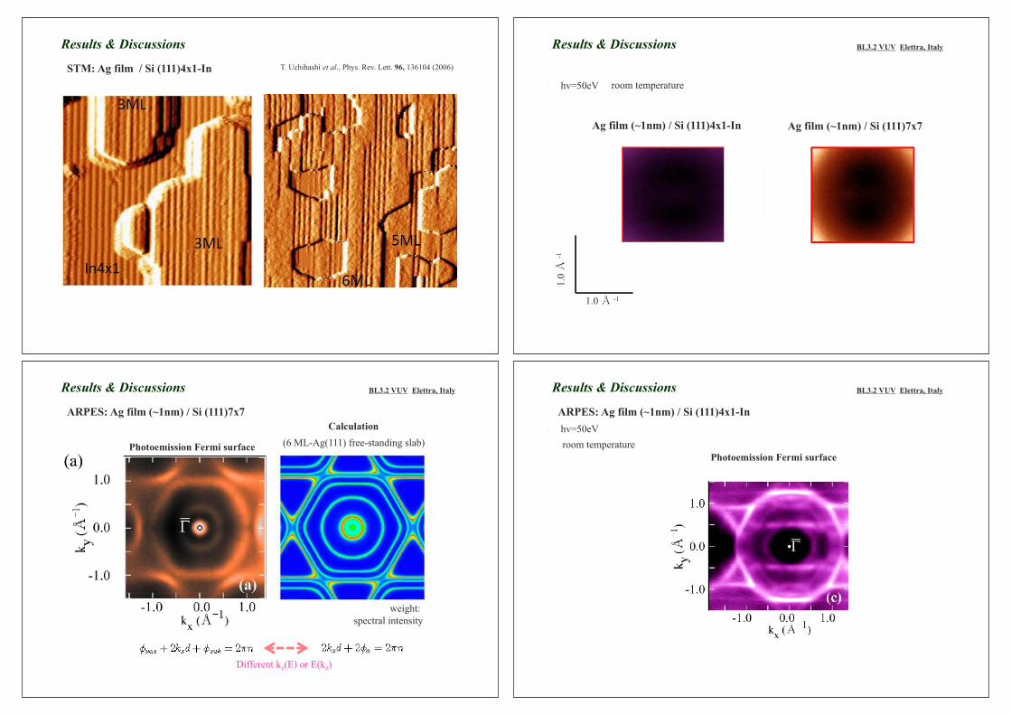
Results & Discussions
STM: Ag film / Si (111)4x1-In T. Uchihashi et al., Phys. Rev. Lett. 96, 136104 (2006)
Results & Discussions
1.0 -1
1.0
-1
BL3.2 VUV Elettra, Italy
Ag film (~1nm) / Si (111)7x7Ag film (~1nm) / Si (111)4x1-In
hv=50eV room temperature
ARPES: Ag film (~1nm) / Si (111)7x7
Results & Discussions BL3.2 VUV Elettra, Italy
weight: spectral intensity
(6 ML-Ag(111) free-standing slab)Calculation
Photoemission Fermi surface
Different kz(E) or E(kz)
Photoemission Fermi surface
ARPES: Ag film (~1nm) / Si (111)4x1-In
Results & Discussions BL3.2 VUV Elettra, Italy
hv=50eVroom temperature
Page 17
Solid Surface
Playgrounds for low-dimensional physics
Surface electronic structures
Schroedinger electron
Dirac-Wely electron
Surface Rashba effect
Quantum Spin Hall Phase
Spin-orbit interaction
Dirac equation:
Surface electronic structures
Kane,Mele, PRL(2005), Bernevig, Zhang, PRL (2005)
• bulk = gapped (insulator)• gapless edge states -- carry spin current, topologically protected
robust against nonmagnetic impurities • spin analogue of the quantum Hall effect “new state of matter”• no field required
2D 3D
Spin current(Kramers pair of gapless edge states)
2D-edge statessurface states1D-edge states
Quantum spin Hall phase (topological insulator)
Page 18
Typical surface states within the bulk band gap
(ex. Si, Ge)
- Schockley states- Tamm states
- spin-degenerateZ2 invariants: zero
Surface states of (semi)metal crystals
with strong spin-orbit interaction(ex. Bi, Au)
-Rashba effect
- spin-splitZ2 invariants: zero
Edge-states of topological insulators
(ex. Bi0.9Sb0.1)
-Odd number of Fermi level crossings
- spin-splitZ2 invariants: nonzero
Surface electronic structures No inversion symmetry
� �� �)(Pf
)(det
i
ii w
w��
�� ��
�N
mimi
12��1�i�
Z2 topological numbers: products of the parity eigenvalues
time-reversal invariant,satisfying ��i=�i+G
1/8�of�the�3D�Brillouin�Zone�(BZ)
With inversion symmetry Parity:
expressed as the productover all eight points
given by products of four � s for which �i reside in the same plane
time-reversal invariant momenta, �+
+++
+ ++ +
+++
(001) 2D-BZ with Fermi arcs of surface states enclosing the specific � points
Z2 topology in band structure
If the two k-points have opposite signs, the Fermi surface crosses between the two points.
(001)
nkmkmn uukw ,,)( � �
�Parity eigenvalue+1: symmetric-1: asymmetric Time-reversal
operator
Topological band theory
Bi0.9Sb0.1
Odd number (five) of Fermi points between � and M.
Experiment
Theory(111) 2D-BZ
+�
�
ARPES
Existence of Fermi crossing of a spin-nondegenerate band between � and M.
Agreement
theory: Fu et al., Phys. Rev. Lett. (’07)exp.: Hsieh et al., Nature (’08)
The Bi1-xSbx case
ARPES
Bi0.9Sb0.1
theory: Fu et al., Phys. Rev. Lett. (’07)exp.: Hsieh et al., Nature (’08)
Spin-polarizedband structure?
Spin- and angle(momentum)-resolved photoemission spectroscopy
How do we determine their spin coordinates?
How do we determine momentum of electrons?Electron spectrometers from VG, Scienta, Omicron, Specs….
Spin detector , Spin polarimeter
MotivationElaborateband structure?
Page 19
Spin-detector (Mott detector)
by A. Kakizaki et al.25 kV-Compact Mott detector
- 25 keV electrons- spin-orbit interaction- Au target
T.Hirahara et al., Phys. Rev. B 76,153305 (2007).
Spin-resolved band mapping of Bi crystal film with a 25 kV-Compact Mott detector
Rashba effect of the surface state
Spin-detector (Mott detector)
H. Moritz et al., J. Elec. Spec. Rel. Phenom. 124, 263 (2002).
COmplete PHotoEmission Experiment (COPHEE)
Mott detector
Spin-resolved band mapping of Bi1-xSbx crystal with a Compact Mott detector
Hsieh et al., Science 323, 919 (2009).
Bi0.9Sb0.1
�E= 100~200meV
Low spin efficiency
Spin-detector (Mott detector)Very Low- Energy Electron Diffraction (VLEED) detector
O/Fe(001)
Fe(001)
Spin-detector (VLEED detector)
T. Okuda, Y. Takeichi, Yuuki Maeda, A. Harasawa, I. Matsuda, T. Kinoshita, and A. Kakizaki, Rev. Sci. Instrum. 79, 123117 (2008).
by T. Okuda et al.
- 6 eV electrons- exchange interaction- Fe, O/Fe target
Page 20
SPECS-PHOIBOS150+VLEED detector
High-efficient spin detection (100 times better than the Mott detector)
A combination with high-resolution analyzer
���E< 30 meV
Spin-detector (VLEED detector)
ARPES
Odd number (five) of Fermi points between � and M.
Bi0.9Sb0.1
theory: Fu et al., Phys. Rev. Lett. (’07)exp.: Hsieh et al., Nature (’08)
Spin-polarized band structure?
high-resolution spin-resolved photoemission spectroscopy
Motivation
high-resolution spin-resolved photoemission spectroscopy
T~130 KSeff = 0.32 0.04,determined by the polarizationof secondary electrons from Fe(001).
�E =50 meV, ��= 1
He I�(21.2 eV)
x=0.12Measurement condition
Results and Discussion
Bi1-xSbx
x=0.12,0.13
Results and Discussion
Page 21
Edge-states of topological insulators
(ex. Bi~0.9Sb~0.1)
-Odd number of Fermi level crossings
- spin-split
- Z2 invariants: nonzero
Spin-resolved band plots on spin-integrated grayscale band diagram
Results and Discussion
D. Hsieh et al., Nature 460 1101 (2009). Y. Xia et al., Nature Phys. 5 398 (2009).
Bi2Se3 Bi2Te3
H.Zhang et al., Nature Phys. 5 438 (2009).
Well-defined stoichiometrySingle-band (One Kramers pair)Wide bulk band gap (300 meV, 3600 K)
The second generation samples
Surface Science is everywhere. Global to Atomic scale.
For solid/vacuum interface (solid surface), we have advantages of
Solid surfaces are important playgrounds for studying low-dimensional physics.
Photoemission spectroscopies with synchrotron radiation are the important experimental tools.
Summary
• Visualization of atomic configuration and electron density (LDOS) distribution in atomic scale• Direct determination of electronic structure (band, Fermi surface, spin, etc…)
Frontier Spectroscopy experiments at SPring-8 BL07LSU: with time-resolution and at nano-space
Page 22
SPring-8 BL07LSU SpecificationHigh-brilliant soft x-rayhv: 250 eV 2 000 eVresolution: E/�E: >10,000Beam size x < 10 �m
(x < 90 nm with ZP)(x < 400 nm with K-B mirror)
Flux 1012 photons/sPolarization linear, circularSR pulse-width: ~ 40 ps
Monochromator:Slit-less variable included angle VLS-PGM
Four spectroscopy end-stations
Free-Port station
Spatial resolution: 50 nm x,yDepth profile 0.1 nm z
Ultimate resolutionMeasurement of solid, liquid, gas
Open for experimental system of users
SPring-8 BL07LSU
Time-resolved angle-resolved photoemission spectroscopywith a 2D-ARTOF spectrometer and fs-pulse lasers
ARTOF
VG CLAM2
Manipulator
The measurement system
Laser system Wavelength : 200-800 nmPulse: < 50fs, Power: nJ/pulse (1kHz - 80 MHz)
2.5 mJ/pulse (1-2 KHz)
Page 23
� �� �
E-scan
�
�
Si(111) bulk valence band, hv=250 eV
Pump(laser)-Probe(synchrotron radiation) time-resolved photoemission experiments on relaxation after the surface photovoltage effect of Si(111)7x7
Element and chemical analysis in nano-region
Page 24
Thank you for your kind attentions.


![SOME PANCHAETOTHRIPINAE FROM NEPAL, MALAYSIA AND … · 2019-04-25 · SOME PANCHAETOTHRIPINAE FROM NEPAL, MALAYSIA AND THE PHILIPPINES [THYSANOPTERA: TEREBRANTIA: THRIPIDAE] By IWAo](https://static.documents.pub/doc/80x56/5f0f6e777e708231d44420ea/some-panchaetothripinae-from-nepal-malaysia-and-2019-04-25-some-panchaetothripinae.jpg)


