Photoinduced Electron Transfer and Enhancement of Photoconductivity in Silicon Nanoparticles/Perylene Diimide Composites in a Polymer Matrix Nan Liu, †,‡ Min-Min Shi, †,‡ Xiao-Wei Pan, †,‡ Wei-Ming Qiu, † Jian-Hui Zhu, †,‡ Hai-Ping He, ‡ Hong-Zheng Chen,* ,†,‡ and Mang Wang* ,†,‡ Department of Polymer Science and Engineering, Key Laboratory of Macromolecule Synthesis and Functionalization (Zhejiang UniVersity), Ministry of Education, Zhejiang UniVersity, Hangzhou 310027, P. R. China and State Key Laboratory of Silicon Material, Hangzhou 310027, P. R. China ReceiVed: March 13, 2008; ReVised Manuscript ReceiVed: July 31, 2008 An inorganic-organic hybrid composite was prepared from a soluble N-dodecyl-N′-phenyl-3,4,9,10- perylenetetracarboxylic diimide (DOPP) and silicon nanoparticles (NPs). The silicon NPs were synthesized by a solution-phase method. Remarkable photoluminescence (PL) quenching was observed in the composite dispersed in a polymethyl methacrylate matrix. On the basis of the analysis of the PL quenching mechanism, it was demonstrated that a photoinduced electron transfer from silicon NPs to DOPP could occur in the composite. The photoconductivity of the composite was studied, and the photosensitivity enhancement of the composite was realized due to the photoinduced electron transfer between silicon NPs and DOPP. Introduction Organic-inorganic nanoparticle composites have attracted great attention due to their potential applications in optoelec- tronic devices. 1-5 Many inorganic nanoparticles (NPs) were employed in this field, such as CdS, 1,2 CdSe, 3 CdTe, 4 and so on. However, due to the toxicity of Cd, compounds containing Cd element are unsuitable for consumer products. So, it is necessary to use other nontoxic materials to replace them. Silicon is a nontoxic material and is regarded as the basic material of the modern microelectronic industry because of its low cost and superior chemical and electrical properties. 5 Many preparation methods for silicon NPs have been developed, such as silicon wafer anodization, 6 laser ablation, 7 and nonthermal plasma synthesis. 8 The solution-phase synthesis of silicon NPs was recently reported by Kauzlarich and co-workers. 9,10 Com- pared with others, this method can provide a better means to control the surface passivation/termination of the NPs, which is crucial to the application of silicon NPs. On the other hand, perylene diimide derivatives, as typical organic electron acceptor semiconductors with high electron mobility, have been used to prepare photovoltaic and photo- conductive devices. 11,12 However, due to their poor solubility, the devices based on them were prepared mostly by vapor deposition method, which is costly and inconvenient. Here, we introduced a simple method to fabricate inorganic- organic hybrid composites from N-dodecyl-N′-phenyl-3,4,9,10- perylenetetracarboxylic diimide (DOPP) and silicon NPs. On the basis of the analysis of the photoluminescence (PL) quenching mechanism, we tried to demonstrate that a photoin- duced electron transfer from silicon NPs to DOPP could occur in the composites, which could remarkably improve the photoconductivity of the composites. Experimental Section Silicon NPs were synthesized via the reduction of silicon tetrachloride (SiCl 4 ) with sodium naphthalide according to the published method, 9 and all reactions were carried out in a Schlenk line. A 0.18 g portion of sodium and 0.74 g of naphthalene were stirred in 20 mL of 1,2-dimethoxyethane (glyme) for 24 h to produce sodium naphthalide, which was rapidly added via a syringe into 0.26 g of SiCl 4 in 60 mL of glyme. The reaction lasted for 40 min before 1.25 mL of 1-octanol was added. Then, the reaction mixture was stirred for 12 h, giving an orange solution with white precipitates. The solvent and the unreacted naphthalene were removed under reduced pressure in a water bath. The resulted orange solid was then washed three times with chloroform or hexane, giving an orange solid of silicon NPs. Silicon NPs synthesized in this way were terminated with n-octanol. N-dodecyl-N′-phenyl-3,4,9,10-perylenetetracarboxylic diim- ide (a) was synthesized and purified according to our previously published procedures. 13 The prepared compound a (0.24 g) was then added together with aniline (l ml) and zinc acetate (0.2 g) in 15 mL of quinoline. The reaction lasted for 12 h. Then, the reaction mixture was washed several times with ethanol, KOH solution, and acetone, followed by a drying process at 100 °C in a vacuum oven. The resulted solid was purified by temper- ature gradient sublimation, giving 0.19 g of red powders with a yield of 67.7%. Anal. Calcd. for DOPP (C 42 H 38 N 2 O 4 ) (%): C, 79.47; N, 4.41; H, 6.03. Found: C, 79.41; N, 4.64; H, 5.35. FTIR (KBr, pellet): υ ) 1698, 1658 cm -1 (CdO). A certain amount of polymethyl methacrylate (PMMA), silicon NPs, and DOPP were dissolved in chloroform to give a mixed solution. The concentration of DOPP was defined as follows: C ) M 2 M 1 + M 2 (1) where C is the concentration of DOPP, and M 1 and M 2 indicate the mass of silicon NPs and DOPP, respectively. The concentra- tion of silicon NPs was kept constant and that of DOPP varied * Corresponding author e-mail: (H.Z.C.) [email protected], (M.W.) [email protected]. † Zhejiang University. ‡ State Key Laboratory of Silicon Material. J. Phys. Chem. C 2008, 112, 15865–15869 15865 10.1021/jp802385g CCC: $40.75 2008 American Chemical Society Published on Web 09/09/2008
Transcript
Photoinduced Electron Transfer and Enhancement of Photoconductivity in SiliconNanoparticles/Perylene Diimide Composites in a Polymer Matrix
Nan Liu,†,‡ Min-Min Shi,†,‡ Xiao-Wei Pan,†,‡ Wei-Ming Qiu,† Jian-Hui Zhu,†,‡ Hai-Ping He,‡Hong-Zheng Chen,*,†,‡ and Mang Wang*,†,‡
Department of Polymer Science and Engineering, Key Laboratory of Macromolecule Synthesis andFunctionalization (Zhejiang UniVersity), Ministry of Education, Zhejiang UniVersity, Hangzhou 310027,P. R. China and State Key Laboratory of Silicon Material, Hangzhou 310027, P. R. China
ReceiVed: March 13, 2008; ReVised Manuscript ReceiVed: July 31, 2008
An inorganic-organic hybrid composite was prepared from a soluble N-dodecyl-N′-phenyl-3,4,9,10-perylenetetracarboxylic diimide (DOPP) and silicon nanoparticles (NPs). The silicon NPs were synthesizedby a solution-phase method. Remarkable photoluminescence (PL) quenching was observed in the compositedispersed in a polymethyl methacrylate matrix. On the basis of the analysis of the PL quenching mechanism,it was demonstrated that a photoinduced electron transfer from silicon NPs to DOPP could occur in thecomposite. The photoconductivity of the composite was studied, and the photosensitivity enhancement of thecomposite was realized due to the photoinduced electron transfer between silicon NPs and DOPP.
Introduction
Organic-inorganic nanoparticle composites have attractedgreat attention due to their potential applications in optoelec-tronic devices.1-5 Many inorganic nanoparticles (NPs) wereemployed in this field, such as CdS,1,2 CdSe,3 CdTe,4 and soon. However, due to the toxicity of Cd, compounds containingCd element are unsuitable for consumer products. So, it isnecessary to use other nontoxic materials to replace them.Silicon is a nontoxic material and is regarded as the basicmaterial of the modern microelectronic industry because of itslow cost and superior chemical and electrical properties.5 Manypreparation methods for silicon NPs have been developed, suchas silicon wafer anodization,6 laser ablation,7 and nonthermalplasma synthesis.8 The solution-phase synthesis of silicon NPswas recently reported by Kauzlarich and co-workers.9,10 Com-pared with others, this method can provide a better means tocontrol the surface passivation/termination of the NPs, whichis crucial to the application of silicon NPs.
On the other hand, perylene diimide derivatives, as typicalorganic electron acceptor semiconductors with high electronmobility, have been used to prepare photovoltaic and photo-conductive devices.11,12 However, due to their poor solubility,the devices based on them were prepared mostly by vapordeposition method, which is costly and inconvenient.
Here, we introduced a simple method to fabricate inorganic-organic hybrid composites from N-dodecyl-N′-phenyl-3,4,9,10-perylenetetracarboxylic diimide (DOPP) and silicon NPs. Onthe basis of the analysis of the photoluminescence (PL)quenching mechanism, we tried to demonstrate that a photoin-duced electron transfer from silicon NPs to DOPP could occurin the composites, which could remarkably improve thephotoconductivity of the composites.
Experimental Section
Silicon NPs were synthesized via the reduction of silicontetrachloride (SiCl4) with sodium naphthalide according to thepublished method,9 and all reactions were carried out in aSchlenk line. A 0.18 g portion of sodium and 0.74 g ofnaphthalene were stirred in 20 mL of 1,2-dimethoxyethane(glyme) for 24 h to produce sodium naphthalide, which wasrapidly added via a syringe into 0.26 g of SiCl4 in 60 mL ofglyme. The reaction lasted for 40 min before 1.25 mL of1-octanol was added. Then, the reaction mixture was stirredfor 12 h, giving an orange solution with white precipitates. Thesolvent and the unreacted naphthalene were removed underreduced pressure in a water bath. The resulted orange solid wasthen washed three times with chloroform or hexane, giving anorange solid of silicon NPs. Silicon NPs synthesized in this waywere terminated with n-octanol.
N-dodecyl-N′-phenyl-3,4,9,10-perylenetetracarboxylic diim-ide (a) was synthesized and purified according to our previouslypublished procedures.13 The prepared compound a (0.24 g) wasthen added together with aniline (l ml) and zinc acetate (0.2 g)in 15 mL of quinoline. The reaction lasted for 12 h. Then, thereaction mixture was washed several times with ethanol, KOHsolution, and acetone, followed by a drying process at 100 °Cin a vacuum oven. The resulted solid was purified by temper-ature gradient sublimation, giving 0.19 g of red powders witha yield of 67.7%. Anal. Calcd. for DOPP (C42H38N2O4) (%):C, 79.47; N, 4.41; H, 6.03. Found: C, 79.41; N, 4.64; H, 5.35.FTIR (KBr, pellet): υ ) 1698, 1658 cm-1 (CdO).
A certain amount of polymethyl methacrylate (PMMA),silicon NPs, and DOPP were dissolved in chloroform to give amixed solution. The concentration of DOPP was defined asfollows:
C)M2
M1 +M2(1)
where C is the concentration of DOPP, and M1 and M2 indicatethe mass of silicon NPs and DOPP, respectively. The concentra-tion of silicon NPs was kept constant and that of DOPP varied
† Zhejiang University.‡ State Key Laboratory of Silicon Material.
J. Phys. Chem. C 2008, 112, 15865–15869 15865
10.1021/jp802385g CCC: $40.75 2008 American Chemical SocietyPublished on Web 09/09/2008
with 0, 2, 5, 10, and 15%. The mixed solutions were then spin-coated onto glass substrates and dried at 110 in a vacuum ovenfor 3 h, giving the silicon NPs/DOPP composites dispersed inPMMA matrix identical thicknesses of about 6 µm.
Transmission electron microscope (TEM), atomic forcemicroscope (AFM), and scanning electron microscope (SEM)images were observed on a JEM 200CX TEM, a SkeioSPI3800N AFM, and a JSM-35CF SEM, respectively. X-raydiffraction (XRD) patterns were obtained on a Pigaku D/Max-38. Fourier transform infrared (FTIR) spectra were obtained ona Vector 22 Fourier transform infrared spectroscope. Elementalanalyses were determined on a Perkin-Elmer 240C elementalanalyzer. PL spectra were taken on a HITACHI 4500 fluores-cence spectrophotometer. UV-vis absorption was recorded ona Cary Bio100 spectrophotometer. The cyclic voltammogram(CV) was taken by a CHI660 electrochemistry workstation.Time-resolved PL decays were measured on a Laserstrobefluorescence lifetime spectrometer.
Photoconductivity of silicon NPs/DOPP composites wasstudied in dual-layer photoreceptors on a GDT-II model
photoconductivity measuring device. The typical structure ofthe photoreceptors and the principle of the photoconductivitymeasuring device were depicted elsewhere.14 Photosensitivity(S) is defined as the reciprocal of half-decaying exposure energy(E1/2), and E1/2 is calculated by the product of half-decayingtime (t1/2) and the intensity of exposure light (I), that is, E1/2 )It1/2. The smaller the value of E1/2, the higher the photosensitivityof the photoreceptor. The photoreceptor was made by coatingthe interface layer (IFL), the charge generation layer (CGL),and the charge transport layer (CTL), in that order, on analuminum substrate. The IFL, CGL, and CTL were formed withPMMA (∼1 µm thickness), silicon NPs/DOPP compositesdispersed in PMMA matrix (∼6 µm thickness), and 50 wt %N,N′-diethyl-4-aminobenzaldehyde-1-phenyl-1′-(R-naphthyl)-hy-drazone in a polycarbonate matrix (∼25 µm), respectively.
Results and Discussion
The FTIR spectrum of the final product (see SupportingInformation Figure S1) indicated the presence of octanoxidegroups on the surface of the silicon NPs. The bands corre-sponding to alkyl C-H stretching at ∼3000 cm-1 and Si-ORstretching at ∼1080 cm-1 were observed. The silicon NPs werealso soluble in chloroform and hexane, making wet processingpossible.
TEM image of silicon NPs is shown in Figure 1a. The sizeis in the range of 8∼25 nm. Figure 1b is the SEM image ofsilicon NPs dispersed in PMMA matrix. It suggests a highdegree of homogeneity for the film, and no obvious aggregationof silicon NPs can be seen, which is favored for the fabricationof photoreceptors. As seen from its XRD pattern (see SupportingInformation Figure S2), the peaks are fully consistent with thecrystalline silicon.9
Figure 2 presents UV-vis absorption and PL spectra ofsilicon NPs and DOPP. According to the absorption data, theindirect band gap of silicon NPs is yielded as 1.82 eV by thefollowing formula,15
Rh)C(hν-Eg)2 (2)
where R is the absorption coefficient, hν is the photon energy,C is a constant, and Eg is the band gap energy. The PL peakfor silicon NPs is observed at ∼490 nm (2.53 eV) with a 410nm excitation. The absorption peaks for DOPP can be observedat ∼457, ∼490, and ∼525 nm, and its band gap is estimatedfrom its absorption spectrum as 2.36 eV. The PL peaks of DOPPcan also be observed at ∼540 and ∼570 nm.
Figure 1. (a) TEM image of silicon NPs. (b) SEM image of siliconNPs dispersed in PMMA matrix.
Figure 2. UV-vis absorption and PL spectra of DOPP (dash line)and silicon NPs (solid line) in PMMA matrix. The excitation wavelengthis 410 nm for both of them.
Figure 3. PL spectra of silicon NPs/DOPP composites dispersed inPMMA matrix with 0 (a), 2 (b), 5 (c), 10 (d), and 15% (e) DOPP. Theexcitation wavelength is 410 nm.
15866 J. Phys. Chem. C, Vol. 112, No. 40, 2008 Liu et al.
PL spectra of the composites with different DOPP concentra-tion are depicted in Figure 3. The spectra mainly show thecharacteristic PL features of silicon NPs due to the muchstronger PL intensity of silicon NPs than that of DOPP in thecomposites. Besides, a weak band centered at ∼570 nm canalso be observed that is attributed to DOPP emission. The PLof silicon NPs/DOPP composites is gradually quenched withincreasing concentration of DOPP in the composites. Consider-ing the large overlap of the PL of silicon NPs and the absorptionof DOPP shown in Figure 2, we deduce that a Forster resonanceenergy transfer (FRET) from silicon NPs (donor) to DOPP(acceptor) might take place. The energy transfer rate is decidedby eq 3,16
kET ) k0(R0
R )6
(3)
where kET is the energy transfer rate, k0 is radiative decay rateof the donor, R is the separation distance between the donorand the acceptor, and R0 is Forster critical distance correspondingto a rate of FRET equivalent to the rate of radiative decay, whichis given as follows,
R06 )
9000(ln 10)k2�d
128π6NAVn4 ∫ fD(ν)εA(ν)
ν 4dν (4)
where n is the film’s refractive index, N indicates Avogadronumber, Φd is the donor emission quantum efficiency, k2 is anorientation factor for which random relative orientation of thedonor and acceptor dipoles is 2/3, νj is the wavenumber, and∫(fD(νj)εA(νj)/ν 4) dνj represents the overlap integral of the
normalized donor emission spectrum (fD(νj)) and the acceptorabsorption extinction coefficient spectrum (εA(νj)). Thus, aForster critical distance of about 31 Å is calculated from eq 4,which suggests a relatively moderate energy transfer efficiency.In the composite with 10% DOPP, for instance, the averagedonor-acceptor separation distance is estimated to be 38 Å fromhard-sphere consideration of DOPP distribution, the decay rateratio (kET/k0) corresponds to 0.29, which accounts for 22.4% ofthe total photogenerated excitons undergoing energy transfer.On the other hand, a 78% decrease of the PL intensity of siliconNPs in the composite is obtained from Figure 3. The low energytransfer efficiency and large PL intensity decrease stronglysuggest a different mechanism, which results in the PL quench-ing of silicon NPs in the composites.
Three processes can lead to PL quenching,17 including energytransfer (eq 5) from the donor (D) to acceptor (A), catalyticdeactivation (eq 6) of L* (L indicates the luminophore) withoutexcitation of the quencher (Q), and electron transfer (eq 7) fromthe donor (D) to acceptor (A).
D* +AfD+A* (5)
L* +QfL+Q+∆ (6)
D* +AfD++A- (7)
Herein we use the simplified Rehem-Weller relationship todecide whether process 7 takes place,18 which is given by eq 8,
∆GPET ) e(ED⁄D+ -EA-⁄A)-E00 (8)
where ∆GPET is the free energy change, and if ∆GPET < 0, thenelectron transfer can occur between the photoexcited electron
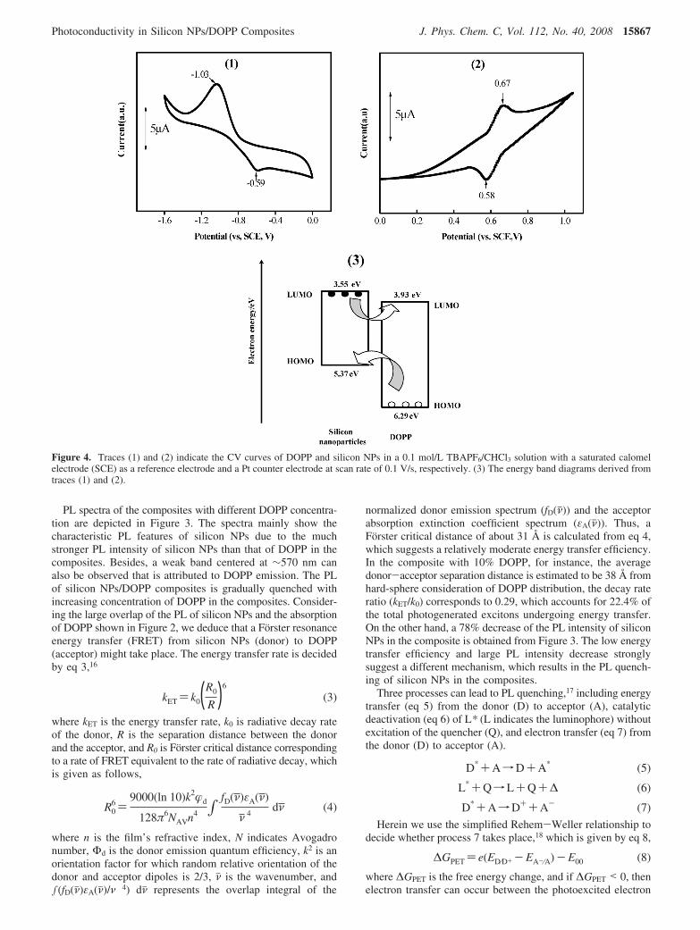
Figure 4. Traces (1) and (2) indicate the CV curves of DOPP and silicon NPs in a 0.1 mol/L TBAPF6/CHCl3 solution with a saturated calomelelectrode (SCE) as a reference electrode and a Pt counter electrode at scan rate of 0.1 V/s, respectively. (3) The energy band diagrams derived fromtraces (1) and (2).
Photoconductivity in Silicon NPs/DOPP Composites J. Phys. Chem. C, Vol. 112, No. 40, 2008 15867
donor and ground-state electron acceptor. ED/D+ and EA-/A arethe redox potentials of electron donor and acceptor, respectively.E00 is the energy of the excited-state from which electron transferoccurs.
The typical CV of silicon NPs and DOPP are shown in Figure4, traces (1) and (2), from which the ED/D+ and EA-/A wereestimated as 0.67 and -1.03 V, respectively, for the electrontransfer from silicon NPs to DOPP. E00 is estimated as theemission energy of silicon NPs (2.53 eV).18 ∆GPET is thuscalculated to be negative (-0.83 eV). Therefore, photoinducedelectron transfer from silicon NPs to DOPP may take place intheir composites.
The highest occupied molecular orbital (HOMO) of siliconNPs is estimated as 5.37 eV according to the half-wave potentialvalue obtained from Figure 4, trace (1). Thus, the lowestunoccupied molecular orbital (LUMO) of silicon NPs can beestimated as 3.55 eV. Similarly, LUMO and HOMO of DOPPare calculated as 3.93 and 6.29 eV, respectively. Figure 4, panel(3), gives the energy band diagrams of silicon NPs and DOPP.At silicon NPs/DOPP interfaces, a LUMO offset of 0.38 eVand a HOMO offset of 0.92 eV can be observed, which isfavored for the electron transfer from silicon NPs to DOPP.
Figure 5 presents the PL decays of silicon NPs/DOPPcomposites dispersed in PMMA matrix monitoring the PL forsilicon NPs. The decay curves are fitted by a biexponentialfunction:
I(t))R1e-t⁄τ1 +R2e
-t⁄τ2 (9)
where I is the PL intensity at time t, τ1 and τ2 are the lifetimesof the two components with the preexponential factors of R1
and R2. The average lifetime (τj) is defined as the time whenthe PL intensity has decayed to e-1 times its original value.19a
τ1, τ2, and the average lifetimes are listed in Table 1. As isshown, the lifetime of silicon NPs is prolonged in the siliconNPs/DOPP composites compared to that of the pure silicon NPs.This is consistent with a slower recombination of the electron-
hole pairs, which results from the separation of the photoinducedcharges at the interface.19 Considering the lifetime of siliconNPs should decrease in the mentioned energy transfer donor-acceptor system (eq 5)20 and the catalytic deactivation process(eq 6),21 it is revealed that the electron transfer predominatesthe PL quenching of silicon NPs whether or not process 6occurs.
It is also noticeable that as the concentration of DOPPincreases to be 15%, the lifetime of silicon NPs is graduallyshortened. Atomic force microscopy (AFM) images of pristineDOPP dispersed in PMMA matrix are shown in Figure 6. Itcan be seen that when the concentration of DOPP is increasedto 15%, the obvious aggregation of DOPP occurs. On the basisof this, we deduce that two reasons may be responsible for thisobservation. First, although the concentration of DOPP increases,it does not mean a larger silicon NPs/DOPP interface area. MoreDOPP molecules may not directly contact silicon NPs butaggregate with each other, which can not contribute to theelectron transfer. But energy transfer is a “long-range” transfer,and it can occur at the intermolecular separation distance e100Å. Thus, DOPP not directly contacting silicon NPs maystrengthen the energy transfer from silicon NPs to DOPP, whichdecreases the electron transfer efficiency and also the lifetimeof silicon NPs. Second, the aggregation of DOPP seems to resultin more defect sites, which can lead to the occurrence of process6, where the defect sites act as Q. Thus, the electron transferefficiency and the lifetime of silicon NPs also decrease.
The photoconductivity properties of silicon NPs/DOPPcomposites with different DOPP concentrations are shown inTable 2. It is found that the photosensitivity (S) of silicon NPs/DOPP composites increases from 19.18 to 28.49, 39.88, and77.70 × 10-3 µJ-1 mm2 with increasing content of DOPP from0 to 2, 5, and 10% in the composites, but when the DOPPconcentration is beyond 10-15%, the S value of silicon NPs/DOPP composites decreases from 77.70 to 52.85 × 10⁻³ µJ-1
mm2. In our photoconductivity measurements, a higher S valuecorresponds to a higher electron transfer efficiency. As DOPPconcentration rises, the changes of the S value indicate the
Figure 5. PL decays monitoring the PL peak of silicon NPs in thecomposites with 0 (9), 2 (•), 5 (2), 10 (0), and 15% (1) DOPPconcentration. The solid lines are the best-fit curves.
TABLE 1: PL Lifetimes at the Indicated EmissionWavelength (490 nm) for Silicon NPs in Silicon NPs/DOPPComposites Dispersed in PMMA Matrix
Figure 6. AFM images (10 × 10 µm) of the pristine DOPP filmsdispersed in PMMA matrix corresponding to (a) 2, (b) 5, (c) 10, and(d) 15% DOPP concentration. All the films were spin-coated on glasssubstrates.
15868 J. Phys. Chem. C, Vol. 112, No. 40, 2008 Liu et al.
electron transfer efficiency in the composites is improved, butwhen DOPP concentration is beyond 10-15%, the data in Table1 suggest the decrease of the electron transfer efficiency, whichis consistent with the results of PL decays.
Conclusion
An inorganic-organic hybrid composite was prepared fromDOPP and silicon NPs. The photoluminescence quenchingmechanism of the composites dispersed in PMMA matrixrevealed a photoinduced electron transfer from silicon NPs toDOPP in the composite. Thus, the photoconductivity propertyof the composites was improved.
Acknowledgment. We are grateful for the financial supportof the National Natural Science Foundation of China (GrantNos. 50433020, 50673083, and 50520150165) and of the Fundfor the Major State Basic Research Development Program(2007CB613400). The authors also would like to thank thedeveloping program of Changjiang Scholar and Innovation Teamfrom Ministry of Education of China (Grant No IRT0651).
Supporting Information Available: FTIR spectrum ofsilicon nanoparticles synthesized by solution method. XRDpattern of silicon nanoparticles. This material is available freeof charge via the Internet at http://pubs.acs.org.
References and Notes
(1) Greenham, N. G.; Peng, X. A.; Alivisatos, P. Phys. ReV. B 1996,54, 17628.
(2) Chen, F.; Zhou, R.; Yang, L.; Liu, N.; Wang, M.; Chen, H. Z. J.Phys. Chem. C 2008, 112, 1001.
(3) Wang, S. H.; Yang, S. H.; Yang, C. L.; Li, Z. Q.; Wang, J. N.; Ge,W. K. J. Phys. Chem. B 2004, 104, 11853.
(4) Kumar, S.; Nann, T. J. Mater. ReV. 2004, 19, 1990.(5) (a) Liu, N.; Chen, H. Z.; Chen, F.; Wang, M. Chem. Phys. Lett.
2008, 451, 70. (b) Liu, N.; Chen, H. Z.; Wang, M. Thin Solid Films 2008,516, 4272.
(6) Canham, L. T. Appl. Phys. Lett. 1990, 57, 1146.(7) Li, X.; He, Y. S.; Talukdar, S.; Swihart, M. T. Phase Transitions
2004, 77, 131.(8) Mangolini, L. T.; Kortshagen, U. Nano. Lett. 2005, 5, 655.(9) Baldwin, R. K.; Pettigrew, K. A.; Ratai, E.; Augustine, M. P.;
Kauzlarich, S. M. Chem. Commun. 2002, 1822.(10) Zou, J.; Baldwin, R. K.; Pettigrew, K. A.; Kauzlarich, S. M. Nano.
Lett. 2004, 4, 1181.(11) Mo, X.; Chen, H. Z.; Wang, Y.; Shi, M. M.; Wang, M. J. Phys.
Chem. B 2005, 109, 7659.(12) Chen, H. Z.; Shi, M. M.; Aernouts, T.; Wang, M.; Borghs, G.;
Heremans, P. Sol. Energy Mater. Sol. Cells 2005, 87, 521.(13) Yang, X. G.; Sun, J. Z.; Wang, M.; Chen, H. Z. Chin. Chem. Lett.
2003, 14, 1105.(14) Cao, L.; Chen, H. Z.; Wang, M.; Sun, J. Z. J. Phys. Chem. B 2002,
106, 8971.(15) Wilcoxon, J. P.; Samara, G. A.; Provencio, P. N. Phys. ReV. B 1999,
60, 2704.(16) Forster, T. Discuss. Faraday Soc. 1959, 27, 7.(17) Demas, J. N.; DeGraff, B. A.; Xu, W. Anal. Chem. 1995, 67, 1377.(18) (a) Wang, Y. H.; Zhang, H. M.; Liu, L.; Liang, Z. X.; Guo, Q. X.;
Tung, C. H.; Inoue, Y.; Liu, Y. C. J. Org. Chem. 2002, 67, 2429. (b) Hu,H. Y.; Zhu, M. Z.; Zhang, Z. P.; Wen, G. T.; Guo, Q. X. Chin. Chem. Lett.2006, 17, 333.
(19) (a) Cheng, J.; Wang, S.; Li, X. Y.; Yan, Y. J.; Yang, S.; Yang,C. L.; Wang, J. N.; Ge, W. K. Chem. Phys. Lett. 2001, 333, 375. (b) Yang,C. L.; Wang, J. N.; Ge, W. K.; Wang, S.; Cheng, J.; Li, X. Y.; Yang, S.Appl. Phys. Lett. 2001, 78, 760. (c) Gonzalez, J.; Virgili, T.; Lanzani, G.Phys. ReV. B 2005, 71, 014211.
(20) (a) Kagan, C. R.; Murray, C. B.; Nirmal, M.; Bawendi, M. G. Phys.ReV. Lett. 1996, 76, 1517. (b) Anni, M.; Manna, L.; Cingolani, R.; Valerini,D.; Creti, A.; Lomascolo, M. Appl. Phys. Lett. 2004, 85, 4169.
(21) Frolov, S. V.; Lane, P. A.; Ozaki, M.; Yoshino, K.; Vardeny, Z. V.Chem. Phys. Lett. 1998, 286, 21.
JP802385G
TABLE 2: Photoconductivity Properties of Silicon NPs/DOPP Composites Dispersed in PMMA Matrixa
a Exposed to a light with an intensity of 11 µW mm-2 from ahalogen lamp. Abbreviations: V0, initial surface potential; Rd, darkdecay rate; Vr, residual surface potential; t1/2, half-discharge timeunder exposure; and S, photosensitivity.
Photoconductivity in Silicon NPs/DOPP Composites J. Phys. Chem. C, Vol. 112, No. 40, 2008 15869