Photoluminescence excitation spectroscopy at 9 Kreveals that the absorption edge of Ga.5In.5P containing relatively ordered domains (grown at 6700
C) is near 1.93 eV, representing the bandgap ofthis inhomogeneous material. Photoluminescencehas been observed at energies as much as 70 meVlower than this absorption edge energy. Alongwith our previous time-resolved photoluminescence results - which show unusually slow decaytimes - the low energy photoluminescence indicates spatially indirect recombination. Therefore,photoluminescence alone can not reliably determine the bandgap of typical "ordered" Ga.5In.5P
samples. In contrast, photoluminescence of relatively randomly-ordered ("normal") Ga.5In.5P
(grown at 7750 C) occurs at the same energy as theabsorption edge and exhibits a rapid decay time.These characteristics are typical of a normaldirect ill-V semiconductor.
The photoluminescence (PL) energy of Ga.sIn.sP grown lattice-matched to GaAs depends on
growth temperature and technique. Ga.sIn.sP grown at temperatures from 600 to 7000C has a
lower PL peak energy (by 50 to 135 meV) than Ga.sIn.sP grown at higher (> 7500C)
temperatures. Gomyo et al. related this behavior to different degrees of column III atomic
sublattice ordering in the crystal. 1 The ordered domains in the crystal are Ga plane, P plane, In
plane, P plane, Ga plane, ... in [111] crystal directions for growth on [100] surfaces.s These
domains exist in a randomly-ordered matrix. The size and density of the ordered domains
depend on growth parameters.vs! This low temperature-grown material is typically called
"ordered", despite its inhomogeneous composition. Ga.sIn.sP grown at higher temperatures
which exhibits high PL energies is often referred to as "normal" or "disordered", but this
material can still exhibit some limited evidence of ordering in electron diffraction
measurements.S
We previously observed the low temperature PL peak energy to vary strongly with excitation
level for "ordered" material grown from 630 to 6700C; a four order-of-magnitude increase in
excitation level shifted the peak by 15-33 meV. In contrast, "normal" Ga.sIn.sP grown at 7750 C
has a PL peak energy virtually independent of excitation level.S This behavior is typical of good
III-V materials excited at low enough levels to avoid significant bandfilling.
Our previous low temperature time-resolved photoluminescence (TRPL) studies of "normal"
Ga.sIn.sP showed a single exponential decay with a 0.7 ns time constant over a wide range of
excitation densities. This result is typical for excitonic recombination. In contrast, "ordered"
material exhibited evidence of more than one process. At high excitation the decay was 1.8 ns,
while at low excitation the dominant decay was too slow to be measured by our system, > 1 J.1s.s
Delong, et al., subsequently also reported long decay times at low energies, measuring decays
2
into the ms regime," These long decay times in material with high 300 K PL efficiencies suggest
spatially indirect recombination.s
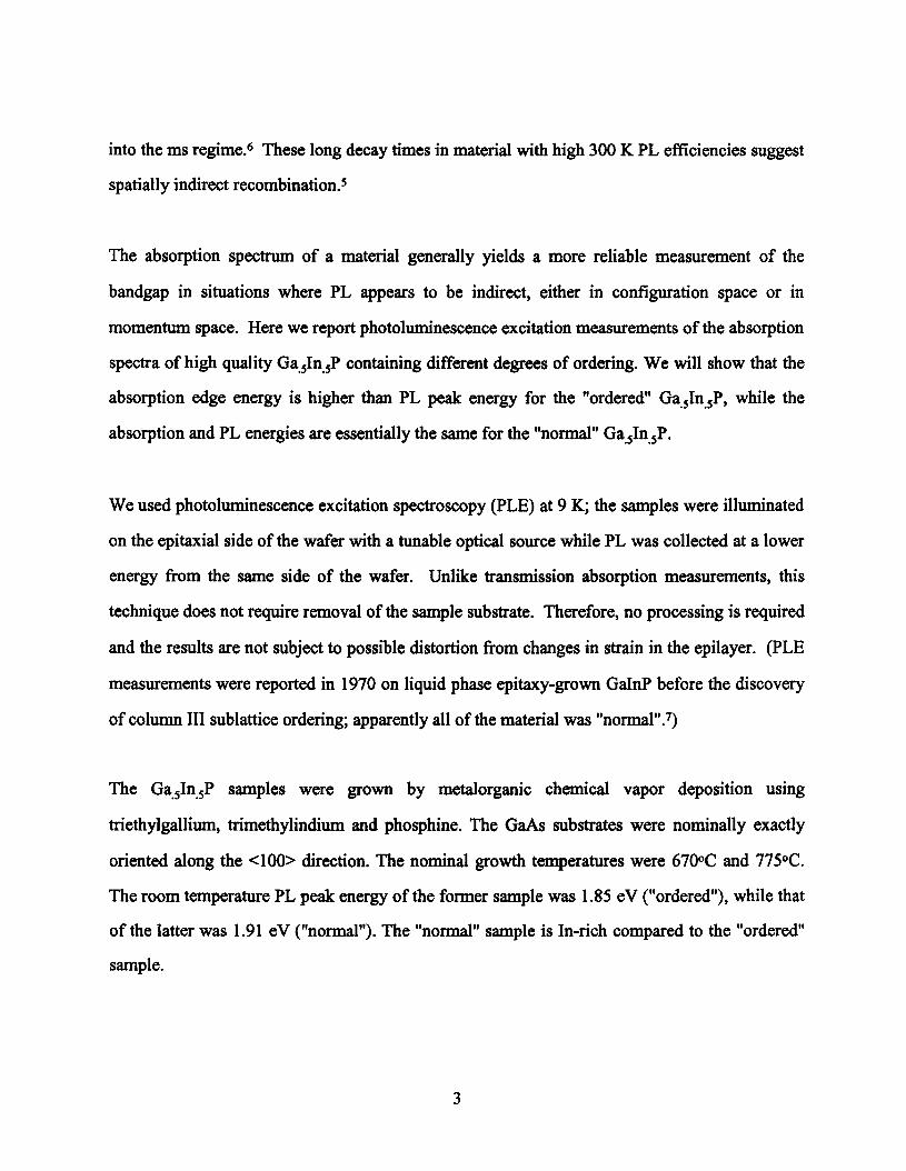
The absorption spectrum of a material generally yields a more reliable measurement of the
bandgap in situations where PL appears to be indirect, either in configuration space or in
momentum space. Here we report photoluminescence excitation measurements of the absorption
spectra of high quality Ga.sIn.sP containing different degrees of ordering. We will show that the
absorption edge energy is higher than PL peak energy for the "ordered" Ga.sIn.sP, while the
absorption and PL energies are essentially the same for the "normal" Ga.sIn.sP.
We used photoluminescence excitation spectroscopy (PLE) at 9 K; the samples were illuminated
on the epitaxial side of the wafer with a tunable optical source while PL was collected at a lower
energy from the same side of the wafer. Unlike transmission absorption measurements, this
technique does not require removal of the sample substrate. Therefore, no processing is required
and the results are not subject to possible distortion from changes in strain in the epilayer. (PLE
measurements were reported in 1970 on liquid phase epitaxy-grown GaInP before the discovery
of column III sublattice ordering; apparently all of the material was "normal",")
The Ga.sIn.sP samples were grown by metalorganic chemical vapor deposition USIng
triethylgallium, trimethylindium and phosphine. The GaAs substrates were nominally exactly
oriented along the <100> direction. The nominal growth temperatures were 6700C and 775°C.
The room temperature PL peak energy of the former sample was 1.85 eV ("ordered"), while that
of the latter was 1.91 eV ("normal"). The "normal" sample is In-rich compared to the "ordered"
sample.
3
Prior high resolution transmission electron rmcroscopy (HRTEM) measurements of our
"ordered" material showed relatively-ordered quantum "plate"-like domains within a randomly
ordered matrix. S HRTEM of the current "ordered" sample revealed that approximately half of
the material was random alloy while the other half exhibited ordering of two <111> variants.
Both laser and lamp excitation were used for PL measurements. The continuous-wave Ar ion
laser source at 488 nm was loosely focussed with a 75 em focal length lens. Neutral density
filters were used to vary the excitation power from 650 mW down to 0.005 mW. Lamp
excitation was provided by a 250 W Oriel tungsten halogen lamp focused into a 1/4 m single
spectrometer set at 499 or 573 nm (2.485 or 2.164 eV, respectively) and imaged 1:1 onto the
sample. The output of this excitation spectrometer was passed through a 455 nm long-pass filter
to remove second-order ultraviolet wavelengths. The illuminated area was approximately the
same width as the slit by more than 2 em, much larger than the spot illuminated by the laser.
The low lamp power and large illuminated area imply that the excitation density is very low in
this case. Emission from the sample was collected and passed into a 1/4 m double spectrometer
with holographic gratings. The emission spectrometer was scanned for PL measurements.
The PL emission photon energy of this "ordered" sample depended strongly on excitation power
(measured with laser excitation at one location on the sample), qualitatively similar to results
from low temperature-grown samples we observed previously. S The "normal" sample showed
no PL peak dependence on excitation power, also similar to our previous high temperature
grown material. For lamp excitation, the PL peak energy was at 1.861-1.862 eV for the
"ordered" sample and 1.973-1.974 eV for the "normal" sample.
4
For PLE measurements, the same lamp excitation source was scanned while the emission
spectrometer was held at a fixed, long wavelength. All four spectrometer slits were set to the
same width, 0.55 or 0.775 mm, corresponding to 1.0 or 1.5 nm nominal resolution, respectively.
The emission wavelength was chosen to fallon the PL spectrum obtained using lamp excitation.
Different parts of this spectral feature were chosen as emission wavelengths for PLE.
Absorption spectra for the samples are compared in Fig. 1, with PL peak energies marked by
arrows. Lamp excitation was used to obtain these PL reference energies because it approximates
the same intensity and illuminates the same area of the sample as in the PLE measurements. The
absorption of the "ordered" sample falls to 50% of its peak value near 1.93 eV, roughly 70 meV
higher than the 1.86 eV PL peak energy. In contrast, absorption of the "normal" sample falls to
50% at 1.97 eV. This is the same energy as that of the PL peak, as expected for typical III-V
materials. The Stokes shift between the PLE 90% absorption point and the PL peak is less than
5 meV (which is near the nominal >3 meV resolution for 0.55 mm slits). This shift compares
favorably with the 7 meV Stokes shift reported by Zachau and Masselink.f
The results presented here show that at 9 K the absorption edge of "ordered" material is higher
than the PL peak energy, which is typically used a measurement of the bandgap. Still, the
absorption edge of "ordered" material is lower in energy than that of the "normal" material.
These absorption measurements confirm that the effective bandgap of the "ordered" material is
indeed lower than the bandgap of the "normal" material. These relationships are shown directly
in Fig. 2.
The absorption edge slope is more gradual for the "ordered" sample, falling from 90 to 50% of
its above-bandgap value over a change in energy of 12 meV (for 0.775 mm-wide slits). In
5
comparison, the same absorption change for the "normal" sample took about 6 meV (for 0.55
mm slits). The measureable range of absorption edge energies is limited by the ability of the
experimental apparatus to resolve the absorption peak before the two spectrometer wavelengths
become equal and scattered lamp excitation overwhelms the detector. Thus the emission
spectrometer should be operated only at wavelengths longer than the absorption edge. This
problem is worse for the "normal" sample, where the absorption edge and PL emission are very
close in energy. An absorption edge could be determined only by setting the emission
spectrometer wavelength at the low energy tail of the PL spectrum. In contrast, the spacing
between the absorption edge and the PL spectrum in the "ordered" sample was much greater.
Thus it was possible to sample energies along the entire PL spectrum for the "ordered" sample.
While the spacing between the absorption edge and the PL energies for the "ordered" sample is
large, its value varies by a smaller amount depending on the emission energy for PLE as
illustrated in Fig. 3. Measured 50% absorption edge energies vary from 1.910 to 1.931 eV. We
think this variation is not due to any profound physical effect. Rather, inhomogeneity along the
long samples, which include regions near wafer edges, can explain the results. For a fixed laser
excitation level, PL peak energy varied by approximately 30 meV in the "ordered" sample and
35 meV in the "normal" sample over the length of the samples used in PLE. These ranges
exceed the corresponding absorption edge energy ranges. X-ray diffraction measurements of the
"normal" sample indicated over 4% variation in In mole fraction along the length of the sample,
so Ga:In ratio can explain the optical energy variations. However, differences in domain
substructure may also playa role.
Double heterostructure samples grown at 670 and 7750 C exhibited results qualitatively similar
to those of their bulk counterparts. The similarity of the double heterostructure results to the
6
bulk results indicates that the unusual properties observed for the "ordered" sample are not due
to surface effects at the free Ga.sIn.sP surface.
The difference between the energies of the absorption edge and the PL peak in "ordered"
material can be explained if the carriers are spatially separated at low temperature. Spatial
separation of carriers is also consistent with our previous TRPL results, where we saw extremely
slow decay times (> 1J.1s) for "ordered" material at low excitation. At high excitation a normal
1.8 ns decay was observed at 1.914 eV.s This transistion was probably the spatially-direct
excitonic bandgap of the relatively ordered domains, and the 1.91-1.93 eV absorption edge
measured here is probably the same transition.
The spatially-direct bandgap measured by absorption in the "ordered" material may be affected
by the degree of ordering within the ordered domains. Also, because the ordering mechanism
typically results in domains of relatively ordered material of quantum dimensions surrounded by
a randomly-ordered matrix, the measured bandgap may be shifted upwards by quantum
confinement effects. The variations in domain size and ordering cause variations in the
absorption edge energy, consistent with the gradual increase in absorption seen in Fig. 1a.
The "normal" Ga.sIn.sP behaves optically like other direct III-V materials. The PL energy does
not vary significantly with excitation. TRPL exhibits a single 0.7 ns exponential decay over a
wide range of excitation densities, indicating simple direct excitonic recombination. The 50%
absorption edge occurs at 1.974 eV, which is also the PL energy obtained with the lamp and with
the laser near the center of the sample. The absorption edge is more abrupt than that of the
"ordered" material. These behaviors are typical of a homogeneous, random alloy.
7
Either a type II band offset between relatively ordered and randomly-ordered Ga.sIn.sP, or a
lower bandgap ordered quantum well in a charge-modulated randomly-ordered matrix could
spatially separate the carriers in the low temperature-grown material." In the case of a type II
band offset the electrons may be confined in the relatively-ordered domains while the holes are
confined in the randomly-ordered matrix. At room temperature, the PL of "ordered" and
"normal" material is similar in decay time and efficiency. This indicates that thermal excitation,
as well as high injection, can overcome the spatial barrier. Alternatively, charge modulation of
the bandgap could "tilt" the energy of the quantum "plate"-shaped ordered domains over
distance, separating the electrons from the holes while both still remain in the relatively ordered
domains. If the field has a significant component along the long dimension of the "plate", the
carriers could be separated by a few hundred Angstroms.
Other possible explanations are trapping and donor-acceptor pair recombination.s,9 However,
trap energies are generaly discrete while here photoluminescence energies change smoothly with
excitation. Donor-acceptor pairs generally give rise to several luminescence peaks, while only
single peaks are observed in the spectra presented here.
In summary, we have measured the effective direct bandgap at 9 K of relatively-ordered
Ga.sIn.sP to be 1.91 to 1.93 eV, an energy (50 to 70 meV) greater than PL energy for the same
low excitation level. We believe the explanation for this difference is that the PL emission is
spatially indirect. Therefore, low temperature PL is not an accurate technique for determining
the bandgap of most current "ordered" Ga.sIn.sP samples, which contain microscopic relatively
ordered domains in a relatively randomly-ordered matrix. Earlier reports of low temperature PL
of "ordered" Ga.sIn.sP may not represent the bandgap of this material.
8
The authors gratefully acknowledge V.M. Robbins and T.L .Reyes for providing the samples
used in this work. They also acknowledge useful discussions with K.W. Carey and D.l.
Wolford. B. Borsberry assisted with the optical measurements.
9
References
1. A. Gomyo, T. Suzuki, K. Kobayashi, S. Kawata, I. Hino, and T. Yuasa, Appl. Phys. Lett.
50, 673 (1987).
2. Osamu Ueda, Masahiko Takikawa, Junji Komeno, and Itsuo Umebu, Jp. J. Appl. Phys. 26,
L1824 (1987).
3. E. Morita, M. Ikeda, O. Kumagi, and K. Kaneko, Appl. Phys. Lett. 53,2164 (1988).
4. P. Bellon, lP. Chevalier, E. Augarde, lP. Andre, and G.P. Martin, J. Appl. Phys. 66,
2388 (1989).
5. J.E. Fouquet, V.M. Robbins, s.r, Rosner, and O. Blum, Appl. Phys. Lett. 57, 1566 (1990).
6. M.C. Delong, W.D. Ohlsen, I. Viohl, P.C. Taylor and lM. Olson, J. Appl. Phys. 70,2780
(1991).
7. A.M. White, E.W. Williams, P. Porteous and C. Hilsum, J. Phys. D.: Appl. Phys. 3, 1322
(1970).
8. M. Zachau and W. Masselink, Appl. Phys. Lett. 60,2098 (1992).
9. E.W. Williams, A. Ashford, P. Porteous and A.M. White, Solid State Commun. 8, 501
(1970).
10
Figure Captions
1. Photoluminescence excitation spectra of (a) "ordered" and (b) "normal" or "randomlyordered" Ga.sln.sP. Photoluminescence peak energies from these samples under similarexcitation conditions are shown by arrows.
2. Comparison of 50% absorption edge and photoluminescence energies for "ordered" and"normal" Ga.sln.sP. The absorption edge lies at a higher energy than the photoluminescencepeak for "ordered" material, while the absorption and photoluminescence energies are the samefor the "normal" material. The absorption edge energy of the "ordered" material is lower thanthat of the "normal" material.
3. Dependence of the "ordered" sample's measured 50% absorption edge energy on the photonenergy passed by the emission spectrometer. The correlation between these energies probablyresults from variation in the Ga to In composition ratio along the illuminated length of thesample.