Photoluminescence investigation of Cu 2 ZnSnS 4 thin film solar cells L. Van Puyvelde a, *, J. Lauwaert a , P. F. Smet a , S. Khelifi b , T. Ericson d , J. J.Scragg d , D. Poelman a , R. Van Deun c , C. Platzer-Björkman d , H. Vrielinck a a Department of Solid State Sciences, Ghent University, Krijgslaan 281, 9000 Gent, Belgium b Department of Electronics and Information Systems, Ghent University, St.- Pietersnieuwstraat 41, 9000 Gent, Belgium c Luminescent Lanthanide Lab L3, Department of Inorganic and Physical chemistry, Ghent University, Krijgslaan 281 S3, 9000 Gent, Belgium d Angström Solar Center, Solid State Electronics, Uppsala University, Box 534, SE-75121, Uppsala, Sweden Abstract Cu 2 ZnSnS 4 (CZTS) is a promising absorber for thin film solar cells which is non-toxic and consists of only abundant elements. In order to achieve higher solar cell efficiencies for this material, a better understanding about its defect structure is necessary. In this paper photoluminescence (PL) from sputtered CZTS thin film solar cells which differ in buffer layer thickness was studied. In the PL spectra three broad peaks could be distinguished between 0.9 and 1.3 eV. The PL measurements as a function of temperature and excitation power density revealed the presence of potential fluctuations. The separations between the band edge of the photoluminescence excitation signal and the PL emission peaks are large, which indicates that PL involves trapping of carriers by deep - level defects. Keywords: CZTS thin-film solar cells, photoluminescence spectroscopy, defects * L. Van Puyvelde Email address: [email protected] (L. Van Puyvelde ) 1 Introduction In the leading thin film solar cell technologies (such as CdTe and Cu(In,Ga)Se 2 (CIGS)) one of the main problems is that elements are rare (In, Ga, Te) or toxic (Cd). If In and Ga in CIGS are replaced by the earth abundant, inexpensive elements Zn and Sn, a promising alternative absorber material Cu 2 ZnSnS 4 (CZTS) is obtained. Like CIGS this material features a high absorption coefficient and optimal direct band gap for solar energy absorption [1]. It is however very difficult to grow phase pure CZTS as the region of stability in the phase diagram is limited [1]. The formation of secondary phases such as ZnS, SnS, CuS, Cu 2 S, Cu 2 SnS 3 is therefore very likely. Empirically it is observed that the highest performing solar cells are Cu-poor and Zn-rich. A conversion efficiency of 9.2% for pure sulfide CZTS solar cells has been reached [2]. For further improvement, a deeper insight in the defect structure and fundamental material properties of CZTS is crucial. In this paper a defect study is performed by means of photoluminescence spectroscopy (PL). Most CZTS PL studies show a broad peak around 1.3 eV [3, 4, 5, 6, 7]. Two broad PL bands were
Transcript
Photoluminescence investigation of Cu2ZnSnS4 thin film solar cells
L. Van Puyveldea,*, J. Lauwaert
a, P. F. Smet
a, S. Khelifi
b, T. Ericson
d, J. J.Scragg
d, D. Poelman
a, R. Van Deun
c, C.
Platzer-Björkmand, H. Vrielinck
a
aDepartment of Solid State Sciences, Ghent University, Krijgslaan 281, 9000 Gent, Belgium
bDepartment of Electronics and Information Systems, Ghent University, St.- Pietersnieuwstraat 41, 9000 Gent, Belgium
cLuminescent Lanthanide Lab L3, Department of Inorganic and Physical chemistry, Ghent University, Krijgslaan 281 S3, 9000 Gent, Belgium
dAngström Solar Center, Solid State Electronics, Uppsala University, Box 534, SE-75121, Uppsala, Sweden
Abstract Cu2ZnSnS4 (CZTS) is a promising absorber for thin film solar cells which is non-toxic and consists of only abundant elements. In order to achieve higher solar cell efficiencies for this material, a better understanding about its defect structure is necessary. In this paper photoluminescence (PL) from sputtered CZTS thin film solar cells which differ in buffer layer thickness was studied. In the PL spectra three broad peaks could be distinguished between 0.9 and 1.3 eV. The PL measurements as a function of temperature and excitation power density revealed the presence of potential fluctuations. The separations between the band edge of the photoluminescence excitation signal and the PL emission peaks are large, which indicates that PL involves trapping of carriers by deep - level defects.
Keywords: CZTS thin-film solar cells, photoluminescence spectroscopy, defects
*L. Van Puyvelde Email address: [email protected] (L. Van Puyvelde )
1 Introduction In the leading thin film solar cell technologies (such as CdTe and Cu(In,Ga)Se2 (CIGS)) one of the main problems is that elements are rare (In, Ga, Te) or toxic (Cd). If In and Ga in CIGS are replaced by the earth abundant, inexpensive elements Zn and Sn, a promising alternative absorber material Cu2ZnSnS4 (CZTS) is obtained. Like CIGS this material features a high absorption coefficient and optimal direct band gap for solar energy absorption [1]. It is however very difficult to grow phase pure CZTS as the region of stability in the phase diagram is limited [1]. The formation of secondary phases such as ZnS, SnS, CuS, Cu2S, Cu2SnS3 is therefore very likely. Empirically it is observed that the highest performing solar cells are Cu-poor and Zn-rich. A conversion efficiency of 9.2% for pure sulfide CZTS solar cells has been reached [2]. For further improvement, a deeper insight in the defect structure and fundamental material properties of CZTS is crucial. In this paper a defect study is performed by means of photoluminescence spectroscopy (PL).
Most CZTS PL studies show a broad peak around 1.3 eV [3, 4, 5, 6, 7]. Two broad PL bands were
detected in reference [8]. The large line widths of the PL spectra indicates that the material is strongly compensated. In this material potential fluctuations are induced by the random distribution of unscreened charged defects. These lead to a local perturbation of the band structure [9]. As a result PL peaks are broadened and shifted towards lower energies, which hinders the determination of defect activation energies involved in the PL processes [1, 10]. Furthermore, in compensated material, PL peaks shift to higher energies with increasing excitation power [9, 11, 12, 13, 14]. The standard donor-acceptor pair (DAP) theory cannot be applied. The emitted photon energy of the ’quasi’ donor - acceptor pair (q-DAP) (after [13])
recombination is E ≈ Eg - (Ea + Ed) -2 with the potential depth and Ea/d the acceptor/donor energy [13]. If there are no isolated donors (shallow donors merge with the conduction band) but well defined acceptor levels, the theoretical recombination model in reference [14], which includes band-band, band-defect and tail-defect transitions, can be applied. By applying temperature dependent measurements, a distinction between different types of transitions can be made.
2 Experimental The investigated cells have soda lime glass as a substrate, a sputtered Mo layer as back contact
and a CZTS absorber layer of 2 m. The absorber layer is reactively sputtered in H2S atmosphere using Zn and Cu:Sn (65:35) alloy targets. The samples are subsequently annealed in a sulfur atmosphere for 10 min (for more details see [15]). The metal composition of the non-annealed sample was measured with X-ray fluorescence (XRF), calibrated with Rutherford backscattering. This showed a slightly Zn-rich composition with a Cu/(Sn+Zn)-ratio of 0.89 and a Zn/Sn-ratio of 1.2. Measuring with Energy Dispersive X-ray (EDX) from the top on an annealed sample, calibrated against XRF, shows that a small amount of Sn is lost, giving a stoichiometric Cu/Sn-ratio, while the Zn-excess is not changed (Cu/(Sn+Zn) = 0.91 and Zn/Sn = 1.2). The sulfur content is approximately 50%, measured by EDX from the top of a CZTS films deposited on Si in the same run, to avoid overlap with Mo. From these measurements it can be concluded that the samples are Zn-rich. The CdS buffer layer was deposited by a chemical bath deposition. The thickness of the buffer layer is typically 50 nm (labelled as ’CZTSsingle’). For the ’CZTSdouble’ cell the chemical bath deposition was performed twice, which leads approximately to a double thickness. The window layer of ZnO/ZnO:Al was deposited by RF- sputtering, the contact grid Ni/Al/Ni by evaporation.
External quantum efficiency (EQE) measurements were carried out at room temperature in the 300 -1100 nm wavelength range. Calibrated Si and InGaAs cells were used as references. For Scanning Electron Microscopy measurements (SEM) a FEI Quanta 200F FEG-SEM was used.
Photoluminescence emission and excitation (PLE) measurements were performed with a fluorescence spectrometer (FS920, Edinburgh Instruments). For PL spectra a Xe arc lamp with double monochromator was used as excitation source. In temperature dependent PLE measurements a super continuum white light laser (Fianium, 20 MHz 100 ps pulses in a range tunable between 400 and 2000 nm), was used as a ‘quasi steady-state’ source for excitation. After monochromation the emission signals were detected with a liquid nitrogen-cooled germanium detector or with single photon counting equipment (Hamamatsu R5509-72 PMT NIR-detector).
3 Results
3.1 Morphology An idea of the absorber quality and morphology can be obtained by SEM images (figure 1). The morphology of both cells is the same. Small grains are present in the layer.
3.2 EQE EQE measurements were performed without background illumination at room temperature, as shown in figure 2. As a result of a doubled thickness of the buffer layer in CZTSdouble, the EQE in the short wavelength region (400-500 nm) is lower compared to CZTSsingle, because more light is absorbed in the thicker buffer layer. This optical loss at short wavelengths for CZTSdouble results in a lower efficiency (5.4%) compared to CZTSsingle (6.5%). From around 500 nm the EQE curves of both cells cross. This means from excitation wavelengths of 500 nm there will be good absorption (EQE 81%) in the absorber layer. The absorption edge at the long wavelength side is not sharp due to the presence of band tails in compensated material. A linear extrapolation of the squared EQE yields a rough estimate of the band gap at room temperature. As expected the band gaps of the cells are, within experimental error, identical; Eg = 1.485 ± 0.034 eV for CZTSsingle and Eg = 1.461 ± 0.034 eV for CZTSdouble. The values are close to the band gap expected for of CZTS (≈ 1.5 eV) [1].
3.3 Photoluminescence
3.3.1 PL spectral decomposition Excitation wavelength dependent measurements at constant low temperature reveal, in accordance with the EQE results, lower intensities for excitation wavelengths smaller than 500 nm for CZTSdouble compared to CZTSsingle. Since the cells are made in the same run and only differ in CdS layer thickness, the emission appears in the same energy region, as can be seen in figure 3a which shows the PL spectra of both cells at low temperature. Each spectrum shows broad emission bands which are an indication of fluctuating potentials in Cu-poor/Zn -rich material [1]. The maximum of the emission around 1.15 eV appears at significantly lower energy compared to literature. Furthermore the PL shows three contributions instead of one broad peak. The spectra can be fitted with 3 Gaussian peaks, labelled from high to low energy as P1, P2 and P3. The differences in shape of the spectra in figure 3a are a result of differences in relative intensity of individual peaks, which can be related to spatial variation within the cells. Variations in peak intensities can also be seen in the dependence on the sample position with respect to the excitation spot, as shown in figure 3b for CZTSdouble.
3.3.2 PL excitation power dependence In excitation power dependent PL measurements gray filters were placed in front of the cryostat window in order to decrease the excitation power. The excitation power measured in front of the lens located before the cryostat, was in the order of 290 mW/m2. The measurements on CZTSsingle show a large blue shift with increasing excitation power, which is an indication of the
presence of potential fluctuations in the material [4, 5]. The emission peak energy for peaks with highest intensities (P1 and P2) as a function of excitation power is shown in figure 4. A linear fit according to Epeak = C + B∙log(Pexci) [11] gives as a result for B 11 ± 2 meV/decade of excitation intensity for P1 and 12 ± 2 meV/decade for P2. For Cu-poor CIGS material similar large values are found (7-19 meV/decade [12, 16, 17, 18, 19]). In non compensated material typical values of B are found around 1-5 meV/decade for DAP recombination [11, 16, 17, 19].
3.3.3 PL - PLE temperature dependence In order to estimate the spectral shift between the PL emission peaks and band gap of the material, it is important to compare both values at the same temperature and from the same absorber. Reports on the temperature dependence of the band gap of CZTS are very scarce, especially at low temperatures. In reference [3] a band gap energy shift smaller than 10 meV was noticed from 22 to 300 K (3.6 10-5 eV/K). This result is not in accordance with reference [20] where the band gap was estimated from transmittance data in the range 77 to 410 K. An average band gap narrowing coefficient of 8.6 10-4 eV/K was found. The band gap at 10 K was around 1.64 eV. In reference [10] the band gap at 10 K in a Cu-rich CZTS crystal was determined via the exciton emission peak leading to a band gap of 1.52 eV. As the PL peak maximum for the investigated cells is found around 1.15 eV at 10 K and not at 1.3 eV as normally measured, the energy separation between the band gap determined in literature (1.52 -1.65 eV at 10 K) would be very large. Relying on literature results is thus very likely to lead to incorrect interpretations, therefore PLE measurements on the investigated cells were performed. These PLE measurements have moreover the advantage that the same CZTS area as for the PL measurements is investigated.
In figure 5a the temperature dependence of PL and PLE spectra for CZTSsingle is shown. The excitation wavelength for the PL measurements was 550 nm, the emission wavelength for the PLE measurements was 1070 nm (wavelength of maximum PL intensity). The temperature dependent PL spectra are fitted with 3 Gaussian peaks. The temperature dependence of the peak energy for P1 and P2, which have high peak intensity, is given in figure 5b. In the investigated temperature region (12 -110 K) a red shift of about 48 meV (4.8 10-4 eV/K) is seen. A red shift with increasing temperature can be related to the decrease of the band gap with increasing temperature but it may also be a result of potential fluctuations in the material. In material without potential fluctuations a blue shift (no shift) should appear with increasing temperature for DAP (free to bound) recombinations [11]. Reference [13] states that the emission energy of a q-DAP transition shifts to lower energy as the temperature increases. For a tail-defect and band-tail transition a red shift is expected for the emission energy. A blue shift with increasing temperature is expected for a band-defect transition [12, 21, 22]. In the investigated temperature region no change from a red shift to a blue shift, which could indicate a transition from tail-defect to band-defect recombination or from band-tail to band-band recombination [12, 22, 23], is seen. The found rather small red shift is in accordance with literature results for CZTS: 1.5 10-4 eV/K between 5 and 160 K [4] and 4.7 10-4 eV/K between 25 and 110 K [5]. For CIGS larger red shifts are found; between 8.0 10-4 - 1.3 10-3 eV/K [11, 12, 23, 24].
In figure 5a it is seen that the long wavelength side of the PLE spectra is structureless: a free
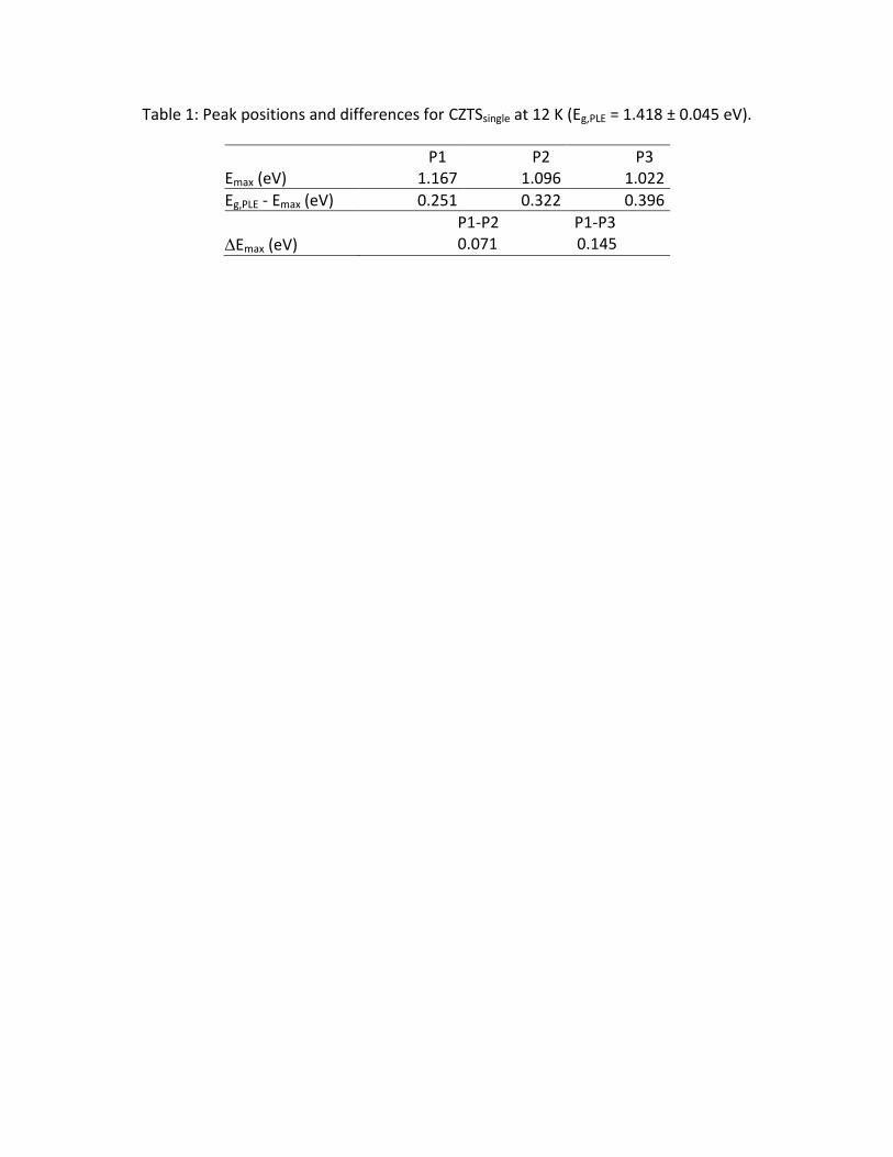
exciton band is not resolved, which confirms the presence of potential fluctuations in the material. The increase of the excitation spectrum intensity at the long wavelength side is related to the optical absorption spectrum but not identical to it, because the efficiency of the emission is also involved [23, 25]. The linear extrapolation of squared PLE (labelled as Eg,PLE) at 12 K is 1.418 ± 0.045 eV. The separations between Eg,PLE and the emission peak energies at 12 K are given in table 1. The differences are large (250 - 400 meV), indicating that rather deep defects are involved in the q-DAP transitions. In CIGS the shift between the PLE onset and PL maximum is smaller than 200 meV [18, 22, 23, 24, 25]. In figure 5b a clear decrease of the linear extrapolations of squared PLE as a function of temperature can be seen. The maximum of the PL peaks roughly follows the band gap shift. The red shift of the PL spectrum expected for q-DAP recombination with increasing temperature seems rather small. This might be related to the deep energetic position of the defects. This is in accordance with reference [8] which shows that the temperature dependence of the two peak positions follows more or less the temperature dependence of the band gap as calculated in reference [20]. The two PL bands showed a strong blue shift with increasing excitation power (15 meV/decade) and were explained by band-defect transitions involving the same deep acceptor (280 meV) but in different CZTS phases with a different band gap.
4 Discussion The low temperature PL spectra consist of three broad bands, that exhibit a large blue shift with increasing excitation power. This is typical for recombination in highly compensated semiconductors where potential fluctuations are present. Because of the relatively large spectral shift of the emission peaks from the band gap energy (Eg,PLE), q-DAP pair recombination seems the most probable PL mechanism. Two explanations for the occurrence of three PL peaks are evident: 1) q-DAP recombination between different defect pairs and 2) q-DAP recombination of one dominant defect pair in different phases of the polycrystalline absorber. As explained below, the experiments do not clearly favour one of these models, a combination of both may also be possible. For the first explanation, involving q-DAP recombinations between different defects, information about possible defects in CZTS is necessary. So far, in comparison with CIGS, considerably less experimental and computational efforts have been spent in determining formation energies and defect level positions in CZTS. Experimentally determined thermal activation energies are quite low 30-60 meV [3, 4, 5] compared to theoretical first principles calculations. These calculations [26, 27], however, do not completely agree on the nature of the dominant defects and the level positions they introduce in the CZTS band gap. There seems to be a consensus that CuZn antisites (Ea ≈ 120 meV [26], 220 meV [27]) and copper vacancies (VCu, Ea ≈ 20 meV [26], 70 meV [27]) are the dominant acceptor type defects, and that ZnCu antisites (Ea ≈ 150 meV [26], 70 meV [27]) and Cu interstitials (Cui, Ea ≈ 150 meV [26], 50 meV [27]) form rather shallow donors. In general, Ea for both donors and acceptors is larger than in CIGS [11, 28]. These large defect activation energies seem confirmed by the large shift between the band gap determined from PLE and the PL maxima in CZTS. At this moment, it seems not obvious to link the results for the observed three PL peaks to these theoretical predictions. The exact determination of the correct defect activation energy is hindered by: the dependence of the
peak position on excitation power, the unknown value of , the dependence on detection
energy in PLE measurements. Further experimental and computational studies are necessary to provide clarity into the origin of the donors and acceptors involved in the PL processes.
Alternatively, the occurrence of three peaks in the PL spectra can be explained by essentially the same q-DAP recombination mechanism in different phases in the absorber layer. The differences in peak energy between P2 and P1, and P3 and P1 (see Table 1) might, indeed, be related to the difference in band gap energy between the kesterite and disordered phase (0.04 eV [29]), and kesterite and stannite phase (0.12 eV [30] - 0.15 eV [31]), respectively. The structural difference between these phases lies in the arrangement of the Cu and Zn atoms, differently ordered for the kesterite and stannite phases, and random in the disordered phase. Kesterite is thermodynamically most stable, but as energy differences between the phases are small, it is very likely that the three phases can coexist [1]. If the peaks in the PL spectrum are assigned to a q-DAP transitions between the same, or very similar types of defects in three coexisting CZTS phases, one could consider that P3, P2 and P1 arise from stannite, the disordered phase and kesterite, respectively. An inhomogeneous distribution of these three CZTS phases may then explain the dependence of the PL spectrum on the excitation spot position on the sample. The complex phase diagram of Cu, Zn, Sn and S predicts the formation of still other phases during the absorber growth. In order to provide an explanation for the PL peaks, their PLE onset (band gap) must be around 1.3 eV. Possible candidates that are likely to be formed are tetragonal Cu2SnS3 (Eg ≈ 1.35 eV [32]) and SnS (Eg ≈ 1.3 eV [33]). The latter is normally found at the back contact of the cell. Unfortunately, information about the exact phase composition of the absorber is experimentally difficult to assess due to overlapping peaks in X-ray diffraction and Raman spectra.
5 Conclusions Photoluminescence spectroscopy has been performed to reveal the defect structure in Cu-poor, Zn-rich CZTS thin film solar cells, grown by reactive sputtering. Three peaks could be distinguished in the energy range from 0.9 -1.3 eV. The effect of potential fluctuations is clearly seen on the PL spectra, by a broadening of the peaks and a strong blue shift as excitation power increases. We were able to fit all spectra from two different cells, at different temperatures and excitation powers, with three Gaussian contributions. Via PLE measurements the energetic distance between the PL emission and band gap energy is estimated. As this distance is large, the involvement of deep defects is very likely. A complete explanation of the contributions in the PL spectra requires more information about basic defect properties in CZTS and about the phase composition of the absorber in these samples. The fact that the relative peak contributions exhibit considerable spatial differences strongly indicates that inhomogeneity in phase composition and/or defect distribution is important for these cells.
Acknowledgements The authors acknowledge the Special University Fund of UGent (BOF-01N01611) and Hercules Foundation (project AUGE/09/024 “Advanced Luminescence Setup") for financial support.
References
[1] S. Siebentritt and S. Schorr, Kesterites - a challenging material for solar cell, Prog. Photovoltaics 20 (2012) 512-519.
[2] T. Kato, H. Hiroi, N. Sakai, S. Muraoka and H. Sugimoto, Characterization of front and back interfaces on Cu2ZnSnS4 thin-film solar cells, Proc. 27th European Photovoltaic Solar Energy Conference and Exhibition, Frankfurt (2012) 2236-2239.
[3] Y. Miyamoto, K. Tanaka, L. Oonuki, N. Moritake and H. Uchiki, Optical properties of Cu2ZnSnS4 thin films prepared by sol-gel and sulfurization method, Jpn. J. Appl. Phys. 47 (2013) 596-597.
[4] J. P. Leitão, N. M. Santos, P. A. Fernandes, P. M. P. Salomé, A. F. da Cunha, J. C. González, G. M. Ribeiro and F. M. Matinaga, Photoluminescence and electrical study of fluctuating potentials in Cu2ZnSnS4-based thin films, Phys. Rev. B. 84 (2011) 024120
[5] K. Tanaka, Y. Miyamoto, H. Uchiki, K. Nakazawa and H. Araki, Donor-acceptor pair recombination luminescence from Cu2ZnSnS4 bulk single crystals, Phys. stat. sol. 203 (2006) 2891-2896.
[6] H. Yoo, J. Kim and L. Zhang, Sulfurization temperature effects on the growth of Cu2ZnSnS4 thin film, Current Applied Physics 12 (2012) 1052-1057.
[7] M. A. M. Khan, S. Kumar, M. Alhoshan and A. S. Al Dwayyan, Spray pyrolysed Cu2ZnSnS4 absorbing layer: A potential candidate for photovoltaic applications, Optics and Laser Technology 49 (2013) 196-201.
[8] M. Grossberg, J. Krustok, J. Raudoja and T. Raadik, The role of structural properties on deep defect states in Cu2ZnSnS4 studied by photoluminescence spectroscopy, Appl. Phys. Lett. 101 (2012) 102102
[9] D. Abou-Ras, T. Kirchartz and U. Rau, Advanced Characterization Techniques for Thin Film Solar Cells, first ed., Wiley, Weinheim, 2011.
[10] K. Hönes, E. Zscherper, J. Scragg and S. Siebentritt, Shallow defects in Cu2ZnSnS4, Physica B 404 (2009) 4949 -4952.
[11] S. Siebentritt and U. Rau, Wide-Gap Chalcopyrites, first ed., Springer, Berlin, 2006.
[12] S. A. Schumacher and J. R. Botha, Photoluminescence study of potential fluctuations in thin layers of Cu(In0.75Ga0.25)(SySe1-y)2, J. Appl. Phys. 99 (2006) 063508
[13] P. W. Yu, Excitation-dependent emission in Mg-, Be-, Cd-, and Zn-implanted GaAs, J. Appl. Phys. 48 (1977) 5043-5041.
[14] V. V. Osipov, T. I. Soboleva and M. G. Foigel, Impurity radiative recombination in heavily doped semiconductors, Sov. Phys. Semicond. 11 (1977) 752-758.
[15] T. Ericson, J. J. Scragg, A. Hultqvist, T. Wätjen, P. Szaniawski, T. Törndahl and C. Platzer-Björkman, Zn(O,S) buffer layers and thickness variations of CdS buffer for Cu2ZnSnS4 solar cells, Journal of Photovoltaics 4 (2014) 465-469.
[16] A. Bauknecht, S. Siebentritt, J. Albert and M. Ch. Lux-Steiner, Radiative recombination via intrinsic defects in CuxGaySe2, J. Appl. Phys. 89 (2001) 4391-4400.
[17] A. Bauknecht, S. Siebentritt, A. Gerhard, W. Harneit, S. Brehme, J. Albert, S. Rushworth and M. Ch. Lux-Steiner, Defects in CuGaSe2 thin films grown by MOCVD, Thin Solid Films 361 (2000) 426-431.
[18] H. Zachmann, S. Puttnins, M. V. Yakushev, F. Luckert, R. W. Martin, A. V. Karotki, V. F. Gremenok and A. V. Mudryi, Fabrication and characterisation of Cu(In,Ga)Se2 solar cells on polyimide, Thin Solid Films 519 (2011) 7264-7267.
[19] I. Dirnstorfer, D. M. Hofmann, D. Meister, B. K. Meyer, W. Riedl and F. Karg, Postgrowth thermal treatment of CuIn(Ga)Se2: Characterization of doping levels of In-rich thin films J. Appl. Phys. 85 (1999) 1423-1428.
[20] P. Sarswat and M. L. Free, A study of energy band gap versus temperature for Cu2ZnSnS4 thin films, Physica B 407 (2012) 108-111.
[21] A. P. Levanyuk and V. V. Osipov, Edge luminescence of direct-gap semiconductors, Sov. Phys. Usp. 24 (1981) 187-215.
[22] J. Krustok, J. Raudoja, M. Yakushev, R. D. Pilkington and H. Collan, On the shape of the close-to-band-edge photoluminescent emission spectrum in compensated CuGaSe2, Phys. stat. sol. a 173 (1999) 483-490.
[23] I. Dirnstorfer, M. Wagner, D. M. Hofmann, M. Lampert, F. Karg and B. Meyer, Characterization of CuIn(Ga)Se2 Thin Films; In-rich layers Phys. stat. sol. 168 (1998) 163-175.
[24] H. Zachmann, S. Heinker, A. Braun, A. V. Mudryi, V. F. Gremenok, A. V. Ivaniukovich and M. V. Yakushev, Characterisation of Cu(In,Ga)Se2-based thin film solar cells on polyimide, Thin Solid Films 517 (2009) 2209-2212. [25] S. Siebentritt, N. Papathanasiou and M. Lux-Steiner, Photoluminescence excitation spectroscopy of highly compensated CuGaSe2, Phys. stat. sol. b 242 (2005) 2627-2632.
[26] S. Chen, J. Yang, X. G. Gong, A. Walsh and S. Wei, Intrinsic point defects and complexes in
the quaternary kesterite semiconductor Cu2ZnSnS4, Phys. Rev. B 81 (2010) 245204.
[27] D. Han, Y. Y. Sun, J. Bang, Y. Y. Zhang, H. Sun, X. Li and S. B. Zhang, Deep electron traps and origin of p-type conductivity in the earth-abundant solar-cell material Cu2ZnSnS4, Phys. Rev. B 87 (2013) 155206.
[28] S. B. Zhang, S. Wei and A. Zunger, Defect physics of the CuInSe2 chalcopyrite semiconductor, Phys. Rev. B 57 (1998) 9642-9657.
[29] S. Chen, X. G. Gong, A. Walsh and S. Wei, Crystal and electronic band structure of Cu2ZnSnX4 (X = S and Se) photovoltaic absorbers: First-principles insights, Appl. Phys. Lett. 94 (2009) 041903.
[30] J. J. Scragg, Copper Zinc Tin Sulfide Thin Films for Photovoltaics, first ed., Springer, Berlin, 2011.
[31] A. Walsh, S. Chen, S. Wei and X. Gong, Kesterite thin-film solar cells: advances in materials modelling of Cu2ZnSnS4, Adv. Energy Mater. 2 (2012) 400-409.
[32] P. A. Fernandes, M. P. Salomé and A. F. da Cunha, CuxSnSx-1 (x = 2, 3) thin films grown by sulfurization of metallic precursors deposited by dc magnetron sputtering, Phys. Status Solidi C 7 (2010) 901-904.
[33] C. Cifuentes, M. Botero, E. Romero, C. Calder and C. Gordillo, Optical and structural studies on SnS films grown by co-evaporation, Braz. J. Phys. 36 (2006) 1046-1049.
Figures
Figure 1: SEM images (a) CZTSsingle, (b) CZTSdouble
Figure 2: Normalized EQE spectra show the effect of a double CdS buffer at the short
wavelength side.
Figure 3: (a) Comparison of CZTSsingle and CZTSdouble PL spectra (T= 10 K, exci = 550 nm), (b) fit at normalized spectra of two sample positions for CZTSdouble showing the same peaks (T= 10 K,
exci = 500 nm).
400 600 800 1000
0
0.2
0.4
0.6
0.8
1.0
(nm)
EQE
(arb
. un
its)
single
double
0.9 1.0 1.1 1.2 1.30
0.2
0.4
0.6
0.8
1.0
E (eV)
double1double2
0.9 1.0 1.1 1.2 1.30
0.2
0.4
0.6
0.8
1.0
E (eV)
No
rmal
ize
d in
ten
sity
single
double
(a) (b)
P1P2
P3
Figure 4: Emission peak energy for P1 and P2 as a function of excitation power for CZTS single
(exci = 500 nm, T= 5 K).
Figure 5: (a) Temperature dependence of PL and PLE for CZTSsingle, the arrow indicates
temperature decrease from 12 to 62 K, (b) Eg,PLE and peak maximum P1 and P2 as a function of temperature.
101
102
1.00
1.05
1.10
1.15
1.20
Relative excitation power
Ep
ea
k (
eV
)
P1
P2
700 900 1100 13000
1
2
3
4
5
x 104
(nm)
Inte
nsi
ty (
cou
nts
/s)
0 20 40 60 80 100
1.0
1.1
1.2
1.3
1.4
1.5
T (K)
E (e
V)
PLE PL
P1
P2
(b)(a)
g,PLEE
T
Table 1: Peak positions and differences for CZTSsingle at 12 K (Eg,PLE = 1.418 ± 0.045 eV).