44
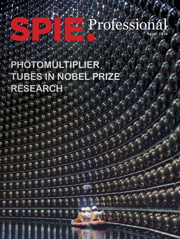
April 2016 PHOTOMULTIPLIER TUBES IN NOBEL PRIZE RESEARCH
April 2016
PHOTOMULTIPLIER TUBES IN NOBEL PRIZE RESEARCH
Laser and Physical Optics Design SoftwareGLAD
International Distributors: FIT Leadintex, Inc., Japantel: 81 3 3666 7100, [email protected], Shanghai, tel: +86-21-64860708, [email protected]
Applied Optics Research tel: 1 360 225 9718, fax: 1 360 225 0347 e-mail: [email protected], www.aor.com
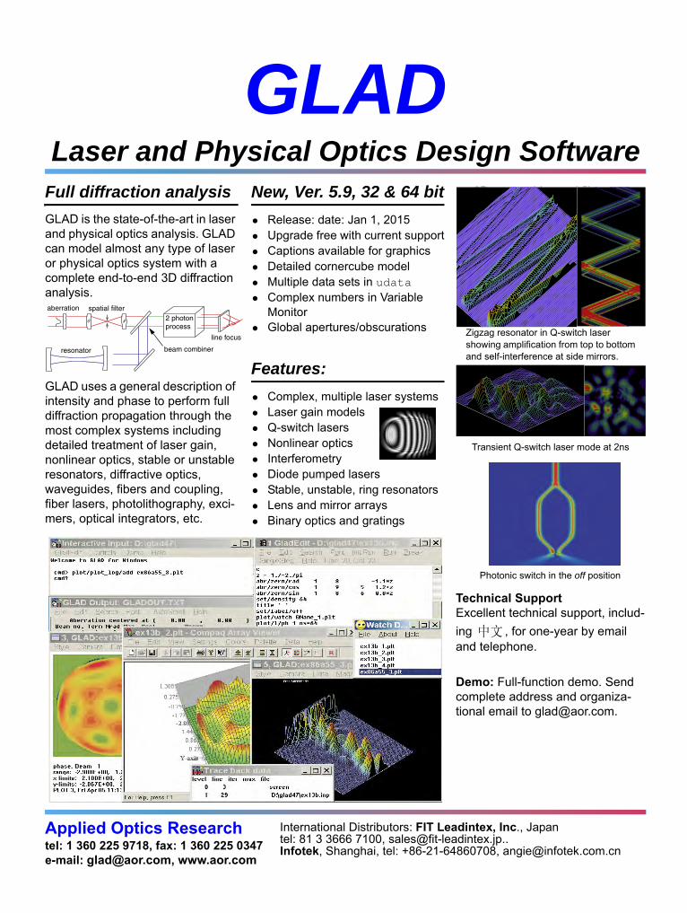
Full diffraction analysisGLAD is the state-of-the-art in laser and physical optics analysis. GLAD can model almost any type of laser or physical optics system with a complete end-to-end 3D diffraction analysis.
GLAD uses a general description of intensity and phase to perform full diffraction propagation through the most complex systems including detailed treatment of laser gain, nonlinear optics, stable or unstable resonators, diffractive optics, waveguides, fibers and coupling, fiber lasers, photolithography, exci-mers, optical integrators, etc.
resonator
aberration spatial filter2 photon process
line focus
beam combiner
New, Ver. 5.9, 32 & 64 bit• Release: date: Jan 1, 2015• Upgrade free with current support• Captions available for graphics• Detailed cornercube model• Multiple data sets in udata • Complex numbers in Variable
Monitor• Global apertures/obscurations
Features:• Complex, multiple laser systems• Laser gain models• Q-switch lasers• Nonlinear optics• Interferometry• Diode pumped lasers• Stable, unstable, ring resonators• Lens and mirror arrays• Binary optics and gratings
• 3D waveguides and fibers
Zigzag resonator in Q-switch laser showing amplification from top to bottom and self-interference at side mirrors.
Photonic switch in the off position
Technical SupportExcellent technical support, includ-ing , for one-year by email and telephone.
Demo: Full-function demo. Send complete address and organiza-tional email to [email protected].
Transient Q-switch laser mode at 2ns

1APRIL 2016 | SPIE Professional
Volume 11, Number 2 (ISSN 1817-4035)
Features
Send returns and materials to SPIE Professional, P.O. Box 10, Bellingham, WA 98227-0010 USA.
3 President’s LetterSPIE President Robert Lieberman discusses the mythical gap between academia and industry.
INDUSTRY 4 Prism Awards
Nine new innovative products honored.
6 SPIE Startup Challenge 3D imaging system wins Startup Challenge.
7 US revising export rules 8 Conflict minerals
Are the disclosure rules working?
11 Canada photonics industry report A new report says Canadian photonics is at a tipping point.
12 AIM Photonics The new US manufacturing institute has lofty goals.
15 Solar market insights
PHOTONICS FOR A BETTER WORLD 16 Disease monitoring with Kinect
Microsoft and Novartis team up to help medically assess patients with multiple sclerosis.
TECHNOLOGY R&D 17 Recommended reading
Article in Optical Engineering examines the imaging chain.
18 Highlights from Photonics West Record-breaking participation in San Francisco.
20 Photomultiplier tubes Neutrino research using Hamamatsu Photonics’ photomultiplier tubes wins 2015 Nobel Prize.
24 BiOS highlights Cancer-fighting technologies take center stage.
25 Gravitational wavesA new field of gravitational-wave astronomy is born.
INTERNATIONAL YEAR OF LIGHT 2015 26 IYL continues massive reach
MEMBERSHIP 28 SPIE Frits Zernike Award
SPIE Fellow Yan Borodovsky receives SPIE microlithography award.
29 SPIE election and award nominationsUpcoming SPIE elections.
29 The value of proceedings 30 New SPIE Fellows
Congratulations to the new class of SPIE Fellows.
CAREER 32 Weathering a career change
Two seemingly separate careers come together in the UK.
34 SPIE salary survey The 2016 SPIE salary report of the optics and photonics industry.
EVENTS 36 SPIE Optics + Photonics37 SPIE Translational Biophotonics 38 SPIE Defense + Commercial Sensing 39 Astronomical Telescopes + Instrumentation40 Events Around the World
Cover and above photo: Workers inspect 20-inch photomultiplier tubes inside the Super-Kamiokande detector. © Kamioka Observatory, Institute for Cosmic Ray Research, University of Tokyo.

© 2016 Society of Photo-Optical Instrumentation Engineers (SPIE). All rights reserved. The articles published in SPIE Professional reflect the work and thoughts of the authors. Every effort has been made to publish reliable and accurate information herein, but the publisher is not responsible for the validity of the information or for any outcomes resulting from reliance thereon. Inclusion of ar-ticles and advertisements in this magazine does not necessarily constitute endorsement by the editors or SPIE. The magazine accepts no respon-sibility for unsolicited manuscripts or artwork; they will not be returned unless accompanied by a stamped, self-addressed envelope.Send returns and materials to SPIE Professional, P.O. Box 10, Bellingham, WA 98227-0010 USA.
The Member Magazine of SPIEspie.org/spieprofessional
Managing EditorKathy [email protected]+1-360-685-5538
Graphic ArtistCarrie Binschus
ContributorsJacqueline Andreozzi, Carrie Binschus, Andrew Brown, Stacey Crockett, Rich Donnelly, Andy Extance, Peter Hallett, Mike Hatcher, Christine Hosler, Eddie Jacobs, Kathy Kincade, Tim Lamkins, Amy Nelson, Matt Peach, Courtney Rambo, Adam Resnick, Kathy Sheehan, Karen Thomas, Khushi Vyas, Chris Warner, Gerald Wong, and Marcus Woo.
Editorial Advisory BoardJames G. Grote, chair, US Air Force Research Lab; Kristen Carlson Maitland, Texas A&M University; Jason M. Eichenholz, Open Photonics
2016 SPIE PresidentRobert A. Lieberman
SPIE CEOEugene G. Arthurs
SPIE Director of Education and Community ServicesKrisinda Plenkovich
SPIE Director of PublicationsEric Pepper
Advertising SalesMelissa [email protected]+1-360-685-5596
Volume 11, Number 2 SPIE Professional (ISSN 1817-4035) is publish ed quarterly by SPIE, 1000 20th St., Bellingham, WA 98225-6705 USA.
TFCalc Optical Coating Design Software
Software Spectra, Inc. Phone: (800) 832-2524 • Fax: (503) 690-8159Web: www.sspectra.com • E-mail: [email protected]
TFCalc 3.6 is a powerful, but easy to use, tool for designing / modeling / analyzing / manufacturing thin film structures. Some of its many features are listed below
• absorption • active layers• angle matching • animation • bandpass filter design • biconical transmittance • blackbody illuminant • color optimization • cone-angle optimization• constraints • continuous targets • derivative targets • detectors • dispersion formulas
• DLL available • electric field intensity • equivalent index • equivalent stack • gain materials • global optimization • group optimization • illuminants• interactive analysis • layer sensitivity • local optimization • material mixtures • multiple processor support • needle optimization
• optical monitoring • optical density • phase shift • delta and psi • radiation distributions • refractive index determination • sensitivity analysis • stack formula • synthesis • tunneling • ultra-fast quantities • variable materials• WDM module • yield analysis
SPIE Professional is accepting article proposals.Future issues of the open-access magazine will cover career and industry topics as well as advances in interferometers, light bulbs, quantum devices, high-power lasers, and more.Please submit your idea as a short outline or abstract to:
Call for Articles
PRESIDENT’S LETTER
Is there really a gap between basic research and commercialization?
The work of 60,000 annual contributors to SPIE events, journals, and other activities covers electromagnetic wavelengths from
millimeters to Angstroms, and our professional undertakings cover a similarly broad spectrum. There is no better illustration of this than the wide variety of activities at SPIE meetings. First-time presenters and plenary speakers, authors and journal editors, session chairs and symposium chairs, members of all grades, and trade show exhibitors engage in every aspect of optics and photonics at these meetings. This broad range covered by the optics and photonics profession and our Society becomes most obvious at SPIE Photonics West where there were more than 22,000 registrations, a record. Representatives from industry, government, universities, and even high schools came to San Francisco to bridge the barriers between scientific disciplines, between basic research and applied engineering, and between invention and commercialization.
ACADEMIA AND INDUSTRY TOGETHER Conference rooms brimmed with medical doctors, biochemists, biophysicists, physical chemists, materials scientists, device design engineers, solid-state physicists, and multidisciplinary scientists who mine the fertile interstices between traditional fields of study. Papers on fundamental breakthroughs in laser science, optoelectronics, and biophotonics shared screens with translational research on medical diagnostics and other technologies, and with reports on the performance of prototype devices and systems of all kinds. The SPIE Startup Challenge, workshops on product development and funding strategies, forums on government trade regulations, and presentation of the world-recognized Prism Awards for Photonics Innovation spanned the continuum of photonics business development activities. Networking events and committee meetings brought together a full spectrum of important groups, ranging from SPIE Women in Optics, photonics industry clusters, and student leaders to those interested in public policy, publishing, and photonics for the developing world. And of course, the Photonics West exhibition and BiOS Expo were filled with hundreds and hundreds of light-related companies of all types and sizes, from around the world.
CONTINUA OF OPTICS AND PHOTONICS Throughout the year, SPIE contributors engage in the full spectrum of activities evident at Photonics West. Whether in San Diego, San Francisco, Baltimore, Brussels or Beijing, the energy of people working to advance our field is unflagging. New discoveries, new applications, new products, and even new companies are generated by the very human interactions between people who get together to discuss their results and learn from others. Ongoing collaborations coordinated by the SPIE professional staff in the USA and UK provide opportunities for people at all levels, and from any continent, to support these activities even when it is inconvenient to attend every relevant meeting. Because we deal with the optical spectrum every day, it is easy for people in our field to bridge “gaps” that others sometimes stumble over. Here are two examples: Where some might see no relationship between telecommunications and surgery, we clearly see that lasers (different types, working at different wavelengths, but still lasers) have revolutionized both fields. Similarly, the current worldwide trend to more closely tie scientific research to activities that will directly benefit humanity and promote socioeconomic welfare is a bit unsettling to some scientists, but it’s “old news” to most of us. We know from working with light that there is no real gap between basic research and product development: These activities are just two ends of a fascinating continuum! .
Robert A. Lieberman 2016 SPIE President
Optics, photonicscan help achieve UN sustainabledevelopment goals
World leaders adopted 17 goals for sustainable development at the UN Sustainable Development summit in September 2015.
Optics and photonics are important tools for achieving these goals, especially those aimed at ending poverty and hunger and improving health and quality education.
A new SPIE poster illustrates ways in which SPIE members can join in the UN agenda to achieve these goals by 2030.
For a free copy, email [email protected].
3APRIL 2016 | SPIE Professional
Because we deal with the optical spectrum every day, it is easy for people in our field to bridge “gaps” that others sometimes stumble over.
INDUSTRY
DETECTORS & SENSORS
BIOMEDICAL INSTRUMENTATION
DISPLAYS & LIGHTING
Spectral Engines (Finland)The Wireless IR Analyzer is a miniaturized and robust infrared spectrometer capable of covering infrared ranges above 1.7 µm without any loss in performance. The central element in this resilient IR spectrometer is a novel monolithic, off-plane micromechanical Fabry-Perot interferometer enabling fast and stable operation and resistance to shocks, vibrations, and wear. Unlike conventional spectrometers, the spectral sensor does not have a slit or folding optics. It only requires a single point detector instead of a linear array, allowing simple direct optics and a high throughput. Integrated data-analysis algorithms and a Bluetooth connection make this device an IR spectroscopic lab in your pocket.
Biodesy (USA)Biodesy Delta delivers real-time protein analysis with greater sensitivity, lower cost, and high throughput. Proteins are the workhorses of the body, and Biodesy’s technology measures structural changes in proteins in real time. Structural information is critical to understanding the function or dysfunction of a protein and the mechanism of action of a drug targeted to that protein. Using an ultrafast mode-locked Ti:S laser that excites the second harmonic generation signal, Delta analyzes protein structures in motion in their native environment. Liquid-handling robotics and a custom 384-well microplate with integrated prism optics, proprietary reagents, and software make this optical system perfect for enabling drug discovery.
Dolby, Christie, Necsel (USA)The Dolby Vision Cinema Laser Projector was created by Necsel, Dolby, and Christie for a greatly enhanced premium cinema experience with high contrast, high brightness, a wide color gamut, and excellent 3D performance. Necsel developed new laser wavelengths to enable the six color–based 3D as well as new laser integration techniques for the fiber-coupling used in the projector. Christie created a new projector architecture, utilizing Texas Instruments’ DLP cinema technology that enables contrast of greater than 1,000,000:1. Dolby provided high dynamic range expertise and new 3D glasses (using six primary colors) to accommodate the laser primaries and generate the 3D separation. At the systems level, the photonics are backed up by sophisticated software and electronics for image processing.
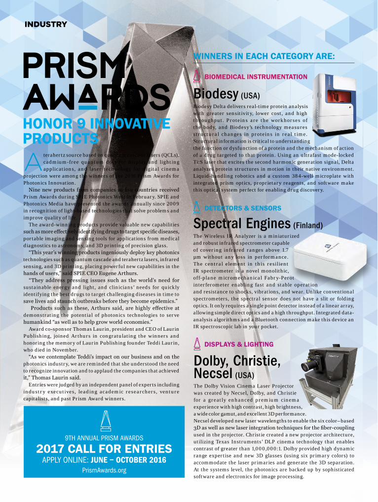
HONOR 9 INNOVATIVE PRODUCTS
WINNERS IN EACH CATEGORY ARE:
A terahertz source based on quantum cascade lasers (QCLs), cadmium-free quantum dots for display and lighting applications, and laser technology for digital cinema
projection were among the winners of the 2016 Prism Awards for Photonics Innovation. Nine new products from companies in five countries received Prism Awards during SPIE Photonics West in February. SPIE and Photonics Media have presented the awards annually since 2009 in recognition of light-based technologies that solve problems and improve quality of life. The award-winning products provide valuable new capabilities such as more effectively identifying drugs to target specific diseases, portable imaging and sensing tools for applications from medical diagnostics to astronomy, and 3D printing of precision glass. “This year’s winning products ingeniously deploy key photonics technologies such as quantum cascade and terahertz lasers, infrared sensing, and 3D printing, placing powerful new capabilities in the hands of users,” said SPIE CEO Eugene Arthurs. “They address pressing issues such as the world’s need for sustainable energy and light, and clinicians’ needs for quickly identifying the best drugs to target challenging diseases in time to save lives and staunch outbreaks before they become epidemics.” Products such as these, Arthurs said, are highly effective at demonstrating the potential of photonics technologies to serve humankind “as well as to help grow world economies.” Award co-sponsor Thomas Laurin, president and CEO of Laurin Publishing, joined Arthurs in congratulating the winners and honoring the memory of Laurin Publishing founder Teddi Laurin, who died in November. “As we contemplate Teddi’s impact on our business and on the photonics industry, we are reminded that she understood the need to recognize innovation and to applaud the companies that achieved it,” Thomas Laurin said. Entries were judged by an independent panel of experts including industry executives, leading academic researchers, venture capitalists, and past Prism Award winners.
9TH ANNUAL PRISM AWARDS
2017 CALL FOR ENTRIES APPLY ONLINE: JUNE – OCTOBER 2016
PrismAwards.org
INDUSTRY
OPTICS & OPTICAL COMPONENTS
SCIENTIFIC LASERS
IMAGING & CAMERAS
OTHER METROLOGY INSTRUMENTATIONINDUSTRIAL LASERS
MATERIALS & COATINGS
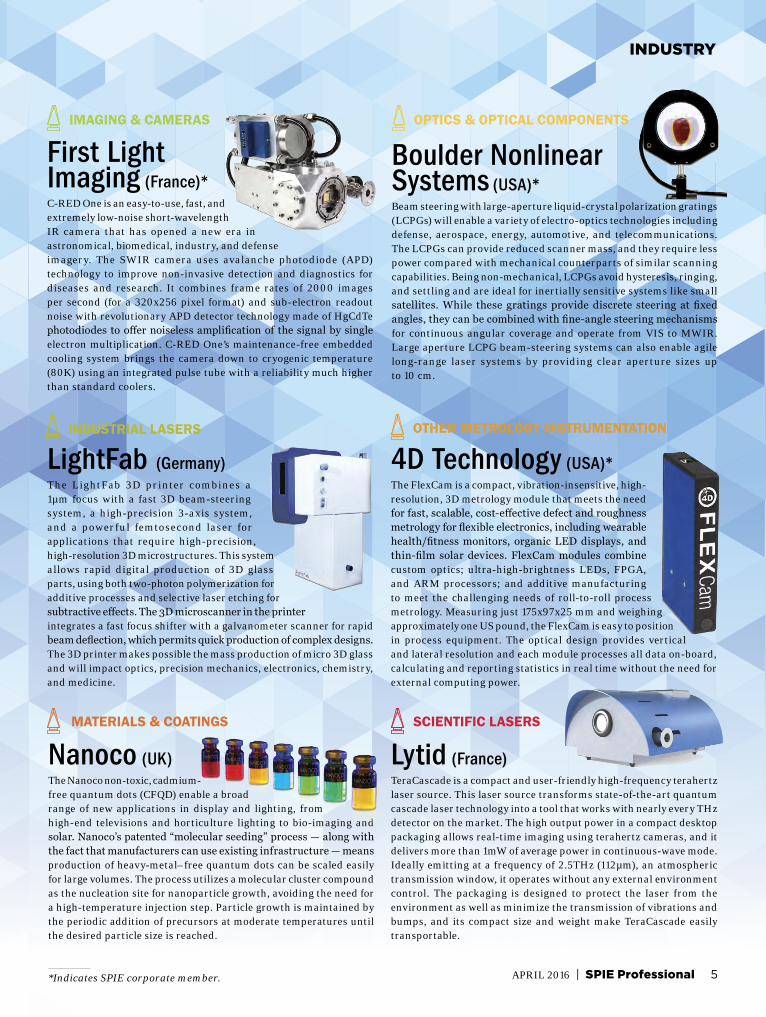
First Light Imaging (France)*C-RED One is an easy-to-use, fast, and extremely low-noise short-wavelength IR camera that has opened a new era in astronomical, biomedical, industry, and defense imagery. The SWIR camera uses avalanche photodiode (APD) technology to improve non-invasive detection and diagnostics for diseases and research. It combines frame rates of 2000 images per second (for a 320x256 pixel format) and sub-electron readout noise with revolutionary APD detector technology made of HgCdTe photodiodes to offer noiseless amplification of the signal by single electron multiplication. C-RED One’s maintenance-free embedded cooling system brings the camera down to cryogenic temperature (80K) using an integrated pulse tube with a reliability much higher than standard coolers.
Nanoco (UK) The Nanoco non-toxic, cadmium-free quantum dots (CFQD) enable a broad range of new applications in display and lighting, from high-end televisions and horticulture lighting to bio-imaging and solar. Nanoco’s patented “molecular seeding” process — along with the fact that manufacturers can use existing infrastructure — means production of heavy-metal–free quantum dots can be scaled easily for large volumes. The process utilizes a molecular cluster compound as the nucleation site for nanoparticle growth, avoiding the need for a high-temperature injection step. Particle growth is maintained by the periodic addition of precursors at moderate temperatures until the desired particle size is reached.
LightFab (Germany)The LightFab 3D printer combines a 1µm focus with a fast 3D beam-steering system, a high-precision 3-axis system, and a powerful femtosecond laser for applications that require high-precision, high-resolution 3D microstructures. This system allows rapid digital production of 3D glass parts, using both two-photon polymerization for additive processes and selective laser etching for subtractive effects. The 3D microscanner in the printer integrates a fast focus shifter with a galvanometer scanner for rapid beam deflection, which permits quick production of complex designs. The 3D printer makes possible the mass production of micro 3D glass and will impact optics, precision mechanics, electronics, chemistry, and medicine.
Boulder Nonlinear Systems (USA)*Beam steering with large-aperture liquid-crystal polarization gratings (LCPGs) will enable a variety of electro-optics technologies including defense, aerospace, energy, automotive, and telecommunications. The LCPGs can provide reduced scanner mass, and they require less power compared with mechanical counterparts of similar scanning capabilities. Being non-mechanical, LCPGs avoid hysteresis, ringing, and settling and are ideal for inertially sensitive systems like small satellites. While these gratings provide discrete steering at fixed angles, they can be combined with fine-angle steering mechanisms for continuous angular coverage and operate from VIS to MWIR. Large aperture LCPG beam-steering systems can also enable agile long-range laser systems by providing clear aperture sizes up to 10 cm.
4D Technology (USA)*The FlexCam is a compact, vibration-insensitive, high-resolution, 3D metrology module that meets the need for fast, scalable, cost-effective defect and roughness metrology for flexible electronics, including wearable health/fitness monitors, organic LED displays, and thin-film solar devices. FlexCam modules combine custom optics; ultra-high-brightness LEDs, FPGA, and ARM processors; and additive manufacturing to meet the challenging needs of roll-to-roll process metrology. Measuring just 175x97x25 mm and weighing approximately one US pound, the FlexCam is easy to position in process equipment. The optical design provides vertical and lateral resolution and each module processes all data on-board, calculating and reporting statistics in real time without the need for external computing power.
Lytid (France)TeraCascade is a compact and user-friendly high-frequency terahertz laser source. This laser source transforms state-of-the-art quantum cascade laser technology into a tool that works with nearly every THz detector on the market. The high output power in a compact desktop packaging allows real-time imaging using terahertz cameras, and it delivers more than 1mW of average power in continuous-wave mode. Ideally emitting at a frequency of 2.5THz (112µm), an atmospheric transmission window, it operates without any external environment control. The packaging is designed to protect the laser from the environment as well as minimize the transmission of vibrations and bumps, and its compact size and weight make TeraCascade easily transportable.
5APRIL 2016 | SPIE Professional*Indicates SPIE corporate member.
6 SPIE Professional | APRIL 2016
INDUSTRY
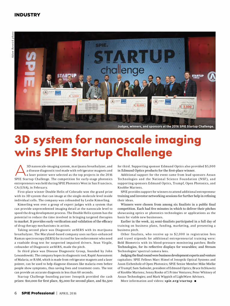
3D system for nanoscale imaging wins SPIE Startup Challenge
A 3D nanoscale-imaging system, marijuana breathalyzer, and a disease diagnostic tool made with refrigerator magnets and a laser pointer were selected as the top projects in the 2016
SPIE Startup Challenge. The competition for early-stage photonics entrepreneurs was held during SPIE Photonics West in San Francisco, CA (USA), in February. First-place winner Double Helix of Colorado won the grand prize with its 3D system that can image at the single-molecule level inside individual cells. The company was cofounded by Leslie Kimerling. Kimerling won over a group of expert judges with a system that can provide unprecedented imaging detail at the nanoscale level to speed the drug development process. The Double Helix system has the potential to reduce the time involved in bringing targeted therapies to market. It provides early verification and validation of the efficacy of drug therapy mechanisms in action. Taking second place was Diagnostic anSERS with its marijuana breathalyzer. The Maryland-based company uses surface-enhanced Raman spectroscopy (SERS) for its tool for law enforcement who need a roadside drug test for suspected impaired drivers. Sean Virgile, cofounder of Diagnostic anSERS, made the pitch. In third place was Disease Diagnostic Group, founded by John Lewandowski. The company hopes its diagnostic tool, Rapid Assessment of Malaria, or RAM, which is made from refrigerator magnets and a laser pointer, can be used to help diagnose diseases like malaria even before people show symptoms, thus saving lives and treatment costs. The test can provide an accurate diagnosis in less than 60 seconds. Startup Challenge founding partner Jenoptik provided the cash prizes: $10,000 for first place, $5,000 for second place, and $2,500
for third. Supporting sponsor Edmund Optics also provided $5,000 in Edmund Optics products for the first-place winner. Additional support for the event came from lead sponsors Axsun Technologies and the National Science Foundation (NSF), and supporting sponsors Edmund Optics, Trumpf, Open Photonics, and Knobbe Martens. SPIE provides support for winners to attend additional entrepreneur training and investor networking sessions for further help in refining their ideas. Winners were chosen from among six finalists in a public final competition. Each had five minutes in which to deliver their pitches showcasing optics or photonics technologies or applications as the basis for viable new businesses. Earlier in the week, 25 semi-finalists participated in a full day of training on business plans, funding, marketing, and presenting a business pitch. Other finalists, who receive up to $2,000 in registration fees and travel stipends for additional entrepreneurial training were: Bold Biometrix with its blood-pressure monitoring patches; Bodle Technologies, for its reflective displays for wearables; and Stream Technologies’ spectral camera lens. Judging the final round were business development experts and venture capitalists: SPIE Fellows Marc Himel of Jenoptik Optical Systems and Jason Eichenholz of Open Photonics; SPIE Senior Member Mike Mielke of Trumpf; Sam Sadoulet, president of Edmund Optics; Bruce Itchkawitz of Knobbe Martens; Jenny Rooke of 5 Prime Ventures; Peter Whitney of Axsun Technologies; and Mark Wippich of LightWave Advisors. More information and videos: spie.org/startup .
Judges, winners, and sponsors at the 2016 SPIE Startup Challenge.
Adam
Res
nick
pho
to
7APRIL 2016 | SPIE Professional
INDUSTRY
US revising export rules The comment period will close 4 April for the second proposed
rule for US export regulations covering a wide range of key photonics products and technologies.
The proposed changes are the second set of revisions proposed for the Commerce Control List (CCL) and Category XII of the US Munitions List (USML), which govern many of the optics and photonics commodities covered by International Traffic in Arms Regulations (ITAR) and Export Administration Regulations. The rewrite is part of the overarching Export Control Reform initiative undertaken by the Obama Administration. Although the new proposal is a significant improvement from the rules proposed in May 2015, SPIE has asked companies and universities to still review the proposals carefully for potential impacts, including the Department of Commerce rule, which establishes controls for items moving from the USML to the CCL. “The changes will have direct and lasting impact on industry and our academic community,” said SPIE CEO Eugene Arthurs. “Our industry is often described as fragmented because of the myriad of small- and medium-sized enterprises with unique expertise serving niches that are extraordinarily deep technically. The overhead burden for export-control compliance is a challenge
to these businesses and to university research laboratories where covered products are used or developed. Well-written regulations that are limited to our highest priorities for control are key to reducing that burden,” he said. Historically, he said, the US export-control system has fostered an environment where non-US companies with similar products are selling freely — and using the motto “ITAR-Free” to do so. “These companies are prudently investing the resulting revenue back into their companies, enabling rapid growth,” Arthurs noted. “This scenario comes at the detriment of the US industry’s growth and the high-paying jobs that come with it. More work will always be needed as our industry constantly changes and grows, but it is our hope at SPIE that a final rule will lead US export controls in a more positive direction.” This second proposed rule utilizes the “specially designed” criteria in many areas, which was a request from industry and SPIE during the 2015 comment period. Jennifer Douris, government affairs director for SPIE, explained that the “specially designed” criteria, which entails a formal review process, “helps ensure that dual-use components are not considered munitions items.” More information, including slides and audio from the 2 March SPIE webinar on this issue: spie.org/export .
C U S T O M M A N U FA C T U R E R O F P R E C I S I O N O P T I C S : M E D I C A L • D E F E N S E • S C I E N T I F I C • A S T R O N O M Y • I N D U S T R I A L
Batesville, Arkansas
Attention to detail of the highest order. Fiercely attentive customer service. Exceptional craftsmanship.
Wrapped in the experience of a little over 68 years. www.lacroixoptical.com.
It’s the little things that matter.

8 SPIE Professional | APRIL 2016
CONFLICT MINERAL RULES: Are they
working?
A miner in Kailo, DRC, with some wolframite, the mineral source of tungsten.
Phot
o: J
ulie
n H
arne
is
View an SPIE Newsroom video about conflict minerals: spie.org/minerals
9APRIL 2016 | SPIE Professional
INDUSTRY
Efforts to curtail violence in Africa by tracing the origin of key metals used in optoelectronics are ongoing, despite interruption from a legal challenge.
By Andy Extance
regulation will be issued around the middle of 2016.” If the EU does adopt its own rules, that will greatly expand the number of companies that actively gather and provide information, she says. “Over time, more of their customers will probably have a ‘DRC conflict-free’ policy or goal, and optoelectronics companies will need to have visibility throughout their supply chains in order to qualify as suppliers,” Thomas says. Rosemarie Szostak, senior analyst at the research and advisory firm Nerac, has been working to help companies meet the SEC’s regulations. She emphasizes that full compliance would call for great vigilance and cost because of the ubiquity of 3TG metals in many electronics products and processes. Gold coatings for mirrors and gratings are a common application of conflict metals in optoelectronics, she notes. Tin is used as a solder in mounting devices, and tantalum is also important in the manufacture of capacitors.
DODD-FRANK REPORTING REQUIREMENTS The rule’s relevance to optoelectronics can be seen in the conflict-minerals reports from Avago Technologies in California (USA). Selling a variety of relevant products, including LEDs and fiber-optic components and subsystems, Avago’s conflict-minerals policy focuses on checking its suppliers’ sources of 3TG minerals. “We do not typically have a direct relationship with 3TG smelters and refiners,” the company writes. “Avago’s relevant suppliers are required to implement measures to prohibit the purchase and use of conflict minerals” from the DRC and adjoining countries that “fund
armed conflict in those countries.” In December 2013, that involved querying 188 suppliers, who together made 3251 references to a total of 383 smelters and refiners. As of December 2014, that had shrunk to 253 legitimate smelters and refiners, 132 validated as “conflict free,” and 53 being audited for that certification. Avago wrote that it intended to implement steps to further mitigate the risk that conflict
minerals that are necessary to the functionality or production of products could “finance or benefit armed groups in the DRC.”
ARE THE RULES WORKING? The motivation to audit the supply chain is reduced by the minor consequences of not complying with the regulations, Szostak admits. “Right now, all companies have to do is say ‘Oh, well. We tried and we didn’t find anything,’ ” she says. The SEC has limited taxpayer funds for monitoring and enforcement, while the Court of Appeals ruling made it easier for companies not to do anything substantial, Szostak says. “They do not have to say ‘mea culpa’ to their shareholders or customers,” she says because the SEC mandates only that they make their best effort. Still, some companies are embracing the spirit of the law. “They are spurred by Dodd-Frank to clean up their supply chain,” Szostak says. Szostak’s experience has led her to call Dodd-Frank’s conflict-mineral provisions “a can of worms.” At best it’s unleashed problems that are not easily solved, and at worst it’s not working at all. “They’re using a regulation in one part of the world and expecting it
The offices, cleanrooms, and conference floors of the photonics industry seem a long way from metal mines and murder in the Democratic Republic of Congo (DRC). The link between optics
and more than 5.4 million people estimated to have died as a result of DRC’s ongoing humanitarian crisis may not be immediately obvious. But they are connected, thanks to the global web of trade and the US Dodd-Frank Wall Street Reform and Consumer Protection Act. Dodd-Frank makes the US Securities and Exchange Commission (SEC) responsible for regulating disclosures about the tin, tungsten, tantalum, and gold in optoelectronics that might originate from the DRC or adjoining countries. Intended to limit cash flow to armed groups in DRC, the law’s impacts reach far beyond US borders, and not only because Europe is also considering similar regulations. The Dodd-Frank requirements don’t prevent the use of conflict minerals, but the disclosure requirement means the entire industrial supply chain must know where these so-called 3TG metals come from. Publicly traded US companies first had to comply with its requirements in their 2013 financial reports. As firms prepare to include these details in their filings for the third year, it’s time to ask questions. Where do the 3TG rules stand? How do they affect optoelectronics companies? And are they working?
STATUS OF THE RULES The conflict-minerals rule was challenged shortly after the SEC issued it in 2012. It required companies whose products contain 3TG metals to make “reasonable country of origin inquiries,” according to Dynda Thomas, a conflict minerals expert and partner at law firm Squire Patton Boggs. In many cases, the companies would then have to conduct due diligence about the source and chain of custody of their 3TG. Were any metals not shown to be from reputable sources, companies would have had to describe the affected products as “not found to be DRC conflict free.” However, in April 2014, a US Court of Appeals panel suspended this requirement in response to a suit led by the US National Association of Manufacturers. “The court concluded that compelling companies to make that statement would violate their First Amendment rights,” Thomas says. But the need to investigate the supply chain remains, and it’s still possible that an effort to restore the statement requirement will be taken to the US Supreme Court. “At this point, we still don’t know whether that First Amendment ruling will be finally upheld,” Thomas adds. Meanwhile, Europe is considering its own draft conflict-minerals regulation. “The original proposed regulation was issued in 2013 and was voted on by the European Parliament in May of 2015,” Thomas notes. “We expect that a final European Union conflict-minerals Continued on page 10
“Optoelectronics companies will need to have visibility throughout their supply chains in order to qualify as suppliers.”

10 SPIE Professional | APRIL 2016
INDUSTRY
to favorably impact another part,” she says. It’s impossible to control the outcome of such measures, Szostak adds. “The use of in-country oversight, security forces, and assistance to local miners has reduced the illicit mineral trade slightly since the enactment of Dodd-Frank, as noted in the November 2015 US Government Accountability Office (GAO) congressional testimony. “But in the DRC, there are bad people, and they’re not going to let up, no matter how much you try to regulate their source of funding away,” she says. Douglas Hileman, a Los Angeles consultant whose firm performs audits outlined in the SEC’s conflict minerals rules, emphasizes that the measures overall might be working. Hileman, who served on conflict-minerals panels at SPIE Photonics West in February and in 2015, points to an August 2015 GAO report that found 1,321 companies filed “specialized disclosure” conflict-minerals reports in 2014. This was substantially lower than SEC’s original estimate of 6,000 companies that could possibly be affected by the rule, though SEC officials said that estimate was intentionally overly inclusive. The GAO report also found that 67% of companies that did file reports were unable to determine the country of origin of the 3TG metals they had used. Another 24% said their metals did not originate in the DRC or its neighbors, while just 4% said that they did. The remaining 5% either used recycled material or didn’t provide a clear determination. Hileman notes that the GAO report also found a statistically significant decline in sexual violence in the DRC between 2007 and 2013-14. “This is the only objective, published report of a statistically based study I’m aware of,” he says.
CONFLICT MINERAL RULESt Continued from page 9
SUPPLIERS HEED MORE THAN LAW Although the SEC is currently unlikely to enforce 3TG rules aggressively, those companies either not filing, “egregiously flouting” requirements, or making unsupported conclusions do risk SEC action, Hileman says. “The quality of these submissions is also being reviewed and analyzed by non-governmental organizations and other parties,” he adds. “Consequences of inadequate SEC filings can also include adverse publicity.” For companies in the supply chain, including the majority of affected companies in the photonics industry, non-responses or inadequate reporting risk unwanted attention from customers, or even losing customers. Hileman urges optoelectronics manufacturers to consider the full societal context of the regulations. “It is tempting to look at a single court decision or legal opinion as the defining answer for conflict minerals, or to achieve legal compliance,” he says. “As a matter of practice and risk management, this is just one of many drivers in the landscape of new, emerging, and stricter requirements for management, oversight, and reporting related to the supply chain. “This one happens to be very visible right now because it’s an SEC rule, and because some of the requirements are in flux.” Michele Harms of Finisar also served on the panel at Photonics West, which was moderated by Lydia Hultquist of the Silicon Valley Conflict Minerals Forum.
–Andy Extance is a freelance science journalist based in the UK. .
The Luwowo mine near Rubaya in North Kivu, DRC, has been validated as having conflict-free minerals such as coltan and tantalum.
Phot
o: ©
MO
NU
SCO
/Syl
vain
Lie
chti
.
11APRIL 2016 | SPIE Professional
INDUSTRY
Report says photonics industryat ‘tipping point’ in Canada
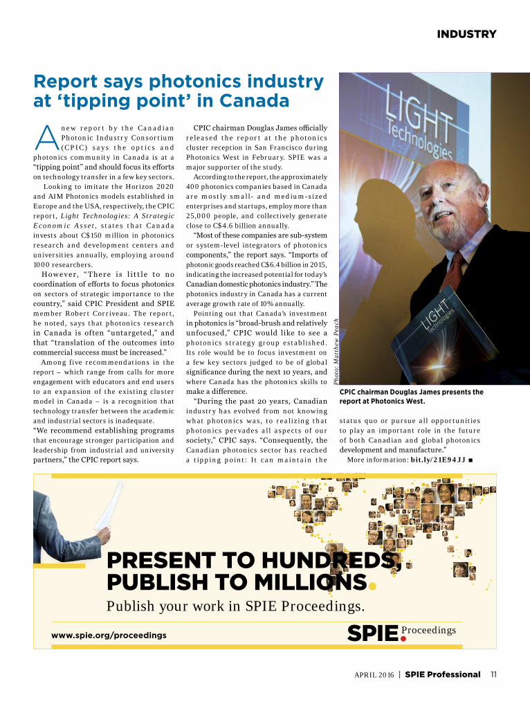
CPIC chairman Douglas James presents the report at Photonics West.
A new repor t by the Canadian Photonic Industry Consortium (C PIC ) s ay s t he opt ic s a nd
photonics community in Canada is at a “tipping point” and should focus its efforts on technology transfer in a few key sectors. Looking to imitate the Horizon 2020 and AIM Photonics models established in Europe and the USA, respectively, the CPIC report, Light Technologies: A Strategic Economic Asset, states that Canada invests about C$150 million in photonics research and development centers and universities annually, employing around 1000 researchers. How e ve r, “ T he r e i s l i t t le to no coordination of efforts to focus photonics on sectors of strategic importance to the country,” said CPIC President and SPIE member Robert Corriveau. The report, he noted, says that photonics research in Canada is of ten “untargeted,” and that “translation of the outcomes into commercial success must be increased.” Among five recommendations in the report – which range from calls for more engagement with educators and end users to an expansion of the existing cluster model in Canada – is a recognition that technology transfer between the academic and industrial sectors is inadequate. “We recommend establishing programs that encourage stronger participation and leadership from industrial and university partners,” the CPIC report says.
CPIC chairman Douglas James officially released the report at the photonics cluster reception in San Francisco during Photonics West in February. SPIE was a major supporter of the study. According to the report, the approximately 400 photonics companies based in Canada are mostly small- and medium-sized enterprises and startups, employ more than 25,000 people, and collectively generate close to C$4.6 billion annually. “Most of these companies are sub-system or system-level integrators of photonics components,” the report says. “Imports of photonic goods reached C$6.4 billion in 2015, indicating the increased potential for today’s Canadian domestic photonics industry.” The photonics industry in Canada has a current average growth rate of 10% annually. Pointing out that Canada’s investment in photonics is “broad-brush and relatively unfocused,” CPIC would like to see a photonics strategy group established. Its role would be to focus investment on a few key sectors judged to be of global significance during the next 10 years, and where Canada has the photonics skills to make a difference. “During the past 20 years, Canadian industry has evolved from not knowing what photonics was, to realizing that photonics pervades all aspects of our society,” CPIC says. “Consequently, the Canadian photonics sector has reached a t ipping point: It can maintain the
status quo or pursue all opportunities to play an important role in the future of both Canadian and global photonics development and manufacture.” More information: bit.ly/21E94JJ .
www.spie.org/proceedings Proceedings
PRESENT TO HUNDREDS, PUBLISH TO MILLIONS•Publish your work in SPIE Proceedings.
Phot
o: M
atth
ew P
each
How to joinAIM Photonics There are several ways to become a member of AIM Photonics.
The institute offers tiered membership pricing for industry, academia, and nonprofits. Each tier offers varying levels of engagement with the program, other participants, and the technology and services that are developed.
Tier 1 participants, which contribute $1 million annually to join with a five-year commitment, are expected to provide more support and will have more opportunities to work with one another and the resulting intellectual property, noted Rod Alferness, head of government and industry outreach for AIM Photonics.
Tier 2 and 3 participants, which annually contribute $500,000 and $100,000, respectively, for a three-year commitment, are more limited in their access to the program and its products and services.
Early Tier 1 academic partners include the University of Rochester, SUNY Polytechnic, RIT, MIT, Columbia, UCSB, UC Davis and University of Arizona. Early Tier 1 industry partners include Intel, HP, United Technologies, Raytheon, and Cisco.
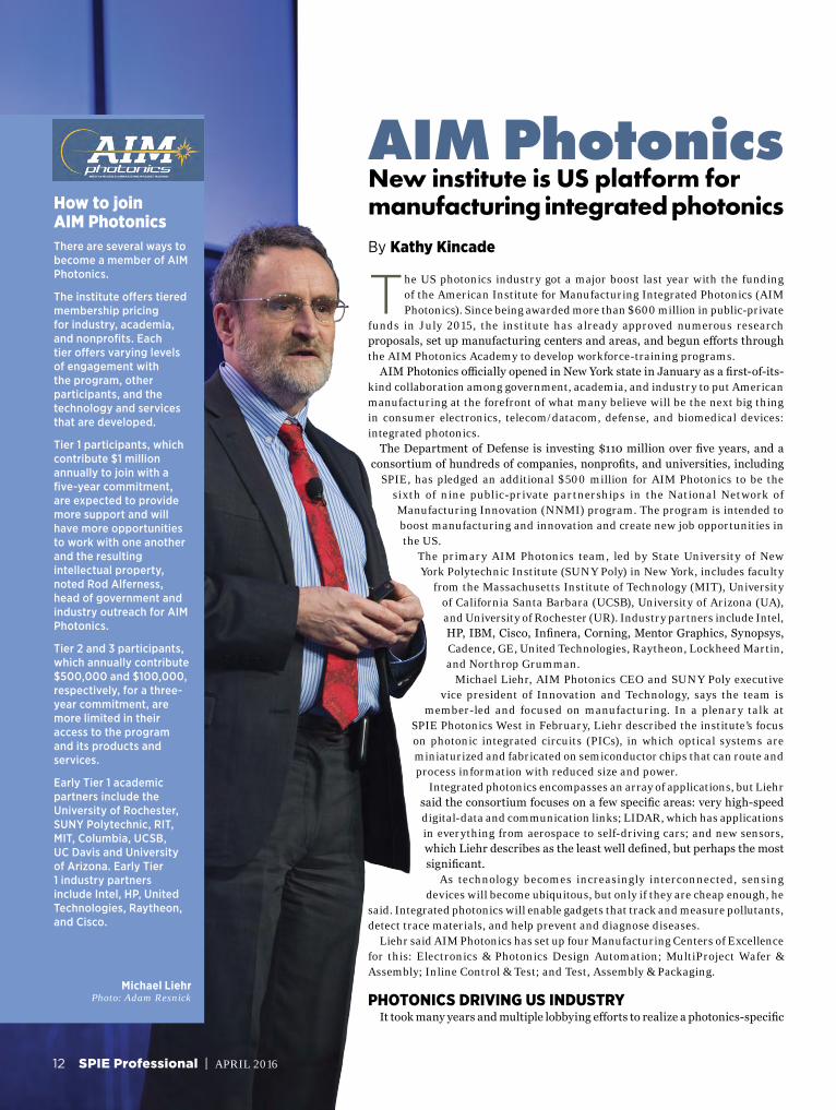
AIM PhotonicsNew institute is US platform formanufacturing integrated photonicsBy Kathy Kincade
The US photonics industry got a major boost last year with the funding of the American Institute for Manufacturing Integrated Photonics (AIM Photonics). Since being awarded more than $600 million in public-private
funds in July 2015, the institute has already approved numerous research proposals, set up manufacturing centers and areas, and begun efforts through the AIM Photonics Academy to develop workforce-training programs. AIM Photonics officially opened in New York state in January as a first-of-its-kind collaboration among government, academia, and industry to put American manufacturing at the forefront of what many believe will be the next big thing in consumer electronics, telecom/datacom, defense, and biomedical devices: integrated photonics. The Department of Defense is investing $110 million over five years, and a consortium of hundreds of companies, nonprofits, and universities, including
SPIE, has pledged an additional $500 million for AIM Photonics to be the sixth of nine public-private partnerships in the National Network of Manufacturing Innovation (NNMI) program. The program is intended to boost manufacturing and innovation and create new job opportunities in the US. The primary AIM Photonics team, led by State University of New
York Polytechnic Institute (SUNY Poly) in New York, includes faculty from the Massachusetts Institute of Technology (MIT), University
of California Santa Barbara (UCSB), University of Arizona (UA), and University of Rochester (UR). Industry partners include Intel, HP, IBM, Cisco, Infinera, Corning, Mentor Graphics, Synopsys, Cadence, GE, United Technologies, Raytheon, Lockheed Martin, and Northrop Grumman.
Michael Liehr, AIM Photonics CEO and SUNY Poly executive vice president of Innovation and Technology, says the team is
member-led and focused on manufacturing. In a plenary talk at SPIE Photonics West in February, Liehr described the institute’s focus on photonic integrated circuits (PICs), in which optical systems are miniaturized and fabricated on semiconductor chips that can route and process information with reduced size and power. Integrated photonics encompasses an array of applications, but Liehr said the consortium focuses on a few specific areas: very high-speed digital-data and communication links; LIDAR, which has applications in everything from aerospace to self-driving cars; and new sensors, which Liehr describes as the least well defined, but perhaps the most significant. As technology becomes increasingly interconnected, sensing devices will become ubiquitous, but only if they are cheap enough, he
said. Integrated photonics will enable gadgets that track and measure pollutants, detect trace materials, and help prevent and diagnose diseases. Liehr said AIM Photonics has set up four Manufacturing Centers of Excellence for this: Electronics & Photonics Design Automation; MultiProject Wafer & Assembly; Inline Control & Test; and Test, Assembly & Packaging.
PHOTONICS DRIVING US INDUSTRY It took many years and multiple lobbying efforts to realize a photonics-specific
Michael Liehr Photo: Adam Resnick
12 SPIE Professional | APRIL 2016
SPIE membersadvocatefor the NPI The US National Photonics Initiative (NPI) is a collaborative alliance among industry, academia, and government to raise awareness of photonics and the impact of photonics on our everyday lives.
By increasing cooperation and coordination among these groups, the NPI advances photonics-driven fields and strives to drive US funding and investment in photonics in order to maintain US economic competitiveness and national security.
SPIE is a founding sponsor of the NPI and is leading the initiative along with the American Physical Society (APS), IEEE Photonics Society, Laser Institute of America (LIA), and the Optical Society (OSA).
For more information, visit spie.org/NPI.
NNMI in America. A key turning point came in August 2012 when the National Research Council (NRC) of the National Academies released its report “Optics and Photonics, Essential Technologies for Our Nation.” That report assessed the current state of optics, photonics, and optical engineering in the US, prioritized research grand-challenge questions to fill technological gaps, and recommended actions to support global leadership in photonics-driven industry. It also led to the creation of the National Photonics Initiative (NPI) to raise general awareness of photonics and its role in our everyday lives; increase coordination among industry, government, and academia; and drive US funding and investment. SPI E i s a fou nd i ng sponsor of the NPI. “It is a good t ime to make this k ind of investment,” said Tom Koch, dean of the College of Optical Sciences at UA and chair of AIM Photonics’ Technical Review Board. “Some really interesting advances in optics and photonics technologies have emerged in recent years, and they are continuing to leverage more and more the huge investments that go into microelectronics manufacturing.” Too often the breakthrough research at US universities ends up getting made outside the US, says John Bowers, professor of electrical and computer engineering and materials at UCSB, which is overseeing the West Coast hub of AIM Photonics. “So that’s what the NPI and AIM Photonics are trying to fix. We want to use American ingenuity and inventions to benefit American industry.”
WHY INTEGRATED PHOTONICS? The decision to focus on PICs also had its roots in the 2012 NRC report. “In that report, one of the top f ive bullets was integrated photonics,” said Rod Alferness, dean of UCSB’s College of Engineering and head of government and industry outreach for AIM Photonics. “We realized the ability to integrate together multiple functions and devices to get larger functionality was going to be critical to the continued advancement and application of optics in a number of areas. We also believed it would be critically important to provide the interconnect technologies inside of large data centers, and that large data centers would be at the heart of economic growth.” Integrated photonics is “an unbelievable game changer,” said Tom Battley, executive director of the Rochester Regional Photonics Cluster and New York Photonics, a key player in the efforts that helped make AIM Photonics a reality. “It’s like going from
buggy whips to motorized cars. It’s going to radically transform our lives, without question.”
A PIC FOUNDRY INFRASTRUCTURE The integrated photonics foundry infrastructure is immature in the USA, and establishing a strong one will enable broader access to PIC technology and design and manufacturing resources for companies of all sizes, Liehr notes. “The idea is to build something that is modeled after the Fraunhofer program in Germany, which is serving the local German economy by providing a path, especially for smaller companies, that have a demand for, say, very small production runs
for research that they couldn’t afford because they can’t af ford the infrastructure,” he said. Each AIM Photonics partner brings its own unique expertise to the effort. SUNY Poly, for example, is well known f o r i t s f a b r i c a t i o n capabilities, while MIT
and UCSB are national R&D leaders in silicon photonics and integrating lasers into silicon. Rochester Institute of Technology (RIT), UR, UA, and Columbia University will contribute packaging, assembly, and test solutions for PICs, while all partners will pursue applications advances. On the industry side, Intel and HP both have very advanced photonics platforms, Bowers noted, while Infinera has developed some of the most complex PICs currently available. “The role of photonics in so many aspects of our lives has become increasingly difficult to ignore when you begin to realize how dependent we are on the Internet, our smart phones, displays, … so many things that are optical,” Koch said. In Arizona, “we’re now getting engaged by all the IT companies because they all realize that the human interface into smart systems involves a lot of optics. We even signed a deal with Uber because they realize that their cars, interfacing with the world, require a lot of optics.” The AIM Photonics team is already looking at ways to address the design, packaging, and assembly cha l lenges that must be resolved before PIC technology is ready for broad-based commercialization and volume manufacturing. AIM Photonics believes its collaborative approach is just what the industry needs at this point. The goal is to put in place an end-to-end photonics “ecosystem:” domestic foundry access; integrated design tools; automated packaging, assembly and testing; workforce development; and a standardized
SPIEDigitalLibrary.org
Find the Answer
Energy
“Our goal is to integrate everything together onto a chip and to manufacture them in high volume. If we can do that, we end up with far cheaper packaging and far fewer interfaces.”
–John Bowers, AIM Photonics’ West Coast hub
INDUSTRY
Continued on page 14
13APRIL 2016 | SPIE Professional
14 SPIE Professional | APRIL 2016
AIM PHOTONICSt Continued from page 13
platform to make it easier to scale the technology across multiple markets for companies of all sizes. “If you look at the model for AIM Photonics, it is really about building a complete ecosystem for this industry,” Alferness said. “It’s about leveraging federal dollars to do that, but also leveraging cost-share dollars from companies that will become members of the institute in order to share technology and build up this ecosystem. “The more companies we have with a broad set of skills and capabilities, the more powerful the institute will become and the better the value proposition. We believe that is especially true for the small- to medium-sized enterprises. The ecosystem becomes complete because they have the opportunity to make integrated photonics devices without having to invest in all the infrastructure,” he said.
WORKFORCE DEVELOPMENT SPIE member Lionel Kimerling, the MIT professor in charge of education and workforce development for AIM Photonics, says the AIM Photonics Academy will provide a unified learning, training, knowledge, technology, and workforce deployment platform. The goal is to attract and retain community college, undergraduate, graduate students, and veterans and help them prepare for careers in the photonics industry. Through the academy, these students will have access to internships, apprenticeships and classes on photonic system modeling; design automation; materials and processing, metrology and testing, integrated photonics packaging and integrated photonics applications. For example, Columbia University hosted a weeklong PIC training workshop in October 2015 that introduced attendees to the critical aspects of producing integrated optical components. “There is a substantial effort going into this,” Alferness said. “At UCSB, we have an organization that has focused on outreach in general in helping to make sure we are training people in technology areas, starting in high school.
“If you look at what will be the products coming out of AIM Photonics, part of how we will keep products in the US is that instead of using low-cost labor to put devices together and build modules, we are focusing on integrated devices using technology that will require advanced, bachelor, and associates degrees with technical capability. “The result will be more high-paying and education-based jobs in lieu of what we typically think of as assembly line jobs,” he said.
SELF-SUSTAINING PRIORITY One priority project area for AIM Photonics involves using complementary metal-oxide semiconductor (CMOS) processing to move photonics onto silicon to eliminate the data bottleneck that advanced silicon chips are facing during the next decade. Thus, high-port-count switches is one of the institute’s first projects. Another area of interest is 3D stacking of electronics with optics. “The ability to co-manufacture these as a single-chip subassembly on a wafer scale rather than chip by chip. This is an example of one of the most game-changing capabilities of PICs,” Koch said. “It will take a few years to see it emerge in commercial solutions. But when it does, it will be very powerful.” The real test of success will be whether AIM Photonics can become self-sustaining and what kind of commercial value it can bring to its members in the process, Koch emphasized. “The big milestone for us is we know we need to be self-sufficient in five years, and the only way you do that is by bringing value,” he said. For details about AIM Photonics, including its structure, projects, goals, and membership requirements, go to aimPhotonics.com. To s e e s l ide s f r om a Novemb er 201 5 webi n a r, v i s i t bit.ly/1PlBNk4. .–Kathy Kincade is a freelance science and technology writer based in California (USA)
INDUSTRY
International students get US employment reprieve
The US Department of Homeland Security has updated a rule allowing some international students to work in the United States for up to 36 months following graduation.
The students in select science, technology, engineering and math (STEM) fields had been under a cloud of uncertainty after a
court ruled that a 2008 regulation had not gone through the official rule-making process. The Obama administration was ordered to establish a formal rule extending the previous period for graduate STEM workers by nine months. The new rule takes effect 10 May. The Optional Practical Training (OPT) program allows international students an initial period of 12 months of employment, followed by the additional 24 months afforded by the new rule.
“This is such an important issue because it is very difficult to find a job placement within the current 12-month post-graduation time frame,” said Naman Mehta, a master’s degree student from India and vice president of the SPIE Student Chapter at CREOL, University of Central Florida. Mehta will graduate this spring and is preparing his CV to begin his job search, he said. “Extending the time frame to 36 months would allow international students to better contribute to American innovation industries and institutions. And why is this bad?” he asked. “Why incentivize these students to find employment elsewhere?” The new rule requires international students and employers to develop individualized training plans that enhance students’ educational experience with practical training. It also allows for two lifetime OPT extensions instead of one and provides eligibility for non-STEM graduates to participate if they obtained a STEM degree in the past 10 years at an accredited college or university. DHS estimates that about 34,000 individuals are currently participating in this program and that the total number of affected students will expand in the coming years. .SPIEDigitalLibrary.org
Find the Answer
Lasers

After what is described as a “momentous” 2015 for solar power in the US, this year will smash all previous records, with installations set to more than double, according to Greentech
Media Research. The Greentech analyst team predicts that close to 16 GW of photovoltaic power will be installed this year – up from the record figure of 7.3 GW in 2015. Dozens of major utility buildouts are already in the pipeline ahead of what had previously been expected to be the final year in which projects could qualify for the US investment tax credit (ITC). In the executive summary of their US Solar Market Insight report, lead author Cory Honeyman and colleagues at GTM Research and the Solar Energy Industries Association write that 2015 was “a historic year for US solar policy and regulation, with a number of decisions at both the state and federal level that will determine the trajectory of the market’s future growth.” With an extension of the ITC approved through at least 2021, GTM Research now estimates an increase in more than 50% net growth in
US solar installations between 2016 and 2020. That’s an additional 24 GW compared with what had previously been expected. “As a result of this change and other market developments since December, we now anticipate that cumulative solar photovoltaic installations will reach 97 GW by the end of 2020,” the analyst team added. The report also confirms earlier suggestions that more PV power was added to the US grid in 2015 than any other form of electricity-generating capacity except wind. PV accounted for 29.4% of the new generating capacity, with natural gas responsible for 29% and wind power 39%. In stark contrast, the prospects for both forms of concentrating solar power, thermal (CSP) and PV (CPV), are “bleak,” the analysts say. The outlook for CPV is looking particularly bad, with a recent report from the US National Renewable Energy Lab and Fraunhofer Institute for Solar Energy Systems describing the industry as being “in severe crisis.” .
US solar market set to double in size
15APRIL 2016 | SPIE Professional
INDUSTRY
FRED® – Photon Engineering’s leading optical engineering software – works seamlessly with your optical design and CAD
software to achieve your final results quickly and accurately.
Find out why major universities, national labs, and government and
aerospace organizations around the world depend on FRED to play
an integral role in their scientific and engineering projects.
There’s never been a better time to add FRED® software to the equation.
Get the right result when FRED software is part of the equation.
Coherent beam propagation
Stray light analysis
Illumination and non-imagingoptical design
Imaging system analysis
Multi-wavelength characterization
Thermal imagery
520.733.9557 | 310 S. Williams Blvd., Suite 222 | Tucson, AZ 85711 www.photonengr.com

16 SPIE Professional | APRIL 2016
CONTRIBUTETO A BETTERWORLDOptical and photonics technologies — and the people who work with them — have brought tangible social, environmental, health, and economic gains to humanity.
Whether by bringing inexpensive and efficient alternative energy to rural and developing areas, ensuring the safety of our food, or enabling instant communications, researchers, educators, and industry professionals have advanced light-based research and technologies for the betterment of the human condition.
Do you have a story to contribute or a question about how optics and photonics technologies benefit humanity?
Write to us at [email protected].
Read more articles and blog posts celebrating the many ways that optics and photonics are applied in creating a better world at PhotonicsForaBetter World.org.
Photonics for a Better World
GAMING TECHNOLOGY MAY ENABLE BETTER ASSESSMENTS OF MS PATIENTS
PHOTONICS FOR A BETTER WORLD
Microsoft and global healthcare company Novartis have joined forces against multiple sclerosis (MS), a disabling disease that
affects the immune and central nervous systems of millions of people worldwide. A new tool called Assess MS, to be tested soon in clinical trials, uses Microsoft’s Kinect gaming system to monitor and evaluate a patient’s movements to determine if the disease is progressing or not. Assessing whether a patient’s symptoms are stabilizing or getting worse is complicated, and Novartis and other healthcare companies have been searching for years for a consistent way to quantify whether treatments being developed for MS are working. With MS, sy mptoms might progress w ith heartbreaking speed while in others they may show up slowly, erratically, and over a period of many years.“One of the most difficult things about MS is the uncertainty of it,” said Cecily Morrison, a researcher working on the project in Microsoft’s Cambridge (UK) research lab. In standard tests to quantify the progress of multiple sclerosis, doctors typically ask patients to touch their nose or sit with their arms outstretched. Doctors watch the patients and then use a rating scale to determine how strong the patients’ symptoms are. The problem? Doctors are only human, and despite all their best efforts to standardize the MS test, in the end it is subjective. The researchers found that when a group of doctors are shown the same patient doing the same movement, some may interpret it as a “1” on the rating scale, while others will say it’s a “2.” Even when the same doctor is shown the same movement on two different days, that doctor may give that patient a different rating. “The clinicians that we worked with really care about their patients. They really want what’s best for them, and even the best neurologist will admit that when they use these rating scales, it’s pretty coarse-grained,” said Abigail Sellen, a principal researcher in Microsoft’s Human Experience and Design group in Cambridge. “They know that there’s a lot of variability, even in their own judgments, over time.”
MACHINE LEARNING TECHNOLOGY When Microsoft released the Kinect system for playing Xbox video games about five years ago, researchers at Novartis thought the computer vision and machine learning technology inside the Kinect
might help doctors get a more consistent reading of how a patient performed on each of the tests. A uniform measurement of MS systems could also speed up the process of getting the right treatments to patients. Microsoft researchers agreed to Novartis’ idea, knowing that machine learning would be ideal for a project like Assess MS because, as the computer vision system captures more recordings of patient movements, it can deliver more consistent results showing the disease’s progression. “It was clear that this was a very ambitious project,” said Peter Kontschieder, a postdoctoral researcher at Microsoft who has built many of the machine learning algorithms used in the Assess MS project. In a typical machine learning scenario, an experiment starts with a huge amount of data, such as many pictures of trees. The computer is given those pictures and, using a machine learning algorithm, it creates a model that recognizes what a tree looks like. Then, the next time it sees a picture of a tree — even if it wasn’t one of the pictures it was originally shown — it has learned to identify the image as a tree.
GATHERING DATA A CHALLENGE For the Assess MS project, the first challenge was gathering data. In order to get an accurate view of how an MS patient was faring, researchers needed to figure out a way to make the Kinect depth camera, which is designed to recognize the sweeping gestures of playing a living-room video game, pick up on subtle movements such as the sway of a patient’s torso. That required the researchers to come up with entirely new algorithms that would work behind the scenes with the Kinect’s depth camera and that would both recognize the patients’ body parts in a more nuanced way and provide a more precise representation of how the patient was doing on each of the tests. Even once they had created those algorithms from scratch, the machine learning experts still knew they wouldn’t be able to collect as much data as they would ideally want to have to create a machine learning model. That’s because they were gathering these types of recordings for the first time, and they would be limited in how they could use the data by stringent patient privacy protections. There was a third challenge as well. Unlike simple

17APRIL 2016 | SPIE Professional
SPIEDigitalLibrary.org
Find the Answer
Optics & Astronomy
TECHNOLOGY R&D
RECOMMENDED READING
The chain that binds usBy Eddie L. Jacobs
Has the imaging chain become the old ball and chain? Does your love of the image-formation process need a little something to rekindle
the spark? Instead of searching the self-help section on Amazon, might I suggest you take a look at the article “Radiance and photon noise: imaging in geometrical optics, physical optics, quantum optics and radiology” by Luca Caucci, SPIE Fellow Kyle J. Myers, and SPIE member Harrison Barrett in the January issue of Optical Engineering. The article appears in a special section on techniques for structural health monitoring. Coming from medical imaging backgrounds, the authors examine the imaging chain from several perspectives. They develop the radiance concept in geometrical, physical, and quantum optical domains and the governing conservation laws. They then examine the fundamental relationship between radiance and noise in imaging systems for integrating, photon counting, and photon-processing detector types. Photon-processing detectors and the concepts related to them are increasingly being employed in light-field cameras and other advanced imaging systems. The authors conclude with a discussion of the information content of a photon and image quality as they relate to radiance and noise. Barrett, who received the 2011 SPIE Gold Medal
for a lifetime of contributions to imaging science, and Caucci are on the faculty at University of Arizona (USA). Myers, a UA graduate who works at the US Food and Drug Administration, and Barrett, were the first recipients of the Joseph W. Goodman Book Writing Award for their 2003 book, Foundations of Image Science (John Wiley & Sons, 2003). I found this article gave me some new insight into the image formation process and some great ideas to pursue in my lab. Taking a fresh look at the imaging chain was a great way to begin a new year of optical engineering. Give it a read! S o u r c e h t t p ://d x . d o i . o r g /10 .1 1 17/1 .OE.55.1.013102 .– SPIE Fellow Eddie L. Jacobs of University of Memphis is a member of the Optical Engineering editorial board.
image recognition, in which you can say one picture is a tree and another is a car, this project required the researchers to grapple with nuanced, subjective data showing even slight disease progression. All of these challenges required new strategies for labeling data consistently, so that they could create a strong model for quantifying the results accurately. Another element of the project involved designing the system to fit into a real exam room, which might be small or crowded or have things like chairs in the way. It also had to be easy for doctors and nurses to operate. After years of working on design and algorithms, the researchers say they have developed a proof of
concept, using a limited number of patients, so they know the system works in principle. The next step is to test Assess MS in practice, so they can see how it works with a larger number of patients. Ultimately, the researchers hope Novartis and other pharmaceutical companies can use Assess MS to speed up clinical trials for treatments of multiple sclerosis, and perhaps, eventually, for other, similar diseases as well. “Novartis is leveraging digital technologies to transform patient care and drug development,” said Vas Narasimhan, a Harvard-trained physician who is now global head of development at Novartis Pharmaceuticals. .
Diagram shows that radiance in a homogeneous medium is a line integral of a volumetric source that does not absorb or scatter its own radiation. The cross indicates the origin of coordinates for the three 3D position vectors.
Source
R2
s
ss
R3R1

18 SPIE Professional | APRIL 2016
Daily news fromPhotonics WestThe Photonics West Show Daily was distributed in San Francisco, CA (USA) each day of the Photonics West exhibition in February.
The newspapers are available as PDFs at optics.org/ShowDaily
More highlights from Photonics West can be found on page 24 and at spie.org/PWnews Hot technical topics at SPIE Photonics West
in February included neurophotonics, 3D printing and imaging, miniaturization
in biomedical devices as well as sensors and optoelectronic devices, photoacoustic sensing, fiber lasers, and silicon photonics. The annual LASE, OPTO, and BiOS conferences, with more than 4800 technical presentations and 67 courses and workshops, provided an international forum for researchers to report and discuss their latest results with peers, collaborators, and the business community. A record number of registrations exceeded 22,000, and there was a record number of exhibiting companies in the Photonics West Exhibition (1,345) in San Francisco, CA (USA), as well. The separate weekend BiOS Expo included 212 companies. The growing participation ref lected research-funding and market opportunity for photonics and the strength of the photonics industry overall. An extensive industry and professional development program complemented the technical conferences, with panels and workshops on 3D printing, silicon photonics, intellectual property, marketing, export rules, and business perspectives from industry executives. The weeklong event also included a two-day job fair, the SPIE Startup Challenge (see page 6), and the Prism Awards for Photonics Innovation, honoring the most promising new products launched in 2015 (see page 4). In an update on the ongoing SPIE analysis of the global photonics market, Stephen G. Anderson, SPIE director of industry development, reviewed the growing markets enabled by optics and photonics products. Total application revenues are approaching USD$1.5 trillion, and the greater industry employs more than 3.5 million people, the SPIE study shows. Panelists discussing 3D printing explored not only the technicalities of the field, but intellectual property challenges, cybersecurity threats, and ethical issues. The technology makes possible the production of lightweight airplane and automobile parts with 3D printers and has the potential to produce human tissue.
“SPIE Photonics West is firmly established as the must-attend event in our industry,” said Andrew Brown, SPIE senior director for global business development. “Photonics is the future, and this is where the world’s innovators and business leaders gather every year to launch new products, find new markets, and drive this industry forward.” A sampling of the highlights are below and online at spie.org/PWnews. See page 24 for more on BiOS.
BRAIN INITIATIVE Research on the workings of the brain was advanced in a new program track on neurophotonics organized by Rafael Yuste of Columbia University, who helped conceptualize and launch the US Brain Research through Advancing Innovative Neurotechnologies (BRAIN) initiative. In addition, a neuroscience task force of the US National Photonics Initiative hosted a “hot topics” session on the BRAIN initiative. More than 150 people attended a Sunday afternoon discussion and networking reception that featured speakers from federal agencies, academia, and industry who described progress in mapping brain function, work which is enabled by several photonics technologies and applications, such as sensors, lasers, and imaging devices. Ned Talley, a program director with the National Institutes of Health (NIH), illustrated the need for better understanding of disorders of the brain by pointing out that they have become the most costly of chronic diseases in the US, even more than cancer and cardiovascular disease. “We don’t know enough about the brain to meet this challenge,” he said. Even so, he said, “the tools we have, including photonics tools, are starting to look extremely promising.” As part of the BRAIN initiative, the NIH has developed a formal program for public-private partnerships, Talley said. Last year, the agency spent $85 million to support 125 projects, he said, and so far, the initiative is receiving strong bipartisan support in Congress for funding. The photonics industry has a huge role to play in
PHOTONICS WEST BREAKSNEW PARTICIPATION RECORDS
SPIEDigitalLibrary.org
Find the Answer
Optoelectronics & Communications
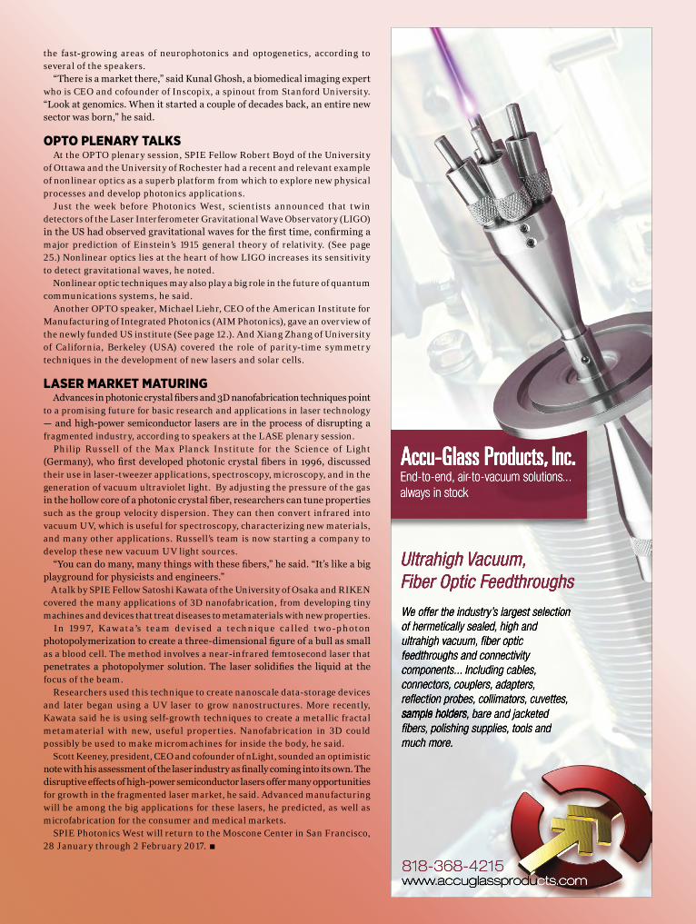
19APRIL 2016 | SPIE Professional818-368-4215www.accuglassproducts.com
Accu-Glass Products, Inc.End-to-end, air-to-vacuum solutions...always in stock
Ultrahigh Vacuum,Fiber Optic FeedthroughsWe offer the industry’s largest selection of hermetically sealed, high and ultrahigh vacuum, fiber optic feedthroughs and connectivity components... Including cables, connectors, couplers, adapters, reflection probes, collimators, cuvettes, sample holderssample holders, bare and jacketed fibers, polishing supplies, tools and much more.
the fast-growing areas of neurophotonics and optogenetics, according to several of the speakers. “There is a market there,” said Kunal Ghosh, a biomedical imaging expert who is CEO and cofounder of Inscopix, a spinout from Stanford University. “Look at genomics. When it started a couple of decades back, an entire new sector was born,” he said.
OPTO PLENARY TALKS At the OPTO plenary session, SPIE Fellow Robert Boyd of the University of Ottawa and the University of Rochester had a recent and relevant example of nonlinear optics as a superb platform from which to explore new physical processes and develop photonics applications. Just the week before Photonics West, scientists announced that twin detectors of the Laser Interferometer Gravitational Wave Observatory (LIGO) in the US had observed gravitational waves for the first time, confirming a major prediction of Einstein’s 1915 general theory of relativity. (See page 25.) Nonlinear optics lies at the heart of how LIGO increases its sensitivity to detect gravitational waves, he noted. Nonlinear optic techniques may also play a big role in the future of quantum communications systems, he said. Another OPTO speaker, Michael Liehr, CEO of the American Institute for Manufacturing of Integrated Photonics (AIM Photonics), gave an overview of the newly funded US institute (See page 12.). And Xiang Zhang of University of California, Berkeley (USA) covered the role of parity-time symmetry techniques in the development of new lasers and solar cells.
LASER MARKET MATURING Advances in photonic crystal fibers and 3D nanofabrication techniques point to a promising future for basic research and applications in laser technology — and high-power semiconductor lasers are in the process of disrupting a fragmented industry, according to speakers at the LASE plenary session. Philip Russell of the Max Planck Institute for the Science of Light (Germany), who first developed photonic crystal fibers in 1996, discussed their use in laser-tweezer applications, spectroscopy, microscopy, and in the generation of vacuum ultraviolet light. By adjusting the pressure of the gas in the hollow core of a photonic crystal fiber, researchers can tune properties such as the group velocity dispersion. They can then convert infrared into vacuum UV, which is useful for spectroscopy, characterizing new materials, and many other applications. Russell’s team is now starting a company to develop these new vacuum UV light sources. “You can do many, many things with these fibers,” he said. “It’s like a big playground for physicists and engineers.” A talk by SPIE Fellow Satoshi Kawata of the University of Osaka and RIKEN covered the many applications of 3D nanofabrication, from developing tiny machines and devices that treat diseases to metamaterials with new properties. In 1997, Kawata’s team devised a technique called two-photon photopolymerization to create a three-dimensional figure of a bull as small as a blood cell. The method involves a near-infrared femtosecond laser that penetrates a photopolymer solution. The laser solidifies the liquid at the focus of the beam. Researchers used this technique to create nanoscale data-storage devices and later began using a UV laser to grow nanostructures. More recently, Kawata said he is using self-growth techniques to create a metallic fractal metamaterial with new, useful properties. Nanofabrication in 3D could possibly be used to make micromachines for inside the body, he said. Scott Keeney, president, CEO and cofounder of nLight, sounded an optimistic note with his assessment of the laser industry as finally coming into its own. The disruptive effects of high-power semiconductor lasers offer many opportunities for growth in the fragmented laser market, he said. Advanced manufacturing will be among the big applications for these lasers, he predicted, as well as microfabrication for the consumer and medical markets. SPIE Photonics West will return to the Moscone Center in San Francisco, 28 January through 2 February 2017. .

TECHNOLOGY R&D
Thousands of photomultiplier tubes observe neutrino oscillation in Nobel Prize-winning experiments
By Chris Warner
PHOTOMULTIPLIERS SCAN THE UNIVERSE Thirteen years after Koshiba’s Nobel honor, Takaaki Kajita and Arthur B. McDonald received the 2015 Nobel Prize in Physics for neutrino-related research. Kajita’s work took place at Kamiokande and later at its successor, Super-Kamiokande (Super-K). In 1998, Kajita’s team observed that muon neutrinos, one of three types, or “flavors,” of neutrinos (muon, tau, and electron) from cosmic rays would disappear before reaching the Kamiokande detector. The scientists observed that the muon neutrinos became tau neutrinos as they passed through Earth. According to quantum theory, particles that transform themselves in this way — “oscillation” — must carry some mass. This proof of neutrino oscillation challenges widely held beliefs about subatomic particles because the Standard Model of particle physics considers neutrinos to have a mass of zero. The neutrino oscillations were detected by photomultiplier tubes (PMTs), versatile photodetection devices that can quietly scan the universe for single-photoelectron-level clues. Both Kamiokande and Super-K use thousands of 20-inch PMTs to collect very weak light signals, convert them to photoelectrons, and then amplify them so external circuitry can detect them. Twenty-inch PMTs were unheard of when Koshiba asked Hamamatsu Photonics to develop them for use in Kamiokande. It took years of development, factory modifications, and process enhancements to fulfill the ambitious order. When delivered, this was the pinnacle of engineering for a device that has been around since the 1930s.
DETECT NEUTRINOS CHANGING IDENTITIES
20 SPIE Professional | APRIL 2016
Supernova explosions are believed to occur once every few centuries. One such event was seen with the naked eye in 1604, and the next observation happened in February
1987 inside a gigantic physics laboratory at Kamioka, Japan, one kilometer under the bedrock of Mount Ikeno. Kamiokande, the University of Tokyo’s Kamioka Nucleon Decay Experiment, detected neutrinos from supernova 1987A emanating from the Large Magellanic Cloud some 160,000 light years from Earth. These sub-atomic particles rarely interact with other matter, making them very difficult to detect. In a span of a few seconds, Kamiokande detected 11 out of the estimated 2 x 1058 neutrinos released by the supernova. Although the sample size was miniscule in relation to the enormous number of neutrinos that bombarded Earth from the 1987A, it was remarkable because it was the first time neutrinos from a supernova had been observed. This very rare event led to a share of the 2002 Nobel Prize in Physics for Masatoshi Koshiba, a professor at the University of Tokyo, and it ushered in the era of neutrino astronomy.
PHOTOMULTIPLIER TUBES

TECHNOLOGY R&D
Today, PMTs are indispensable for neutrino research and other modern-day applications.
PMTS AND PROTON DECAY EXPERIMENTS When light strikes the glass of a PMT, it excites electrons in a thin-film photoelectric surface (photocathode) on the inner side of the glass bulb. The electrons are then emitted as photoelectrons into the vacuum tube. A focusing electrode collects the photoelectrons for a secondary electron multiplier made of a series of dynodes (stages). The electric field of the first dynode accelerates the electrons and releases secondary electrons. The process continues for 10 stages or more until there is a sufficient signal to be collected by an anode as a large output current. The ratio of the anode’s output current to the photoelectric current from the photocathode is its current amplification, or “gain.” Koshiba originally conceived the observatory to study proton decay through Cherenkov radiation experiments. Cherenkov radiation occurs because, in a transparent medium such as water, proton decay or neutrino interactions produce secondary charged particles that sometimes fly outward faster than the speed of light, thus creating a blue flash with a wavelength in the 350nm to 400nm range. Converting the very weak Cherenkov radiation emissions to electric signals requires the light to be amplified 10 million times. To provide such a high gain and a very wide field of view, the 20-inch PMTs were given 75-mm x 75-mm dynodes arranged in a “venetian blind” configuration.
AMBITIOUS REQUIREMENTS Water-Cherenkov radiation experiments require a large-scale observatory. In the case of Kamiokande,
a tank was filled with 3000 tons of pure water and positioned deep underground to filter out cosmic rays. So Koshiba asked for not only a large detector, but lots of them. The largest PMT prototypes at the time had a diameter of eight inches, so Hamamatsu Photonics faced a formidable challenge in developing the 20-inch PMTs, which were necessary both to capture as much of the proton decay process as possible and keep signal-processing circuits to a minimum. The PMTs’ timing was another highly critical specification for Koshiba. Cherenkov light is only emitted in the direction of the elementary particle’s movement, so a PMT needs fast timing response to
21APRIL 2016 | SPIE Professional
A 20-inch-diameter photomultiplier tube (PMT) for water-Cherenkov observatories such as Super- Kamiokande.
Continued on page 22
Nobel Prizes,neurophotonics,and the NPIThe US National Photonics Initiative (NPI), an alliance of scientific societies uniting industry and academia to raise awareness of photonics, congratulated Takaaki Kajita, winner of the 2015 Nobel Prize in Physics, and NPI Photonics Industry Neuroscience Group member Hamamatsu Photonics (Japan) on the technology it contributed to Kajita’s Nobel Prize-winning research.
Kajita conducted his research at the Super-Kamiokande neutrino detector facility at the University of Tokyo with photomultiplier tubes (PMTs) supplied by Hamamatsu Photonics. PMTs, one of Hamamatsu’s core products, are essential components in a wide variety of scientific, commercial, and medical instruments.
“This win is a tremendous accomplishment for Kajita and Hamamatsu Photonics,” said NPI Photonics Industry Neuroscience Group Chairman Tom Baer, noting that the company has played a part in past Nobel-Prize-winning research as well.
The awarding of the Nobel Prize is also important to the optics and photonics community because “it underscores the key role of optics and photonics in scientific discoveries that advance our basic understanding of the world in which we live,” he said.
The NPI Photonics Industry Neuroscience Group has committed more than $30 million in existing and future R&D spending over the next three years to advance optics and photonics technology in support of the White House Brain Research through Advancing Imaging Neurotechnologies (BRAIN) Initiative.
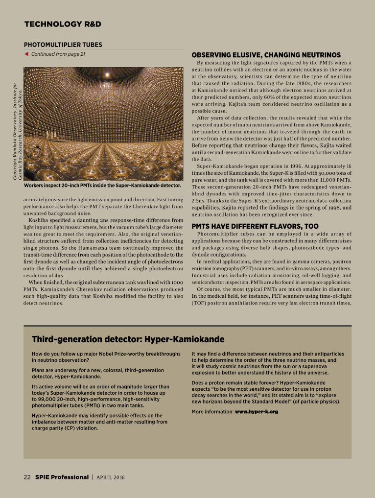
22 SPIE Professional | APRIL 2016
TECHNOLOGY R&D
PHOTOMULTIPLIER TUBESt Continued from page 21
accurately measure the light emission point and direction. Fast timing performance also helps the PMT separate the Cherenkov light from unwanted background noise. Koshiba specified a daunting 2ns response-time difference from light input to light measurement, but the vacuum tube’s large diameter was too great to meet the requirement. Also, the original venetian-blind structure suffered from collection inefficiencies for detecting single photons. So the Hamamatsu team continually improved the transit-time difference from each position of the photocathode to the first dynode as well as changed the incident angle of photoelectrons onto the first dynode until they achieved a single photoelectron resolution of 4ns. When finished, the original subterranean tank was lined with 1000 PMTs. Kamiokande’s Cherenkov radiation observations produced such high-quality data that Koshiba modified the facility to also detect neutrinos.
OBSERVING ELUSIVE, CHANGING NEUTRINOS By measuring the light signatures captured by the PMTs when a neutrino collides with an electron or an atomic nucleus in the water at the observatory, scientists can determine the type of neutrino that caused the radiation. During the late 1980s, the researchers at Kamiokande noticed that although electron neutrinos arrived at their predicted numbers, only 60% of the expected muon neutrinos were arriving. Kajita’s team considered neutrino oscillation as a possible cause. After years of data collection, the results revealed that while the expected number of muon neutrinos arrived from above Kamiokande, the number of muon neutrinos that traveled through the earth to arrive from below the detector was just half of the predicted number. Before reporting that neutrinos change their flavors, Kajita waited until a second-generation Kamiokande went online to further validate the data. Super-Kamiokande began operation in 1996. At approximately 16 times the size of Kamiokande, the Super-K is filled with 50,000 tons of pure water, and the tank wall is covered with more than 11,000 PMTs.These second-generation 20-inch PMTs have redesigned venetian-blind dynodes with improved time-jitter characteristics down to 2.5ns. Thanks to the Super-K’s extraordinary neutrino data-collection capabilities, Kajita reported the findings in the spring of 1998, and neutrino oscillation has been recognized ever since.
PMTS HAVE DIFFERENT FLAVORS, TOO Photomultiplier tubes can be employed in a wide array of applications because they can be constructed in many different sizes and packages using diverse bulb shapes, photocathode types, and dynode configurations. In medical applications, they are found in gamma cameras, positron emission tomography (PET) scanners, and in-vitro assays, among others. Industrial uses include radiation monitoring, oil-well logging, and semiconductor inspection. PMTs are also found in aerospace applications. Of course, the most typical PMTs are much smaller in diameter. In the medical field, for instance, PET scanners using time-of-flight (TOF) positron annihilation require very fast electron transit times,
Workers inspect 20-inch PMTs inside the Super-Kamiokande detector.
Copy
righ
t Kam
ioka
Obs
erva
tory
, Ins
titu
te fo
r Co
smic
Ray
Res
earc
h, U
nive
rsit
y of
Tok
yo.
Third-generation detector: Hyper-KamiokandeIt may find a difference between neutrinos and their antiparticles to help determine the order of the three neutrino masses, and it will study cosmic neutrinos from the sun or a supernova explosion to better understand the history of the universe.
Does a proton remain stable forever? Hyper-Kamiokande expects “to be the most sensitive detector for use in proton decay searches in the world,” and its stated aim is to “explore new horizons beyond the Standard Model” (of particle physics).
More information: www.hyper-k.org
How do you follow up major Nobel Prize-worthy breakthroughs in neutrino observation?
Plans are underway for a new, colossal, third-generation detector, Hyper-Kamiokande.
Its active volume will be an order of magnitude larger than today’s Super-Kamiokande detector in order to house up to 99,000 20-inch, high-performance, high-sensitivity photomultiplier tubes (PMTs) in two main tanks.
Hyper-Kamiokande may identify possible effects on the imbalance between matter and anti-matter resulting from charge parity (CP) violation.

23APRIL 2016 | SPIE Professional
TECHNOLOGY R&D
so PMT bulb diameters are typically only one inch or more with a linear-focused arrangement of much smaller dynodes. For extremely tight spaces, Micro PMTs measure just a few millimeters in size, and they are at the forefront of the trend toward handheld medical and industrial instruments. A n o t h e r h i g h l y a d a p t a b l e characteristic of PMT construction is its photocathode. Several materials can be used for photocathodes, and alkali metals are the most common. Their selection depends on the spectral response needed for the application and the desired work function. The photocathode in the PMTs at Kamiokande uses a bi-alkaline material that cuts off at the end of the visible spectrum at approximately 650nm. In aerospace applications, however, certain photocathodes, such as cesium telluride (CS-Te) and cesium iodide (CS-I), are used because they can only isolate UV light. Gain presents another important criterion in PMT selection. High gain, combined with low noise characteristics, helps eliminate the low noise amplifier and its associated cost and complexity in many instrument designs. With up to 12 stages, PMTs can achieve gain figures in the millions. High-energy physics applications particularly benefit from such high gain, and PMTs are now finding use in leading-edge dark matter experiments in the United States along with water-Cherenkov experiments, like Super-Kamiokande in Japan.
BRINGING NEW PHYSICS TO LIGHT Every day, Super-Kamiokande logs approximately 30 neutrino-related events. These neutrino-detection observations provide magnificent opportunities to
VisionaryHamamatsu Teruo Hiruma, chairman of the board at Hamamatsu Photonics (Japan), received the SPIE Visionary Award in 2006 for his visionary guidance of Hamamatsu Photonics to international recognition as a world-leading supplier of high-quality products to research and industry.
SPIE CEO Eugene G. Arthurs said Hiruma was also recognized for his work in expanding the frontiers of photonics technology and his advocacy for photonics research for the betterment of the human condition.
Hiruma has for many years promoted photonics’ important role in addressing problems facing all of humanity, especially in the fields of energy, environment, healthcare, and communications, he said.
“He has gone way beyond the immediate interests of his company which, consistent with his vision, is strong in these technical areas,” Arthurs said.
SPIE 2006 President Paul McManamon (right) presents the SPIE Visionary Award to Teruo Hiruma of Hamamatsu.
SUPER- KAMIOKANDE
HYPER- KAMIOKANDE (projected)
First experiment April 1996 2025
Number of tanks 1 2
Dimensions of each tank 39.3m (D); 41.4m (H) 48m (W) x 54m (H)
x 250m (L)
Underground depth 1000m 650m
Pure water (tons) 50,000 1,000,000
20-inch PMTs in the main detector 11,129 40,000–99,000
8-inch PMTs in the outer detector 1,885 6,700–25,000
FAST FACTS:• Hyper-Kamiokande is
expected to discern muons and electrons with more than 99% accuracy.
• The detector’s volume will be 20-times larger than that of Super-Kamiokande.
• Hyper-Kamiokande’s detector volume will rival the total volume of the Tokyo Dome.
• When complete, Hyper-Kamiokande will be the world’s largest underground water tank.
Source: www.hyper-k.org
NEUTRINO DETECTORS BY THE NUMBERS:
expand our knowledge of fundamental physics and of how our universe was formed. Not only is the photomultiplier tube at the forefront of the most prominent experiments of this type, its versatility also gives it an active role in a wide range of instruments across many industries. Not bad for a device first developed in the 1930s.
–Chris Warner is a technical writer at Hamamatsu Corp. He previously spent 15 years as a technical editor for Electronic Component News (ECN) where he covered several electronic component categories and vertical markets and served seven years as executive editor. .
The probability of observing neutrinos going through the Earth in 1987 was calculated at:
13 s
5 x 10¹² s
2.6
1 trillion= 2.6 x 10–12 =
Follow #SPIEPro on Twitter@SPIEtweets
@SPIEEvents
@SPIEDCS
24 SPIE Professional | APRIL 2016
TECHNOLOGY R&D
CANCER- fighting technologiestake center stage at BIOS
Nearly 1000 people packed the BiOS Hot Topics session at Photonics West this year to hear seven talks on biomedical optics technologies used in diagnosing and treating cancer,
heart disease, eye disease, and other medical conditions. In addit ion to g iv ing the biomedica l opt ics communit y “snapshots” from a number of subareas, the session was a platform for paying tribute to the late Lee Rosen, a scientific review officer at the US National Institutes of Health, and honoring SPIE Fellow David Boas, who received the 2016 SPIE Britton Chance Biomedical Optics Award. SPIE member Sergio Fantini of Tufts University (USA) facilitated the Hot Topics session. Chairs for BiOS were SPIE Fellows Jim Fujimoto of the Massachusetts Institute of Technology (USA) and R. Rox Anderson of the Wellman Center for Photomedicine, Massachusetts General Hospital (MGH), and Harvard University. Summaries from the session are below. For more highlights from SPIE Photonics West 2016, see page 18 and/or visit spie.org/PWnews.
PANCREATIC CANCER DRUGS SPIE member Melissa Skala of Vanderbilt University (USA) described her work using quantitative microscopy and tumor organoids to streamline drug development and treatment planning for pancreatic cancer, one of the most lethal forms of cancer. By the time of diagnosis, there is often very little time for the typical trial-and-error approach to determine the best treatment. In Skala’s lab, biological tumor samples from the patient are used to create 3D “tumors-in-a-dish,” or organoids, which are optically accessible. Optical metabolic imaging (OMI) is performed to assess the efficacy of each drug given to the organoids, thereby rapidly determining the optimum treatment regimen.
NEEDLE MICROSCOPES SPIE Fellow David Sampson of University of Western Australia descr ibed ef for ts to overcome the two limitations known all too well by researchers in the f ield of biomedical optics: constrained depth penetration through tissue and insufficient contrast to discern structures. His approach focuses on building and using “microscopes-in-a-needle” so surgeons can locate very small tumor elements, avoiding the need for further surgery.
These ultra-small, high-sensitivity microscopes are manipulated inside tissue to get 3D reconstruction images via optical coherence tomography (OCT). “We’ve been applying these probes to basic physiology problems, but we want to find human applications as well, particularly in breast cancer,” he said. “We’ve demonstrated that we can distinguish between tumor and adipose tissue, but you can’t tell just by looking at the scattering signature the difference between benign and cancer cells.” Sampson’s work enhances contrast by looking at birefringence and stiffness using optical coherence micro-elastography. OCT imaging can be used to guide the researcher or clinician to suspicious solid tissue, and the additional contrast from these metrics can be added to the OCT image to identify possible cancer.
PAINTING BRAIN TUMORS Heather Franklin, president and CEO of Blaze BioScience (USA), is developing fluorescent markers that may lead to improved intra-operative visualization of brain tumors. Franklin described how “bringing light to cancer” by “painting” tumors improves cancer surgery results by providing real-time, high-resolution visualization of cancer cells throughout the surgical procedure. The company’s first Tumor Paint product, BLZ-100, has applications in imaging brain- and skin-cancer lesions that are as small as 0.5 mm.
THE BEATING HEART IN VIVO Aaron Aguirre, assistant professor at MGH, discussed how microscopy techniques can be used to assess a beating heart at subcellular resolution in small animal models. The goal is to better understand what happens to heart cells following a myocardial infarction and thus prevent subsequent heart failure in these patients. Aguirre has focused on perfecting gating algorithms that synchronize a laser-scanning microscope with the heartbeat of the animal. Images are reconstructed based on knowledge of the cardiac cycle phase, allowing subcellular-resolution videos of beating hearts to be captured free of motion artifacts.
NONLINEAR MICROSCOPY IMAGING SPIE member Eric Potma of University of California, Irvine (USA) demonstrated how stimulated nonlinear-coherent-microscopy techniques can aid in improving the contrast in nonlinear microscopy imaging of biological tissues and structures. He showed several illustrations of how stimulated emission pumping would impact the contrast and spatial resolution of current state-of-the-art nonlinear microscopy systems like Raman scattering microscopy, coherent anti-Stokes Raman scattering (CARS) microscopy, and sum frequency generation (SFG) microscopy.
LASER-GENERATED ACOUSTIC WAVES Photoacoustic imaging pioneer Paul Beard of University College London gave interesting insights on how laser-generated acoustic waves aid in large-field-of-view, ultrahigh-speed, high-resolution visualization of the internal structure and function of soft tissues.
SEEING THE ‘INVISIBLE’ Jennifer Hunter of University of Rochester and the Advanced Retinal Imaging Alliance (USA) discussed how adaptive optics are enabling in vivo imaging of retinal structures to see “invisible” cells, measure retinal function, and understand what cells in the retina are really doing. .SPIEDigitalLibrary.org
Find the Answer
Biomedical Optics

25APRIL 2016 | SPIE Professional
TECHNOLOGY R&D
The green grid represents how our sun and Earth warp space and time, or space-time. As Albert Einstein demonstrated in his theory of general relativity, the gravity of massive bodies warps the fabric of space and time, and those bodies move along paths determined by this geometry. His theory also predicted the existence of gravitational waves, which are ripples in space-time. These waves, which move at the speed of light, are created when massive bodies accelerate through space and time.
Gravitational wavesBIRTH OF A NEW ASTRONOMY
T. P
yle/
Calte
ch/M
IT/L
IGO
Lab
The field of gravitational-wave astronomy, a new tool for listening to and understanding the cosmos, is now a reality following the detection of gravitational waves by researchers at the Laser
Interferometer Gravitational-Wave Observatory (LIGO) in the USA. “The window to this new world of gravitational waves has just been cracked open,” David Shoemaker, project leader for Advanced LIGO and director of the LIGO Lab at the Massachusetts Institute of Technology (MIT), told a US Congressional panel in February. Shoemaker and other members of the LIGO Scientific Collaboration spent much of the month of February celebrating the announcement and explaining to the public what this new tool means for humanity and science. The observation of ripples in the fabric of space-time arriving at Earth from a cataclysmic event in the distant universe, which occurred in September 2015, confirms a major prediction of Albert Einstein’s general theory of relativity. Einstein predicted in 1915 that if the gravity in an area was suddenly changed by an event such as an exploding star, waves of displaced energy would ripple through the universe at light speed, stretching and squeezing space as they moved along. LIGO captured the sound of two black holes colliding 1.3 billion years earlier. “With this discovery, we humans are embarking on a marvelous new quest to explore the warped side of the universe, objects and phenomena that are made from warped space-time,” said Kip Thorne of the California Institute of Technology, part of a team that proposed the LIGO in the 1980s. “Colliding black holes and gravitational waves are our first beautiful examples,” he said. “Until now, we have only seen warped space-time
when it is very calm, as though we had only seen the surface of the ocean on a very calm day,” and as though no one had ever seen ocean waves rolling and crashing in a powerful storm. As the window to this new world opens wider, Shoemaker added, “we’ll be rewarded with discoveries that will give us all a thrill of understanding things much bigger than ourselves.”
ASTRONOMY GROWS EARS Scientists around the world compared the ability to detect gravitational waves to a deaf person suddenly being able to hear sound. Gravitational waves act in space much like radar or sonar does on Earth. Through the waves, scientists can listen in on the universe, much like dolphins use sound to “see” underwater. According to LIGO scientist Szabolcs Marka, everything in astronomy is like the eye. For centuries, telescopes have given stargazers increasing access to the electromagnetic spectrum, expanding the ability to see deeper into time and space. Astronomy has finally “grown ears,” Marka said. “We never had ears before.” Scientists hope the study of general relativity via gravitational waves
will help them learn more about gravitons, the particle believed to carry the gravitational force, just as the photon carries the electromagnetic force. Gravitational waves will allow astronomers to make more precise measurements of how fast the universe is expanding and how much dark energy exists in the universe. Scientists can also get a closer look at what happens when a supernova occurs and the gravitational collapse afterwards that creates extremely dense neutron stars. More informat ion on the discovery, including SPIE.TV videos from the LIGO facility in Hanford, WA: spie.org/ligo. .
SPIE President Robert Lieberman, left, visited the Stanford University LIGO team in February and met with Kip Thorne, right.

26 SPIE Professional | APRIL 2016
INTERNATIONAL YEAR OF LIGHT
The continuation of the International Year of Light and Light-based Technologies (IYL) into 2016 means that a final tally of thousands of activities promoting awareness about optics
and photonics on behalf of IYL won’t be known until the end of this year or later. SPIE member John Dudley, chair of the IYL 2015 Steering Committee, says there may possibly be 10,000 scientific conferences, exhibitions, workshops, and festivals attributed to the UNESCO-sponsored initiative for 2015 when final reports are in. Dudley announced at the IYL closing ceremonies in February that reports received up to that point showed that IYL generated about 6000 activities in 148 countries. High-level media presence included 15,000 media mentions from 4500 sources, and social-media activity logged 4 million impressions on Twitter alone, including 3500 tweets. The IYL inspired numerous books, more than 100 videos, films, and musical compositions, and an unknown number of spontaneously organized art exhibits and outreach workshops. “Just like light, the International Year of Light has touched all continents,” he said. “The messages and movement that the IYL has created will continue in 2016 and years to come.” Indeed, the IYL committee in France and LIGHT2015, a European-Union-funded project, have extended their activities through June. Whatever the IYL impact number turns out to be, Dudley said in an interview, “we can safely assume that the International Year of Light has reached tens of millions of people. There have been all sorts of events that even the local country organizers haven’t got to see, from Europe, to the Philippines, to Africa, and beyond.”
SPIE AT CLOSING CEREMONY SPIE President Robert Lieberman, SPIE Immediate Past President Toyohiko Yatagai, and other SPIE leaders joined with other founding partners and sponsors of the IYL, Nobel laureates, diplomats, industry leaders, and members of the international and scientific and arts communities for three days of IYL closing ceremonies in Mérida, Mexico. In addition to Dudley, SPIE member Ana María Cetto, chair of the IYL National Committee in Mexico and a professor at Universidad Nacional Autónoma, praised the efforts of the many partners, sponsors, and supporters who contributed to the observance. “IYL was
like a big concert and everyone played their part beautifully,” she said. Referring to the nearby Mayan archeological site of Chichén Itzá, Cetto noted that the ceremonies did not imply an ending. “As the Mayas with their calendar, it is just the ending of one cycle and the beginning of another,” she said. Presentations at the Mérida ceremonies included lectures from Nobel Laureates Shuji Nakamura of University of California, Santa Barbara (USA) on the invention of high-efficiency blue LEDs and the future of lighting, and John Mather from the NASA Goddard Space Flight Center on what astronomy learns about the universe by looking back in time via light. “We are here because of exploding stars,” said Mather, an SPIE Fellow. “We are made of oxygen, nitrogen, and carbon, other than hydrogen and helium — so thank you, exploding stars!” Other speakers spoke on the role and scope of IYL education and outreach; described how light in life sciences helps diagnose and heal disease; and showed how lighting design in public spaces can improve safety, productivity, and even health. Mourad Zghal, an SPIE Fellow from University of Carthage (Tunisia) noted the importance of IYL outreach programs in Africa, where the creation of scientific societies in optics and photonics has reinforced and encouraged linkages with industry. SPIE member Joseph Niemela, global coordinator for the secretariat for IYL and head of the applied physics section at the Abdus Salam International Centre for Theoretical Physics (ICTP) outlined the UNESCO program, Active Learning in Optics and Photonics (ALOP). The ALOP program uses low-cost, readily available materials to train science teachers in developing countries how to more effectively engage students in science. SPIE and the ICTP provide sustaining program support for ALOP, and several other organizations provide sponsorship. Other SPIE Fellows speaking at the event were Vasudevan (Vengu) Lakshminarayanan of University of Waterloo (Canada), Andrew Forbes of the CSIR National Laser Centre and University of Witwatersrand (South Africa), and Japan Society of Applied Physics President Satoshi Kawata of Osaka University. SPIE members who spoke at the event included Sir David Payne, director of the Optoelectronics Research Center (ORC) at University of Southampton (UK), and Harry Atwater of the California Institute of Technology (USA).
SPIE Fellows Mourad Zghal and John Mather at the IYL closing ceremonies.
Left to right: M.A. Lateef Atear, founder of Intellectual Learning Methodologies, with SPIE members John Dudley, Sona Hosseini, and Ana María Cetto at the IYL closing ceremonies.
IYL continues to have massive reach
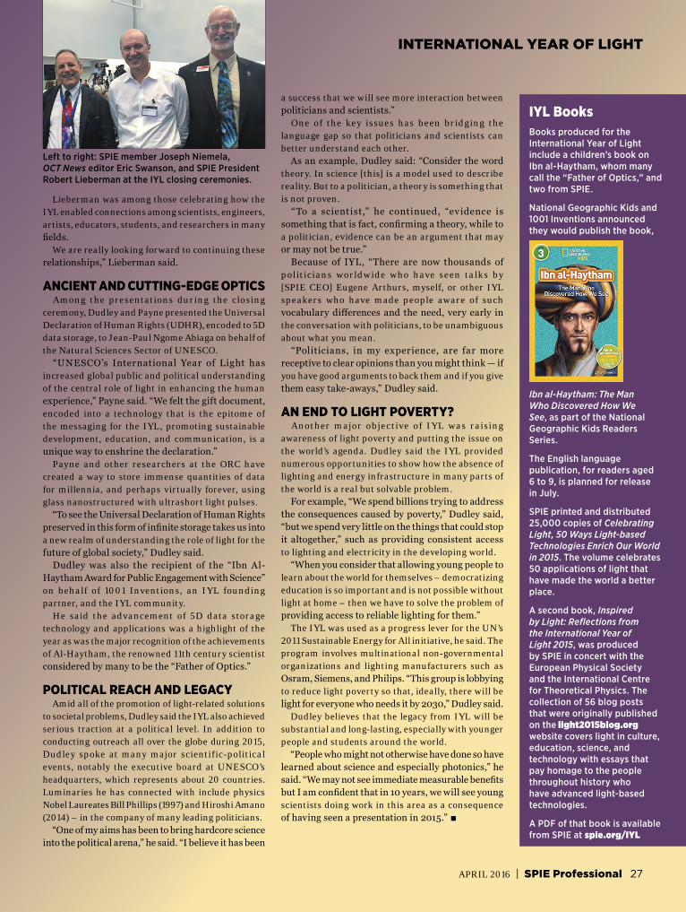
27APRIL 2016 | SPIE Professional
IYL Books Books produced for the International Year of Light include a children’s book on Ibn al-Haytham, whom many call the “Father of Optics,” and two from SPIE.
National Geographic Kids and 1001 Inventions announced they would publish the book,
INTERNATIONAL YEAR OF LIGHT
Lieberman was among those celebrating how the IYL enabled connections among scientists, engineers, artists, educators, students, and researchers in many fields. We are really looking forward to continuing these relationships,” Lieberman said.
ANCIENT AND CUTTING-EDGE OPTICS Among the presentations during the closing ceremony, Dudley and Payne presented the Universal Declaration of Human Rights (UDHR), encoded to 5D data storage, to Jean-Paul Ngome Abiaga on behalf of the Natural Sciences Sector of UNESCO. “UNESCO’s International Year of Light has increased global public and political understanding of the central role of light in enhancing the human experience,” Payne said. “We felt the gift document, encoded into a technology that is the epitome of the messaging for the IYL, promoting sustainable development, education, and communication, is a unique way to enshrine the declaration.” Payne and other researchers at the ORC have created a way to store immense quantities of data for millennia, and perhaps virtually forever, using glass nanostructured with ultrashort light pulses. “To see the Universal Declaration of Human Rights preserved in this form of infinite storage takes us into a new realm of understanding the role of light for the future of global society,” Dudley said. Dudley was also the recipient of the “Ibn Al-Haytham Award for Public Engagement with Science” on behalf of 1001 Inventions, an IYL founding partner, and the IYL community. He said the advancement of 5D data storage technology and applications was a highlight of the year as was the major recognition of the achievements of Al-Haytham, the renowned 11th century scientist considered by many to be the “Father of Optics.”
POLITICAL REACH AND LEGACY Amid all of the promotion of light-related solutions to societal problems, Dudley said the IYL also achieved serious traction at a political level. In addition to conducting outreach all over the globe during 2015, Dudley spoke at many major scientific-political events, notably the executive board at UNESCO’s headquarters, which represents about 20 countries. Luminaries he has connected with include physics Nobel Laureates Bill Phillips (1997) and Hiroshi Amano (2014) – in the company of many leading politicians. “One of my aims has been to bring hardcore science into the political arena,” he said. “I believe it has been
a success that we will see more interaction between politicians and scientists.” One of the key issues has been bridging the language gap so that politicians and scientists can better understand each other. As an example, Dudley said: “Consider the word theory. In science [this] is a model used to describe reality. But to a politician, a theory is something that is not proven. “To a scientist,” he continued, “evidence is something that is fact, confirming a theory, while to a politician, evidence can be an argument that may or may not be true.” Because of IYL, “There are now thousands of politicians worldwide who have seen talks by [SPIE CEO] Eugene Arthurs, myself, or other IYL speakers who have made people aware of such vocabulary differences and the need, very early in the conversation with politicians, to be unambiguous about what you mean. “Politicians, in my experience, are far more receptive to clear opinions than you might think — if you have good arguments to back them and if you give them easy take-aways,” Dudley said.
AN END TO LIGHT POVERTY? Another major objective of IYL was raising awareness of light poverty and putting the issue on the world’s agenda. Dudley said the IYL provided numerous opportunities to show how the absence of lighting and energy infrastructure in many parts of the world is a real but solvable problem. For example, “We spend billions trying to address the consequences caused by poverty,” Dudley said, “but we spend very little on the things that could stop it altogether,” such as providing consistent access to lighting and electricity in the developing world. “When you consider that allowing young people to learn about the world for themselves – democratizing education is so important and is not possible without light at home – then we have to solve the problem of providing access to reliable lighting for them.” The IYL was used as a progress lever for the UN’s 2011 Sustainable Energy for All initiative, he said. The program involves multinational non-governmental organizations and lighting manufacturers such as Osram, Siemens, and Philips. “This group is lobbying to reduce light poverty so that, ideally, there will be light for everyone who needs it by 2030,” Dudley said. Dudley believes that the legacy from IYL will be substantial and long-lasting, especially with younger people and students around the world. “People who might not otherwise have done so have learned about science and especially photonics,” he said. “We may not see immediate measurable benefits but I am confident that in 10 years, we will see young scientists doing work in this area as a consequence of having seen a presentation in 2015.” .
Left to right: SPIE member Joseph Niemela, OCT News editor Eric Swanson, and SPIE President Robert Lieberman at the IYL closing ceremonies.
Ibn al-Haytham: The Man Who Discovered How We See, as part of the National Geographic Kids Readers Series.
The English language publication, for readers aged 6 to 9, is planned for release in July.
SPIE printed and distributed 25,000 copies of Celebrating Light, 50 Ways Light-based Technologies Enrich Our World in 2015. The volume celebrates 50 applications of light that have made the world a better place.
A second book, Inspired by Light: Reflections from the International Year of Light 2015, was produced by SPIE in concert with the European Physical Society and the International Centre for Theoretical Physics. The collection of 56 blog posts that were originally published on the light2015blog.org website covers light in culture, education, science, and technology with essays that pay homage to the people throughout history who have advanced light-based technologies.
A PDF of that book is available from SPIE at spie.org/IYL
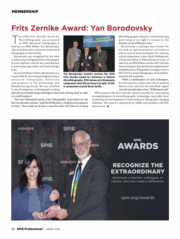
28 SPIE Professional | APRIL 2016
MEMBERSHIP
Frits Zernike Award: Yan Borodovsky
The 2016 Frits Zernike Award for Microlithography was presented at SPIE Advanced Lithography in
February to SPIE Fellow Yan Borodovsky, who retired last year as director of advanced lithography at Intel (USA). Borodovsky was recognized for his work in advancing multigenerational lithography process solutions and his key contributions to patterning approaches and layout design rules. As an Intel Senior Fellow, Borodovsky was responsible for directing multigenerational a d v a n c e d l i t h o g r a p h y d e f i n i t i o n and progress in the Technolog y and Manufacturing Group. He was involved in the development of lithography tooling and advanced patterning techniques since first joining Intel in 1987 as a staff engineer. “Yan has influenced nearly every lithographic innovation for the last two decades at least,” said David Shykind, a staff process engineer at Intel. “You could say he has a nose for what will allow us to keep
photolithography relevant to semiconducting patterning as we fight to remain on the density curve of Moore’s Law.” Borodovsky is perhaps best known for his work on optical proximity correction as well as several novel techniques for reducing critical dimensions, notes David Williamson, a Research Fellow at Nikon Research Corp. of America, an SPIE Fellow, and the 2007 Zernike Award recipient. Borodovsky has implemented complementary lithography strategies such as DUV, EUV, e-beam lithography, and template-directed self-assembly. “With a combination of such techniques, he will continue to play a key role in pushing Moore’s Law well into the sub-10nm region over the next decade or two,” Williamson said.
SPIE presents the Frits Zernike Award annually for outstanding accomplishments in microlithographic technology, especially those furthering the development of semiconductor lithographic imaging solutions. The award is sponsored by ASML and includes a $2,000 honorarium. .
Yan Borodovsky (center) receives the 2016 Frits Zernike Award for Advances in Optical Microlithography. SPIE Advanced Lithography symposium chair Mircea Dusa is at right. At left is symposium cochair Bruce Smith.
spie.org/awards
RECOGNIZE THE EXTRAORDINARYNominate a teacher, colleague, or
mentor who has made a difference.

29APRIL 2016 | SPIE Professional
MEMBERSHIP
White paper shows how PROCEEDINGSare crucial in getting research noticed
Proceedings publications offer advantages for researchers and companies
A new white paper from SPIE details how publishing in the right outlet puts research in front of potential collaborators who can be
key in commercializing new technology. Being first and getting noticed matter more than ever in an increasingly fast-paced and competitive global marketplace, according to the report, “The Value of Proceedings.” This applies to individuals sharing research findings as well as companies wanting to establish intellectual property rights. Publishing regularly in conference proceedings provides the discovery history for important new innovations, with findings reported as the research progresses. Besides illuminating the way forward for other researchers, proceedings papers also provide valuable information on what not to do, as inconclusive or negative results are included in the papers, and can enhance an individual’s professional status and potential career advancement. The report provides a comprehensive overview of the difference between publishing in journals vs. conference proceedings. Conference presentations reported in proceedings can help you: • Get feedback directly and instantly from your audience• Connect with other researchers and industry representatives• Make your published presentation available to those who heard your
work and want to contact you, missed your presentation and want to learn about your research, or are seeking to understand your research more fully
A proceedings paper can then be submitted with minimal or no revision for consideration in an appropriate SPIE journal.
PUBLISHING WITH SPIE Publishing in a widely indexed library among many other papers in the same field is also important. Proceedings of SPIE, published in the SPIE Digital Library, are strong in both regards, the report explains. Papers are indexed in Web of Science, Scopus, Ei Compendex, SAO/NASA Astrophysics Data System, Inspec, and other databases. The SPIE Digital Library collection of proceedings papers includes more than 410,000 articles in fields
across optics and photonics, including numerous multidisciplinary topics such as metrology, microelectronics, astronomy, biomedical and electronic imaging, nanotechnology, defense, and security. Thousands of new proceedings papers are added each year. The white paper cites user comments and industry data that show the effectiveness and usefulness of publishing with SPIE. For example, Proceedings of SPIE have been listed among the 50 most-used out of 50,000 serials analyzed by Ex Libris, a provider of library automation software. Of the top 40 patenting companies in the most recent analysis of US patents, 28 companies cite SPIE publications significantly. Industry leaders such as Apple, Bosch, Intel, Microsoft, Samsung Electronics, Toyota Motor Corp., and others are among those whose patent applications frequently cite SPIE proceedings. The white paper is available at: spie.org/ValueProceedings. .
SPIE election candidates named
Boreman
Giger
Lieberman
The SPIE Board of Directors has approved the following election slate for the Society’s 2016 election. Online
voting will be held 6 July through 18 August. SPIE members eligible to vote will select four new directors, a vice president, and a secretary/treasurer. Directors serve three-year terms and officers serve for one year.
THE CANDIDATES FOR VICE PRESIDENT ARE:• Harry Levinson,
GLOBALFOUNDRIES (USA)• Jim Oschmann, Ball Aerospace &
Technologies (USA)
THE CANDIDATE FOR SECRETARY/TREASURER IS:• Gary Spiegel, a consultant and retired
Newport executive (USA)
ON THE BALLOT FOR THE SPIE BOARD OF DIRECTORS ARE:• John Gonglewski, European Office of
Aerospace R&D (UK)• Wilhelm Kaenders, TOPTICA
Photonics (Germany)• Bernard Kress, Microsoft (USA)• Burn Lin, Taiwan Semiconductor
Manufacturing (Taiwan)• David Sampson, University of Western
Australia• Joanna Schmit, Bruker Nano Surfaces
(USA)• Christina Willis, Fibertek (USA)• Andrew Wood, Qioptiq (UK) Other officers with terms beginning 1 January 2017 were previously elected: SPIE President-Elect Glenn Boreman of University of North Carolina at Charlotte and Plasmonics
Inc. (USA) will become SPIE president, and SPIE Vice President Maryellen Giger of University of Chicago (USA) becomes president- elect next year. SPIE President Robert Lieberman of Lumoptix (USA) will become immediate past president. Election results will be announced at the SPIE annual general meeting in San Diego (USA) 30 August. .

30 SPIE Professional | APRIL 2016
MEMBERSHIP
Thirty-three SPIE members have been named Fellows of the Society this year. The honor recognizes their significant scientific and technical contributions in the multidisciplinary
fields of optics, photonics, and imaging as well as their service to the Society and the greater community. The new SPIE Fellows are now among more than 1000 who have been named since the Society was founded in 1955. “Our new Fellows exemplify the full diversity of the photonics community,” said SPIE Fellows Committee chair Majid Rabbani. “They truly are an elite group. I congratulate them all for their outstanding contributions and am honored to associate with these impressive researchers and innovators.” SPIE President Robert Lieberman joined in congratulating the 2016 SPIE Fellows. “Each of the distinguished individuals being recognized this year as Fellows of SPIE has served the society admirably,” Lieberman said, “whether through organizing conferences, making
SPIE NAMES 33 NEW FELLOWSimportant and useful research available via their publications, sharing knowledge and skills as course instructors, mentoring the next generation, or numerous other ways. “They are among the most outstanding scientists, engineers, innovators, and visionaries in our field’s global community, and SPIE is enriched by their participation,” he said. “I congratulate each new Fellow, and look forward to following their further accomplishments.” New Fellows are recognized at SPIE meetings of their choice throughout the year, including Photonics West, Advanced Lithography, Medical Imaging, Smart Structures/NDE, Photonics Europe, Defense + Commercial Sensing, and Optics + Photonics. The deadline for nominating Fellows for 2017 is 15 September. New SPIE Fellows must be SPIE Senior Members. The deadline for nominating colleagues for Senior Member promotion is 15 April. More information: spie.org/fellows. .
Augusto BeléndezUniversidad de Alicante (Spain)
Eugene ArthursSPIE (USA)
Alexey BelyaninTexas A&M University (USA)
Bernard ChoiBeckman Laser Institute and Medical Clinic (USA)
Laurence ClarkeNational Cancer Institute (USA)
Thomas CooleyAir Force Research Lab (USA)
Jürgen CzarskeTechnische Universität Dresden (Germany)
Peter DelfyettUniversity of Central Florida (USA)
Armin DoerrySandia National Labs (USA)
Jason EichenholzOpen Photonics (USA)
Andreas ErdmannFraunhofer IISB (Germany)
Rinat EsenalievUniversity of Texas Medical Branch (USA)
Stephen FantoneOptikos (USA)
Joseph HowardNASA Goddard Space Flight Center (USA)
Ilko IlevUS Food and Drug Administration (USA)
Richard JuergensRaytheon Missile Systems (USA)
Dennis KillingerUniversity of South Florida (USA)
Guoqiang LiOhio State University (USA)
Jean-Christophe Olivo-MarinInstitut Pasteur (France)
Richard PfistererPhoton Engineering (USA)

31APRIL 2016 | SPIE Professional
MEMBERSHIP
SPIE is the international society for optics & photonics.
Membership
Are you maximizing your Membership?CAN YOU PUT A “CHECK MARK” IN THE BOX
P Reading SPIE Professional
Downloading 10 Digital Library articles or proceedings annually
Reading online journal subscription
Getting discounts on publications, courses, and conference registrations
Keeping profile up-to-date
Accessing online course
www.spie.org/coursesRenew your investment anytimewww.spie.org/[email protected]+1 360 676 3290A
Gary PickrellVirginia Polytechnic Institute and State University (USA)
Mary PotasekSimphotek (USA)
Ingmar RenhornRenhorn IR Consultant (Sweden)
Kurt Ronseimec (Belgium)
Peter SchunemannBAE Systems (USA)
Peter SoMassachusetts Institute of Technology (USA)
Martin StickleyConsultant (USA)
Robert ThomasAir Force Research Lab (USA)
Monte TurnerAir Force Research Lab (USA)
Michael WangUniversity of Miami (USA)
Changhuei YangCalifornia Institute of Technology (USA)
George ZentaiVarian Medical Systems (USA)
Xuejun ZhangChangchun Institute of Optics, Fine Mechanics and Physics (China)
SPIE AWARD AND FELLOW NOMINATIONSNominations are open for annual SPIE awards and for the next class of SPIE Fellows. More information on SPIE awards is at spie.org/awards
The deadline for nominating a colleague for promotion to SPIE Fellow is 15 September 2016. Information on eligibility and other criteria for 2017 Fellows is at spie.org/fellows
32 SPIE Professional | APRIL 2016
Moving from a small research team at a European prime defense contractor to the UK’s national meteorological service seemed like a radical job change when I made
the move a few years ago. Swapping photonics R&D for building relationships between the Met Office and its international defense partners looked like a sideways career move that would take me away from photonics. However, nothing could be further from the truth. My role today, at the world’s oldest meteorological service, is to bridge the gap between the needs of defense personnel who use infrared sensors to plan missions and the capabilities of the Met Office to predict the impacts of the weather on those sensors. In doing so, my knowledge of photonics aids the decision making of people who exploit such sensors for military and civilian applications. Much of my role involves convincing researchers in labs at partner governments that the weather is an important aspect to be considered from the outset, during design stages. My first-hand experience of their industry allows for an easy dialogue, and my initial lack of formal meteorological training is actually an advantage, as I can alert the sensor engineers to issues that I had encountered myself. At the same time, because I can approach such environmental issues from the perspective of a photonics engineer rather than a meteorologist, I can easily interface between the Met Office’s internal stakeholders in weather forecasting and external collaborators. My ability to articulate the requirements of these photonics engineers means I am well placed to match their needs to the weather forecasting capabilities of the Met Office.
EMPLOYMENT OPTIONS GROW I provide some examples below of projects where I have leveraged my two seemingly separate careers in such a way as to provide an enhanced outcome. Such an approach would have been difficult to instigate without a firm footing in both the defense-photonics and weather-forecasting communities. As I learned, developing skills in an entirely new scientific field can often involve a steep learning curve. However, it can bring vast benefits to both the engineer in question and to the employer — especially if opportunities to network and collaborate are actively encouraged. Photonics engineers with diversified backgrounds have many more employment options and opportunities for advancement, especially if they want to remain relatively close to their preferred specialization. Here are selected top tips from my experience in bringing photonics into what may seem like an unrelated sector:• Stress the advantages that your photonics experience can bring to
the new sector.• Maintain your network in the photonics community and keep up to
date in the field.• Use humility in your new position but don’t hesitate to offer ideas
on how photonics can enhance your projects. As a photonics engineer, you’ll bring novel insights and knowledge
Weathering a change in careerCAREER
that can generate new opportunities in your new sector. When and if your lack of experience in the new sector comes to attention, highlight your experience in photonics and show how you could tackle problems from a new perspective. The diversity that you bring is an advantage because you can explore new ways to solve problems and make otherwise unlikely and revolutionary advances. Leverage past networks and keep attending conferences such as those sponsored by SPIE to maintain connections and keep abreast of developments in the field. Being aware of and current on recent photonic developments is a must to maintain credibility. Creating new business relationships can be a challenge, at least early on in a new role. But it can be easier if you prepare for occasions when you can show your new colleagues the problem-solving capabilities of photonics. Be humble in your new field but voracious in consuming the new knowledge that will come your way. Stimulate internal discussion with any novel or interesting links between photonics and the new sector with which you’re engaged. Become a catalyst for ideas and new ways of thinking, especially when planning a project from beginning to end.
FORECASTING TOOL FOR ENGINEERS One prime example of the Met Office capability to support the defense community is our NEON tactical decision aid (TDA) that I primarily promote to NATO and coalition partners. NEON is a web-based tool for predicting the thermal contrast of land and maritime targets with respect to their local backgrounds. It all starts with the ingestion of over 10 million daily observations by air, land, sea, space, and cyberspace from Met Office assets and those of World Meteorological Organization (WMO) partners. These data, combined with the modeling efforts of several hundred scientists at our UK headquarters, allow our supercomputer to generate over 3000 tailored forecasts and briefings per day. The economic sectors that benefit from our forecasts range from traditional transportation industries (road, rail, air, and maritime) to new areas such as reinsurance and derivatives, plus supermarkets and renewable energy companies. Our new 24/7 Space Weather Operations Centre is also stimulating interest across many areas related to critical infrastructure, such as power grids, communications, and GPS-time-stamped financial trading. The NEON tool takes our global forecasts and applies our models of the atmosphere and target environment to account for weather effects on thermal contrasts across land and maritime domains. The tool can account for moving targets relative to the wind; different viewing angles; and even the effects of a spherical planet on radiative transfer when predicting acquisition ranges. While aimed at mission planners and aircrew in the defense sector, NEON can also be exploited during detailed real-world sensor testing and trials by civilian photonics engineers in many sectors. More effort has gone into validation and verification than into the software
SOMETIMES, A CAREER TRANSITION CAN BE A BREEZE By Gerald J. Wong

33APRIL 2016 | SPIE Professional
CAREER
development of NEON itself, as assurance is an extremely important factor for defense end-users.
BETTER THAN ‘AVERAGE’ FORECAST In order to connect to sensor designers, I needed output that was more simplified (but not simple) than detailed Time +36-hour (T+36) thermal contrast predictions. From discussions at conferences such as SPIE, I deduced a need for representative weather information across certain key regions of interest such as the Middle East. Long-standing “standard” atmospheric profiles were too simplistic for engineers in the early stages of prototype design, but my combined photonics knowledge and increased experience in the meteorological domain allowed me to develop the concept of “Historical-Regional Analysis” (HRA). HRA takes past observations, or T+0 forecasts, across a region of interest and clusters them in terms of weather classifications (precipitation intensity, visibility limiters, and thermal profiles) and geographical domains (littoral, open-seas, inland, mountainous, etc.). Combining these with statistical processing (guided by meteorologist expertise), we can generate “representative days” of weather for a specific region. This type of analysis is more rigorous than calculating simple scalar “averages” at a single point in space (and often time) of what is essentially a chaotic, non-linear, and dynamic phenomenon. The result is a meteorologically valid dataset for the testing of sensor concepts.
WIN-WIN CAREER MOVE I hope my experiences have shown it is possible to switch career paths and prosper, leveraging past knowledge to your advantage. It
may well be that anyone undertaking such a transition will become the leading authority or “go to” person for photonics within the new home organization, regardless of past position or specific role. Being valued as an expert and having the opportunity to bridge the gap is ultimately a good thing for you, your employer, and both scientific communities involved.
–Gerald J. Wong is an international defense R&D capability exploitation adviser at the UK Met Office. He earned a doctorate in engineering at Heriot-Watt University (UK) and has master’s degrees in physics and business administration. Wong, a chartered engineer and chartered physicist, is a member of the Institution of Engineering and Technology and the Institute of Physics. He joined the Met Office in late 2013. .
Wong and space weather advisor Helen Waite at the Met Office Space Weather Operations Centre.
Inside the MET Office.
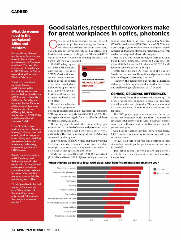
34 SPIE Professional | APRIL 2016
What do womenneed in the workplace?Allies and mentorsHaving strong allies or mentors can help women in workplaces where inclusiveness isn’t always practiced. That was the consensus of panelists at an SPIE Women in Optics event during Photonics West in February.
The discussion about trends in female participation in the technology sector was moderated by Lina Nilsson of Enlitic and University of California, Berkeley and included Rachel Thomas of Hackbright Academy, Y-Vonne Hutchinson of ReadySet, Karla Monterroso of CODE2040, and Omoju Miller of Learners Guild.
“I don’t think people realize how much Rome is burning,” Monterroso said about the slow progress in recruiting and retaining women and minorities in science, technology, engineering, and math (STEM) roles.
Panelists and discussion participants agreed that women must take ownership of the problem and make a conscious commitment to create an inclusive culture in the workplace, especially by mentoring each other.
“It is imperative to be that resource for someone else,” Hutchinson told the standing-room-only crowd. “If you’re in the position to mentor, mentor.”
Good salaries, respectful coworkers makefor great workplaces in optics, photonics
When thinking about your ideal workplace, what benefits are most important to you?
0 20% 40% 60% 80% 100%
Flexibility to work remotely
Ability to travel
Paid parental leave
Opportunity for continuing education
Employer-provided health insurance
Paid sick leave
Sense of community
High pay
Paid Vacation
Flexible work hours
Opportunity for advancement
Respect from co-workers
WHEN THINKING ABOUT YOUR IDEAL WORKPLACE, WHAT BENEFITS ARE MOST IMPORTANT TO YOU?
Important
Very Important
CAREER
Of f ices and laboratories for optics and photonics professionals are great places to work because of the respect from coworkers,
opportunity for advancement, paid vacation, and flexible work hours, according to the 6th annual SPIE Optics & Photonics Global Salary Report. And it’s a bonus that the pay is so good. The 2016 salary report, mailed to SPIE members with the April issue of SPIE Professional, shows respect from coworkers ranked as the top benefit of an ideal workplace, followed by opportunity f o r a d v a n c e m e n t , flexible work hours, paid vacation, and high pay in fifth place. The median salary for full-time employees in optics and photonics is $62,443, according to the new SPIE report, down slightly from $64,000 in 2015. The aerospace sector was again found to offer the highest median salaries, $102,300. The survey also showed other areas of high job satisfaction in the field of optics and photonics, with 96% of respondents saying they enjoy their work, 95% finding their work meaningful, and 93% feeling respected by their peers. Salaries in the field are widely dispersed, varying by region, country economic conditions, gender, employer type, total years employed, and primary discipline within optics and photonics. Workers in the United States ($112,000), Switzerland ($110,351), and Israel ($85,822) have the highest median
salaries, according to the report, followed by Australia ($79,830), Netherlands ($78,268), Japan ($74,509), and Germany ($70,659). Broken down by regions, North America and Oceania offered the highest salaries, with median earnings well above other regions. Median pay was lowest among workers in China, Poland, India, Romania, Russia, and Ukraine, with a low of $2,740 a year in Ukraine and $5,520 for all lower-income countries in Europe. SPIE CEO Eugene Arthurs said the survey “confirms the health of the optics and photonics field even as the global economy sputters.” However, the gender pay gap “is still a disgrace, although the history of male domination in science and engineering explains part of it,” he said.
GENDER, REGIONAL DIFFERENCES The survey found that women, who made up 17% of the respondents, continue to earn less than men overall in optics and photonics. The median annual salary for women was $48,000, compared to $66,240 for men. The 38% gender gap is much smaller for early-career professionals with less than five years of employment, however, and reversed in lower-income countries in Europe and in civilian, non-research government jobs. Asked about whether they feel they are paid fairly, 69% of women responding to the survey said yes, vs. 76% of men. Arthurs said future surveys will continue to look at whether there is gender parity for recent entrants to the field. Two other factors driving salary gaps across disciplines are employment sector and country income level.
35APRIL 2016 | SPIE Professional
Education
GETSMARTER•
Technology advances on a daily basis.
HOW WILL YOU KEEP UP?
Continue your education and training at your convenience. Courses taught by experts.
LIVEINSTRUCTION
DISTANCEEDUCATION
COURSES AT EVENTS PIN-COMPANY TRAINING PONLINE COURSES PDVDS P
For more information, visit: www.spie.org/courses
CAREER
The survey found the highest-paying disciplines have much higher representations at for-profit companies. For example, of the people working in the top three disciplines by pay (aerospace, illumination, and semiconductor), 401 work at for-profit organizations vs 96 in government or the military, and 75 in academia. Other key findings from the survey that was administered in January:• Salaries paid in Chinese yuan declined 1% over the last year,
following a gain of 33% from 2012 through 2015.• Earnings in Japanese yen and British pounds were up, while salaries
paid in US dollars and euros were flat.• Workplace challenges most frequently faced by respondents are lack
of advancement opportunities and not enough time with family. The survey also found that entry-level pay for PhDs is highest in the US, where employees with 1 to 2 years of experience earn a median salary of $73,000. Germany, the UK, and South Korea follow, with respective salaries of $58,701, $44,031, and $41,400. Of the 6793 valid responses in the salary survey, 4744 respondents worked full time, 237 worked part time, and 1812 were students.
BENEFITS SOMETIMES INTANGIBLE Early results of the survey were presented at SPIE Photonics West in February where a panel of early-career professionals working in industry agreed that coworkers’ passion, teamwork, and collegiality make for an excellent work environment. Coworkers show their respect for each other by being reliable and willing to help others solve problems, even when not assigned to a project, the panelists said. “I am doing my best when I know someone is depending on me,” said SPIE member Nishant Mohan, director of product management and marketing at Wasatch Photonics’ Systems Division. SPIE member Christina Willis, a laser scientist at Fibertek who was also on the panel, added, “You can love your work, but if your co-workers are mean to you, you’re going to hate going to work.” The third panelist, Aaron Weinroth, vice president of technology commercialization at Tornado Spectral Systems, said he was a bit surprised that high pay was ranked only fifth on the list of top work benefits, especially since an employer doesn’t control relationships among coworkers. Still, Weinroth said, employers need to foster a culture of mutual respect and provide opportunities for professional development. “People have to show respect for each other,” he said. Indeed, Arthurs commented that the “intangible rewards of being in optics and photonics do not show up in our survey. These include having knowledge and skills for a field with a very bright future, and for many, the satisfaction in contributing to enhancing life on our planet.” The salary report is available online at SPIEcareerCenter. .
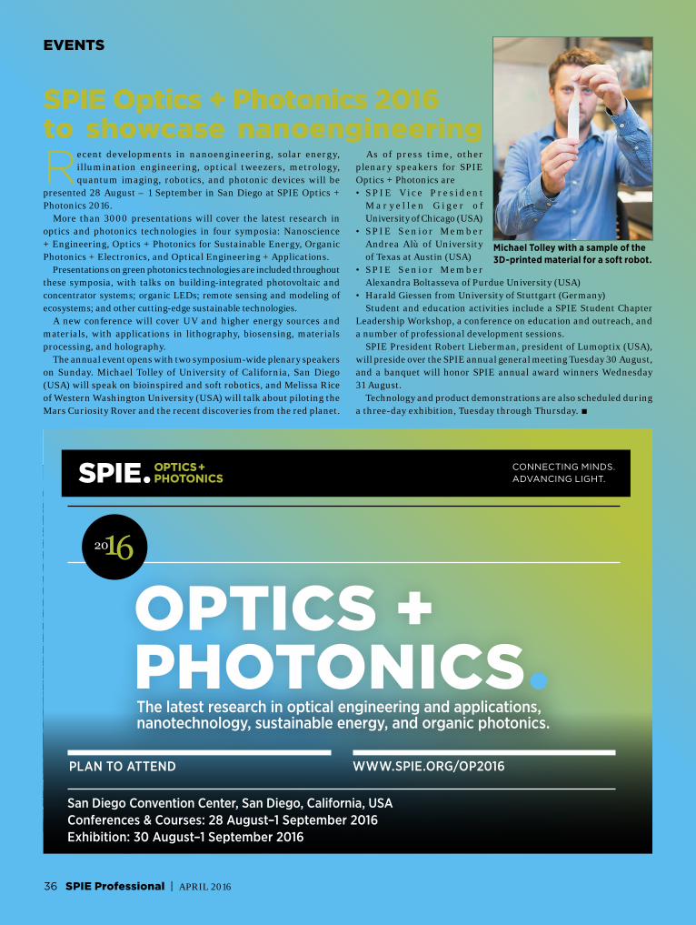
36 SPIE Professional | APRIL 2016
EVENTS
The latest research in optical engineering and applications, nanotechnology, sustainable energy, and organic photonics.
PLAN TO ATTEND WWW.SPIE.ORG/OP2016
OPTICS + PHOTONICS•
CONNECTING MINDS. ADVANCING LIGHT.
San Diego Convention Center, San Diego, California, USAConferences & Courses: 28 August–1 September 2016Exhibition: 30 August–1 September 2016
SPIE Optics + Photonics 2016to showcase nanoengineering Recent developments in nanoengineering, solar energy,
illumination engineering, optical tweezers, metrology, quantum imaging, robotics, and photonic devices will be
presented 28 August – 1 September in San Diego at SPIE Optics + Photonics 2016. More than 3000 presentations will cover the latest research in optics and photonics technologies in four symposia: Nanoscience + Engineering, Optics + Photonics for Sustainable Energy, Organic Photonics + Electronics, and Optical Engineering + Applications. Presentations on green photonics technologies are included throughout these symposia, with talks on building-integrated photovoltaic and concentrator systems; organic LEDs; remote sensing and modeling of ecosystems; and other cutting-edge sustainable technologies. A new conference will cover UV and higher energy sources and materials, with applications in lithography, biosensing, materials processing, and holography. The annual event opens with two symposium-wide plenary speakers on Sunday. Michael Tolley of University of California, San Diego (USA) will speak on bioinspired and soft robotics, and Melissa Rice of Western Washington University (USA) will talk about piloting the Mars Curiosity Rover and the recent discoveries from the red planet.
As of press t ime, other plenary speakers for SPIE Optics + Photonics are• S P I E V i c e P r e s i d e n t
M a r y e l l e n G i g e r o f University of Chicago (USA)
• S P I E S e n i o r Me m b e r Andrea Alù of University of Texas at Austin (USA)
• S P I E S e n i o r Me m b e r Alexandra Boltasseva of Purdue University (USA)
• Harald Giessen from University of Stuttgart (Germany) Student and education activities include a SPIE Student Chapter Leadership Workshop, a conference on education and outreach, and a number of professional development sessions. SPIE President Robert Lieberman, president of Lumoptix (USA), will preside over the SPIE annual general meeting Tuesday 30 August, and a banquet will honor SPIE annual award winners Wednesday 31 August. Technology and product demonstrations are also scheduled during a three-day exhibition, Tuesday through Thursday. .
Michael Tolley with a sample of the 3D-printed material for a soft robot.

37APRIL 2016 | SPIE Professional
EVENTS
Workshop in Texas focuseson biophotonics commercializationThe second SPIE Translational Biophotonics workshop will
be held 16-17 May in Houston at Rice University (USA). This interdisciplinary forum brings practicing clinicians together
with experts in academia and industry to encourage the continuing development of new technologies and techniques for successful translation into practical biomedical use. Oral and poster presentations will focus on optical diagnostics, image-guided intervention, novel microscopy techniques, new biomedical probes, and system design and implementation. Applications include cancer diagnostics, cardiovascular imaging, detection of infectious disease, and applications in primary and point of care. In a session on commercial translation, leaders in biophotonics will discuss the path of new technologies from startup to maturity. Participants include Caroline Boudoux, cofounder of Castor Optics and professor at Ecole Polytechnique de Montréal (Canada); SPIE Fellow Alexander Oraevsky, president and CTO of TomoWave Labs (USA); SPIE Senior Member Milind Rajadhyaksha of Memorial Sloan Kettering Cancer Center (USA); and Stephan Briggs, biomedical product line engineer at Edmund Optics (USA). Top biophotonics experts and entrepreneurs will discuss their latest advancements and plot new directions for the future of optical imaging
for both research and clinical applications. Clinicians will present their perspectives on application needs, and industry representatives will discuss pathways to commercialization. Inv ited speakers include SPIE Fellows Stephen Boppart of University of Illinois at Urbana-Champaign (USA), David Dickensheets of Montana State University (USA), Xingde Li of Johns Hopkins University (USA), Bruce Tromberg of Beckman Laser Institute, University of California, Irvine (USA), and Adam Wax of Duke University (USA). Also giving invited talks are SPIE members Adela Ben-Yakar of University of Texas at Austin (USA), Brian Pogue of Dartmouth College (USA), and Melissa Skala of Vanderbilt University (USA). Chair ing SPIE Translat iona l Biophotonics 2016 is SPIE Fellow Tomasz Tkaczyk of Rice University, which is cosponsoring the event. More information: spie.org/TBP. .
Abstracts Due: 18 July 2016Call for Papers
Conferences & Courses: 28 January–2 February 2017Photonics West Exhibition: 31 January–2 February 2017BiOS EXPO: 28–29 January 2017
www.spie.org/pw2017
The Moscone Center San Francisco, California, USA
PHOTONICSWEST•THE PREMIER EVENT FOR THE PHOTONICS AND LASER INDUSTRIES
SPIEDigitalLibrary.org
Find the Answer
Sensors
38 SPIE Professional | APRIL 2016
EVENTS
Asia’s premier event on nanophotonics, biophotonics, lasers, optical design, plasmonics, sensors, optoelectronics, infrared/terahertz, and more.
CALL FOR PAPERS WWW.SPIE.ORG/PA2016
PHOTONICS ASIA•
CONNECTING MINDS. ADVANCING LIGHT.
Beijing International Convention Center, Beijing, China Conferences: 12–14 October 2016
SPIE DCS program features very BIG and very small technologiesPresentations on miniature robots, sensors, and satellites will
complement a large variety of conferences and courses on technologies for monitoring vast expanses of ocean and space,
providing disaster relief, and processing big data at SPIE Defense + Commercial Sensing (DCS) in Baltimore, MD, 17-21 April. The annual event for the defense and commercial sensing communities, previously called SPIE DSS, will include 56 technical conferences, 35 courses, a three-day exhibition, job fair 20 April, and industry seminars, workshops, and panel discussions. A symposium-wide plenary session 18 April will feature two speakers: Bradford Tousley, director of the Tactical Technology Office at the US Defense Advanced Research Projects Agency (DARPA), and Patrick Carrick, director of the US Homeland Security Advanced Research Project Agency (HSARPA). Special events include a panel discussion on the growing use of CubeSats, small 10x10x10 cm cubic satellites that are revolutionizing Earth observations from space; demonstrations of the capabilities of drones and a presentation on the rules of flying them; and a keynote talk on sensor-information extraction by William Chappell, deputy director of DARPA’s Microsystems Technology Office.
In addition, SPIE will provide updates on the size of the photonics market in the defense sector and on newly proposed US rules on exporting products that could be considered munitions. SPIE DCS includes two symposia in the Baltimore Convention Center. The SPIE Defense + Security symposium includes conferences on imaging and image processing, sensors, robotics, energy harvesting, big-data analytics, biometrics, pattern and target recognition, display technologies, lasers, ocean sensing, and other optics and photonics topics. SPIE member David Logan of BAE Systems is chair. Donald Reago Jr. of the US Army Night Vision & Electronic Sensors Directorate is cochair. SPIE Commercial + Scientific Sensing and Imaging, featuring conferences on sensor technologies driving new commercial applications in health care, pharmaceuticals, industrial processing, manufacturing, communications, agriculture, and transportation, is chaired by Ming Wu of University of California, Berkeley (USA). Cochair is SPIE Fellow Majid Rabbani of Eastman Kodak (USA) who is the featured speaker at the SPIE Fellows luncheon. More information: spie.org/DCS. .
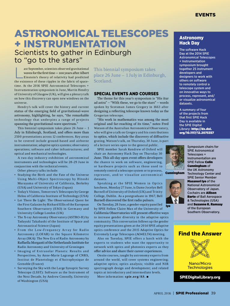
39APRIL 2016 | SPIE Professional
EVENTS
Astronomy Hack Day The software Hack Day at the 2014 SPIE Astronomical Telescopes + Instrumentation symposium brought together 25 instrument developers and designers to work with others on software to remotely control a telescope system and on innovative ways to process, represent, and/or visualize astronomical datasets.
A summary of four of the projects from that first SPIE Hack Day is available in the SPIE Digital Library: http://dx.doi.org/10.1117/12.2075357
ASTRONOMICAL TELESCOPES + INSTRUMENTATIONScientists to gather in Edinburgh to “go to the stars”
Last September, scientists observed gravitational waves for the first time — 100 years after Albert Einstein’s theory of relativity had predicted
the existence of these ripples in the fabric of space-time. At the 2016 SPIE Astronomical Telescopes + Instrumentation symposium in June, Martin Hendry of University of Glasgow (UK), will give a plenary talk on how this discovery can open new windows on the universe. Hendry’s talk will cover the history and current status of the emerging field of gravitational-wave astronomy, highlighting, he says, “the remarkable technology that underpins a range of projects spanning the gravitational-wave spectrum.” This biennial symposium takes place 26 June – 1 July in Edinburgh, Scotland, and offers more than 2500 presentations across 12 conferences. Key areas to be covered include ground-based and airborne instrumentation; adaptive optics systems; observatory operations; software and cyber infrastructures; and optical and mechanical technologies. A two-day industry exhibition of astronomical instruments and technologies will be 28-29 June in conjunction with the technical events. Other plenary talks include:• Studying the Birth and the Fate of the Universe
Using Multi-Object Spectroscopy by Hitoshi Murayama of University of California, Berkeley (USA) and University of Tokyo (Japan)
• Today’s Visions, Tomorrow’s Telescopes by George Helou of California Institute of Technology (USA)
• Let There Be Light: The Observational Quest for the First Galaxies by Richard Ellis of the European Southern Observatory (ESO) in Germany and University College London (UK)
• The X-ray Astronomy Observatory (ASTRO-H) by Tadayuki Takahashi of the Institute of Space and Astronautical Science (Japan)
• From the Low-Frequency A rray for Radio Astronomy (LOFAR) to the Square Kilometre Array (SKA): The New Era of Radio Astronomy by Raffaella Morganti of the Netherlands Institute for Radio Astronomy and University of Groningen
• Imaging of Extrasolar Planets: Results and Perspectives, by Anne-Marie Lagrange of CNRS, Institut de Planetology et d’Astrophysique de Grenoble (France)
• Surveying the Sky with the Large Synoptic Survey Telescope (LSST): Software as the Instrument of the Next Decade, by Andrew Connolly, University of Washington (USA)
SPECIAL EVENTS AND COURSES The theme for this year’s symposium is “His itur ad astra” – “With these, we go to the stars” – words spoken by Scotsman James Gregory in 1663 after designing a reflecting telescope known today as the Gregorian telescope. “His work in mathematics was among the most original and far-reaching of its time,” notes Fred Watson of the Australian Astronomical Observatory, who will give a talk on Gregory and his contributions to optics, which include the discovery of diffractive grating. Watson’s talk, on Thursday, 30 June, is part of a lecture series open to the general public. SPIE member Sarah Kendrew of Oxford will chair an Astronomy Hack Day on Thursday 30 June. This all-day open event offers developers the chance to work on software, engineering, or hardware projects such as those used to remotely control a telescope system or to process, represent, and/or v isualize astronomical datasets. Speaking at the SPIE Women in Optics luncheon, Monday 27 June, is Dame Jocelyn Bell Burnell of University of Oxford (UK) and Trinity College, Dublin. As a postgraduate in 1967, Bell Burnell discovered the first radio pulsars. On Tuesday, 28 June, a gender-equity panel led by SPIE Fellow Claire Max of the University of California Observatories will present effective ways to increase gender diversity in the adaptive optics community. This conversation follows up the gender equity presentations given at the 2014 SPIE adaptive optics conference and the 2015 Adaptive Optics for Extremely Large Telescopes (AO4ELT4) meeting. Also on Tuesday, SPIE offers a lunch with the experts to students who want the opportunity to network with optics and photonics experts as they offer advice and share their career experiences. Onsite courses, taught by astronomy experts from around the world, will cover systems engineering; adaptive optics; optics analysis; visible and NIR spectrograph design and development; and related topics at introductory and intermediate levels. More information: spie.org/AS. .
Symposium chairs for SPIE Astronomical Telescopes + Instrumentation are SPIE Fellow Colin Cunningham of the UK Astronomy Technology Center and SPIE Senior Member Masanori Iye of the National Astronomical Observatory of Japan. Cochairs are Allison Barto of Ball Aerospace & Technologies (USA) and Suzanne K. Ramsay of the European Southern Observatory.
Cunningham
Iye
This biennial symposium takes place 26 June – 1 July in Edinburgh, Scotland.
SPIEDigitalLibrary.org
Find the Answer
Nano/Micro Technologies

Upcoming events and deadlines Check your monthly SPIE Member E-news for more information on and links to the items below.
ADVERTISER INDEXAccu-Glass Products 19www.accuglassproducts.com
Applied Optics Research . . . . . .Cover 2www.aor.com
LaCroix Optical . . . . . . 7www.lacroixoptical.com
Photon Engineering . . 15www.photonengr.com
Software Spectra . . . . 2www.sspectra.com
EVENTS AROUND THE WORLD
FOLLOW SPIE ON:
Find photos and daily summaries of many SPIE meetings online: spie.org/eventnews
SPIE Event News
SPIE EVENTSFind detailed information about SPIE conferences at spie.org/conferences
Create your schedule with the SPIE Conference App for iPhone and Android. The mobile app is available at spie.org/mobile and at the Android Market and AppStore.
APRIL 20163-7: SPIE Photonics Europe 4: Comment period ends on US export
regulations4-7: SPIE Asia-Pacific Remote Sensing6-8: Photomask Japan 12-13: Congressional Visits Day in
Washington, DC 15: Nominations due for SPIE Senior Member 17-21: SPIE Defense + Commercial Sensing18: Abstracts due for SPIE Biophotonics
Australasia 25: Abstracts due for SPIE Laser Damage 30: Abstracts due for UK Optical Design
MAY 201616: Abstracts due for SPIE/COS Photonics
Asia16-17: SPIE Translational Biophotonics17-20: OPIC 18-20: SPIE/SIOM Pacific Rim Laser Damage
JUNE 20161: Nominations due for SPIE awards 15-17: OPTO Taiwan 26–1 JULY: SPIE Astronomical Telescopes +
Instrumentation
JULY 20166: Electronic voting begins in SPIE 2016
election18: Abstracts due for SPIE Photonics West
2017
AUGUST 201618: Last day to vote in SPIE 2016 election28-1 SEPTEMBER: SPIE Optics + Photonics30: SPIE Annual General Meeting
2016
ASPIE AWARD AND FELLOW NOMINATIONSNominations are open for annual SPIE awards and for the next class of SPIE Fellows.
All nominations for the 2017 SPIE annual awards are due 1 June. A complete nomination packet includes a brief citation as well as a one-page narrative on the nominee’s accomplishments, a curriculum vitae, and at least two letters of reference from someone other than the nominator.
More information on SPIE awards is at spie.org/awards
The deadline for nominating a colleague for promotion to SPIE Fellow is 15 September 2016. Information on eligibility and other criteria for 2017 Fellows is at spie.org/fellows
SPIEDigitalLibrary.org
Find the Answer
Defense & Security
Read details and sample pages: www.spie.org/books
NEW BOOKS FROM SPIE
Publications
Design and Implementation of Autostereoscopic Displays Byoungho Lee, Jisoo Hong, Keehoon Hong, and Soon-gi ParkVol. TT99Print: $47 / $55 eBook: (PDF, ePub, Kindle) $40 / $47
Discrimination of Subsurface Unexploded Ordnance Kevin A. O’NeillVol. TT102Print: $56 / $66 eBook: (PDF, ePub, Kindle) $48 / $56
Molecular Theory of Lithography Uzodinma OkoroanyanwuVol. PM255Print: $78 / $92 eBook: (PDF, ePub, Kindle) $66 / $78
How to Set Up a Laser LabKen BaratVol. SL02
Image Resolution: Deconstructing Hollywood’s Zoom and EnhanceRobert D. FieteVol. SL01
Optical Sensing: Microstructured Fibers, Fiber Micromachining, and Functional CoatingsMinghong Yang, Dongwen Lee, and Yu-Tang DaiVol. SL03
eBooks available in PDF, ePub, Kindle SPIE Member $25 / Nonmember $31
LADAR Applications for Orbital Debris RemovalXiang ZhuVol. SL08
Optical Phantoms: Diffuse and Sub-diffuse Imaging and Spectroscopy ValidationGage J. Greening, Haley M. James, and Timothy J. MuldoonVol. SL09
Digital Endoscope Design Dennis C. Leiner Vol. SL10
Carbon Nanoparticles in Photoacoustic ImagingTi Zhang and Huizhong CuiVol. SL04
Optimization Techniques for Diffraction SpectrometersElena SokolovaVol. SL05
Femtosecond-Laser-Assisted LASIK Eye Surgery and ImagingHui SunVol. SL06
Raman Spectroscopy: Applications in Breast Cancer ManagementTanmoy Bhattacharjee and C. Murali KrishnaVol. SL07
All books are priced: SPIE Member / Nonmember
Design Technology Co-Optimization in the Era of Sub-Resolution IC Scaling Kaushik Vaidyanathan, Lars W. Liebmann, and Lawrence PileggiVol. TT104Print: $47 / $55 eBook: (PDF, ePub, Kindle) $40 / $47
Special Functions for Optical Science and Engineering L. S. Varadharajan and Vasudevan LakshminarayananVol. TT103Print: $63 / $74 eBook: (PDF, ePub, Kindle) $54 / $63
CONCISE, FOCUSED, AND PEER REVIEWED
New eBook Series
www.spie.org/journals
[email protected] Tel: +1 360 676 3290 Fax: +1 360 647 1445
- All SPIE Journals are part of the SPIE Digital Library, the world’s largest collection of optics and photonics research.
- Pay voluntary publication charges and get the benefit of Gold Open Access for your paper: www.spie.org/JournalsOA
- Join SPIE and get a subscription to one online journal with your membership, or request access from your librarian.
Submit your next paper to an SPIE Journal
Optical EngineeringMichael Eismann, Editor-in-Chief
Journal of Electronic ImagingKaren Egiazarian, Editor-in-Chief
Journal of Biomedical OpticsLihong V. Wang, Editor-in-Chief
Journal of Micro/Nanolithography, MEMS, and MOEMSChris Mack, Editor-in-Chief
Journal of Applied Remote SensingNi-Bin Chang, Editor-in-Chief
Journal of Photonics for EnergyZakya H. Kafafi, Editor-in-Chief
Journal of NanophotonicsAli Adibi, Editor-in-Chief
Journal of Medical ImagingMaryellen L. Giger, Editor-in-Chief
NeurophotonicsDavid A. Boas, Editor-in-Chief
Journal of Astronomical Telescopes, Instruments, and SystemsMark Clampin, Editor-in-Chief


