Abstract: The TM propagation properties of planar 12–fold photonic quasi-crystal patterns are theoretically examined using FDTD. The patterns examined can be produced using a dual beam multiple exposure technique. Simulated transmission plots are shown for various fill factors, dielectric contrast and propagation direction. It is shown that low index waveguides can be produced using the quasi-crystal photonic crystal pattern.
OCIS codes: (230.3810) Microstructure devices; (000.4430) Numerical approximation and analysis
References and links
1. P. I. Borel, L. H. Frandsen, A. Harpøth, J. B. Leon, H. Liu, M. Kristensen, W. Bogaerts, P. Dumon, R. Baets, V. Wiaux, J. Wouters, and S. Beckx, “Bandwidth engineering of photonic crystal waveguide bends,” Electron. Lett. 40 1263-1264 (2004)
2. H. Park, J. Hwang, J. Huh, H. Ryu, S. Kim, J. Kim, and Y. Lee, “Characteristics of Modified Single-Defect Two-Dimensional Photonic Crystal Lasers,” Quantum Electron. 38 1353-1365 (2002)
3. S. Fan, P. R. Villeneuve, J. D.. Joannopoulos, "Rate-equation analysis of output efficiency and modulation rate of photonic-crystal light-emitting diodes," Quantum Electron. 36, 1123-1130 (2000)
4. N. Hitoshi, Y. Sugimoto, K. Kanamoto, N. Ikeda, Y. Tanaka, Y. Nakamura, S. Ohkouchi, Y. Watanabe, K. Inoue, H. Ishikawa, and K. Asakawa, "Ultra-fast photonic crystal/quantum dot alloptical switch for future photonic networks," Opt. Express 12, 6606-6614 (2004). http://www.opticsexpress.org/abstract.cfm?URI=OPEX-12-26-6606
5. M. E. Potter and R. W. Ziolkowski, "Two compact structures for perpendicular coupling of optical signals between dielectric and photonic crystal waveguides," Opt. Express 10, 691-698 (2002). http://www.opticsexpress.org/abstract.cfm?URI=OPEX-10-15-691
6. L. B. Shaw, J. S. Sanghera, I. D. Aggarwal, and F. H. Hung, "As-S and As-Se based photonic band gap fiber for IR laser transmission," Opt. Express 11, 3455-3460 (2003) http://www.opticsexpress.org/abstract.cfm?URI=OPEX-11-25-3455
7. Y. Roh, S. Yoon, H. Jeon, S. Han and Q. Park, “Two-dimensional photonic crystal waveguides with multiple sharp bends,” Proc. SPIE Int. Soc. Opt. Eng. 5360, 199-201 (2004)
8. T. Hattori, N. Tsurumachi, S. Kawato, and H. Nakatsuka, “Photonic dispersion relation in a one-dimensional quasicrystal,” Phys. Rev. B 50, 4220-4223 (1994)
9. C. Sibilia, I. S. Nefedov, M. Scalora, and M. Bertolotti, “Electromagnetic mode density for finite quasi-periodic structures,” J. Opt. Soc. Am. B 15, 1947-1952 (1998)
10. Kaliteevski, M. A.; Brand, S.; Abram, R. A.; Krauss, T. F.; De La Rue, R. M.; Millar, P, “Two-dimensional Penrose-tiled photonic quasicrystals: diffraction of light and fractal density of modes,” J. Mod. Opt. 47, 1771-1778 (2000)
11. M. A. Kaliteevski, S. Brand, R. A. Abram, T. F. Krauss, R. M. De La Rue and P. Millar, “Two-dimensional Penrose-tiled photonic quasicrystals: From diffraction to band structure,” Nanotechnology 11 274-280 (2000)
12. C. J. Jin, B. Y. Cheng, B. Y. Man, Z. L. Li , D. J. Zhang, S. Z. Ban and B. Sun, “Band gap and wave guiding effect in a quasiperiodic photonic crystal,” App. Phys. Lett. 75, 1848-50 (1999)
13. C. J. Jin, B. Y. Cheng, B. Y. Man, Z. L. Li and D. J. Zhang, “Two-dimensional dodecagonal and decagonal quasiperiodic photonic crystals in the microwave region,” Phys. Rev. B 61, 10762 (2000)
14. X. Zhang, Z.-Q. Zhang, and C. T. Chan, “Absolute photonic band gaps in 12-fold symmetric photonic quasicrystals,” Phys. Rev. B 63, 081105 (2001)
15. Y. S. Chan, C. T. Chan, and Z. Y. Liu, “Photonic Band Gaps in Two Dimensional Photonic Quasicrystals,” Phys. Rev. Lett. 80, 956-959 (1998)
(C) 2005 OSA 21 March 2005 / Vol. 13, No. 6 / OPTICS EXPRESS 1985#6371 - $15.00 US Received 2 February 2005; revised 7 March 2005; accepted 7 March 2005
16. S. S. M. Cheng, L.-M. Li, C. T. Chan, and Z. Q. Zhang, “Defect and transmission properties of two-dimensional quasiperiodic photonic band-gap systems,” Phys. Rev. B 59, 4091-4099 (1999)
17. M. A. Kaliteevski, S. Brand, R. A. Abram, T. F. Krauss, P. Millar and R. De La Rue, “Diffraction and transmission of light in low refractive index Penrose-tiled quasicrystals,” J. Phys.: Condens. Matter 13 10459-10470 (2001)
18. Kaliteevski, M. A.; Brand, S.; Abram, R. A.; Krauss, T. F.; De La Rue, R.; Millar, P, “The design of two-dimensional photonic quasicrystals by means of a Fourier transform method,” J. Mod. Opt. 48, 9-14 (2001)
19. R. C. Gauthier and K. W. Mnaymneh, “Design of photonic band gap structures through a dual-beam multiple exposure technique,” Opt. Laser Tech. 36, 625-633 (2004)
20. K. W. Mnaymneh, Department of Electronics, Carleton University, Ottawa, Ontario, Canada, K1S-5B6 and R. C. Gauthier are preparing a manuscript to be called “Multiple exposure and direct-write electron-beam photonic quasicrystal pattern generation”
21. R. C. Gauthier and A. Ivanov, "Production of quasi-crystal template patterns using a dual beam multiple exposure technique," Opt. Express 12, 990-1003 (2004) http://www.opticsexpress.org/abstract.cfm?URI=OPEX-12-6-990
22. W. Bogaerts, V. Wiaux, D. Taillaert, S. Beckx, B. Luyssaert, P. Bienstman and R. Baets, “Fabrication of Photonic Crystals in Silicon-on-Insulator Using 248-nm Deep UV Lithography,” IEEE Select. Quantum. Electron., 8, 928-934 (2003)
23. K. Sakoda, Optical Properties of Photonic Crystals (Springer 2001), Chap. 2. 24. S. G. Johnson and J. D. Joannopoulos, "Block-iterative frequency-domain methods for Maxwell's equations
in a planewave basis," Opt. Express 8, 173-190 (2001) http://www.opticsexpress.org/abstract.cfm?URI=OPEX-8-3-173
25. D. M. Sullivan, Electromagnetic Simulation Using the FDTD Method (Wiley-IEEE Press, New York, 2000) 26. S. Harada and Y. Iida, “Waveguide Bandpass Filter and FDTD Analysis,” Electron. Comm. Japan, Part 2
86, 12-19 (2003)
1. Introduction
The artificially created structures known as photonic crystals can display a band gap for photons in a way similar to the band gap displayed in semiconductor materials for electrons. Photonic band gap materials offer the optical designer a new technology for manufacturing next generation optical devices. Several device designs have already been demonstrated and include micro-optical circuits [1], lasers [2], light emitting diodes [3], switches [4], and wavelength division multiplexers [5]. In general, the photonic crystal possessing a full band gap (2-D for surface and 3-D for volume) is a structure that contains a high dielectric contrast and translational symmetry. Imperfections in the optical crystal lead to the presence of defect states that can be located in the optical band gap. These defects can be configured to provide wave guiding in a low dielectric region as exploited in the design of several band gap fiber structures [6] or confine light to follow waveguides with sharp bends [7] as in integrated optic devices.
In addition to the work progressing in translationally periodic photonic crystals, there are studies and research results indicating that photonic band gaps can be observed in quasi-periodic dielectric structures [8]. Early work has shown that photonic band gaps are observed for multi-layer dielectrics stacked according to a Fibonacci sequence [9], 1-D quasi-crystal, and for quasi-periodic arrays of rods arranged in a 2-D pattern [10]. More recently complete photonic band gaps have been observed in various quasi-periodic systems showing 5-fold (Penrose pattern) [11], 8-fold (octagonal pattern) [12], 10-fold (decagonal pattern) [13] and 12-fold (dodegonal pattern) [14], for which the rotational symmetry, N-fold, is about a center in the pattern. The long range translational symmetry customarily associated with photonic crystal is absent in the rotationally symmetric quasi-crystals thus indicating that the band gap may be associated with a more short range ordering of the dielectric material [15]. In addition to the full band gap being observed in the quasi-crystal patterns the isotropy of the band gap is more uniform with respect to the angle of propagation [16] and the level of dielectric contrast can be relaxed to some extent [17]. With the exception of the 1-D and 2-D Fibonacci sequences and an early paper by Kaliteevski et al. [18], photonic quasi-crystal structures have consisted primarily of 2-D arrays of rods arrange with the N-fold rotational
(C) 2005 OSA 21 March 2005 / Vol. 13, No. 6 / OPTICS EXPRESS 1986#6371 - $15.00 US Received 2 February 2005; revised 7 March 2005; accepted 7 March 2005
symmetry. The use of rods in the pattern can be linked to the fact that the photonic crystal properties scale with the lattice constant and early measurements made in the microwave region on rod type structured arrays can be used to confirm, or at least support, theoretical predictions of the optical properties of photonic quasi-crystals designed for the various optical wavelengths of communication interest. In this paper we theoretically explore the photonic band gap properties of 12-fold rotationally symmetric quasi-crystals patterns that can be produced using a dual beam multiple exposure holographic lithography system [19]. Using this technique the geometry of the high dielectric regions, or low dielectric regions, can depart considerably from the usual rods and circular holes employed in previous quasi-crystal patterns. A resent work has shown that the dual beam quasi-crystal patterns can be written directly on an e-beam resist coated substrate and to a scale suitable for the communication wavelengths [20]. Section 2 details the 12-fold quasi-crystal patterns that can be produced using the dual beam technique. Section 3 discusses the FDTD computation engine used to theoretically analyze the quasi-crystal patterns. Section 4 presents band and transmission properties for the 12-fold quasi-crystal based on fill factor, dielectric contrast and light polarization. In the final section, defects are introduction into the quasi-crystal pattern and several quasi-crystal device designs are presented.
2. Dual beam quasi-crystal pattern production
It has recently been demonstrated that photonic crystals and quasi-crystal patterns can be produced through optical lithography [19-21]. In addition to lithography at optical wavelengths, photonic crystals patterns can also be fabricated using deep UV lithography as demonstrated by Bogaerts et al. [22]. The optical lithography technique involves the combination of two or more laser beams to produce an interference pattern inside a photosensitive material. After development the remaining material may serve a masking layer (2-D film) or as an infiltration template (3-D volume). Researchers have shown that optical lithography can produce all of the Bravais lattices and recently quasi-crystal patterns. The quasi-crystal patterns studied here can be produced through the multiple exposure of the interference pattern produced from two laser beams. Each interfering exposure generates a fringe pattern of intensity variation given by:
( ) [ ]( )21211221
2
2
2
1 coscos2 ojojjjjjjjjj rkkEEEEI ϕϕθ ++•−++=�
��
(1)
where r�
is a function of the coordinate system relative to the photoresist film, )2,1(jk�
the wave
vectors, )2,1(jE�
the amplitudes and )2,1(ojϕ the relative phases of the beams and j an index
indicating the exposure step of an n step process. 12jθ is a measure of the fringe contrast and
can be set to zero for equal intensity beams polarized in the same plane. The optical system to implement the dual beam multiple exposure process requires that a laser beam be split into two equal beams and then recombined at the photoresist surface. A translation and rotation stage system positions and rotates the photoresist between exposures in order to generate the intricate patterns [19]. When the beam intensities are further normalize to one and kept constant throughout the multiple exposure process, the single exposure fringe contrast will vary between 0 and 4. Multiple exposures are required to produce photonic crystal and quasi-crystal patterns. The 12-fold quasi-crystal patterns can be produced using 6 equal exposures with the photoresist film rotated in plane by 30-degree increments between exposures. The maximum dose any one region may obtain is 24 (6 exposures giving 4 normalized units each) where all the bright fringes overlap. The minimum dose of 0 would correspond to the intersection of the all the dark regions of the fringes. In the production of a quasi-crystal pattern the fill factor is controlled through the laser beam intensity and exposure duration. Through these two parameters the threshold for full exposure of the photoresist is set to lie between the minimum and maximum dose levels. The patterns shown in Fig. 1, are produced
(C) 2005 OSA 21 March 2005 / Vol. 13, No. 6 / OPTICS EXPRESS 1987#6371 - $15.00 US Received 2 February 2005; revised 7 March 2005; accepted 7 March 2005
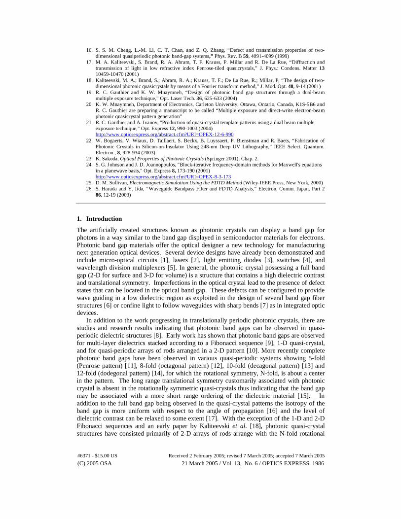
using a threshold exposure level of 12, 15, 9 and 13.5 for the 12-fold quasi-crystal. Due to the orientation of the planes, a threshold level set at 6 or lower results in the entire photoresist surface being fully exposed. The structures conventionally used to study quasi-crystal patterns are usually formed from a rotationally symmetric array of rods. The patterns of Fig. 1 demonstrate that the dielectric regions vary from isolated cylinders, ellipses, elongated tear drops, and rings with the fill factor (threshold level) determining the weight and connectivity of the dielectric islands. The quasi-crystal 12-fold pattern is generated with decreasing fill factor up to the threshold of 24 where the photoresist remains unexposed. A plot of the fill factor obtained versus threshold level (Curve A) and the change in fill factor versus a change of 0.5 in the threshold level (Curve B) is shown in Fig. 2. Curve A shows that a threshold set below 6 results in full exposure while a threshold above 6 results in a partially filled dielectric. Note the asymmetry in the filling versus threshold value in this figure. There is an abrupt drop in the fill factor at the onset of pattern definition that slowly trails off as the threshold approaches the maximum. The figure displays that a higher resolution in fill factor control is possible for low fill levels when a positive type photoresist is employed. A high sensitivity in the control of the fill factor for high dielectric fill factors is possible by reversing the polarity of the photoresist. Thus, depending on the polarity of the photoresist employed a high degree of control over the entire fill factor range is possible using the dual beam multiple exposure technique to generate the photonic crystal patterns. Details concerning how Figs. 1 and 2 were calculated can be found in a previous paper [19].
Fig. 1. 12-fold quasi-crystal patterns produced using different threshold levels for exposure. Dark regions correspond to unexposed resist and thus the high dielectric. (a) Threshold of 12 out of a maximum of 24 produces 50 % fill. (b) 9/24 giving 80% fill. (c) 15/24 giving 20 % fill. (d) 13.5/24 giving 33.3% fill.
3. Computation details
Frequency and time domain analysis are the primary techniques used to simulate and obtain the band properties of photonic crystals. For periodic crystals containing translational symmetry the plane wave expansion analysis in the frequency domain produces the band structure of sufficient accuracy and in a reasonable computational time. When the cell size is
(C) 2005 OSA 21 March 2005 / Vol. 13, No. 6 / OPTICS EXPRESS 1988#6371 - $15.00 US Received 2 February 2005; revised 7 March 2005; accepted 7 March 2005
increased, as is required to study defects, the computational domain increases as the square of the cell area, an order N3 process [23], and the computational time and memory requirement become very large. Techniques have been reported to increase the efficiency of a planewave techniques [24] to an N log N process. Given the larger computational time and repeated nature of the super-cell, reasonably accurate band and defect information can be obtained. However, these analyses are for circular dielectric rods arranged in a quasi-periodic array in the unit cell that repeats to generate the entire surface pattern. The photonic quasi-crystals examined here are non-periodic in the translational direction thus the identification of a super-cell is impractical from a computational point of view. Instead, the FDTD technique is employed to obtain transmission information as a function of propagation direction, wavelength and polarization.
Fig. 2. Curve A plots the high dielectric fill factor versus exposure threshold level used in the production of 12-fold quasi-crystal patterns. Curve B shows the change in the fill factor versus a threshold change of 0.5 . Curve C shows the reverse sensitivity regions and is obtained by inverting the polarity of the photoresist.
Data collection and processing enables the band information for the rotationally symmetric
quasi-crystals to be obtained. The photonic quasi-crystal patterns produced through the dual beam multiple exposure holographic lithography technique are discretized in a 100 by 100 grid per square micron of computational surface. The wavelengths examined in the analysis range from 0.9 µm to 1.8 µm in 0.01 µm increments.
The discretization grid provides a minimum of 99 grid points per free space wavelength at the shortest wavelength and 198 grid points at the longest wavelength. FDTD analysis is an order N process thus large grid areas can be discretized and analyzed in a reasonable computational time and memory requirement. The data obtained (E and H) over the grid is passed to a Fourier transform algorithm in order to extract transmission versus wavelength, propagation direction and polarization curves (i.e., TM or TE) for the quasi-crystal patterns of interest. Examination of the E field data over the quasi-crystal grid and its evolution as a function of time tends to indicate that the normal modes of the structure are composed of circularly symmetric functions which extend outwards from the center of the pattern. Although an inadequate theory exists for the modeling of the band gaps observed for quasi-crystal, the FDTD observations indicate that the expansion of the fields into a basis of circularly symmetric orthogonal functions may be suitable. Then the approach similar to that of the plane wave expansion with eigenvectors and eigenvalues may be applied with this new basis.
(C) 2005 OSA 21 March 2005 / Vol. 13, No. 6 / OPTICS EXPRESS 1989#6371 - $15.00 US Received 2 February 2005; revised 7 March 2005; accepted 7 March 2005
The FDTD algorithm that we employ is one available by Sullivan [25] and rewritten in a graphic display friendly language of Visual Basic. A PML is placed about the outside perimeter of the grid and extends for 15 grid points. The polarization of the incident plane wave is selected as either TM polarization with the Ez component in the extended direction of the dielectric, Hx and Hy components in the plane of the quasi-crystal pattern, or, TE polarization with the Hz component in the extended direction of the dielectric, Ex and Ey components in the plane of the quasi-crystal pattern. For the computations a plane wave soft source is employed with each wavelength contributing unit amplitude at the source grid points. In the FDTD computations the refractive index is treated as a constants with respect to wavelength range chosen even though the refractive index decreases with increasing wavelength. If required the effect of a non-constant refractive index can be inferred from the family of transmission figure presented as a function of dielectric contrast.
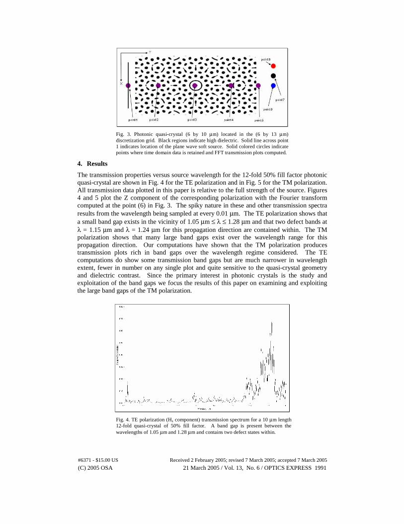
The transmission properties of the quasi-crystal structures are extracted using two different grid configurations. The first shown in Fig. 3 consists of a 6 by 13 µm (X down, Y across) surface. It can be shown that the features (i.e., location and size) of the PBG belonging to the photonic quasicrystal are the same for a square or rectangular domain. The only requirement when dealing with a rectangular domain is that some order of rotational symmetry needs to be retained. This is why 6 µm for the width was chosen. In this paper a rectangular domain is used to reduce the computational effort involved in analyzing waveguiding abilities of photonic quasicrystals. The quasi-crystal pattern extends the full X direction and from Y = 1 to Y = 11 µm with the center of the pattern at Y = 6 µm. The high dielectric regions of the structure are shown in black. The plane source extends from X = 1 to X = 5 µm (Y = 0.25) on the left side of the quasi-crystal structure. The 8 large circles are the points at which the Fourier transform data is extracted. These points provide the means of examining how the fields vary across the structure and at three points to the right of the structure after the fields have traversed the quasi-crystal. The transmission versus wavelength information is obtained by recording the various field values at all 8 points as function of time. The Fourier transform of this data into the frequency then wavelength domain ( ωπλ c2= ) gives the required information. For accurate transform curves to be produced in the order of 100,000 time domain points are required [26] per computational configuration. The second grid configuration consists of extending the Y-axis domain of Fig. 3 out to 40 µm. Once a steady oscillatory state of the fields on the output side of the quasi-crystal is obtained the spatial domain from Y = 13 to 39 µm is recorded and transformed to the wavelength domain using Fourier transform techniques. This second technique requires fewer computational domain points to return accurate information on the transmission properties of the quasi-crystal. However the computation time is comparable to the first technique due to the larger grid space. Results are presented using the smaller of the two computational grid domains. Results using the second technique are not presented as they were used to verify and support findings of the first technique. The computation algorithm and processing routines were verified by computing the transmission properties of well-known translationally period photonic crystals. It is found that the high wavelength regime of the transmission plots accurately reproduces the band gap regions while the low wavelength regime may be shifted by as much as 0.03 µm towards the low side. This shifting has to do with the nature of the FDTD technique and grid discretization size. It is well known that the FDTD technique introduces phase error as the number of grid points per wavelength is reduced [25]. Reasonably accurate results are expected when the grid sampling density is at or above 10 points per free space wavelength.
(C) 2005 OSA 21 March 2005 / Vol. 13, No. 6 / OPTICS EXPRESS 1990#6371 - $15.00 US Received 2 February 2005; revised 7 March 2005; accepted 7 March 2005
Fig. 3. Photonic quasi-crystal (6 by 10 µm) located in the (6 by 13 µm) discretization grid. Black regions indicate high dielectric. Solid line across point 1 indicates location of the plane wave soft source. Solid colored circles indicate points where time domain data is retained and FFT transmission plots computed.
4. Results
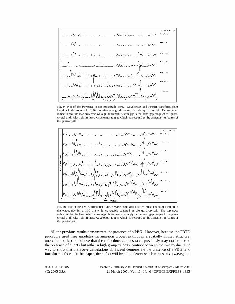
The transmission properties versus source wavelength for the 12-fold 50% fill factor photonic quasi-crystal are shown in Fig. 4 for the TE polarization and in Fig. 5 for the TM polarization. All transmission data plotted in this paper is relative to the full strength of the source. Figures 4 and 5 plot the Z component of the corresponding polarization with the Fourier transform computed at the point (6) in Fig. 3. The spiky nature in these and other transmission spectra results from the wavelength being sampled at every 0.01 µm. The TE polarization shows that a small band gap exists in the vicinity of 1.05 µm ≤ λ ≤ 1.28 µm and that two defect bands at λ = 1.15 µm and λ = 1.24 µm for this propagation direction are contained within. The TM polarization shows that many large band gaps exist over the wavelength range for this propagation direction. Our computations have shown that the TM polarization produces transmission plots rich in band gaps over the wavelength regime considered. The TE computations do show some transmission band gaps but are much narrower in wavelength extent, fewer in number on any single plot and quite sensitive to the quasi-crystal geometry and dielectric contrast. Since the primary interest in photonic crystals is the study and exploitation of the band gaps we focus the results of this paper on examining and exploiting the large band gaps of the TM polarization.
Fig. 4. TE polarization (Hz component) transmission spectrum for a 10 µm length 12-fold quasi-crystal of 50% fill factor. A band gap is present between the wavelengths of 1.05 µm and 1.28 µm and contains two defect states within.
(C) 2005 OSA 21 March 2005 / Vol. 13, No. 6 / OPTICS EXPRESS 1991#6371 - $15.00 US Received 2 February 2005; revised 7 March 2005; accepted 7 March 2005
Fig. 5. TM polarization (Ez component) transmission spectrum for a 10 µm length 12-fold quasi-crystal of 50% fill factor. Several band gap regions are present over the wavelength range displayed. Due to the rich nature of the band gaps for the TM polarization we explore in detail the optical properties of the 12-fold quasi-crystal for this polarization state of light.
Figure 6 shows a 3-D plot of the band structure versus wavelength and fill factor when the
source plane is normal incident to the quasi-crystal structure. Two dominant band gap regions are easily identified. The largest gap is centered about the 1.5 to 1.8 µm wavelength regime and the second is centered about the 1.0 µm wavelength regime. In the remainder of the paper we have examined the band gap properties of the 20% fill factor 12-fold quasi-crystal structure. The reason why 20% fill factor was chosen is because from Fig. 6, the photonic band gap is largest. The Ez field versus wavelength for the 20% fill factor structure versus wavelength is shown in Fig. 7 for various propagation angles. Because of the 12-fold rotational symmetry of the structure the transmission properties need only be examined over the 0 to 15 degree range. Propagation angles outside this range can be returned to an equivalent propagation angle inside the 15-degree range. The propagation angle curves are obtained by rotating the structure of the photonic quasi-crystal inside the rectangular grid of Fig. 3. The source remains the same in each plot and the propagation direction is normal to the photonic crystal entrance surface. As seen in this plot the band locations versus wavelength are quite insensitive to the propagation angle that results from the high degree of rotational symmetry for the 12-fold quasi-crystal structure. It should be possible to exploit the rotational isotropy in building waveguide devices with these 12-fold quasi-crystal structures.
(C) 2005 OSA 21 March 2005 / Vol. 13, No. 6 / OPTICS EXPRESS 1992#6371 - $15.00 US Received 2 February 2005; revised 7 March 2005; accepted 7 March 2005
Fig. 6. Line plot of the transmission spectrum for the Ez component of the TM polarization plotted versus wavelength and dielectric fill factor. The larger of the band gaps is located in the flat zone about the 1.5 µm wavelength value. A second large band gap is located in the 1.0 µm wavelength range.
Fig. 7. Line plot of the transmission spectrum for the Ez component of the TM polarization plotted versus wavelength and 0o to 15o propagation angle in 2.5o increments. Through rotational symmetry, other propagation angle outside 15o range can be rotated into the 0-15o range displayed. The quasi-crystal displays a uniform transmission spectrum over propagation angle.
Figure 8 shows a graph of the high wavelength band gap for the 12-fold quasi-crystal
versus dielectric contrast from 13:1 to 2:1. As expected the band is largest for the high dielectric end of the plot. If the idea is to design a device with a band gap in the 1.55 µm wavelength range (solid line through the band map), a high degree of tolerance is available in the selection of the dielectric contrast, Fig. 8, and fill factor, Fig. 6. Waveguides can be introduced in many different ways such as the rectangular guide produced by masking out a segment of the photonic crystal or by loading the dielectric medium in a periodic linear array of islands. The introduced waveguides may have any orientation with respect to the crystal structure. Because of the non-translational symmetry of the quasi-crystal pattern the location of the waveguide with respect to the central region (dot and ring of Fig. 3) is an important design feature. This implies that given the shape, orientation and dielectric value of the waveguide, its placement within the quasi-crystal structure can influence the optical guiding properties of the waveguide. This is a feature, not available in conventional photonic crystal arrangements, can be exploited by a careful and
(C) 2005 OSA 21 March 2005 / Vol. 13, No. 6 / OPTICS EXPRESS 1993#6371 - $15.00 US Received 2 February 2005; revised 7 March 2005; accepted 7 March 2005
skillful optical engineer. Straight rectangular waveguides where introduced into the photonic quasi-crystal of Fig. 3. The waveguides were chosen to have a relative dielectric value of 1, the background value, extend the full width (left to right) of the quasi-crystal, were centered on the quasi-crystal center, and have a waveguide width ranging from 0.25 µm to 1.5 µm. In order to better model the properties of the waveguides the crystal and waveguide were extended to 18 µm and the discretization grid extended to 6 µm by 20 µm. For any waveguide the source extent was made to equal the waveguide width and centered onto the waveguide. The continuous multi-wavelength source was propagated through the structure grid and the field values recorded at several locations along the waveguide and on waveguide output. This provides the means of examining the field transmission and attenuation versus propagation distance down the waveguide.
Fig. 8. High band gap region plotted versus dielectric fill factor. This large band gap exists down to a dielectric contrast of 2:1 but is considerably narrower than for high dielectric contrasts. The information displayed in Figs. 6-8 indicates that the design of a band gap in the 1.55 um range can be achieved through a large selection in the fill factor, dielectric contrast and propagation angle.
A typical plot of the Poynting vector magnitude and Ez field component versus wavelength
and position is shown in Fig. 9 and 10 respectively for the 1.50 µm wide waveguide. The wavelength range extending from 1.4 µm to 1.8 µm shows a high transmission in the waveguide. This same range corresponds to the large band gap of Figs. 6-8. The light in the low dielectric waveguide is confined to the waveguide, as it cannot propagate in the photonic quasi-crystal. In the range of 1.2 to 1.4 µm the waveguide transmission is low and results from the light in this wavelength range bleeding into the photonic quasi-crystal. The wave guiding properties in the 1.4 to 2.2 µm range is examined further by plotting field plots of the propagations and introducing waveguides of various geometry.
(C) 2005 OSA 21 March 2005 / Vol. 13, No. 6 / OPTICS EXPRESS 1994#6371 - $15.00 US Received 2 February 2005; revised 7 March 2005; accepted 7 March 2005
Fig. 9. Plot of the Poynting vector magnitude versus wavelength and Fourier transform point location in the center of a 1.50 µm wide waveguide centered on the quasi-crystal. The top trace indicates that the low dielectric waveguide transmits strongly in the band gap range of the quasi-crystal and leaks light in those wavelength ranges which correspond to the transmission bands of the quasi-crystal.
Fig. 10. Plot of the TM Ez component versus wavelength and Fourier transform point location in the waveguide for a 1.50 µm wide waveguide centered on the quasi-crystal. The top trace indicates that the low dielectric waveguide transmits strongly in the band gap range of the quasi-crystal and leaks light in those wavelength ranges which correspond to the transmission bands of the quasi-crystal.
All the previous results demonstrate the presence of a PBG. However, because the FDTD
procedure used here simulates transmission properties through a spatially limited structure, one could be lead to believe that the reflections demonstrated previously may not be due to the presence of a PBG but rather a high group velocity contrast between the two media. One way to show that the above calculations do indeed demonstrate the presence of a PBG is to introduce defects. In this paper, the defect will be a line defect which represents a waveguide
(C) 2005 OSA 21 March 2005 / Vol. 13, No. 6 / OPTICS EXPRESS 1995#6371 - $15.00 US Received 2 February 2005; revised 7 March 2005; accepted 7 March 2005
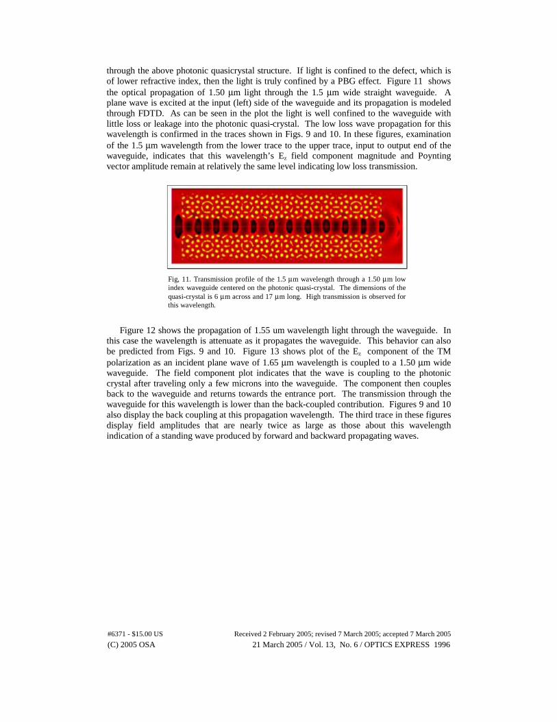
through the above photonic quasicrystal structure. If light is confined to the defect, which is of lower refractive index, then the light is truly confined by a PBG effect. Figure 11 shows the optical propagation of 1.50 µm light through the 1.5 µm wide straight waveguide. A plane wave is excited at the input (left) side of the waveguide and its propagation is modeled through FDTD. As can be seen in the plot the light is well confined to the waveguide with little loss or leakage into the photonic quasi-crystal. The low loss wave propagation for this wavelength is confirmed in the traces shown in Figs. 9 and 10. In these figures, examination of the 1.5 µm wavelength from the lower trace to the upper trace, input to output end of the waveguide, indicates that this wavelength’s Ez field component magnitude and Poynting vector amplitude remain at relatively the same level indicating low loss transmission.
Fig, 11. Transmission profile of the 1.5 µm wavelength through a 1.50 µm low index waveguide centered on the photonic quasi-crystal. The dimensions of the quasi-crystal is 6 µm across and 17 µm long. High transmission is observed for this wavelength.
Figure 12 shows the propagation of 1.55 um wavelength light through the waveguide. In
this case the wavelength is attenuate as it propagates the waveguide. This behavior can also be predicted from Figs. 9 and 10. Figure 13 shows plot of the Ez component of the TM polarization as an incident plane wave of 1.65 µm wavelength is coupled to a 1.50 µm wide waveguide. The field component plot indicates that the wave is coupling to the photonic crystal after traveling only a few microns into the waveguide. The component then couples back to the waveguide and returns towards the entrance port. The transmission through the waveguide for this wavelength is lower than the back-coupled contribution. Figures 9 and 10 also display the back coupling at this propagation wavelength. The third trace in these figures display field amplitudes that are nearly twice as large as those about this wavelength indication of a standing wave produced by forward and backward propagating waves.
(C) 2005 OSA 21 March 2005 / Vol. 13, No. 6 / OPTICS EXPRESS 1996#6371 - $15.00 US Received 2 February 2005; revised 7 March 2005; accepted 7 March 2005
Fig. 12. Transmission profile (b) of the 1.55 µm wavelength through a 1.50 µm low index waveguide centered on the photonic quasi-crystal (a). The dimensions of the quasi-crystal structure is 6 µm across and 17 µm long. The waveguide transmits an attenuated light for this particular wavelength.
Fig. 13. Transmission profile (b) of the 1.65 µm wavelength through a 1.50 µm low index waveguide centered on the photonic quasi-crystal (a). The dimensions of the quasi-crystal is 6 µm across and 17 µm long. The waveguide displays a resonant back coupling of the light with only a small transmitted contribution.
Figure 14 demonstrates that photonic quasicrystals can also be used as Y-splitters. The
input consists of 1.50 µm wavelength on the left side and is propagated to the center of the photonic quasi-crystal. At the Y split the power is divided between the two branches and propagates to the exit ports on the right. There is also a back-reflected component at the Y split that returns along the input waveguide path. This simulation was essentially a proof-of-concept design and was in no way optimized.
(C) 2005 OSA 21 March 2005 / Vol. 13, No. 6 / OPTICS EXPRESS 1997#6371 - $15.00 US Received 2 February 2005; revised 7 March 2005; accepted 7 March 2005
Fig. 14. Transmission profile of the 1.50 µm wavelength through a Y splitter fabricated from low index 1.50 µm waveguides positioned in the photonic quasi-crystal. Quasi-crystal 6 µm across and 17 µm long. The splitter divides the power and excites the two output ports evenly. The Y junction also generates a small backwards propagating component which exits the input waveguide. No attempts were made to optimize the Y branches splitting properties.
5. Conclusions
We have shown the optical guiding and transmission properties of TM polarized in the 2-D 12-fold planar quasi-crystal structure. The patterns examined based on fill-factor and dielectric contrast can be easily written using optical holographic lithography or conventional e-beam techniques. Our results obtained through FDTD analysis indicate that the TM polarization is rich in band gap and defect properties. Several interesting waveguide properties are presented and include a propagation that is relatively angle independent but is placement dependent relative to the center of the quasi-crystal pattern. The optical and waveguide properties of the 12-fold quasi-crystal indicate that new and interesting devices designs may be designed.
(C) 2005 OSA 21 March 2005 / Vol. 13, No. 6 / OPTICS EXPRESS 1998#6371 - $15.00 US Received 2 February 2005; revised 7 March 2005; accepted 7 March 2005