Photonic crystal microcavity engineering and high-density bio-patterning for chip-integrated microarray applications
Swapnajit Chakravarty*a, Wei-Cheng Laib, Yi Zoub, Ray T. Chenb, aOmega Optics Inc., 10306 Sausalito Drive, Austin, TX, USA 78759; bDept. of Electrical and Computer Engineering, University of Texas, 10100 Burnet Road Bldg. 160, Austin, TX, USA
78758;
ABSTRACT
While Q ~ 1million has been demonstrated in freely suspended photonic crystal (PC) membranes, the reduced refractive index contrast when PC microcavities are immersed in phosphate buffered saline (PBS), a typical ambient for biomolecules, reduces Q by more than 2 orders of magnitude. We experimentally demonstrate photonic crystal microcavity based resonant sensors coupled to photonic crystal waveguides in silicon on insulator for chemical and bio-sensing. Linear L-type microcavities are considered. In contrast to cavities with small modes volumes but low quality factors for bio-sensing, we show that increasing the length of the microcavity enhances the quality factor of the resonance by an order of magnitude and also increases the resonance wavelength shift while still retaining compact device characteristics. Q~26,760 and sensitivity down to 7.5ng/ml and ~9pg/mm2 in bio-sensing was experimentally demonstrated in SOI devices for goat anti-rabbit IgG antibodies with Kd~10-6M. The increase in cavity length follows from fundamental engineering limitations in ink-jet printing or microfluidic channels when unique receptor biomolecules are coated on separate adjacent sensors in a microarray.
1. INTRODUCTION Integrated optical devices are being developed in recent years to function as microarrays for chemical and biological assays. Platforms based on ring resonators [1], wire waveguides [2] and surface plasmon resonance (SPR) [3] have been investigated. The detection principle in all instances with the different platforms is based on the specific binding of the biomolecule of interest to its specific conjugate biomolecule receptor bound to the optical device substrate, which causes a change in the refractive index and hence a change in the transduced signal. It is possible to design sensors with ultra-small mode volumes [4], however, current bio-molecule patterning technologies limit the minimum spacing between resonators in an array when each sensor is coated with a unique biomolecule receptor. There are two methods used primarily for bio-patterning: ink-jet printing and microfluidic channels. Ink-jet printing techniques [5] enable denser integration than methods using microfluidic channels where laminar flow considerations make miniaturization challenging below 100μm for effective biomolecule patterning [2]. Over the last decade, photonic crystals (PCs) have generated significant interest due to their ability to confine light to ultra-small mode volumes and their high sensitivity to changes in refractive index of the ambient that promises the potential for creating high-density microarrays. Various designs of PCs have been proposed for chemical [6] and bio-sensing [7] using waveguides [8-9] and microcavities [10] with small mode volumes. However, as the refractive index of the ambient increases, radiation losses increase that significantly reduces the resonance quality (Q) factor due to reduced out-of-plane confinement in two-dimensional PCs. Hence although high Q-factors have been demonstrated in freely suspended PC membranes in air [11], when such membranes are suspended in phosphate buffered saline (PBS) (refractive index n = 1.334), a typical ambient for bio-molecules, Q-factors deteriorate by orders of magnitude. Hence designs for nanophotonic biosensors on the photonic crystal platform have attempted to balance two contradictory requirements: increasing the Q-factor of the resonance versus increasing the wavelength shift due to change in refractive index. In passive silicon PC nanostructures, the transmission drop-resonance architecture has been used predominantly with hexagonal [7] and linear PC microcavity [10-11] coupled to a W1 photonic crystal waveguide (PCW). The best
Frontiers in Biological Detection: From Nanosensors to Systems IV, edited by Benjamin L. Miller, Philippe M. Fauchet, Proc. of SPIE Vol. 8212, 82120A
Downloaded from SPIE Digital Library on 25 May 2012 to 206.76.84.74. Terms of Use: http://spiedl.org/terms
results have been achieved in freely suspended membranes [11]. Freely suspended membranes are however very fragile due to the absence of supporting material beneath, and hence pose challenges for use in harsh environments and perhaps even for everyday rough use in a diagnostic assay chip for medical applications. Furthermore, it is generally accepted that the yield of free-standing photonic crystal membranes is usually very low. In this paper, we present high-Q PC microcavities in silicon on insulator structures for bio-sensing microarray applications. The use of silicon-on-insulator ensures the fabrication of robust devices with high yield. Furthermore, since radiation losses are inversely proportional to the cavity size [4] and due to fundamental biomolecule patterning limitations in microarrays, we investigate methods to increase device sensitivity by increasing the size of the PC microcavity while still retaining the compactness of PC structures.
2. DEVICE DESIGN The photonic crystal waveguide (PCW) is a hexagonal structure with a W1 line defect waveguide with uniform lattice constant a=400nm, where W1 denotes that width of the PCW is √3a. Silicon slab thickness and air hole diameter are h=0.58a and d=0.54a as shown in Fig. 1(a).A microscope image of a patterned device with an array of two PC microcavities is shown in Fig. 1(b). Detailed characteristics of the arrayed device will be covered in another publication. In this paper, we consider single PC microcavity sensors only. In Fig. 1(b), we note that by ink-jet patterning, the minimum dispensed spot size of biomolecules is ~35μm. The biomolecules were mixed with glycerol prior to ink-jet dispensing to avoid folding of the proteins that would clog the nozzles of the ink-jet printer. It may be noted here that it has been demonstrated that by combining lithographic patterning with ink-jet printing, it is possible to shrink the printed area down to sub-μm2 area. However, when two different biomolecules need to be dispensed in a microarray, the ink-jet dispensed spot size determines the minimum spacing between adjacent sensors, and not the device surface area that can be functionalized by combining lithographic patterning with ink-jet printing [5]. PC microcavities of gradually increasing length were thus investigated to characterize resonance line-widths and sensitivity. Linear PC microcavities Ln where n presents the number of missing holes along Γ−Κ direction, are fabricated two periods away from the PCW. The edge air holes are shifted in the Γ−Κ direction by 0.15a [4]. Fig. 1(c) shows a band structure obtained by three-dimensional plane-wave expansion simulations of the W1 PCW, considering water (n=1.33) as the ambient. The normalized resonance frequencies of different PC microcavities of increasing lengths obtained by 3D finite-difference time domain simulations are indicated by dotted lines in Fig. 1(c). The resonant mode profiles are shown in the insets.
Fig. 1. (a) Device schematic (b) Ink-jet printed biomolecules on PC devices showing spacing between printed spots (scale bar is 10μm) (c) Dispersion diagram of W1 PCW in water. The W1 guided mode is shown together with frequencies of resonant modes for L3, L7 and L13 PC microcavities by dashed lines. Respective mode profiles are shown in insets.
3. EXPERIMENTAL SETUP The devices were tested on a Newport six-axis auto-aligning station. Input light from a broadband source was TE-polarized and butt-coupled to / from the device with polarization maintaining single mode tapered lensed fiber with
Proc. of SPIE Vol. 8212 82120A-2
Downloaded from SPIE Digital Library on 25 May 2012 to 206.76.84.74. Terms of Use: http://spiedl.org/terms
mode field diameter ~3μm. Light is guided in and out of the PCW by ridge waveguides with PC group index taper to enable high coupling efficiency into the slow light guided mode [12]. Devices were fabricated on silicon-on-insulator (SOI) wafer using established methods [12]. The transmission drop resonance Q and sensitivity to bulk refractive index changes are analyzed with water and isopropyl alcohol (IPA) (n=1.377) as the ambient medium.
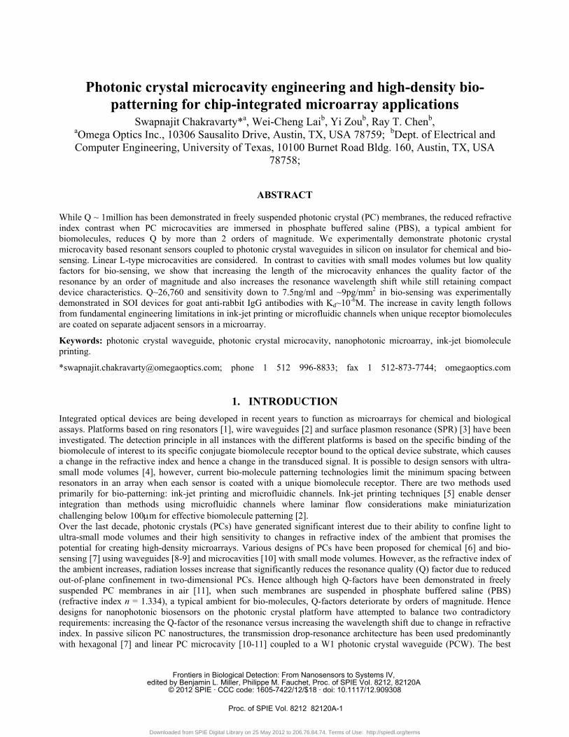
4. EXPERIMENTAL RESULTS Figs. 2 (a)-(c) show experimental transmission spectra from W1 PCWs with coupled L3, L7 and L13 PC microcavities in water. In Figs. 2 (d)-(f), drop transmission of the resonance closest to the band edge, as in insets of Fig. 1(c), for L3, L7 and L13 PC microcavities in water and IPA are shown.
Fig. 2. Experimental W1 PCW transmission spectrum in water with coupled (a) L3 (b) L7 and (c) L13 microcavities. Experimental spectra showing shift of resonance mode closest to the band edge in (a), (b) and (c) in (d), (e) and (f) respectively in water (black) versus IPA (blue). (inset (e)) magnifies the wavelength range.
Fig. 3. Plots showing trends in L3, L7 and L13 PC microcavities for resonant mode (a) quality factor in water (open circle) (b) quality factor in IPA (open square) (c) approximate mode offset from the transmission band edge (filled square, left offset axis) and (d) wavelength shift from water to IPA (filled triangle, left axis).
Proc. of SPIE Vol. 8212 82120A-3
Downloaded from SPIE Digital Library on 25 May 2012 to 206.76.84.74. Terms of Use: http://spiedl.org/terms
Fig. 3 shows resonance shifts Δλ observed experimentally with the device in water versus in IPA. Fig. 3 also plots experimental Q (=λ/Δλ) in water and IPA, at the center frequency, and the approximate resonance offset ΔΛ from the W1 transmission band edge. It is observed from Fig. 3 that as the resonance moves closer to the band edge of the W1 PCW, Q and Δλ increase. Since IPA does not absorb in the wavelength range studied, Q in IPA is higher than in water. The increase in Q as the resonance approaches increasing group index near the band edge, is due to the combined effect of cold cavity Q, due to the inverse dependence of radiation loss on cavity size, and the diverging waveguide density of states [13] in the coupled cavity-waveguide system as the resonance moves deeper into the photonic band gap. Due to increase in mode volume, the resonance mode overlaps with more air holes along the borders of the cavity, leading to higher Δλ. By microcavity engineering, the highest Q~26760 was observed in a L13 PC microcavity in a SOI device with sensitivity S ~52nm/RIU (RIU=refractive index unit). S is calculated as S=Δλ/Δn from values in water and IPA. Similar sensitivities were achieved in single-period resonators in SOI with Q ~450 [14]. The high Q in our device improves measurement resolution for the detection of smaller changes in concentration.
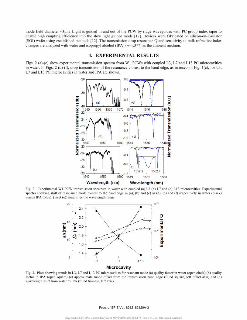
5. DEVICE DESIGN FOR BIOSENSING The device parameters are the same as in Fig. 1. Simulations are performed considering phosphate buffered saline (PBS) (n=1.334) as the ambient and hence forms the top cladding and the material filling the photonic crystal air holes. The frequency of the resonance mode is indicated by the black dashed line in the dispersion diagram of the W1 PCW by three dimensional plane-wave expansion (PWE) in Fig. 4(a). The dispersion diagram of the W1 PCW is shown by the solid black curves. At the resonance frequency, prior to coupling to the PC microcavity, light propagates through the PCW with a group velocity slower than its velocity in the input ridge waveguide. To lower the effect of Fresnel reflection due to the group index mismatch between the ridge waveguide and the PCW, a gradual group index taper is needed from the ridge waveguide to the PCW. The gradual change in group velocity is achieved by gradually increasing the radius of holes adjacent to the PCW as shown in the SEM image in Fig. 4(b). At the entrance of the PCW, the diameter d1 of the holes is 0.8775× 0.54a. The dispersion diagram of the W1 PCW with d1=0.8775× 0.54a is indicated by the solid blue curves. As observed from the band structure simulation in Fig. 2(a), this band engineering has the effect of gradually decreasing group velocity vg=δω/δk from the PCW-ridge waveguide entrance to the slow light PCW guiding frequency of the resonant mode as indicated by the slope of the red dashed lines. The choice of d1 is made to ensure that higher order modes do not overlap with the W1 guided mode with d=0.54a as indicated by the black dashed arrow. It has been shown previously [12] that such band engineering improves the coupling efficiency at slow light wavelengths.
(a) (b)
Fig. 4: (a) Dispersion diagram of W1 photonic crystal waveguide for d=0.54a (black curves) and d=0.8775×0.54a (blue curves). The resonance frequency of L13 PC microcavity is shown by black dashed line. The group velocity at the coupling frequency is indicated by the dashed red line. The W1 guided modes are indicated by the black and blue arrows. The black dotted line indicates the upper bound of the radius taper design as determined by the frequency of the higher order mode. (b) SEM image of the input of the photonic crystal waveguide from the ridge waveguide indicating the group index taper.
Proc. of SPIE Vol. 8212 82120A-4
Downloaded from SPIE Digital Library on 25 May 2012 to 206.76.84.74. Terms of Use: http://spiedl.org/terms
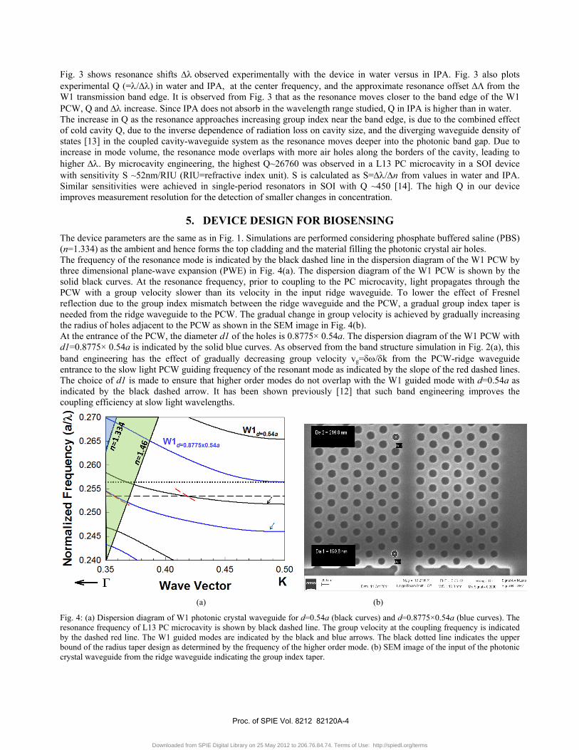
6. BIOSENSING RESULTS The enhanced sensitivity and resolution is next applied to bio-sensing. Wafers were functionalized by treating with 3-aminoprpyl-triethoxy-silane (3-APTES) in water, followed by washing 3 times in PBS. Wafers are next incubated in 1% glutaraldehyde in PBS for 5 minutes, ink-jet printed with target antibodies (Abs) and washed 3 times in PBS. 60μl of probe Antibody was directly dispensed from a micro-pipette. The diameter of the dispensed spot on silicon is ~8mm.
Fig. 5. (a) Resonance wavelength of L3 PC microcavity at different steps in the binding sequence. The resonant wavelength shift of interest is denoted by Δλ. (b) Resonance shift of L3 (filled circles) and L13 PC microcavities (open circles) with probe antibody binding. Dashed line indicates the detection limit.
After each new concentration of probe antibody, the devices are washed in PBS and the resonance wavelength measured. While surface binding of target antibody can also be used to characterize device sensitivity, the resonance wavelength shift of interest for such hybrid assays is shown by Δλ in Fig. 5(a) which measures the probe antigen containing the predefined spectral response that is specifically bound to the target antibody. In Fig. 5(b), the magnitude of resonance shift as a function of rabbit anti-goat binding to goat anti-rabbit (molecular weight MW=150kDa) antibodies is plotted for L3 and L13 microcavities respectively. As in chemical sensing, higher Q ~9,300 and larger sensitivity is observed for L13 than L3 PC microcavities. This represents the highest Q reported for bio-sensing in SOI PC devices. We experimentally detected binding of 0.1nM or 15ng/ml of probe antibody with L13 and L3 devices but a much larger wavelength shift (0.08nm) for L13 devices, as seen from Fig. 5(b). Since dn/dT=1.87×10-4 at 295K for silicon, if we consider a maximum variation of 1K in temperature, the biomolecule sensing measurement limit of the shift Δλ is 0.01nm from the measured bulk sensitivity. The wavelength accuracy of our optical spectrum analyzer is 0.02nm. Hence the measurement limit is indicated by the dashed line at 0.02nm. The extrapolated concentration detection limit with L13 devices is thus ~50pM for which we measured a resonance wavelength shift of 0.03nm. In Fig. 1(c) inset, with a sensing area ~11μm2, (integrating over an area where the E-field intensity is more than 50% of maximum value and including the internal surface area of holes along the periphery of the photonic crystal microcavity where the E-field is stronger than 50% over a fraction of the periphery of the PC microcavity) [15], dispensed probe antibody volume of 60μl over a diameter 8mm, and assuming uniform surface coverage, the estimated mass detection limit for goat anti-rabbit IgG antibodies with dissociation constant Kd ~10-6M, without considering unbound antibodies that are washed away, in L13 devices is ~98 atto-grams. The detection limit for surface density is ~9pg/mm2 which compares quite favorably with detection limits of 1pg/mm2 in SPR, on more than 4 orders of magnitude smaller area [3]. The detection limit also compares favorably with 60pg/mm2 estimated in ref. [16]. Experimentally, we detected 9pg/mm2 of bound antibody. Actual bound mass will be much lower since a significant fraction is washed away.
7. SUMMARY In summary, we demonstrated a method for bio-sensing coupling high quality factor resonance and high sensitivity in SOI PC devices. The wave-guiding nature of our device enables denser chip-scale miniaturization than SPR microarrays, and the ability to probe multiple devices simultaneously for high throughput measurements. Our method which increases
Proc. of SPIE Vol. 8212 82120A-5
Downloaded from SPIE Digital Library on 25 May 2012 to 206.76.84.74. Terms of Use: http://spiedl.org/terms
the size of the photonic crystal microcavity than ones usually studied is justified from practical limitations of bio-patterning using ink-jet printing or microfluidic channels which limit the minimum spacing that can be achieved between adjacent sensors that are coated with receptor biomolecules in a chip-integrated microarray.
ACKNOWLEDGEMENTS
The authors would like to acknowledge the National Cancer Institute for supporting this work under the Small Business Innovation Research (SBIR) program (HHSN261201000085C).
REFERENCES
[1] Iqbal, M., Gleeson, M.A., Spaugh, B., Tybor, F., Gunn, W.G., Hochberg, M., Baehr-Jones, T., Bailey, R.C., and Gunn, L.C., “Label-Free Biosensor Arrays based on silicon ring resonators and high-speed optical scanning instrumentation”, IEEE J. Sel. Top. Quant. Electron. 16(3), 654 (2010).
[2] Densmore, A., Vachon, M., Xu, D.X., Janz, S., Ma, R., Li, Y.H., Lopinski, G., Delage, A., Lapointe, J., Luebbert, C.C., Liu, Q.Y., Cheben, P., and Schmid, J.H., “Silicon photonic wire biosensor array for multiplexed real-time and label-free molecular detection”, Opt. Lett. 34(23), 3598 (2009).
[3] Sipova, H., Zhang, S., Dudley, A.M., Galas, D., Wang, K., and Homola, J., “Surface plasmon resonance biosensor for rapid label-free detection of microribonucleic acid at subfemtomole level”, Anal. Chem. 82, 10110 (2010).
[4] Akahane, Y., Asano, T., Song, B-S., and Noda, S., “High-Q photonic nanocavity in a two-dimensional photonic crystal”, Nature 425 (6961), 944 (2003).
[5] Tan, C.P., Cipriany, B.R., Lin, D.M., and Craighead, H.G., “Nanoscale resolution, multicomponent biomolecular arrays generated by aligned printing with parylene peel-off”, Nano Lett, 10, 719-725 (2010).
[7] Lee, M., and Fauchet, P.M., “Two-dimensional silicon photonic crystal based biosensing platform for protein detection”, Opt. Express 15, 4530-4535 (2007).
[8] Lai, W-C., Chakravarty, S., Wang, X., Lin, C., Chen, R.T., “On-Chip methane sensing by near-IR absorption signatures in a photonic crystal slot waveguide”, Optics Lett. 36 (6), 984 (2011).
[9] Lai, W-C., Chakravarty, S., Wang, X., Lin, C., Chen, R.T., “Photonic Crystal Slot Waveguide Absorption Spectrometer for On-Chip Near-Infrared Spectroscopy of Xylene in Water”, Appl. Phys. Lett. 98 (2), 023304 (2011).
[10] Lai, W-C., Chakravarty, S., Wang, X., Lin, C., Chen, R.T., “Silicon Nano-Membrane based Photonic Crystal Microcavities for High Sensitivity Bio-Sensing”, Optics Lett. (in review).
[11] Kang, C., Phare, C.T., Vlasov, Y.A., Assefa, S., and Weiss, S. M., “Photonic crystal slab sensor with enhanced surface area”, Opt. Express 18(26), 27930 (2010).
[12] Lin, C-Y., Wang, X., Chakravarty, S., Lee, B-S., Lai, W-C., and Chen, R.T., “Wideband Group Velocity Independent Coupling into Slow Light Silicon Photonic Crystal Waveguide,” Appl. Phys. Lett. 97 (18), 183302 (2010)
[13] Waks, E. and Vuckovic, J., “Coupled mode theory for photonic crystal cavity-waveguide interaction”, Opt. Express 13(13), 5064 (2005).
[14] Pal, S., Guillermain, E., Sriram, R., Miller, B.L., Fauchet, P.M., “Silicon photonic crystal nanocavity-coupled waveguides for error-corrected optical biosensing”, Biosens. and Bioelectron. 26, 4024 (2011).
[15] Scullion, M.G., Di Falco, A., and Krauss, T.F., “Slotted photonic crystal cavities with integrated microfluidics for biosensing applications”, Biosens. and Bioelectron. 27, 101 (2011).
[16] Dorfner, D., Zabel, T., Hurlimann, T., Hauke, N., Frandsen, L., Rant, U., Abstreiter, G., and Finley, J., “Photonic crystal nanostructures for optical biosensing applications”, Biosens. and Bioelectron. 24, 2688 (2009).
Proc. of SPIE Vol. 8212 82120A-6
Downloaded from SPIE Digital Library on 25 May 2012 to 206.76.84.74. Terms of Use: http://spiedl.org/terms