13 Photonic Crystals for Plasmonics: From Fundamentals to Superhydrophobic Devices Remo Proietti Zaccaria et al. * Nanobiotech Facility, Italian Institute of Technology, Genova Italy 1. Introduction In the last couple of decades we have been witnessing an enormous technological advancement in the field of micro-technology to the extent that nowadays we talk about nanotechnology. Faster computers, LCD based mobiles, nanoparticles for UV absorption in suntan lotions are just few of many examples where nanotechnology plays a fundamental role. The merit of this is mainly in the advance of the fabrication methods. Present techniques such as Focused Ion Beam (FIB) lithography guarantee a resolution of less than 10 nanometers which is about five times more precise than ten years before. Also Photonic Crystals (PhCs), among the others, take advantage from this extremely high resolution level allowing a downscale that permits the realization of structures which in principle can work at vey high energy. Historically PhCs were known as Bragg mirrors and only in 1987 (Yablonovitch, 1987; Sajeev, 1987) with the works of Yablonovitch and Sajeev the term Photonic Crystals was introduced. Nowadays, besides their natural application as filters in particular under full band gap conditions, PhCs see a number of applications: optical fibers (Birks et al., 1997; Zhao et al., 2010), vertical cavity surface emitting lasers (Yokouchi et al., 2003), high reflection coatings, temperature sensors (Song et al., 2006), high efficiency solar cells (Bermel et al., 2007), electric field detectors (Song & Proietti Zaccaria, 2007), non-linear analysis (Malvezzi et al., 2002; Malvezzi et al., 2003), just to name a few. Many are the techniques for the fabrication of PhCs, for example by means of focused-ion beam (Cabrini et al., 2005), two-photon fabrication (Deubel et al., 2004), laser-interference (Proietti Zaccaria et al., 2008a) or waver-fusion techniques (Takahashi et al., 2006). Here we shall focus on the role that PhCs can play for another exciting discipline known as Plasmonics. It refers to the capability of some devices of sustaining an optical surface mode, namely an electromagnetic wave travelling at the interface between two different materials such as a dielectric and a metal. Such a wave originates from the coupling of incident photons on the interface with * Anisha Gopalakrishnan 1 , Gobind Das 1 , Francesco Gentile 1,2 , Ali Haddadpour 3 , Andrea Toma 1 , Francesco De Angelis 1 , Carlo Liberale 1 , Federico Mecarini 1 , Luca Razzari 1 , Andrea Giugni 1 , Roman Krahne 1 and Enzo Di Fabrizio 1,2 1 Nanobiotech Facility, Italian Institute of Technology, Genova ,Italy 2 BIONEM lab., Departement of Clinical and Experimental Medicine, Magna Graecia University, viale Europa, Catanzaro, Italy 3 Department of Electrical and Computer Engineering, University of Tabriz, Iran www.intechopen.com
Transcript
13
Photonic Crystals for Plasmonics: From Fundamentals to Superhydrophobic Devices
Remo Proietti Zaccaria et al.* Nanobiotech Facility, Italian Institute of Technology, Genova
Italy
1. Introduction
In the last couple of decades we have been witnessing an enormous technological advancement in the field of micro-technology to the extent that nowadays we talk about nanotechnology. Faster computers, LCD based mobiles, nanoparticles for UV absorption in suntan lotions are just few of many examples where nanotechnology plays a fundamental role. The merit of this is mainly in the advance of the fabrication methods. Present techniques such as Focused Ion Beam (FIB) lithography guarantee a resolution of less than 10 nanometers which is about five times more precise than ten years before. Also Photonic Crystals (PhCs), among the others, take advantage from this extremely high resolution level allowing a downscale that permits the realization of structures which in principle can work at vey high energy. Historically PhCs were known as Bragg mirrors and only in 1987 (Yablonovitch, 1987; Sajeev, 1987) with the works of Yablonovitch and Sajeev the term Photonic Crystals was introduced. Nowadays, besides their natural application as filters in particular under full band gap conditions, PhCs see a number of applications: optical fibers (Birks et al., 1997; Zhao et al., 2010), vertical cavity surface emitting lasers (Yokouchi et al., 2003), high reflection coatings, temperature sensors (Song et al., 2006), high efficiency solar cells (Bermel et al., 2007), electric field detectors (Song & Proietti Zaccaria, 2007), non-linear analysis (Malvezzi et al., 2002; Malvezzi et al., 2003), just to name a few. Many are the techniques for the fabrication of PhCs, for example by means of focused-ion beam (Cabrini et al., 2005), two-photon fabrication (Deubel et al., 2004), laser-interference (Proietti Zaccaria et al., 2008a) or waver-fusion techniques (Takahashi et al., 2006). Here we shall focus on the role that PhCs can play for another exciting discipline known as Plasmonics. It refers to the capability of some devices of sustaining an optical surface mode, namely an electromagnetic wave travelling at the interface between two different materials such as a dielectric and a metal. Such a wave originates from the coupling of incident photons on the interface with
* Anisha Gopalakrishnan1, Gobind Das1, Francesco Gentile1,2, Ali Haddadpour3, Andrea Toma1, Francesco De Angelis1, Carlo Liberale1, Federico Mecarini1, Luca Razzari1, Andrea Giugni1, Roman Krahne1 and Enzo Di Fabrizio1,2
1Nanobiotech Facility, Italian Institute of Technology, Genova ,Italy 2BIONEM lab., Departement of Clinical and Experimental Medicine, Magna Graecia University, viale Europa, Catanzaro, Italy 3Department of Electrical and Computer Engineering, University of Tabriz, Iran
www.intechopen.com
Photonic Crystals – Innovative Systems, Lasers and Waveguides
258
the existing free electrons. This kind of mode is known as Surface Plasmon Polariton (SPP). Photonic crystals, as a translational modulation of the refractive index, have already been playing a very crucial role in plasmonics. In fact, they can provide the missing wave vector for the coupling between photons and free electrons of a metal layer (Raether, 1988). Here we have chosen to face three situations relating PhCs and Plasmonics:
a. two dimensional (2D) metallic photonic crystal for maximizing the optical band gap; b. metallic photonic crystal structures for Surface Enhanced Raman Spectroscopy (SERS); c. few molecules detection through super-hydrophobic crystals (De Angelis et al., 2011).
The first topic concerns the fundamentals of SPP and PhCs. No particular application will be suggested, but mostly we will focus on the theory behind the generation of SPP inside a metallic photonic crystal. The next two topics are, on the other hand, strictly related to applications. We will concentrate our attention on Raman spectroscopy, as a very important tool for the investigation of the optical properties of many kinds of samples, such as semiconductors or proteins. In particular, metallic ordered (periodic) structures will be used either as artificial SERS substrates or as combiners of SERS and super-hydrophobic effect for few molecules detection. This description will offer a general overview of the important functions that PhCs can hold in Plasmonics and how we could start thinking more intensively of PhCs realized with metallic materials.
2. Two dimensional metallic PhCs for maximum full band gap
One of the main issues when dealing with two dimensional PhCs is the maximum full band gap that the crystal can provide. Specifically, in 2D the crystal manifests two non degenerative polarizations known as TE and TM. The former refers to solutions with the electric field in the plane of symmetry of the crystal, the latter with the magnetic field in the same plane. In order to produce a full band gap, both TE and TM must provide an optical gap in the same spectral region. This is not an easy task and different solutions have been proposed (Joannopoulos et al., 1995), however mostly referring to dielectric PhCs. Here we shall examine how metallic PhCs can improve the chance of a common band gap between TE and TM with respect to a dielectric structure.
2.1 Dielectric photonic crystals
It has been demonstrated that the geometry of PhCs strongly affect whether TE or TM band gap will be generated. In particular, when the crystal is formed by isolated regions of high dielectric, the TM gap is favored; when the crystal is formed by connected regions of high dielectric, the TE gap is favored. Hence, the geometry plays a crucial role. In regards, when 2D photonic crystals are considered, only five possible geometrical arrangements exist. These are called Bravais lattices. Considering the complementary conditions for the realization of a TE/TM gaps, the best Bravais lattice to maximize the probability of obtaining a full band gap is the hexagonal one. This kind of Bravais lattice posses the highest possible rotational symmetry in two dimensions. In view of this information, we have instead chosen the square photonic crystal (Galli et al., 2002), namely a configuration not supporting a full band gap for isotropic dielectric materials (Wang et al., 2005; Proietti Zaccaria, 2008b). In this manner we expect to enhance the different results in terms of full band gap rising either from a dielectric crystal or a metallic one.
www.intechopen.com
Photonic Crystals for Plasmonics: From Fundamentals to Superhydrophobic Devices
259
2.1.1 Full band gap in dielectric 2D photonic crystals
The chosen dielectric PhC is made of circular columns of high refractive index material, namely silicon (n=3.6) surrounded by air (n=1). The radius of the columns is r=300nm and lattice period P=1m. As expected, only TM polarization shows zero transmission regions, in particular three band gaps below 1m-1 are shown in Fig. 2.1. On the other hand, TE does not sustain any band gap. These results remain true even increasing the columns dielectric value or changing the columns radius. No full band gap is then found for this kind of structure.
Fig. 2.1. TM band structure for a 2D square silicon columns photonic crystal. Three band gaps are shown.
2.2 Metallic photonic crystals
The behavior of 2D metallic photonic crystals is fundamentally different from what expected by 2D dielectric photonic crystals (Zhao et al., 2009; Sakoda et al., 2001; Ito & Sakoda, 2001). In fact, the use of metallic dispersive materials strongly modifies the light behavior in periodic structures, both for TM and TE polarizations. In particular, TM polarization shows a cut-off frequency c and no modes are found below it. This implies the existence of a TM gap below c. From a physical point of view this is related to the existence of free electrons in metallic materials. Similarly, TE polarization shows a behavior which is absent in dielectric 2D photonic crystals. In fact, in specific range of frequencies, metallic photonic crystals show TE polaritonic band gap close to the plasma frequency. Physically it is associated to the creation of surface plasmon polaritons on the metallic columns of the crystal. These peculiarities of metallic PhCs have the merit of increasing the chance of a full band gap also for square crystals. Hence, maintaining the same geometrical configuration as in the previous section, namely a square structure of columns in air, we have numerically analyzed the band gap formation when metallic columns are considered instead of dielectric ones.
2.2.1 Full band gap in metallic 2D photonic crystals: Drude vs. Lorentz model
We start by considering the Drude model (Rakic´ et al., 1998) to describe the metallic parts of the crystal:
2
02
0
( ) 1 pf
i
(2.1)
www.intechopen.com
Photonic Crystals – Innovative Systems, Lasers and Waveguides
260
where p is the plasma frequency, 0 is the damping constant and f0 is the oscillator strength. We recall that this model is a simplified version of the realistic Drude-Lorentz model, in fact it does not describe the material resonances (absorption) of the metal. Nevertheless, the Drude model is commonly used ought to the reduced calculation complexity. Furthermore, it is often assumed that for noble metals such as Ag or Au, no difference is expected between the Drude and the Drude-Lorentz description in the visible range. We will show that this assumption is not always justified.
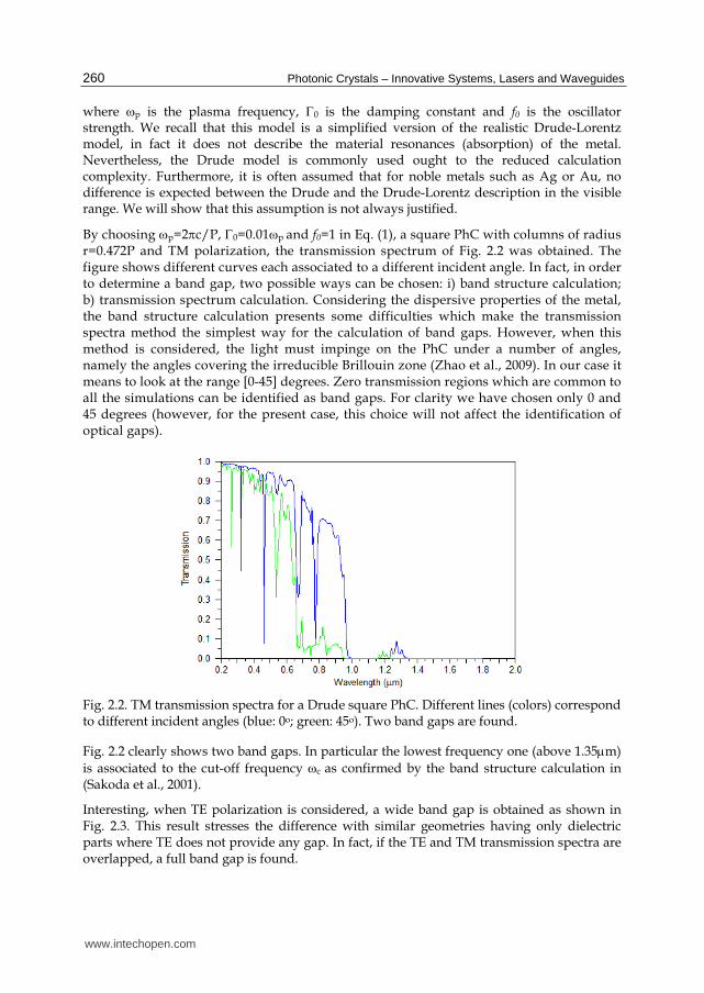
By choosing p=2c/P, 0=0.01p and f0=1 in Eq. (1), a square PhC with columns of radius r=0.472P and TM polarization, the transmission spectrum of Fig. 2.2 was obtained. The figure shows different curves each associated to a different incident angle. In fact, in order to determine a band gap, two possible ways can be chosen: i) band structure calculation; b) transmission spectrum calculation. Considering the dispersive properties of the metal, the band structure calculation presents some difficulties which make the transmission spectra method the simplest way for the calculation of band gaps. However, when this method is considered, the light must impinge on the PhC under a number of angles, namely the angles covering the irreducible Brillouin zone (Zhao et al., 2009). In our case it means to look at the range [0-45] degrees. Zero transmission regions which are common to all the simulations can be identified as band gaps. For clarity we have chosen only 0 and 45 degrees (however, for the present case, this choice will not affect the identification of optical gaps).
Fig. 2.2. TM transmission spectra for a Drude square PhC. Different lines (colors) correspond to different incident angles (blue: 0o; green: 45o). Two band gaps are found.
Fig. 2.2 clearly shows two band gaps. In particular the lowest frequency one (above 1.35m) is associated to the cut-off frequency c as confirmed by the band structure calculation in (Sakoda et al., 2001).
Interesting, when TE polarization is considered, a wide band gap is obtained as shown in Fig. 2.3. This result stresses the difference with similar geometries having only dielectric parts where TE does not provide any gap. In fact, if the TE and TM transmission spectra are overlapped, a full band gap is found.
www.intechopen.com
Photonic Crystals for Plasmonics: From Fundamentals to Superhydrophobic Devices
261
Fig. 2.3. TE transmission spectra for a Drude square PhC. Different lines (colors) correspond to different incident angles (blue: 0o; green: 45o).
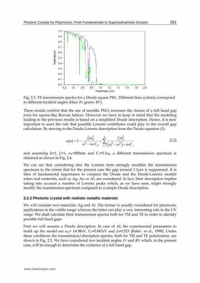
These results confirm that the use of metallic PhCs increases the chance of a full band gap even for square-like Bravais lattices. However we have to keep in mind that the modeling leading to the previous results is based on a simplified Drude description. Hence, it is now important to asset the role that possible Lorentz contributes could play in the overall gap calculation. By moving to the Drude-Lorentz description from the Drude equation (1):
2 2
02 2 2
10
( ) 1k
p j p
j j j
f f
i i
(2.2)
and assuming k=1, f1=1, 1=800nm and 1=0.1p a different transmission spectrum is obtained as shown in Fig. 2.4.
We can see that considering also the Lorentz term strongly modifies the transmission spectrum to the extent that for the present case the gap around 1.1m is suppressed. It is then of fundamental importance to compare the Drude and the Drude-Lorentz models when real materials, such as Ag, Au or Al, are considered. In fact, their description implies taking into account a number of Lorentz peaks which, as we have seen, might strongly modify the transmission spectrum compared to a simple Drude description.
2.2.2 Photonic crystal with realistic metallic materials
We will consider two materials: Ag and Al. The former is usually considered for plasmonic applications in the visible range whereas the latter can play a very interesting role in the UV range. We shall calculate their transmission spectra both for TM and TE in order to identify possible full band gaps.
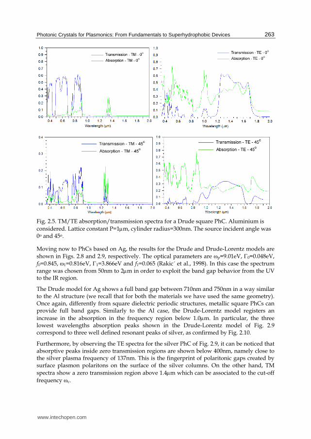
First we will assume a Drude description. In case of Al, the experimental parameters to build up the model are p= 14.98eV, 0=0.047eV and f0=0.523 (Rakic´ et al., 1998). Under these conditions the transmission/absorption spectra, both for TM and TE polarization, are shown in Fig. 2.5. We have considered two incident angles, 0o and 45o which, in the present case, will be enough to determine the existence of a full band gap.
www.intechopen.com
Photonic Crystals – Innovative Systems, Lasers and Waveguides
262
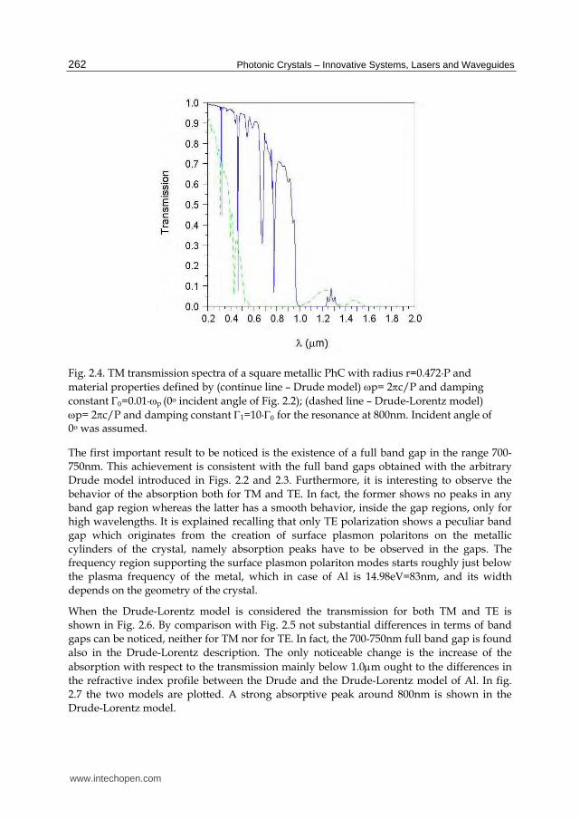
Fig. 2.4. TM transmission spectra of a square metallic PhC with radius r=0.472·P and material properties defined by (continue line – Drude model) p= 2c/P and damping constant =0.01·p (0o incident angle of Fig. 2.2); (dashed line – Drude-Lorentz model) p= 2c/P and damping constant 1=10· for the resonance at 800nm. Incident angle of 0o was assumed.
The first important result to be noticed is the existence of a full band gap in the range 700-750nm. This achievement is consistent with the full band gaps obtained with the arbitrary Drude model introduced in Figs. 2.2 and 2.3. Furthermore, it is interesting to observe the behavior of the absorption both for TM and TE. In fact, the former shows no peaks in any band gap region whereas the latter has a smooth behavior, inside the gap regions, only for high wavelengths. It is explained recalling that only TE polarization shows a peculiar band gap which originates from the creation of surface plasmon polaritons on the metallic cylinders of the crystal, namely absorption peaks have to be observed in the gaps. The frequency region supporting the surface plasmon polariton modes starts roughly just below the plasma frequency of the metal, which in case of Al is 14.98eV=83nm, and its width depends on the geometry of the crystal.
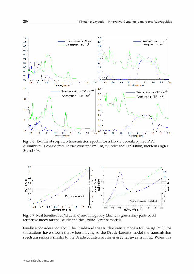
When the Drude-Lorentz model is considered the transmission for both TM and TE is shown in Fig. 2.6. By comparison with Fig. 2.5 not substantial differences in terms of band gaps can be noticed, neither for TM nor for TE. In fact, the 700-750nm full band gap is found also in the Drude-Lorentz description. The only noticeable change is the increase of the absorption with respect to the transmission mainly below 1.0m ought to the differences in the refractive index profile between the Drude and the Drude-Lorentz model of Al. In fig. 2.7 the two models are plotted. A strong absorptive peak around 800nm is shown in the Drude-Lorentz model.
www.intechopen.com
Photonic Crystals for Plasmonics: From Fundamentals to Superhydrophobic Devices
263
Fig. 2.5. TM/TE absorption/transmission spectra for a Drude square PhC. Aluminium is considered. Lattice constant P=1m, cylinder radius=300nm. The source incident angle was 0o and 45o.
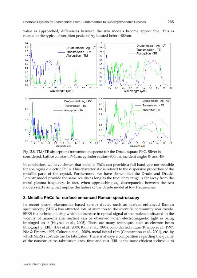
Moving now to PhCs based on Ag, the results for the Drude and Drude-Lorentz models are shown in Figs. 2.8 and 2.9, respectively. The optical parameters are p=9.01eV, 0=0.048eV, f0=0.845, 1=0.816eV, 1=3.866eV and f1=0.065 (Rakic´ et al., 1998). In this case the spectrum range was chosen from 50nm to 2m in order to exploit the band gap behavior from the UV to the IR region.
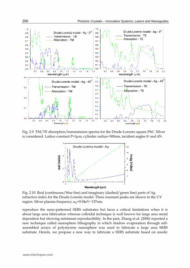
The Drude model for Ag shows a full band gap between 710nm and 750nm in a way similar to the Al structure (we recall that for both the materials we have used the same geometry). Once again, differently from square dielectric periodic structures, metallic square PhCs can provide full band gaps. Similarly to the Al case, the Drude-Lorentz model registers an increase in the absorption in the frequency region below 1.0m. In particular, the three lowest wavelengths absorption peaks shown in the Drude-Lorentz model of Fig. 2.9 correspond to three well defined resonant peaks of silver, as confirmed by Fig. 2.10.
Furthermore, by observing the TE spectra for the silver PhC of Fig. 2.9, it can be noticed that absorptive peaks inside zero transmission regions are shown below 400nm, namely close to the silver plasma frequency of 137nm. This is the fingerprint of polaritonic gaps created by surface plasmon polaritons on the surface of the silver columns. On the other hand, TM spectra show a zero transmission region above 1.4m which can be associated to the cut-off frequency c.
www.intechopen.com
Photonic Crystals – Innovative Systems, Lasers and Waveguides
264
Fig. 2.6. TM/TE absorption/transmission spectra for a Drude-Lorentz square PhC. Aluminium is considered. Lattice constant P=1m, cylinder radius=300nm, incident angles 0o and 45o.
Fig. 2.7. Real (continuous/blue line) and imaginary (dashed/green line) parts of Al refractive index for the Drude and the Drude-Lorentz models.
Finally a consideration about the Drude and the Drude-Lorentz models for the Ag PhC. The simulations have shown that when moving to the Drude-Lorentz model the transmission spectrum remains similar to the Drude counterpart for energy far away from p. When this
www.intechopen.com
Photonic Crystals for Plasmonics: From Fundamentals to Superhydrophobic Devices
265
value is approached, differences between the two models become appreciable. This is related to the typical absorption peaks of Ag located before 400nm.
Fig. 2.8. TM/TE absorption/transmission spectra for the Drude square PhC. Silver is considered. Lattice constant P=1m, cylinder radius=300nm, incident angles 0o and 45o.
In conclusion, we have shown that metallic PhCs can provide a full band gap not possible for analogues dielectric PhCs. This characteristic is related to the dispersive properties of the metallic parts of the crystal. Furthermore, we have shown that the Drude and Drude-Lorentz model provide the same results as long as the frequency range is far away from the metal plasma frequency. In fact, when approaching p, discrepancies between the two models start rising that implies the failure of the Drude model at low frequencies.
3. Metallic PhCs for surface enhanced Raman spectroscopy
In recent years, plasmonics based sensor device such as surface enhanced Raman spectroscopy (SERS) has attracted lots of attention to the scientific community worldwide. SERS is a technique using which an increase in optical signal of the molecule situated in the vicinity of nano-metallic surface can be observed when electromagnetic light is being impinged on it (Haynes et al., 2005). There are many techniques such as electron beam lithography (EBL) (Das et al., 2009; Kahl et al., 1998), colloidal technique (Kneipp et al., 1997; Nie & Emory, 1997; Coluccio et al., 2009), metal island film (Constantino et al., 2001), etc. by which SERS substrate can be fabricated. There is always a competition regarding the quality of the nanostructure, fabrication area, time and cost. EBL is the most efficient technique to
www.intechopen.com
Photonic Crystals – Innovative Systems, Lasers and Waveguides
266
Fig. 2.9. TM/TE absorption/transmission spectra for the Drude-Lorentz square PhC. Silver is considered. Lattice constant P=1m, cylinder radius=300nm, incident angles 0o and 45o.
Fig. 2.10. Real (continuous/blue line) and imaginary (dashed/green line) parts of Ag refractive index for the Drude-Lorentz model. Three resonant peaks are shown in the UV region. Silver plasma frequency p=9.04eV~137nm.
reproduce the nano-patterned SERS substrates but faces a critical limitations when it is about large area fabrication whereas colloidal technique is well known for large area metal deposition but showing minimum reproducibility. In the past, Zhang et al. (2006) reported a new technique called nanosphere lithography in which shadow evaporation through self-assembled arrays of polystyrene nanosphere was used to fabricate a large area SERS substrate. Herein, we propose a new way to fabricate a SERS substrate based on anodic
www.intechopen.com
Photonic Crystals for Plasmonics: From Fundamentals to Superhydrophobic Devices
267
porous alumina (APA) which could be a trade-off between the two above limits such as large fabrication area and SERS enhancement factor.
In the present work, APA substrate, having hexagonal periodicity, has been fabricated. The fabricated APA substrates were used as templates for the preparation of nanopatterned gold surfaces, obtained by gold film deposition of ~25 nm thickness covering the APA features. Using this technique, we are able to achieve reproducible SERS substrates with the wall thickness and pore diameter down to 40 and 60 nm, respectively. It is noticeable that the substrate shows very efficient SERS signal even in presence of intrinsically fluorescent molecules. The substrate surface morphology was characterized by both atomic force microscopy (AFM) and scanning electron microscopy (SEM), and the performance as a SERS substrate was tested with cresyl violet (CV). These substances fluoresce at distinct wavelengths in the visible spectrum from red to violet region. Even if it is known that nano-metallic surface acts as a fluorescence quenching substrate (Dulkeith et al., 2002), it is the first time, in our knowledge, that the large area SERS substrate on APA template was employed for SERS analysis in such detail.
In order to provide the surfaces with plasmon functionality, gold was thermally evaporated from a tungsten boat onto the APA substrates (APA), starting the deposition at a base chamber pressure of 2.0x10⁻⁶ mbar and proceeding at a 0.5 Å/s until a final total thickness of ~25 nm was reached. During deposition the sample holder was rotated at 1 RPM in order to improve the uniformity and the morphological quality of the gold layer. The substance of interest was deposited over resulting gold-coated APA substrate (termed ‘AuAPA’) using chemisorption technique. In this process, the substrate was dipped in a solution containing the molecule of interest. After incubation, the substrate was removed from the solution, gently rinsed to remove excess molecules those are not attached directly to the metal surface. Thereafter, the samples were dried in N2 flow, and finally stored in a desiccator before SERS measurements. Cresyl violet (CV) dyes was tested for SERS probes with the concentration in the order of 10-6 M.
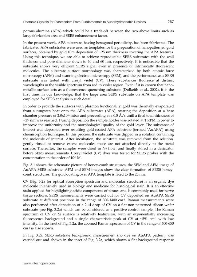
Fig. 3.1 shows the schematic picture of honey-comb structures, the SEM and AFM image of AuAPA SERS substrate. AFM and SEM images show the clear formation of SERS honey-comb structures. The gold-coating over APA template is fixed to the 25 nm.
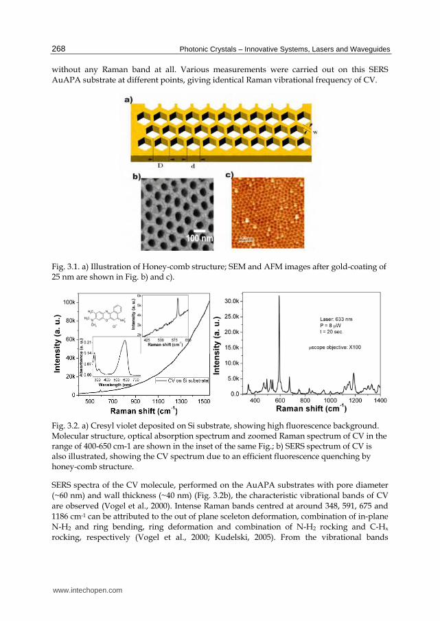
CV (Fig. 3.2a for optical absorption spectrum and molecular structure) is an organic dye molecule intensively used in biology and medicine for histological stain. It is an effective stain applied for highlighting acidic components of tissues and is commonly used for nerve tissue sections. SERS measurements were carried out for CV deposited on AuAPA SERS substrate at different positions in the range of 300-1400 cm-1. Raman measurements were also performed after deposition of a 2 l drop of CV on a flat non-patterned silicon wafer substrate (see Fig. 3.2a) which can be considered as a positive control sample. The Raman spectrum of CV on Si surface is relatively featureless, with an exponentially increasing fluorescence background and a single characteristic peak of CV at ~591 cm-1 with low intensity. In the inset of Fig. 3.2a, the zoomed Raman spectrum of CV in the range of 400-650 cm-1 is also shown.
In Fig. 3.2a, SERS substrate background measurement (no dye on AuAPA pattern) was carried out and shown in the inset of Fig. 3.2a, which shows a flat background response
www.intechopen.com
Photonic Crystals – Innovative Systems, Lasers and Waveguides
268
without any Raman band at all. Various measurements were carried out on this SERS AuAPA substrate at different points, giving identical Raman vibrational frequency of CV.
Fig. 3.1. a) Illustration of Honey-comb structure; SEM and AFM images after gold-coating of 25 nm are shown in Fig. b) and c).
Fig. 3.2. a) Cresyl violet deposited on Si substrate, showing high fluorescence background. Molecular structure, optical absorption spectrum and zoomed Raman spectrum of CV in the range of 400-650 cm-1 are shown in the inset of the same Fig.; b) SERS spectrum of CV is also illustrated, showing the CV spectrum due to an efficient fluorescence quenching by honey-comb structure.
SERS spectra of the CV molecule, performed on the AuAPA substrates with pore diameter (~60 nm) and wall thickness (~40 nm) (Fig. 3.2b), the characteristic vibrational bands of CV are observed (Vogel et al., 2000). Intense Raman bands centred at around 348, 591, 675 and 1186 cm-1 can be attributed to the out of plane sceleton deformation, combination of in-plane N-H2 and ring bending, ring deformation and combination of N-H2 rocking and C-Hx rocking, respectively (Vogel et al., 2000; Kudelski, 2005). From the vibrational bands
www.intechopen.com
Photonic Crystals for Plasmonics: From Fundamentals to Superhydrophobic Devices
269
observed in the Fig. 3.2b it is most probable that the CV is oriented in such a way that the –N-H2 group is closer to the gold film, leading to the strong Raman scattering and, consequently, higher Raman signal. Additionally, in Fig. 3.2b, the high exponential background appeared in Fig. 3.2a for the CV on silicon substrate has disappeared. Hence, significant fluorescence quenching is also illustrated, as already observed in the past for gold nanoparticles (Dulkeith et al., 2002). SERS substrate background measurement (no dye on AuAPA pattern) was carried out and found a flat background response without any Raman band at all.
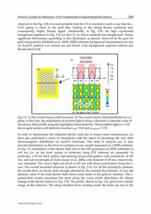
Fig. 3.3. a) The overall honey-comb structure. b) The overall electric field distribution in x-y plane, in this case, the polarization of incident light is along x-direction; c) absolute value of the electric field profile along the highlighted horizontal line. The excitation light is = 633 nm on gold surface with dielectric function real= 9.83 and imaginary= 1.97.
In order to demonstrate the enhanced electric field due to honey-comb nanostructure, we have also performed a series of simulations with the intent of calculating the near field electromagnetic distribution on AuAPA substrates. This kind of analysis can, in fact, provide information on the level of excitation of any sample deposited on a SERS substrate. In Fig. 3.3, simulations of the electric field due to the LSP generation on SERS substrates at z=0 nm (i.e. on the front surface of substrate) using CST software are presented. In particular, a 25 nm thick golden slab showing honeycomb pattern with periodicity of 100 nm, and sub-wavelength air holes (Lezec et al., 2004) with diameter of 60 nm, respectively, was simulated. The source light was fixed to 633 nm with linear polarization along the x-axis. The overall simulated structure is shown in Fig. 3.3a. For all the periodicity patterns, the results show an electric field strongly affected by the material discontinuity. In fact, the absolute value of the total electric field shows some nodes at the gold-air interface. The x-polarization creates anti-phase hot spots along the x-axis which determines the abrupt change of the electric field as in Fig. 3.3b. The profile, shown in Fig. 3.3c, gives even a better image of this behavior. The sharp doubled horns existing inside the holes are due to the
www.intechopen.com
Photonic Crystals – Innovative Systems, Lasers and Waveguides
270
hexagonal geometry of the holes. Important features emerging from the simulations are both the mean (Emean) and the effective (Eeff) value of the electric field outside the holes (shaded regions in Fig. 3.3c). The former is simply defined as the average field whereas the latter is given by the difference between the maximum and minimum values in the hole.
In conclusion, home-built AuAPA substrates with pore size of 60 nm and wall thickness of 40 nm was utilized for large area SERS substrates. CV was deposited using chemisorption technique, using which a monolayer of molecules can be achieved. CST simulations of the electric field distribution on these ordered and reproducible SERS substrates were also performed, keeping the structural parameters as close as possible to the experimental honey-comb nanostructures. Theoretical results follow the same trend of experimental findings. The major advantage of using nanoporous alumina substrates, as compared to the traditional colloidal coating or lithographic processing, is a good trade-off between the high enhancement factor ‘G’ obtained and the large surface area produced. The respective SERS enhancement factor ‘G’ is estimated to be ~4106.
Further research should be made in order to optimize ‘G’ on the basis of the substrate parameters of pore size, wall thickness, and thickness of the gold coating. The next step towards reproducible micro-fabricated SERS devices would be the transfer of APA to technological substrates such as optical glass or silicon wafer, and combining APA patterning with optical lithography. In this way, large-area SERS bio- and chemical sensors assays for e.g. parallel biomedical screening of different body liquids or even tissues could be carried out, conveniently. The easy and inexpensive processing required for APA SERS fabrication would also make these substrates disposable, opening the way to their large scale applications. Such a high SERS enhancement as demonstrated here can provide single molecule sensitivity in a sensor based on labeling using fluorescence dyes.
4. Integration of biophotonics and superhydrophobic devices for the detection of few bio-molecules
In biomedical disciplines including medicine, biology or biotechnology, there is a huge interest in understanding the pathogenesis of diseases, and to develop new biomarkers for their diagnosis. In particular, early detection can lead to significant benefits in terms of efficient and timely treatment. In these regards, the blood contains a multitude of unstudied and unknown biomarkers that could reflect the ongoing physiologic state of tissues and organs. The low-molecular weight region of the blood proteome is an important source of diagnostic markers (Posadas et al., 2001). Nevertheless, this 'mine' of data for diagnosis is often practically inaccessible by conventional approaches, in that the solutions at study are extremely diluted, and contain a multitude of substances that would blur the signal of interest. To exploit this 'mine' of data for diagnosis, new devices are required with very low detection limits. Nanotechnology, as a whole, offers unprecedented opportunities to realize such devices, thus increasing the efficacy of diagnosis (Liotta et al., 2003). In the paragraphs above, the theory of plasmons and the use of plasmonic devices have been largely described. Here, the integration of this technology with superhydrophobic surfaces (SHSs) is introduced.
The aim of this paragraph is to expound on the contributions that this combination can possibly offer to clinical medicine, specifically in the discipline of early diagnostics. In particular, it revolves around the study and the micro/nano fabrication of SHSs which
www.intechopen.com
Photonic Crystals for Plasmonics: From Fundamentals to Superhydrophobic Devices
271
incorporate biophotonic devices. Well assessed mechanisms such as (i) superhydrophobicity and (ii) SERS (Surface Enhanced Raman Scattering) are recapitulated and integrated into a single micro- nano- system. The combination of these two would represent a boost towards the detection and the analysis of few (or single) molecules. In the following, SHSs and nano optics based photonic devices are treated separately. After an introduction of the most important features of these, their combination and the effects thereof are discussed. Notice that, differently from plasmonic devices, SHSs are exposed to a good detail in that they are introduced here for the first time in the text.
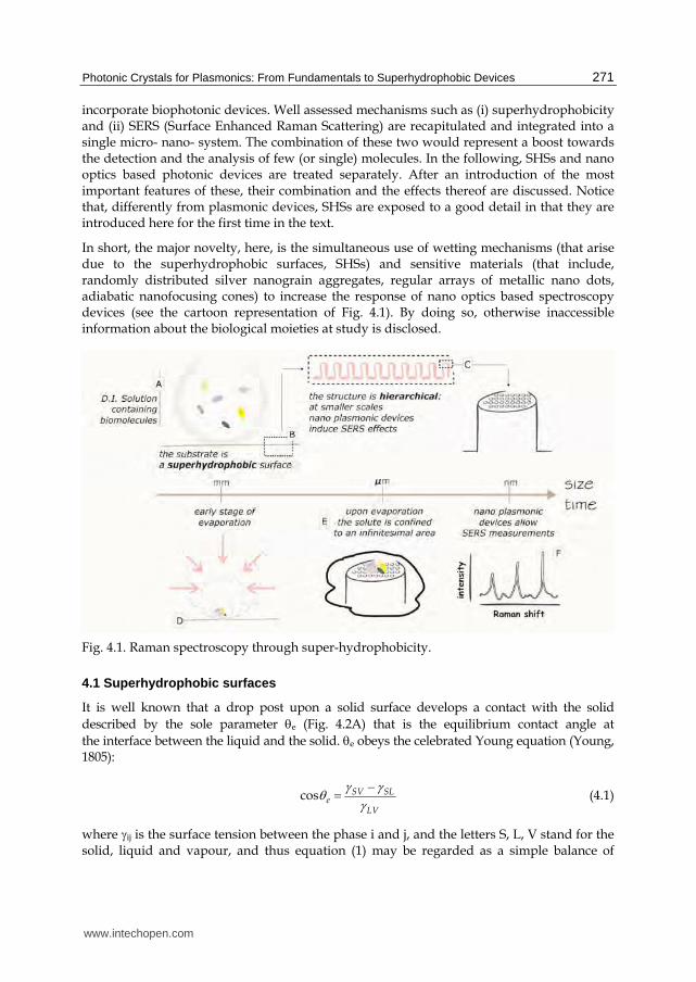
In short, the major novelty, here, is the simultaneous use of wetting mechanisms (that arise due to the superhydrophobic surfaces, SHSs) and sensitive materials (that include, randomly distributed silver nanograin aggregates, regular arrays of metallic nano dots, adiabatic nanofocusing cones) to increase the response of nano optics based spectroscopy devices (see the cartoon representation of Fig. 4.1). By doing so, otherwise inaccessible information about the biological moieties at study is disclosed.
Fig. 4.1. Raman spectroscopy through super-hydrophobicity.
4.1 Superhydrophobic surfaces
It is well known that a drop post upon a solid surface develops a contact with the solid described by the sole parameter e (Fig. 4.2A) that is the equilibrium contact angle at the interface between the liquid and the solid. e obeys the celebrated Young equation (Young, 1805):
cos SV SLe
LV
(4.1)
where ij is the surface tension between the phase i and j, and the letters S, L, V stand for the solid, liquid and vapour, and thus equation (1) may be regarded as a simple balance of
www.intechopen.com
Photonic Crystals – Innovative Systems, Lasers and Waveguides
272
forces. For sufficiently small droplets the dominant force becomes the liquid-vapor surface tension and gravitation may be neglected. The dimensionless Bond number can be consequently introduced as Bo=×g×R2/LV, where is the density of the liquid, R is the radius of the spherical drop prior the deposition upon the surface, and g is the acceleration due to gravity. When Bo<<1 gravitational effects vanish and the shape of the droplet may be assumed spherical everywhere. For a drop of water with LV=72.9 mJ/m2, =1000 kg/m3, and diameter d=2×R=1 mm, it follows that Bo~0.035, and thus the physics of micrometric or submillimetric drops is correctly governed by surface tension solely.
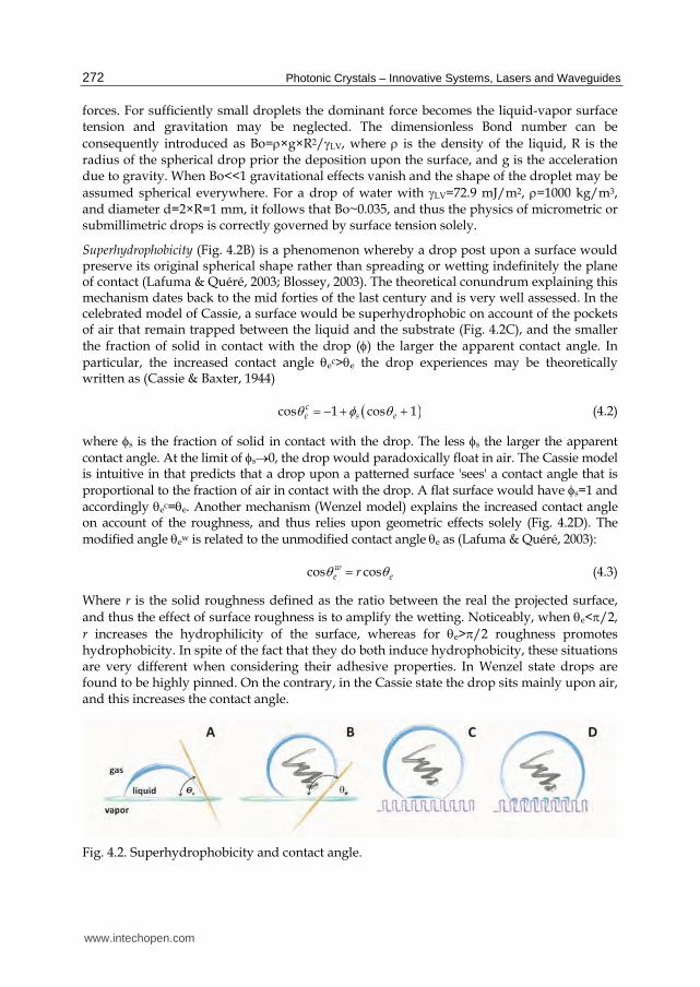
Superhydrophobicity (Fig. 4.2B) is a phenomenon whereby a drop post upon a surface would preserve its original spherical shape rather than spreading or wetting indefinitely the plane of contact (Lafuma & Quéré, 2003; Blossey, 2003). The theoretical conundrum explaining this mechanism dates back to the mid forties of the last century and is very well assessed. In the celebrated model of Cassie, a surface would be superhydrophobic on account of the pockets of air that remain trapped between the liquid and the substrate (Fig. 4.2C), and the smaller the fraction of solid in contact with the drop () the larger the apparent contact angle. In particular, the increased contact angle ec>e the drop experiences may be theoretically written as (Cassie & Baxter, 1944)
cos 1 cos 1ce s e (4.2)
where s is the fraction of solid in contact with the drop. The less s the larger the apparent contact angle. At the limit of s0, the drop would paradoxically float in air. The Cassie model is intuitive in that predicts that a drop upon a patterned surface 'sees' a contact angle that is proportional to the fraction of air in contact with the drop. A flat surface would have s=1 and accordingly ec=e. Another mechanism (Wenzel model) explains the increased contact angle on account of the roughness, and thus relies upon geometric effects solely (Fig. 4.2D). The modified angle ew is related to the unmodified contact angle e as (Lafuma & Quéré, 2003):
cos coswe er (4.3)
Where r is the solid roughness defined as the ratio between the real the projected surface, and thus the effect of surface roughness is to amplify the wetting. Noticeably, when e</2, r increases the hydrophilicity of the surface, whereas for e>/2 roughness promotes hydrophobicity. In spite of the fact that they do both induce hydrophobicity, these situations are very different when considering their adhesive properties. In Wenzel state drops are found to be highly pinned. On the contrary, in the Cassie state the drop sits mainly upon air, and this increases the contact angle.
Fig. 4.2. Superhydrophobicity and contact angle.
www.intechopen.com
Photonic Crystals for Plasmonics: From Fundamentals to Superhydrophobic Devices
273
In the Cassie state the drop would roll upon the surface and it would progressively reduce its contact area during a process of evaporation. The drop would then maintain the Cassie state over time, thus avoiding collapse and any irreversible transition to Wenzel until a critical radius of impalement is achieved. The mechanisms inducing collapse in a slowly evaporating droplet are two and, namely, (i) the drop could either touch the surface below the posts, or (ii) the surface free energy gained as the drop collapses wins over the surface free energy lost by increased contact with the hydrophobic posts. While the first mechanism regards surfaces decorated with short posts or pillars, the second relies upon an energetic argument and is independent on the pillars' height. In many practical situations one should consider the latter criterion solely (De Angelis et al., 2011). In particular, both analytical calculations and numerical simulations show that the critical radius of impalement depends upon the distance between the pillars and e as
min cos e
r (4.4)
and thus the closer the pillars the smaller the final area of contact. From the analysis above it stems out that surfaces with large (that is, with sufficiently dense pillars), would guarantee a stable Cassie configuration. Notice though that large would induce small contact angles, and thus the choice for the best design parameters is not trivial, and it is indeed a matter of optimization.
SHSs retain unique properties in terms of wettability that can be reviewed as follows: (i) SHSs have superior adhesive properties, in the sense that they exhibit vanishing friction coefficients; (ii) a droplet, post upon these surfaces, would accordingly preserve a quasi-spherical shape while evaporates, and the contact area at the interface would thus progressively reduce; (iii) SHSs can be artificially reproduced using micro and nano fabrication techniques. Using the properties above, micro textured surfaces may be successfully exploited to concentrate tiny amounts of moities over micrometric areas, and consequently measure these moieties with unprecedented accuracy (De Angelis et al., 2011; Accardo et al., 2011; Gentile et al., 2011a; Gentile et al., 2011b; Di Fabrizio et al., 2008).
4.1.1 Fabrication of SHSs
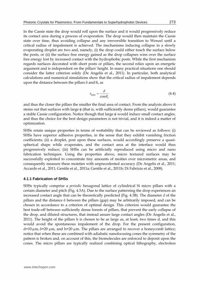
SHSs typically comprise a periodic hexagonal lattice of cylindrical Si micro pillars with a certain diameter and pitch (Fig. 4.3A). Due to the surface patterning the drop experiences an increased contact angle that can be theoretically predicted (Fig. 4.3B). The diameter d of the pillars and the distance between the pillars (gap) may be arbitrarily imposed, and can be chosen in accordance to a criterion of optimal design. This criterion would guarantee the best trade-off between sufficiently dense forests of pillars, that prevent the early collapse of the drop, and diluted structures, that instead assure large contact angles (De Angelis et al., 2011). The height of the pillars h is chosen to be as large as, at least, two times d, and this would avoid the spontaneous impalement of the drop. For the present configuration, d=10m,=20 m, and h=20 m. The pillars are arranged to recover a honeycomb lattice; notice that when these are combined with adiabatic nanofocusing cones the symmetry of the pattern is broken and, on account of this, the biomolecules are enforced to deposit upon the cones. The micro pillars are typically realized combining optical lithography, electroless
www.intechopen.com
Photonic Crystals – Innovative Systems, Lasers and Waveguides
274
growth and Bosch Reactive Ion Etching (RIE) techniques. Non conventional biophotonic nanostructures as those described below, conveniently positioned upon the pillars, would complete a hierarchical structure thus permitting the identification of proteins in the single molecule regime (Fig. 4.3C). These 'two-stages' micro nano structures function as SHSs with an increased contact angle ranging from 155° to about 175°.
Fig. 4.3. SEM image of a photonic crystal for superhydrophobicity applications.
4.1.2 Current applications of SHSs
Many applications exist revolving around the use of superhydrophobic surfaces and mainly founding upon two key features of these, that are the limited contact area and the ability of a drop to slide or slip upon such surfaces (Li et al., 2007). Water repellent coatings for radar domes, satellite dishes and glass are widely reported and currently in use. These coatings provide self-cleaning under the action of rain in that they mimic the self-cleaning action of the Lotus leaf. Other utilizations include antibiofouling paints for boats, antisticking of snow for antennas and windows, self-cleaning windshields for automobiles, the separation of water and oil, and the manufacture of water-proof fireretardant clothes. The latter would represent examples of a target market that is the huge household-commodity sector, nevertheless new analytical potentials also do exist which carry the promise of unparalleled opportunities in life sciences and in the high tech field of biotechnology. In Biotechnology many efforts are devoted to manipulate, control and analyse relevant molecules as DNA and proteins, and artificially (nanotech) fabricated superhydrophobic surfaces could be an effective advance towards this objective. Let's consider, for instance, the case of microarrays. These are libraries of biological or chemical entities (probes) immobolised in a grid on a solid surface, the probes would be then interacting with targets (i.e., geneses, proteins, cDNA...) to provide deep insight into DNA sequences. It is desirable that the drop containing the targets would evaporate avoiding pinning and the formation of noxious ring like structures (it is in fact well known that pinning during evaporations causes final solute formations disposed in doughnut shape, and this is commonly known as the coffee-ring effect, and here suitable superhydrophobic substrates come into play.
The transport, separation and mixing of moieties dispersed in droplets has an enormous interest likewise. Superhydrophobic surfaces are slippy, and thus a droplet would move upon the application of an infinitesimal external force field: tilting the surface (and thus gravitation) or electrostatic or surface waves induced force fields would move the droplet in a controllable way (see also below in materials and methods). On the other hand, variations in the patterning or texture of the surface would generate regions where the adhesive
www.intechopen.com
Photonic Crystals for Plasmonics: From Fundamentals to Superhydrophobic Devices
275
properties are also different, thus creating well defined and distinguished tracks or patterns, and the drop could be exteriorly positioned into a precise area or point of the substrate. This argument is the ground for novel droplet-based microfluidic systems as reported in a number or publications and patents, and these surface would be in fact lab-on-chip systems which deliver the ability of performing bio-chemical detections and reactions with incomparable accuracy and efficiency. Recently, the use of superhydrophobic surfaces to concentrate and localize a solute has been proposed.
4.2 BioPhotonic devices
Biophotonic nanostructures can be integrated to SHSs to obtain devices with advanced sensing capabilities. Here we shall recapitulate in short specific types of nano-geometry based plasmonic device, and namely (i) electroless grown random assemblies of silver nanograins; (ii) regular arrays of metallic nano dots; (iii) adiabatic nanofocusing cones. Nevertheless, the method can be extended to a number of different plasmonic nanostructures, as those broadly described in the paragraphs above (De Angelis et al., 2011; Accardo et al., 2011; Gentile et al., 2011a; Gentile et al., 2011b; Di Fabrizio et al., 2008; Gentile et al., 2010).
4.2.1 Electroless grown silver nanograins
The electroless growth is a process whereby ionic silver is reduced and deposited as metallic silver upon silicon, via a redox reaction, and according to a mechanism that may be adequately described by a diffusion limited aggregation model. A satisfactory comprehension of the method may be found in (Coluccio et al., 2009). Here it is briefly recalled that, conveniently employing this process, and depending upon the growth parameters, silver nanograins may be obtained with an average size as small as few tens of nanometers, which compose efficient SERS substrates (Fig. 4.4A).
Fig. 4.4. SEM images of a metallic photonic crystal and plasmonic device.
4.2.2 Regular arrays of metallic nano dots
These are gold or silver hemisphere positioned upon the substrate as to reproduce a regular square lattice. Optical lithography, electron beam lithography, Reactive Ion Etching, evaporation techniques are routinely used for the fabrication of these devices. Differently from the case above, the shape, dimension, position of the dots is deterministic in the limit of the fabrication process. Thereby SERS effects arise from the rational design of the nano
www.intechopen.com
Photonic Crystals – Innovative Systems, Lasers and Waveguides
276
structure, founding upon the theory of surface plasmon polariton scattering (Fig. 4.4B) (De Angelis et al., 2011).
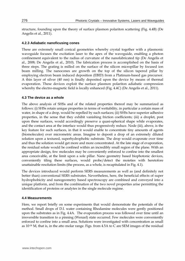
4.2.3 Adiabatic nanoficusing cones
These are extremely small conical geometries whereby crystal together with a plasmonic waveguide focuses the excitation laser to the apex of the waveguide, enabling a photon confinement equivalent to the radius of curvature of the nanofabricated tip (De Angelis et al., 2008; De Angelis et al., 2010). The fabrication process is accomplished on the basis of three steps. The grating is milled on the surface of the silicon micropillar by focused ion beam milling. The nanocones are growth on the top of the silicon tapered pillar by employing electron beam induced deposition (EBID) from a Platinum-based gas precursor. A thin layer of silver (40 nm) is finally deposited upon the device by means of thermal evaporation. These devices exploit the surface plasmon polariton adiabatic compression whereby the electro-magnetic field is locally enhanced (Fig. 4.4C) (De Angelis et al., 2011).
4.3 The device as a whole
The above analysis of SHSs and of the related properties thereof may be summarized as follows: (i) SHSs retain unique properties in terms of wettability, in particular a certain mass of water, in shape of a drop, would be repelled by such surfaces; (ii) SHSs have superior adhesive properties, in the sense that they exhibit vanishing friction coefficients; (iii) a droplet, post upon these surfaces, would accordingly preserve a quasi-spherical shape while evaporates, and the contact area at the interface would thus progressively reduce. Node (iii), above, is the key feature for such surfaces, in that it would enable to concentrate tiny amounts of agents (biomolecules) over micrometric areas. Imagine to deposit a drop of an extremely diluted solution upon a textured, superhydrophobic substrate. The drop would evaporate over time and thus the solution would get more and more concentrated. At the late stage of evaporation, the residual solute would be confined within an incredibly small region of the plane. With an appropriate design, few molecules may be conveniently enforced to confine into the smallest area conceivable, at the limit upon a sole pillar. Nano geometry based biophotonic devices, conveniently tiling these surfaces, would probe/detect the moieties with heretofore unattainable resolution limits (the process, as a whole, is recapitulated in Fig. 4.1).
The devices introduced would perform SERS measurements as well as (and definitely not better than) conventional SERS substrates. Nevertheless, here, the beneficial effects of super hydrophobicity and nanogeometry based spectroscopy are combined and conveyed into a unique platform, and from the combination of the two novel properties arise permitting the identification of proteins or analytes in the single molecule regime.
4.4 Measurements
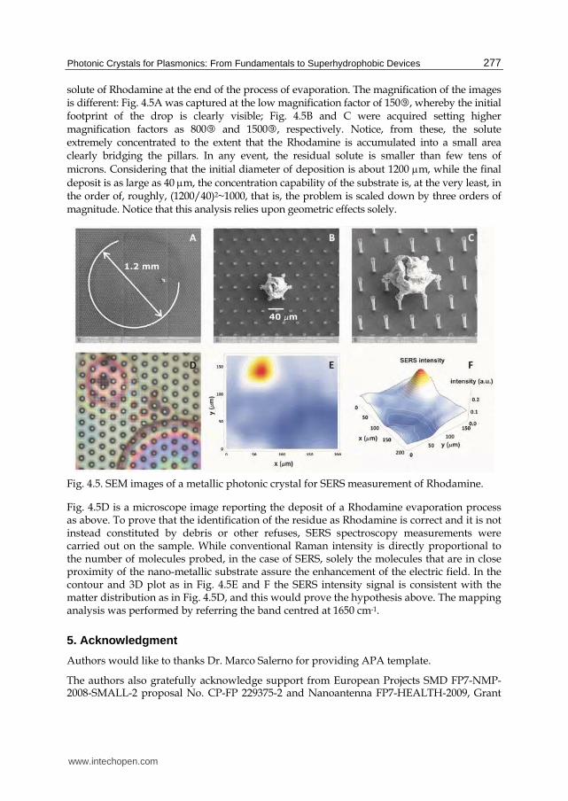
Here, we report briefly on some experiments that would demonstrate the potentials of the method. Small drops of D.I. water containing Rhodamine molecules were gently positioned upon the substrates as in Fig. 4.4A. The evaporation process was followed over time until an irreversible transition to a pinning (Wenzel) state occurred. Few molecules were conveniently enforced to confine into a small area. Solutions were investigated with concentration as small as 10-18 M, that is, in the atto molar range. Figs. from 4.5A to C are SEM images of the residual
www.intechopen.com
Photonic Crystals for Plasmonics: From Fundamentals to Superhydrophobic Devices
277
solute of Rhodamine at the end of the process of evaporation. The magnification of the images is different: Fig. 4.5A was captured at the low magnification factor of 150, whereby the initial footprint of the drop is clearly visible; Fig. 4.5B and C were acquired setting higher magnification factors as 800 and 1500, respectively. Notice, from these, the solute extremely concentrated to the extent that the Rhodamine is accumulated into a small area clearly bridging the pillars. In any event, the residual solute is smaller than few tens of microns. Considering that the initial diameter of deposition is about 1200 m, while the final deposit is as large as 40 m, the concentration capability of the substrate is, at the very least, in the order of, roughly, (1200/40)2~1000, that is, the problem is scaled down by three orders of magnitude. Notice that this analysis relies upon geometric effects solely.
Fig. 4.5. SEM images of a metallic photonic crystal for SERS measurement of Rhodamine.
Fig. 4.5D is a microscope image reporting the deposit of a Rhodamine evaporation process as above. To prove that the identification of the residue as Rhodamine is correct and it is not instead constituted by debris or other refuses, SERS spectroscopy measurements were carried out on the sample. While conventional Raman intensity is directly proportional to the number of molecules probed, in the case of SERS, solely the molecules that are in close proximity of the nano-metallic substrate assure the enhancement of the electric field. In the contour and 3D plot as in Fig. 4.5E and F the SERS intensity signal is consistent with the matter distribution as in Fig. 4.5D, and this would prove the hypothesis above. The mapping analysis was performed by referring the band centred at 1650 cm-1.
5. Acknowledgment
Authors would like to thanks Dr. Marco Salerno for providing APA template.
The authors also gratefully acknowledge support from European Projects SMD FP7-NMP-2008-SMALL-2 proposal No. CP-FP 229375-2 and Nanoantenna FP7-HEALTH-2009, Grant
www.intechopen.com
Photonic Crystals – Innovative Systems, Lasers and Waveguides
278
No. 241818. FOCUS project proposal #270483- ICT-2009 8.7 - FET proactive 7: Molecular Scale Devices and Systems.
6. References
Accardo, A.; Gentile, F.; Mecarini, F.; De Angelis, F.; Burghammer, M.; Di Fabrizio, E. & Riekel, A. (2011). Ultrahydrophobic PMMA micro- and nano- textured surfaces fabricated by optical lithography and plasma etching for X-Ray diffraction studies. Microelectronic Eng., Vol. 88, pp. 1660-1663.
Bermel, P.; Luo, C.; Zeng, L.; Kimerling, L. C. & Joannopoulos, J. D. (2007). Improving thin-film crystalline silicon solar cell efficiencies with photonic crystals. Optics Express, Vol. 15, No. 25, pp.16986-17000
Birks, T. A.; Knight, J. C. & Russell, P. St. J. (1997). Endlessly single-mode photonic crystal fiber. Opt. Lett., Vol. 22, No. 13, pp. 961-963
Blossey, R. (2003). Self-cleaning surfaces - virtual realities. Nature Materials, Vol. 2, pp. 301-306 Cabrini, S., Carpentiero, A., Kumar, R., Businaro, L., Candeloro, P., Prasciolu, M., Gosparini,
A., Andreani, A., De Vittorio, M., Stomeo, T. & Di Fabrizio, E. (2005). Focused ion beam lithography for two dimensional array structures for photonic applications. Micr. Electr. Eng., Vol. 78, pp. 11-15
Cassie, A. B. D. & Baxter, S. (1944). Wettability of porous surfaces, Trans. Faraday Soc., Vol. 40, pp. 546-551
Coluccio, M. L.; Das, G.; Mecarini, F.; Gentile, F.; Pujia, A.; Bava, L.; Tallerico, R.; Candeloro, P.; Liberale, C.; De Angelis, F. & Di Fabrizio, E. (2009a). Silver-based surface enhanced Raman scattering (SERS) substrate fabrication using nanolithography and site selective electroless deposition. Microelectronic Eng., Vol. 86, No. 4, pp. 1085-1088
Constantino, C. J. L .; Lemma, T.; Antunes, P. A. & Aroca, R. (2001). Single-Molecule Detection Using Surface-Enhanced Resonance Raman Scattering and Langmuir−Blodgett Monolayers. Anal. Chem., Vol. 73, No. 15, pp. 3674-3678
Das, G.; Mecarini, F.; Gentile, F.; De Angelis, F.; Kumar, M. H. G.; Candeloro, P.; Liberale, C.; Cuda, G. & Di Fabrizio, E. (2009). Biosens. Bioelectron., Vol. 24, No. 6, pp. 1693-1699
De Angelis, F.; Patrini, M.; Das, G.; Maksymov, I.; Galli, M.; Businaro, L.; Andreani, L. C. & Di Fabrizio, E. (2008). A Hybrid Plasmonic−Photonic Nanodevice for Label-Free Detection of a Few Molecules. Nano Letters, Vol. 8, No. 8, pp. 2321–2327
De Angelis, F.; Das, G.; Candeloro, P.; Patrini, M.; Galli, M.; Bek. A.; Lazzarino, M.; Maksymov, I.; Liberale, C.; Andreani, L. C. & Di Fabrizio, E. (2010). Nanoscale chemical mapping using three-dimensional adiabatic compression of surface plasmon polaritons. Nature Nanotech., Vol. 5, pp. 67-72
De Angelis, F.; Gentile, F.; Mecarini, F.; Das, G.; Moretti, M.; Candeloro, P.; Coluccio, M. L.; Cojoc, G.; Accardo, A.; Liberale, C.; Proietti Zaccaria, R.; Perozziello, G.; Tirinato, L.; Toma, A.; Cuda, G.; Cingolani R. & Di Fabrizio, E. (2011). Breaking the diffusion limit with super-hydrophobic delivery of molecules to plasmonic nanofocusing SERS structures. Nature Photonics, Vol. 5, pp. 682-687.
Deubel, M.; von Freymann, G.; Wegener, M.; Pereira, S.; Busch, K. & Soukoulis, C. M. (2004). Direct laser writing of three-dimensional photonic-crystal templates for telecommunications. Nature Mater., Vol. 3, pp. 444-447
Di Fabrizio, E.; Cuda, G.; Mecarini, F.; De Angelis, F. & Gentile, F. (2008). Italian patent; Title: Dispositivo concentratore e localizzatore di un soluto e procedimento per concentrare e localizzare un soluto. CALMED s.r.l.; Italian Patent deposited: nr. TO2008A000646.
www.intechopen.com
Photonic Crystals for Plasmonics: From Fundamentals to Superhydrophobic Devices
279
Dulkeith, E.; Morteani, A. C.; Niedereichholz, T.; Klar, T. A. & Feldmann, J. (2002). Fluorescence Quenching of Dye Molecules near Gold Nanoparticles: Radiative and Nonradiative Effects. Phys. Rev. Lett., Vol. 89, No. 20, pp. 203002-1/4
Galli, M.; Agio, M.; Andreani, L. C.; Atzeni, L.; Bajoni, D.; Guizzetti, G.; Businaro, L.; Di Fabrizio, E.; Romanato, F. & Passaseo, A. (2002). Optical properties and photonic bands of GaAs photonic crystal waveguides with tilted square lattice. Eur.. Phys. J. B, Vol. 27, No. 1, pp. 79-87
Gentile, F.; Das, G.; Coluccio, M. L.; Mecarini, F.; Accardo, A.; Tirinato, L.; Tallerico, R.; Cojoc, G.; Liberale, C.; Candeloro, P.; Decuzzi, P.; De Angelis, F. & Di Fabrizio, E. (2010). Ultra low concentrated molecular detection using super hydrophobic surface based biophotonic devices. Microelectronic Eng., Vol. 87, pp. 798-801
Gentile, F.; Accardo, A.; Coluccio, M. L.; Asande, M.; Cojoc, G.; Mecarini, F.; Das, G.; Liberale, C.; De Angelis, F.; Candeloro, P.; Decuzzi, P. & Di Fabrizio, E. (2011a). NanoPorous- MicroPatterned- SuperHydrophobic Surfaces as Concentrating/ Harvesting Agents For Low Molecolar Weight Proteins. Microelectronic Eng., Vol. 88, pp. 1749-1752
Gentile, F.; Battista, E.; Accardo, A.; Coluccio, M. L.; Asande, M.; Perozziello, G.; Das, G.; Liberale, C.; De Angelis, F.; Candeloro, P.; Decuzzi, P. & Di Fabrizio E. (2011b). Fractal Structure Can Explain the Increased Hydrophobicity of NanoPorous Silicon Films, Microelectronic Eng., Vol. 88, pp. 2537-2540
Haynes, C. L.; McFarland, A. D. & VanDuyne, R. P. (2005). Surface-Enhanced Raman Spectroscopy. Anal. Chem., Vol. 77, No. 17, pp. 338A–346A
Ito, T. & and Sakoda, K. (2001). Photonic bands of metallic systems. II. Features of surface plasmon polaritons. Phys. Rev. B, Vol. 64, No. 4, pp. 045117-1/8
Joannopoulos, J. D.; Meade, R. D. & Winn, J. N. (1995). Photonic Crystals: Molding the Flow of light (first edition). Princeton University Press, ISBN 0-691-03744-2, UK
Kahl, M.; Voges, E.; Kostrewa, S.; Viets, C. & Hill, W. (1998). Periodically structured metallic substrates for SERS. Sens. Actuators B: Chem., Vol. 51, No. 1, pp. 285-291
Kneipp, K.; Wang, Y.; Kneipp, H.; Perelman, L.T.; Itzkan, I.; Dasari, R. R. & Feld, M. S. (1997). Single Molecule Detection Using Surface-Enhanced Raman Scattering (SERS). Phys. Rev. Lett., Vol. 78, No. 9, pp. 1667-1670
Kudelski, A. (2005). Raman studies of rhodamine 6G and crystal violet sub-monolayers on electrochemically roughened silver substrates: Do dye molecules adsorb preferentially on highly SERS-active sites? Chem Phys. Lett., Vol. 414, No.4, pp. 271-275
Lafuma, A. & Quéré, D. (2003). Superhydrophobic states. Nature Materials, Vol. 2, pp. 457-460 Lezec, H. J. & Thio, T. (2004). Diffracted evanescent wave model for enhanced and
suppressed optical transmission through subwavelength hole arrays. Opt. Exp., Vol. 12, No. 16, pp. 3629-3651
Li, X. M.; Reinhoudt, D. & Crego-Calama, M. (2007). What do we need for a superhydrophobic surface? A review on the recent progress in the preparation of superhydrophobic surfaces. Chem. Soc. Rev., Vol. 36, pp. 1350-1368
Liotta, L.A.; Ferrari M. & Petricoin, E. (2003). Clinical proteomics: Written in blood. Nature, Vol. 425, pp. 905 mm
Malvezzi, A. M.; Vecchi, G.; Patrini, M.; Guizzetti, G.; Andreani, L. C.; Romanato, F.; Businaro, L.; Di Fabrizio, E.; Passaseo, A. & De Vittorio, M. K. (2003). Resonant second-harmonic generation in a GaAs photonic crystal waveguide. Phys. Rev. B, Vol. 68, pp.161306-1/4
Malvezzi, A. M.; Cattaneo, F.; Vecchi, G.; Falasconi, M.; Guizzetti, G.; Andreani, L. C.; Romanato, F.; Businaro, L.; Di Fabrizio, E.; Passaseo, A. & De Vittorio, M. (2002).
www.intechopen.com
Photonic Crystals – Innovative Systems, Lasers and Waveguides
280
Second-harmonic generation in reflection and diffraction by a GaAs photonic-crystal waveguide. J. Opt. Soc. Am. B, Vol. 19, No. 9, pp. 2122-2128
Nie, S. & Emory, S. R. (1997). Probing Single Molecules and Single Nanoparticles by Surface-Enhanced Raman Scattering. Science, Vol. 275, pp. 1102-1106
Posadas, E. M.; Simpkins, F.; Liotta, L. A.; MacDonald, C. & Kohn, E. C. (2005). Annals of oncology, Vol. 16, pp. 16-22
Proietti Zaccaria, R.; Shoji, S.; Sun, H. B. & Kawata, S. (2008a). Multi-shot interference approach for any kind of Bravais lattice. Appl. Phys. B., Vol. 93, No. 1, pp.251-256.
Proietti Zaccaria, R.; Verma, P.; Kawaguchi, S.; Shoji, S. & Kawata, S. (2008b). Manipulating full photonic band gaps in two dimensional birefringent photonic crystals. Optics Express, Vol. 16, No. 19, pp. 14812-14820
Raether, H. (1988). Surface Plasmons on smooth and rough surfaces and on gratings. Springer-Verlag, ISBN 3-540-17363-3, Berlin, Germany
Rakic´, A. D.; Djurisˇ ic´, A. B.; Elazar, J. M. & Majewski, M. L. (1998). Optical properties of metallic films for vertical-cavity optoelectronic devices. Applied Optics, Vol. 37, No. 22, pp. 5271-5283
Sajeev, J. (1987). Strong localization of photons in certain disordered dielectric superlattices. Phys. Rew. Lett., Vol. 58, No. 23, pp. 2486-2489.
Sakoda, K.; Kawai, K.; Ito, T.; Chutinan, A.; Noda S.; Mitsuyu, T. & Hirao, K. (2001). Photonic bands of metallic systems. I. Principle of calculation and accuracy. Phys. Rev. B, Vol. 64, No.4, pp. 045116-1/8
Song, J. F.; Proietti Zaccaria, R.; Yu, M. B. & Sun, X. W. (2006). Tunable Fano resonance in photonic crystal slabs. Opt. Exp., Vol. 14, No. 19, pp. 8812-8826
Song, J. F. & Proietti Zaccaria, R. (2007). Manipulation of light transmission through sub-wavelength hole array. J. Opt. A.: Pure Appl. Opt., Vol. 9, No. 9, pp. s450-s457
Takahashi, S.; Okano, M.; Imada, M. & and Noda, S. (2006). Three-dimensional photonic crystals based on double-angled etching and wafer-fusion techniques. Sppl. Phys. Lett., Vol. 89, pp. 123106-1/3
Vogel, E.; Gbureck, A. & Kiefer, W. (2000). Vibrational spectroscopic studies on the dyes cresyl violet and coumarin 152. J. Mol. Struct., Vol. 550, 177-190
Wang, D. D.; Wang, Y. S.; Zhang, X. Q.; He, Z. Q.; YI, L. X.; Deng, L. E.; Zhang, C. X. & Han, X. (2005). Enlargement of complete two-dimensional band gap by using photonic crystal heterostructure, Applied Physics B: Lasers and Optics, Vol. 81, No. 4, pp. 465-467
Yablonovitch, E. (1987). Inhibited Spontaneous Emission in Solid-State Physics and Electronics. Phys. Rew. Lett., Vol. 58, No. 20, pp. 2059-2062.
Yokouchi, N.; Danner, A. J. & Choquette, K. D. (2003). Vertical-cavity surface-emitting laser operating with photonic crystal seven-point defect structure. Appl. Phys. Lett., Vol. 82, No. 21 , pp.3608-3610
Young, T. (1805). Phil. Trans., Vol. 84, pp.1 Zhang, X.; Whitney, A. V.; Zhao, J.; Hicks, E.M. & Van Duyne, R. (2006). Journ. Nanosci.
Nanotech., Vol. 6, No. 7, pp. 1920-1934 Zhao, H.; Proietti Zaccaria, R.; Song, J. F.; Kawata, S. & Sun, H. B. (2009). Photonic
quasicrystals exhibit zero-transmission regions due to translational arrangement of constituent parts. Phys. Rev. B, Vol. 79, No. 11, pp.115118-1/7
Zhao, H.; Proietti Zaccaria, R.; Verma, P.; Song, J. F. & Sun H. B. (2010). Validity of the V parameter for photonic quasi-crystal fibers. Opt. Lett., Vol. 35, No. 7, pp.1064-1066
www.intechopen.com
Photonic Crystals - Innovative Systems, Lasers and WaveguidesEdited by Dr. Alessandro Massaro
ISBN 978-953-51-0416-2Hard cover, 348 pagesPublisher InTechPublished online 30, March, 2012Published in print edition March, 2012
InTech ChinaUnit 405, Office Block, Hotel Equatorial Shanghai No.65, Yan An Road (West), Shanghai, 200040, China
Phone: +86-21-62489820 Fax: +86-21-62489821
The second volume of the book concerns the characterization approach of photonic crystals, photonic crystallasers, photonic crystal waveguides and plasmonics including the introduction of innovative systems andmaterials. Photonic crystal materials promises to enable all-optical computer circuits and could also be used tomake ultra low-power light sources. Researchers have studied lasers from microscopic cavities in photoniccrystals that act as reflectors to intensify the collisions between photons and atoms that lead to lazing, butthese lasers have been optically-pumped, meaning they are driven by other lasers. Moreover, the physicalprinciples behind the phenomenon of slow light in photonic crystal waveguides, as well as their practicallimitations, are discussed. This includes the nature of slow light propagation, its bandwidth limitation, couplingof modes and particular kind terminating photonic crystals with metal surfaces allowing to propagate in surfaceplasmon-polariton waves. The goal of the second volume is to provide an overview about the listed issues.
How to referenceIn order to correctly reference this scholarly work, feel free to copy and paste the following:
Remo Proietti Zaccaria, Anisha Gopalakrishnan, Gobind Das, Francesco Gentile, Ali Haddadpour, AndreaToma, Francesco De Angelis, Carlo Liberale, Federico Mecarini, Luca Razzari, Andrea Giugni, Roman Krahneand Enzo Di Fabrizio (2012). Photonic Crystals for Plasmonics: From Fundamentals to SuperhydrophobicDevices, Photonic Crystals - Innovative Systems, Lasers and Waveguides, Dr. Alessandro Massaro (Ed.),ISBN: 978-953-51-0416-2, InTech, Available from: http://www.intechopen.com/books/photonic-crystals-innovative-systems-lasers-and-waveguides/photonic-crystals-for-plasmonics