Page 1
Universität Karlsruhe (TH)Institut für Photonik und Quantenelektronik (IPQ)
http://www.ipq.uni-karlsruhe.de
Wolfgang FreudeJan-Michael Brosi, Christian Koos,* Juerg Leuthold
Institute of Photonics and Quantum Electronics (IPQ), University
of Karlsruhe, Germany
*
Now with Carl Zeiss
AG, Corporate Research and Technology, 73447 Oberkochen, Germany
Photonic Crystals: Properties, Modeling, and Applications
Schottky-Seminar, Walter-Schottky-Institut
(WSI), Technische
Universität
January 27, 2009, München
This work was supported by DFG in the Priority Program SP 1113 “Photonic Crystals”, by the DFG Center
for Functional Nanostructures (CFN) within Projects A3.1 and A4.4, by the Initiative of Excellence of the Karlsruhe Institute of Technology (KIT), and by the Deutsche Telekom Stiftung. We acknowledge technological support by the European Network of Excellence ePIXnet (silicon photonics platform) and by ASML Netherlands B.V.
Page 2
Tue, Jan 27, 2009 Institut für Photonik und Quantenelektronik (IPQ), Universität Karlsruhe 1
Shapes of Photonic Crystals —
1D Photonic Crystals
a z
J. S. Foresi, P. R. Ville-
neuve, J. Ferrera, E. R. Thoen, G. Steinmeyer, S. Fan, J. D. Joannopoulos, L. C. Kimerling, Henry I. Smith, E. P. Ippen: Photo-
nic-bandgap
microcavities
in optical waveguides. Nature 390 (1997) 143145
Joannopoulis, J. D.; Johnson, S. G.; Winn, J. W.; Meade, R. D.: Photonic crystals
Molding
the flow of light, 2. Ed. Princeton: University Press 2008
Page 3
Tue, Jan 27, 2009 Institut für Photonik und Quantenelektronik (IPQ), Universität Karlsruhe 2
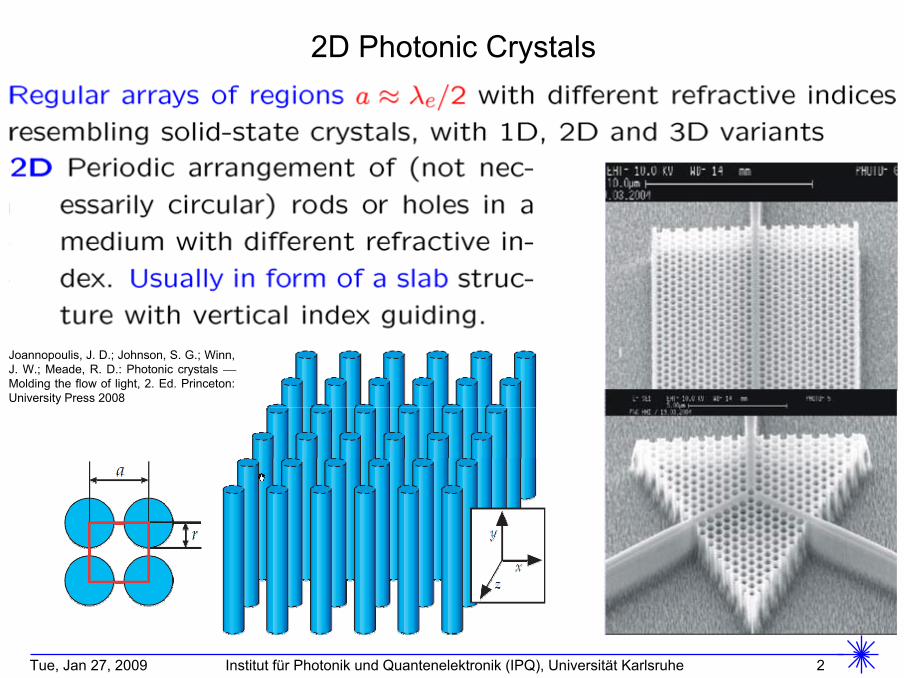
2D Photonic Crystals
Joannopoulis, J. D.; Johnson, S. G.; Winn, J. W.; Meade, R. D.: Photonic crystals
Molding
the flow of light, 2. Ed. Princeton: University Press 2008
Page 4
Tue, Jan 27, 2009 Institut für Photonik und Quantenelektronik (IPQ), Universität Karlsruhe 3
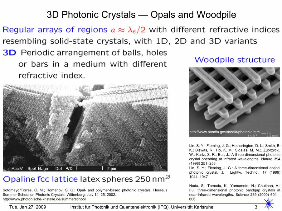
3D Photonic Crystals —
Opals and Woodpile
Lin, S. Y.; Fleming, J. G.; Hetherington, D. L.; Smith, B. K.; Biswas, R.; Ho, K. M.; Sigalas, M. M.;. Zubrzycki, W.; Kurtz, S. R.; Bur, J.: A three-dimensional photonic crystal operating at infrared wavelengths. Nature 394 (1998) 251253Lin, S. Y.; Fleming, J. G.: A three-dimensional optical photonic crystal. J. Lightw. Technol. 17 (1999) 19441947
Noda, S.; Tomoda, K.; Yamamoto, N.; Chutinan, A.: Full three-dimensional photonic bandgap
crystals at near-infrared wavelengths. Science 289 (2000) 604
606
SotomayorTorres, C. M.; Romanov, S. G.: Opal-
and polymer-based photonic crystals. Heraeus
Summer School on Photonic Crystals, Wittenberg, July 1425, 2002.
http://www.photonische-kristalle.de/summerschool
http://www.sandia.gov/media/photonic.htm
Page 5
Tue, Jan 27, 2009 Institut für Photonik und Quantenelektronik (IPQ), Universität Karlsruhe 4
3D Photonic Crystals —
Direct Laser Writing
Prof. Dr. Martin Wegener´s
group at the Institute of Applied Physics, University of Karlsruhe
http://www.aph.uni-karlsruhe.de/...…wegener/en/research/photonic-crystals
http://www.sandia.gov/media/photonic.htm
Page 6
Tue, Jan 27, 2009 Institut für Photonik und Quantenelektronik (IPQ), Universität Karlsruhe 5
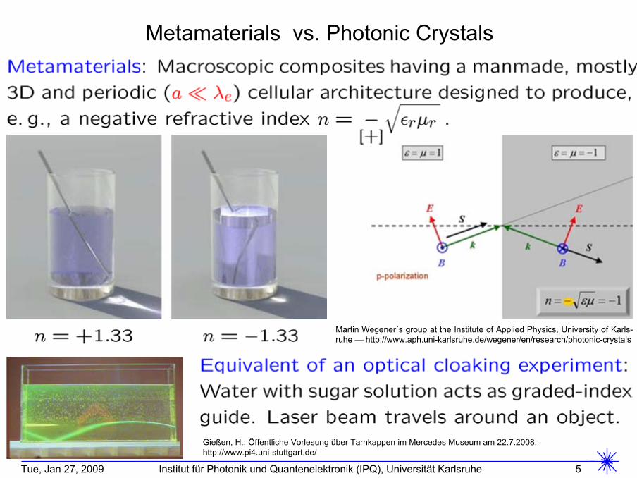
Metamaterials
vs. Photonic Crystals
Martin Wegener´s
group at the Institute of Applied Physics, University of Karls-
ruhe
http://www.aph.uni-karlsruhe.de/wegener/en/research/photonic-crystals
Gießen, H.: Öffentliche Vorlesung über Tarnkappen im Mercedes Museum am 22.7.2008.
http://www.pi4.uni-stuttgart.de/
Page 7
Tue, Jan 27, 2009 Institut für Photonik und Quantenelektronik (IPQ), Universität Karlsruhe 6
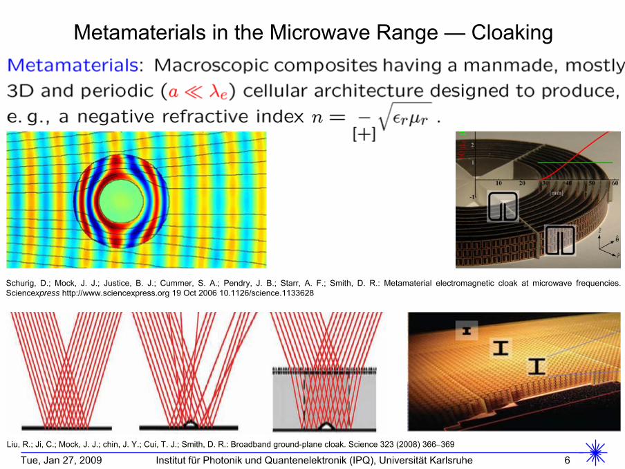
Metamaterials
in the Microwave Range —
Cloaking
Schurig, D.; Mock, J. J.; Justice, B. J.; Cummer, S. A.; Pendry, J. B.; Starr, A. F.; Smith, D. R.: Metamaterial
electromagnetic cloak at microwave frequencies. Sciencexpress http://www.sciencexpress.org
19 Oct 2006 10.1126/science.1133628
Liu, R.; Ji, C.; Mock, J. J.; chin, J. Y.; Cui, T. J.; Smith, D. R.: Broadband ground-plane cloak. Science 323 (2008) 366369
Page 8
Tue, Jan 27, 2009 Institut für Photonik und Quantenelektronik (IPQ), Universität Karlsruhe 7
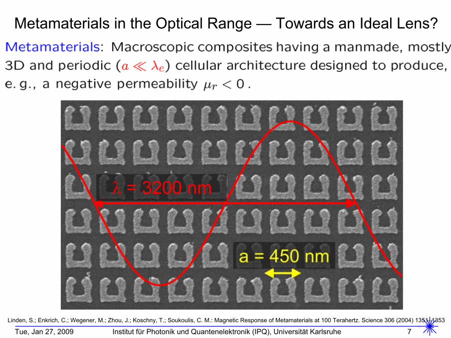
Metamaterials
in the Optical Range —
Towards an Ideal Lens?
Linden, S.; Enkrich, C.; Wegener, M.; Zhou, J.; Koschny, T.; Soukoulis, C. M.: Magnetic Response of Metamaterials
at 100 Terahertz. Science 306 (2004) 13511353
Page 9
Tue, Jan 27, 2009 Institut für Photonik und Quantenelektronik (IPQ), Universität Karlsruhe 8
•
Fundamentals of photonic crystals
Maxwell’s equations and the scaling law Bandstructure
of photonic crystals•
Applications and technology
Optical communications and silicon photonics
Slowing down light
Designing chromatic dispersion
Coupling to photonic crystals
•
Photonic crystal devices
Tunable
dispersion compensator
Tunable
delay line
Electro-optic modulator
Measurements
•
Summary
Outline
•
Fundamentals of photonic crystals
Maxwell’s equations and the scaling law
Bandstructure
of photonic crystals
Page 10
Tue, Jan 27, 2009 Institut für Photonik und Quantenelektronik (IPQ), Universität Karlsruhe 9
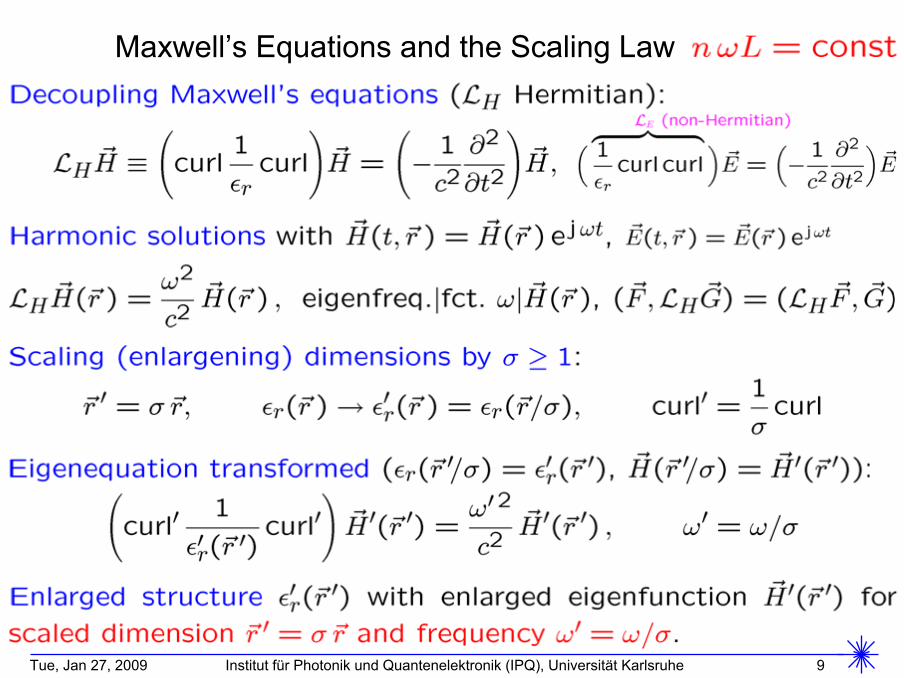
Maxwell’s Equations and the Scaling Law
Page 11
Tue, Jan 27, 2009 Institut für Photonik und Quantenelektronik (IPQ), Universität Karlsruhe 10
Microwave
Experiments
Advantages:•
Highly
precise
fabrication
(CNC),
equivalent
accuracy
0.5 nm •
Highly
accurate
measurement
equipment
with
large bandwidth•
Flexible and modular setup
Enlargement
of structure
by
= 20,000 (400 nm
8 mm)Decrease
of frequency
by
20,000 (200 THz 10 GHz)
Material:Ceramic-reinforced
PTFE (Teflon)
Refractive
index
at 10 GHz similar
as for
silicon
at 200 THz
Accurate real-time check of numerical simulations (“analogue computer”) Influence of fabrication imperfections may be investigated
Result: Simulations with finite-integration technique (FIT) and guided-
mode expansion (GME) method well suited for design
Brosi et. al., J. Lightw. Technol., vol. 25, no. 9, pp. 2502-2510, Sept. 2007
Page 12
Tue, Jan 27, 2009 Institut für Photonik und Quantenelektronik (IPQ), Universität Karlsruhe 11
•
Fundamentals of photonic crystals
Maxwell’s equations and the scaling law
Bandstructure
of photonic crystals•
Applications and technology
Optical communications and silicon photonics
Slowing down light
Designing chromatic dispersion
Coupling to photonic crystals
•
Photonic crystal devices
Tunable
dispersion compensator
Tunable
delay line
Electro-optic modulator
Measurements
•
Summary
Outline
Page 13
Tue, Jan 27, 2009 Institut für Photonik und Quantenelektronik (IPQ), Universität Karlsruhe 12
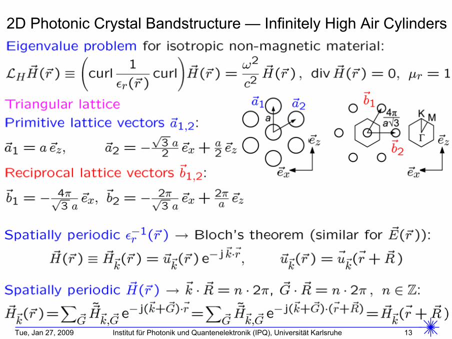
2D Photonic Crystal Bandstructure
— Infinitely High Air Cylinders
Page 14
Tue, Jan 27, 2009 Institut für Photonik und Quantenelektronik (IPQ), Universität Karlsruhe 13
2D Photonic Crystal Bandstructure
— Infinitely High Air Cylinders
Page 15
Tue, Jan 27, 2009 Institut für Photonik und Quantenelektronik (IPQ), Universität Karlsruhe 14
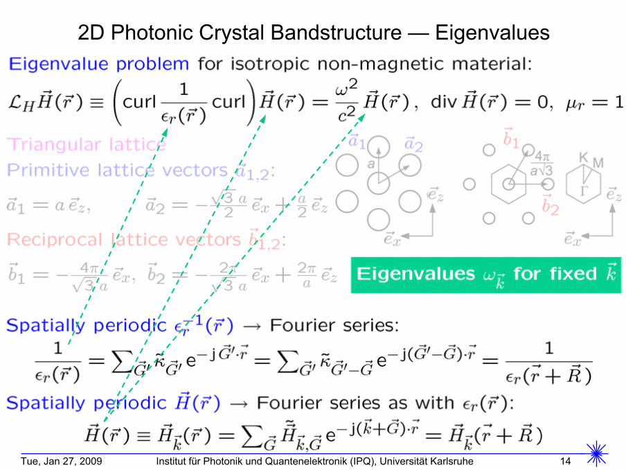
2D Photonic Crystal Bandstructure
— Eigenvalues
Page 16
Tue, Jan 27, 2009 Institut für Photonik und Quantenelektronik (IPQ), Universität Karlsruhe 15
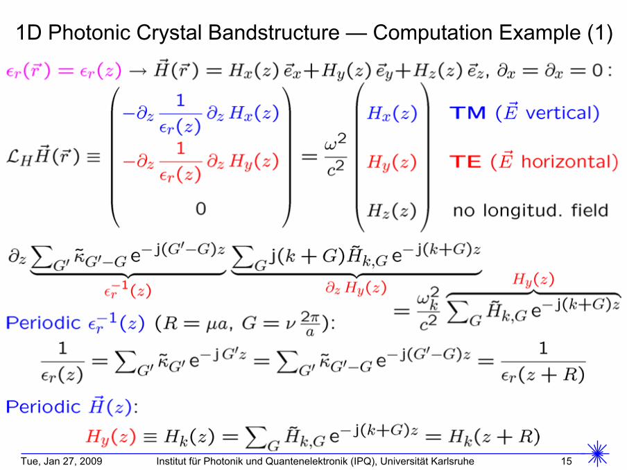
1D Photonic Crystal Bandstructure
— Computation Example (1)
Page 17
Tue, Jan 27, 2009 Institut für Photonik und Quantenelektronik (IPQ), Universität Karlsruhe 17
1D Photonic Crystal Bandstructure
— Computation Example (3)
Page 18
Tue, Jan 27, 2009 Institut für Photonik und Quantenelektronik (IPQ), Universität Karlsruhe 18
GH
z
0 –15
–30 dB –60
1D Photonic Crystal Bandstructure
— Insertion Loss
L
za
insertion
loss
in dB
Page 19
Tue, Jan 27, 2009 Institut für Photonik und Quantenelektronik (IPQ), Universität Karlsruhe 19
Joannopoulis, J. D.; Johnson, S. G.; Winn, J. W.; Meade, R. D.: Photonic crystals
Molding
the flow of light, 2. Ed. Princeton: University Press 2008 (Sect. 4 Fig. 2 p. 46)
1D Photonic Crystal Bands —
GaAs / GaAlAs
Multilayer Film
Page 20
Tue, Jan 27, 2009 Institut für Photonik und Quantenelektronik (IPQ), Universität Karlsruhe 20
1D Photonic Crystal Bands —
Group Delay at Band Edges
a
meas. phase----
linear partd ( )( ) dg
ft f t
meas. group delay
Page 21
Tue, Jan 27, 2009 Institut für Photonik und Quantenelektronik (IPQ), Universität Karlsruhe 22
2D Photonic Crystal with
Air Cylinders
— Complete
Bandstructure
TE0
0
0
5
10
15
TE
k y --
->kx --->
f / G
Hz
kz
k y
f / G
Hz
0 0
0
5
10
15
TM
k y ---
>
kx --->
f / G
Hz
TM
kz
f / G
Hz
k y
Page 22
Tue, Jan 27, 2009 Institut für Photonik und Quantenelektronik (IPQ), Universität Karlsruhe 23
•
Fundamentals of photonic crystals
Maxwell’s equations and the scaling law Bandstructure
of photonic crystals•
Applications and technology
Optical communications and silicon photonics
Slowing down light
Designing chromatic dispersion
Coupling to photonic crystals
•
Photonic crystal devices
Tunable
dispersion compensator
Tunable
delay line
Electro-optic modulator
Measurements
•
Summary
Outline
Page 23
Tue, Jan 27, 2009 Institut für Photonik und Quantenelektronik (IPQ), Universität Karlsruhe 24
High-Bitrate
Optical
Transmission and Signal Processing
lasermodu- lator
line amplifier dispersion compensator receiver
line
•
Laser: Optical
carrier
at = 1.55 µm•
Modulator: Transfers signals
on optical
carrier
(10 Gbit/s …100 Gbit/s)•
Line: Attenuation
and positive dispersion
dispersion
(= frequency-dependent
group
velocity) impulse
broadening•
Amplifier•
Dispersion compensator (DC): Negative dispersion
impulse
shortening•
Optical cross-connect (OCX): Aggregation
& grooming
(requires
delay), switching
Goals:
Modulator, DC, delay with
high functionality
and low
price
Silicon chips
fabricated
with
CMOS technology
Possible
combination
of optics
and electronics
Page 24
Tue, Jan 27, 2009 Institut für Photonik und Quantenelektronik (IPQ), Universität Karlsruhe 25
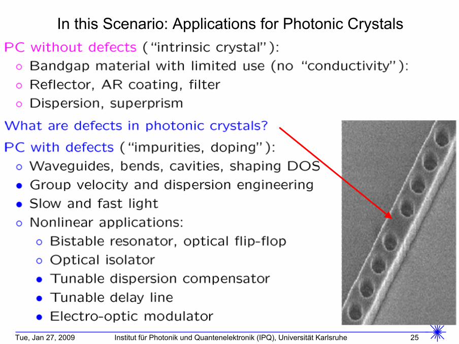
In this Scenario: Applications for Photonic Crystals
Page 25
Tue, Jan 27, 2009 Institut für Photonik und Quantenelektronik (IPQ), Universität Karlsruhe 26
2D Photonic Crystals with Defects
Page 26
Tue, Jan 27, 2009 Institut für Photonik und Quantenelektronik (IPQ), Universität Karlsruhe 27
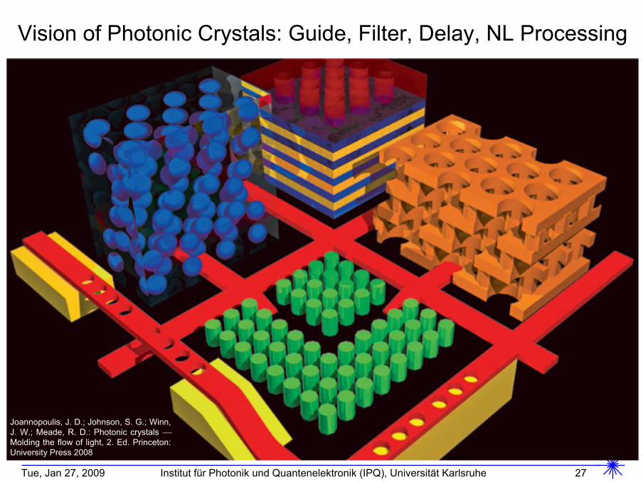
Vision of Photonic Crystals: Guide, Filter, Delay, NL Processing
Joannopoulis, J. D.; Johnson, S. G.; Winn, J. W.; Meade, R. D.: Photonic crystals
Molding
the flow of light, 2. Ed. Princeton: University Press 2008
Page 27
Tue, Jan 27, 2009 Institut für Photonik und Quantenelektronik (IPQ), Universität Karlsruhe 28
Photonic Crystals and Silicon Photonics
Silicon-on-insulator (SOI) systems promise:•
Full integration
of
electronic and optical
components•
Low-cost
CMOS-based technology•
Fabrication of ultra-compact and ultra-fast
optical devices•
Electronically powered light sources so far only in hybrid integration•
Fabrication of active
and
passive optical
components.Wafer-BondedIII-V Laser
High-Speed Electro-optical Modulator
CMOS Drivers
Photodetectorwith Built-inFilter
InputSignal
OutputSignal
Silicon-Wire-Waveguide
Page 28
Tue, Jan 27, 2009 Institut für Photonik und Quantenelektronik (IPQ), Universität Karlsruhe 29
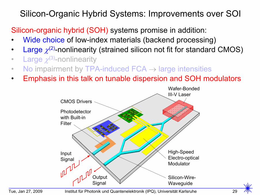
Silicon-Organic Hybrid Systems: Improvements over SOI
Silicon-organic hybrid (SOH)
systems promise in addition:•
Wide choice
of low-index materials (backend processing)•
Large (2)-nonlinearity (strained silicon not fit for standard CMOS)•
Large (3)-nonlinearity•
No
impairment by TPA-induced FCA
large intensities•
Emphasis in this talk on tunable dispersion and SOH modulatorsWafer-BondedIII-V Laser
High-Speed Electro-optical Modulator
CMOS Drivers
Photodetectorwith Built-inFilter
InputSignal
OutputSignal
Silicon-Wire-Waveguide
Page 29
Tue, Jan 27, 2009 Institut für Photonik und Quantenelektronik (IPQ), Universität Karlsruhe 30
Photonic Crystals in SOI
Dielectric transparent material (silicon) with periodic structure Bragg
reflexion, if
e
/ 2
a No light propagation
for
certain
frequencies
photonic
bandgap
Introducing defects (impurities, doping) Light propagation
along
defects Slow
group
velocity
vg
(slow
light) and large dispersion
vg
(f) Designing
vg
(f) by
structural
changes
Applications for tailored dispersion:•
Large negative chromatic
dispersion, e.g., for
dispersion
compensation•
Slow
light for
optical
delay, e.g., for
aggregation
in OXC•
Slow
light for
increased
light-matter
interaction, e.g., for
modulation
Page 30
Tue, Jan 27, 2009 Institut für Photonik und Quantenelektronik (IPQ), Universität Karlsruhe 31
Fabrication
Technologies
Structure roughness: Main source of losses• Losses
increase
for
small
group
velocities
vg
• Losses
limit
the
lowest
usable
vg
Numerical investigations of roughness loss• Air hole positions
regular• Radii
with
normal distribution, r = 5 nm
Design goal: Minimum loss
siliconglass
air
symmetric in air membrane
structuresymmetric in glass buried
structureunsymmetric silicon-on-insulator
(SOI)
Comparison of different structures: Broadband
slow
light with
vg / c = 4 %
Variation of defect
(WG) width, mode number
and height
of silicon
layer
(220 nm)
glass
Page 31
Tue, Jan 27, 2009 Institut für Photonik und Quantenelektronik (IPQ), Universität Karlsruhe 32
•
Fundamentals of photonic crystals
Maxwell’s equations and the scaling law Bandstructure
of photonic crystals•
Applications and technology
Optical communications and silicon photonics
Slowing down light
Designing chromatic dispersion
Coupling to photonic crystals
•
Photonic crystal devices
Tunable
dispersion compensator
Tunable
delay line
Electro-optic modulator
Measurements
•
Summary
Outline
Page 32
Tue, Jan 27, 2009 Institut für Photonik und Quantenelektronik (IPQ), Universität Karlsruhe 33
Slow
Light in Photonic
a Crystal (1)
Without crystal defects: Photonic bandgap
TE polarisation:
Dominant electric
field
Ex
Ex
Parameterh Waveguide
height
~ 220 nmr Radii
of air holes
~ 120 nma Lattice
constant
of PC ~ 400 nm
c Vacuum
speed
of lightk Propagation
constant
in z-direction0.0 0.2 0.4 0.6 0.8 1.0
0.25
0.30
0.35
Lichtlinie
Freq
uenz
f a
/ c
Ausbreitungskonstante k a /
Page 33
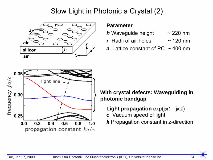
Tue, Jan 27, 2009 Institut für Photonik und Quantenelektronik (IPQ), Universität Karlsruhe 34
Slow
Light in Photonic
a Crystal (2)
Light propagation exp(jt – jkz) c Vacuum
speed
of lightk Propagation
constant
in z-direction
With crystal defects: Waveguiding in photonic bandgap
0.0 0.2 0.4 0.6 0.8 1.00.25
0.30
0.35Lichtlinie
Freq
uenz
f a
/ c
Ausbreitungskonstante k a /
Parameterh Waveguide
height
~ 220 nmr Radii
of air holes
~ 120 nma Lattice
constant
of PC ~ 400 nm
Page 34
Tue, Jan 27, 2009 Institut für Photonik und Quantenelektronik (IPQ), Universität Karlsruhe 35
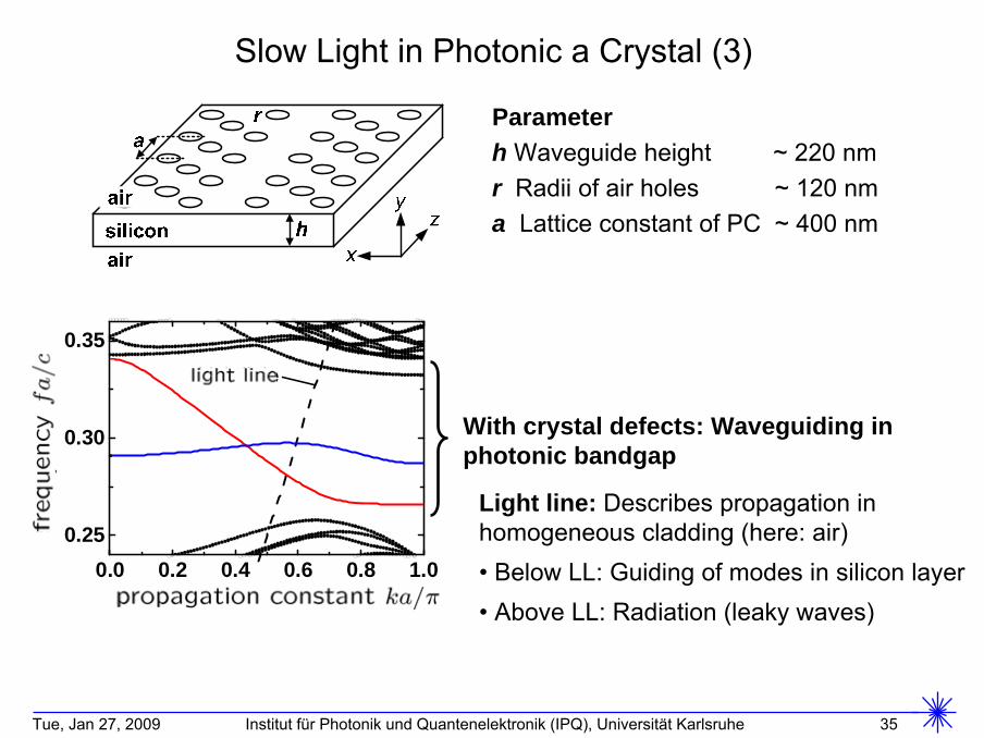
Slow
Light in Photonic
a Crystal (3)
With crystal defects: Waveguiding in photonic bandgap
Light line: Describes
propagation
in homogeneous
cladding
(here: air)• Below
LL: Guiding
of modes
in silicon
layer• Above
LL: Radiation
(leaky
waves)
0.0 0.2 0.4 0.6 0.8 1.00.25
0.30
0.35Lichtlinie
Freq
uenz
f a
/ c
Ausbreitungskonstante k a /
Parameterh Waveguide
height
~ 220 nmr Radii
of air holes
~ 120 nma Lattice
constant
of PC ~ 400 nm
Page 35
Tue, Jan 27, 2009 Institut für Photonik und Quantenelektronik (IPQ), Universität Karlsruhe 36
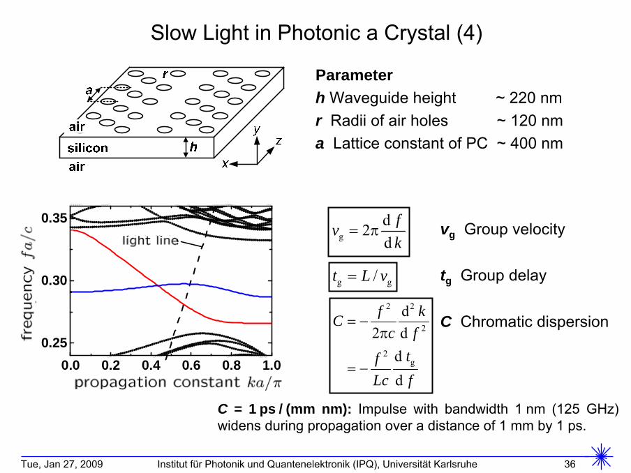
Slow
Light in Photonic
a Crystal (4)
tg Group delayg g/t L v
C Chromatic
dispersion2 2
2
2g
d2 d
d d
f kCc f
tfLc f
gd2d
fvk
vg Group velocity
C = 1 ps / (mm nm): Impulse with
bandwidth
1
nm (125 GHz) widens
during
propagation
over
a distance of 1 mm by
1 ps.
0.0 0.2 0.4 0.6 0.8 1.00.25
0.30
0.35Lichtlinie
Freq
uenz
f a
/ c
Ausbreitungskonstante k a /
Parameterh Waveguide
height
~ 220 nmr Radii
of air holes
~ 120 nma Lattice
constant
of PC ~ 400 nm
Page 36
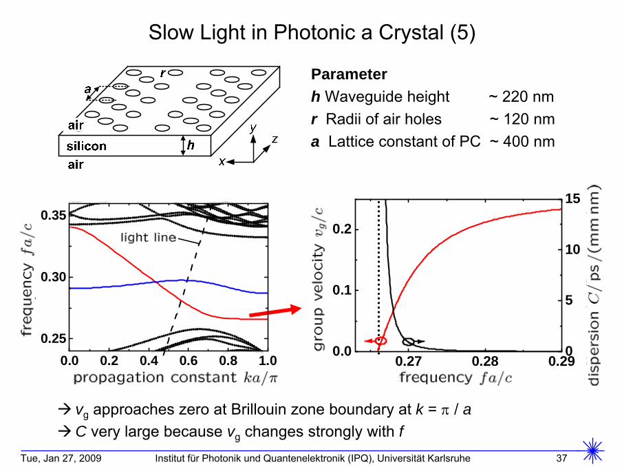
Tue, Jan 27, 2009 Institut für Photonik und Quantenelektronik (IPQ), Universität Karlsruhe 37
Slow
Light in Photonic
a Crystal (5)
vg
approaches
zero
at Brillouin zone
boundary
at k =
/ aC very
large because
vg
changes
strongly
with
f
0.0 0.2 0.4 0.6 0.8 1.00.25
0.30
0.35Lichtlinie
Freq
uenz
f a
/ c
Ausbreitungskonstante k a /
Parameterh Waveguide
height
~ 220 nmr Radii
of air holes
~ 120 nma Lattice
constant
of PC ~ 400 nm
0.27 0.28 0.290.0
0.1
0.2
0
5
10
15
Gru
ppen
gesc
hw. v
g / c
Frequenz f a / c
Dispersion C
[ps/(mm
nm)]
Page 37
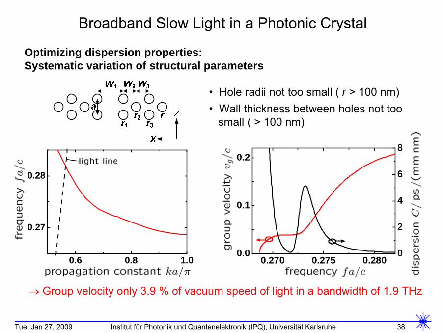
Tue, Jan 27, 2009 Institut für Photonik und Quantenelektronik (IPQ), Universität Karlsruhe 38
Broadband
Slow
Light in a Photonic
Crystal
Optimizing dispersion properties: Systematic variation of structural parameters
• Hole radii
not too
small
( r > 100 nm)•
Wall thickness
between
holes
not too
small
( > 100 nm)
Group velocity
only
3.9 % of vacuum
speed
of light in a bandwidth
of 1.9 THz
0.6 0.8 1.0
0.27
0.28Lichtlinie
Freq
uenz
f a
/ c
Ausbreitungskonstante k a / 0.270 0.275 0.280
0.0
0.1
0.2
0
2
4
6
8
Gru
ppen
gesc
hw. v
g / c
Frequenz f a / c
Dispersion C
[ps/(mm
nm)]
Page 38
Tue, Jan 27, 2009 Institut für Photonik und Quantenelektronik (IPQ), Universität Karlsruhe 39
•
Fundamentals of photonic crystals
Maxwell’s equations and the scaling law Bandstructure
of photonic crystals•
Applications and technology
Optical communications and silicon photonics
Slowing down light
Designing chromatic dispersion
Coupling to photonic crystals
•
Photonic crystal devices
Tunable
dispersion compensator
Tunable
delay line
Electro-optic modulator
Measurements
•
Summary
Outline
Page 39
Tue, Jan 27, 2009 Institut für Photonik und Quantenelektronik (IPQ), Universität Karlsruhe 40
Negative chromatic
dispersion
of 4.5
ps /
(mm nm) and regions
with
linear dispersion
Negative Chromatic
Dispersion
0.6 0.8 1.0
0.27
0.28Lichtline
Freq
uenz
f a
/ c
Ausbreitungskonstante k a /
Optimizing dispersion properties: Systematic variation of structural parameters
• Hole radii
not too
small
( r > 100 nm)•
Wall thickness
between
holes
not too
small
( > 100 nm)
0.270 0.275 0.280
0.0
0.1
0.2
-5
0
5
10
15
Gru
ppen
gesc
hw. v
g / c
Frequenz f a / c
Dispersion C
[ps/(mm
nm)]
Page 40
Tue, Jan 27, 2009 Institut für Photonik und Quantenelektronik (IPQ), Universität Karlsruhe 41
•
Fundamentals of photonic crystals
Maxwell’s equations and the scaling law Bandstructure
of photonic crystals•
Applications and technology
Optical communications and silicon photonics
Slowing down light
Designing chromatic dispersion
Coupling to photonic crystals
•
Photonic crystal devices
Tunable
dispersion compensator
Tunable
delay line
Electro-optic modulator
Measurements
•
Summary
Outline
Page 41
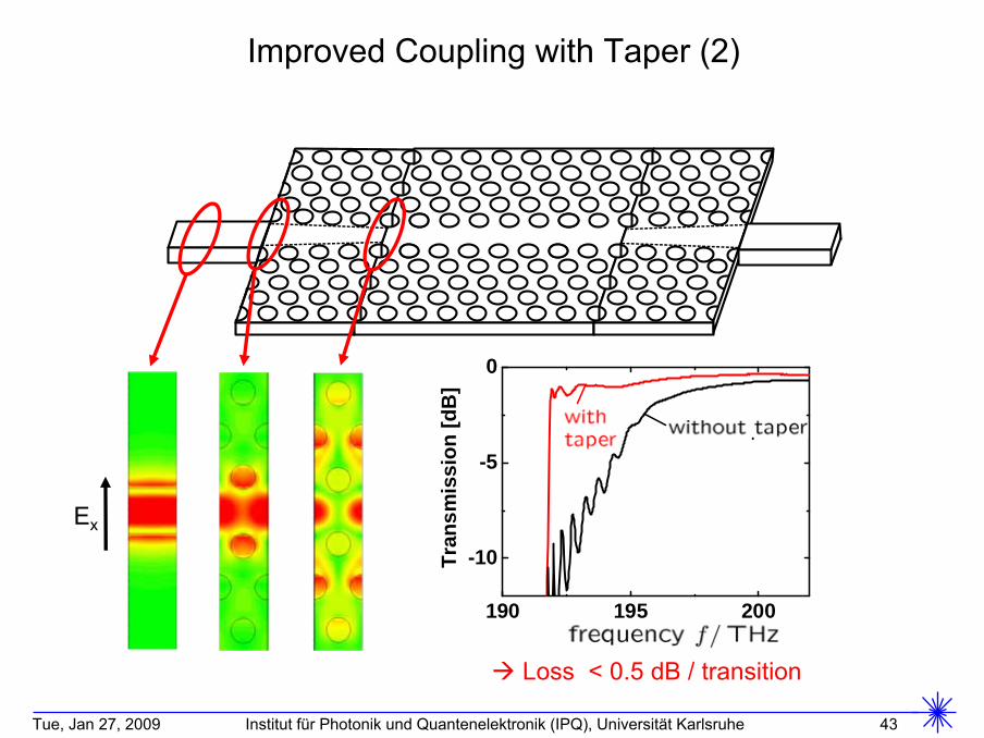
Tue, Jan 27, 2009 Institut für Photonik und Quantenelektronik (IPQ), Universität Karlsruhe 42
Improved
Coupling
with
Taper
(1)
Taper: Slight
continuous
structural
change
strip
waveguide
slow-light
waveguide
Page 42
Tue, Jan 27, 2009 Institut für Photonik und Quantenelektronik (IPQ), Universität Karlsruhe 43
Improved
Coupling
with
Taper
(2)
Ex
190 195 200
-10
-5
0
Tran
smis
sion
[dB
]
Frequenz f [THz]
MitTaper Ohne Taper
Loss
< 0.5 dB / transition
Page 43
Tue, Jan 27, 2009 Institut für Photonik und Quantenelektronik (IPQ), Universität Karlsruhe 44
•
Fundamentals of photonic crystals
Maxwell’s equations and the scaling law Bandstructure
of photonic crystals•
Applications and technology
Optical communications and silicon photonics
Slowing down light
Designing chromatic dispersion
Coupling to photonic crystals
•
Photonic crystal devices
Tunable
dispersion compensator
Tunable
delay line
Electro-optic modulator
Measurements
•
Summary
Outline
Page 44
Tue, Jan 27, 2009 Institut für Photonik und Quantenelektronik (IPQ), Universität Karlsruhe 45
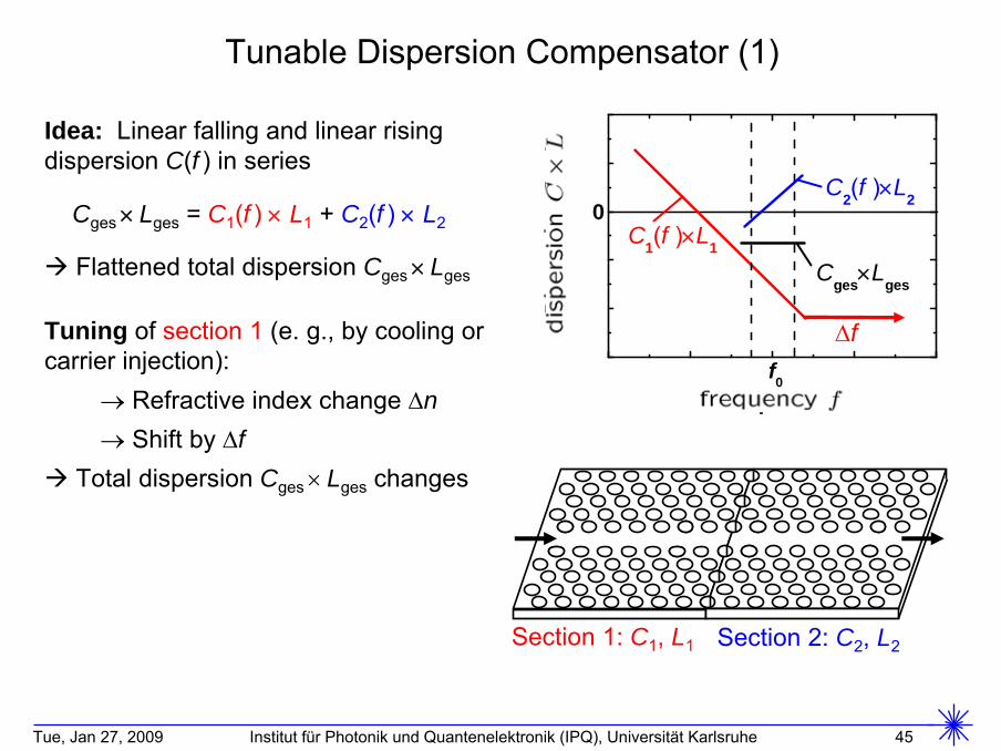
Tunable
Dispersion Compensator
(1)
0C2(f )L2
CgesLges
C1(f )L1
Dis
pers
ion
C
L
Frequenz ff0
Idea: Linear falling
and linear rising
dispersion
C(f ) in series
Cges
Lges
= C1
(f )
L1
+ C2
(f )
L2
Flattened
total dispersion
Cges
Lges
Tuning of section
1
(e. g., by
cooling
or
carrier
injection): Refractive
index
change
n Shift
by
f Total dispersion
Cges
Lges
changes
f
Section
1: C1
, L1 Section
2: C2
, L2
Page 45
Tue, Jan 27, 2009 Institut für Photonik und Quantenelektronik (IPQ), Universität Karlsruhe 46
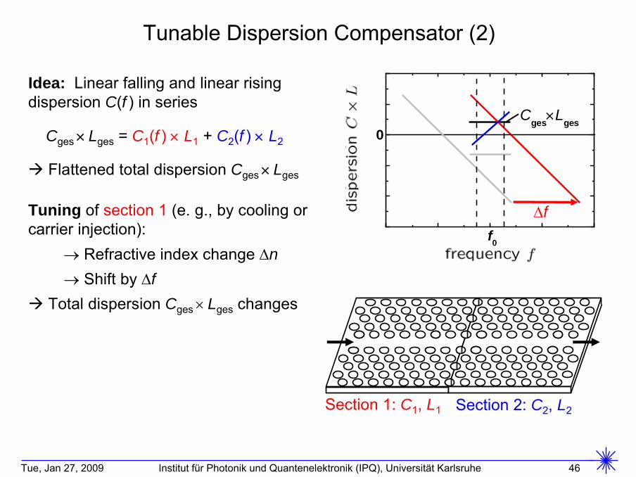
Tunable
Dispersion Compensator
(2)
f
Section
1: C1
, L1 Section
2: C2
, L2
0CgesLges
Dis
pers
ion
C
L
Frequenz ff0
Idea: Linear falling
and linear rising
dispersion
C(f ) in series
Cges
Lges
= C1
(f )
L1
+ C2
(f )
L2
Flattened
total dispersion
Cges
Lges
Tuning of section
1
(e. g., by
cooling
or
carrier
injection): Refractive
index
change
n Shift
by
f Total dispersion
Cges
Lges
changes
Page 46
Tue, Jan 27, 2009 Institut für Photonik und Quantenelektronik (IPQ), Universität Karlsruhe 47
Tunable
Dispersion Compensator
(3)
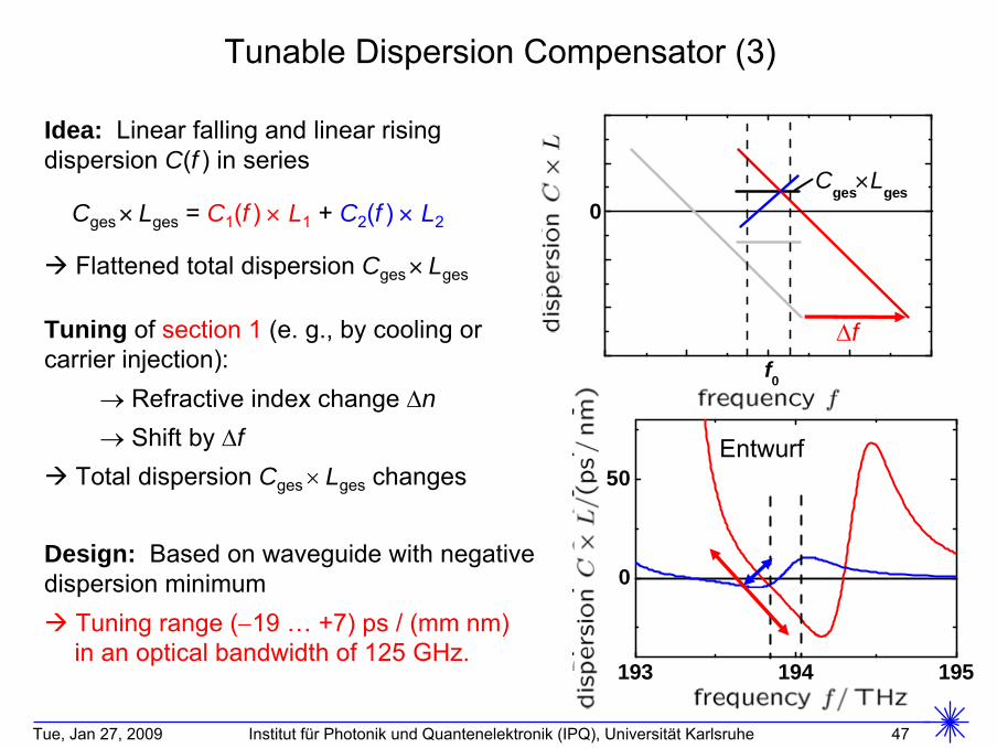
Idea: Linear falling
and linear rising
dispersion
C(f ) in series
Cges
Lges
= C1
(f )
L1
+ C2
(f )
L2
Flattened
total dispersion
Cges
Lges
Tuning of section
1
(e. g., by
cooling
or
carrier
injection): Refractive
index
change
n Shift
by
f Total dispersion
Cges
Lges
changes
Design: Based
on waveguide
with
negative dispersion
minimum Tuning range
(19 …
+7) ps / (mm nm) in an optical
bandwidth
of 125 GHz.
f
0CgesLges
Dis
pers
ion
C
L
Frequenz ff0
193 194 195
0
50
Dis
pers
ion
C x
L [p
s / n
m]
Frequenz f [THz]
Entwurf
Page 47
Tue, Jan 27, 2009 Institut für Photonik und Quantenelektronik (IPQ), Universität Karlsruhe 48
•
Fundamentals of photonic crystals
Maxwell’s equations and the scaling law Bandstructure
of photonic crystals•
Applications and technology
Optical communications and silicon photonics
Slowing down light
Designing chromatic dispersion
Coupling to photonic crystals
•
Photonic crystal devices
Tunable
dispersion compensator
Tunable
delay line
Electro-optic modulator
Measurements
•
Summary
Outline
Page 48
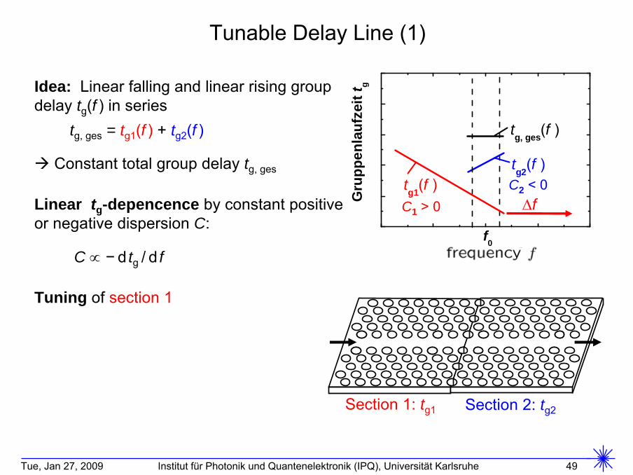
Tue, Jan 27, 2009 Institut für Photonik und Quantenelektronik (IPQ), Universität Karlsruhe 49
Tunable
Delay
Line (1)
tg, ges(f )
tg1(f )tg2(f )
Gru
ppen
lauf
zeit
t g
Frequenz ff0
Idea: Linear falling
and linear rising
group
delay
tg
(f ) in seriestg, ges
= tg1
(f )
+ tg2
(f )
Constant
total group
delay
tg, ges
Linear tg -depencence by
constant
positive or
negative dispersion
C:
C
−
d tg
/ d f
Tuning of section
1
C1 > 0C2 < 0f
Section
1: tg1 Section
2: tg2
Page 49
Tue, Jan 27, 2009 Institut für Photonik und Quantenelektronik (IPQ), Universität Karlsruhe 50
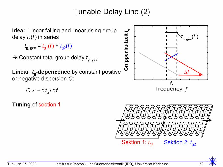
tg, ges(f )
Gru
ppen
lauf
zeit
t g
Frequenz ff0
Tunable
Delay
Line (2)
f
Sektion 1: tg1 Sektion 2: tg2
Idea: Linear falling
and linear rising
group
delay
tg
(f ) in seriestg, ges
= tg1
(f )
+ tg2
(f )
Constant
total group
delay
tg, ges
Linear tg -depencence by
constant
positive or
negative dispersion
C:
C
−
d tg
/ d f
Tuning of section
1
Page 50
Tue, Jan 27, 2009 Institut für Photonik und Quantenelektronik (IPQ), Universität Karlsruhe 51
Tunable
Delay
Line (3)
Idea: Linear falling
and linear rising
group
delay
tg
(f ) in seriestg, ges
= tg1
(f )
+ tg2
(f )
Constant
total group
delay
tg, ges
Linear tg -depencence by
constant
positive or
negative dispersion
C:
C
−
d tg
/ d f
Tuning of section
1
Total group
delay
tg, tot
changes.
Design: Tuning range
42 ps (1.7 bit
at 40 Gbit/s)
in an optical
bandwidth
of 125 GHz
for
a length
of 1 mm. 192 193 194 1950
50
Gru
ppen
lauf
zeit
t g c
/ L
Frequenz f [THz]
f
Entwurf
tg, ges(f )
Gru
ppen
lauf
zeit
t g
Frequenz ff0
Page 51
Tue, Jan 27, 2009 Institut für Photonik und Quantenelektronik (IPQ), Universität Karlsruhe 52
•
Fundamentals of photonic crystals
Maxwell’s equations and the scaling law Bandstructure
of photonic crystals•
Applications and technology
Optical communications and silicon photonics
Slowing down light
Designing chromatic dispersion
Coupling to photonic crystals
•
Photonic crystal devices
Tunable
dispersion compensator
Tunable
delay line
Electro-optic modulator
Measurements
•
Summary
Outline
Page 52
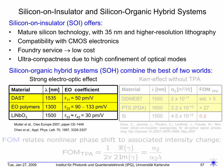
Tue, Jan 27, 2009 Institut für Photonik und Quantenelektronik (IPQ), Universität Karlsruhe 57
Silicon-on-insulator issues:• No natural electro-optic effect in silicon
o
Strained silicon breaks up inversion symmetry• Free-carrier absorption measures needed to remove carriers• (3)
in silicon is reasonably large, yet impaired by TPA-induced FCA
Material λ
[nm] EO coefficientDAST 1535 r11 = 50 pm/V
EO polymers 1300 r33 = 90 –
133 pm/V
LiNbO3 1500 r33 ≈
r42 = 30 pm/V
Material λ
[nm] n2 [m2/W] FOM TPA
DDMEBT 1500 2 x 10-17 est. > 5
PTS (PDA) 1600 2.2 x 10⁻¹⁶ > 27Si 1500 4.5 x 10⁻¹⁸ 0.3
Silicon-on-Insulator and Silicon-Organic Hybrid Systems
Strong
electro-optic
effect
Mutter et al., Cleo Europe 2007, paper CE-1449
Chen et al., Appl. Phys. Lett. 70, 1997, 3335-3337
Koos, C.; Jacome, L.; Poulton, C.; Leuthold, J.; Freude, W.: Non-
linear silicon-on-insulator waveguides for all-optical signal proces-
sing. Opt. Express 15 (2007) 5976–5990, May 2007
Kerr-effect
without
TPASilicon-organic hybrid systems (SOH) combine the best of two worlds:
Silicon-on-insulator (SOI) offers:•
Mature silicon technology, with 35 nm and higher-resolution lithography•
Compatibility with CMOS electronics•
Foundry service low cost•
Ultra-compactness due to high confinement of optical modes
Page 53
Tue, Jan 27, 2009 Institut für Photonik und Quantenelektronik (IPQ), Universität Karlsruhe 58
SOH MZ-Modulator with
Slow-Light
Photonic
Crystal Slot
WG
J.-M. Brosi, C. Koos, L. C. Andreani, M. Waldow, J. Leuthold, W. Freude: High-
speed low-voltage electro-optic modulator with a polymer-infiltrated silicon
photonic crystal waveguide, Opt. Express, vol. 16, pp.
41774191, March 2008
Page 54
Tue, Jan 27, 2009 Institut für Photonik und Quantenelektronik (IPQ), Universität Karlsruhe 59
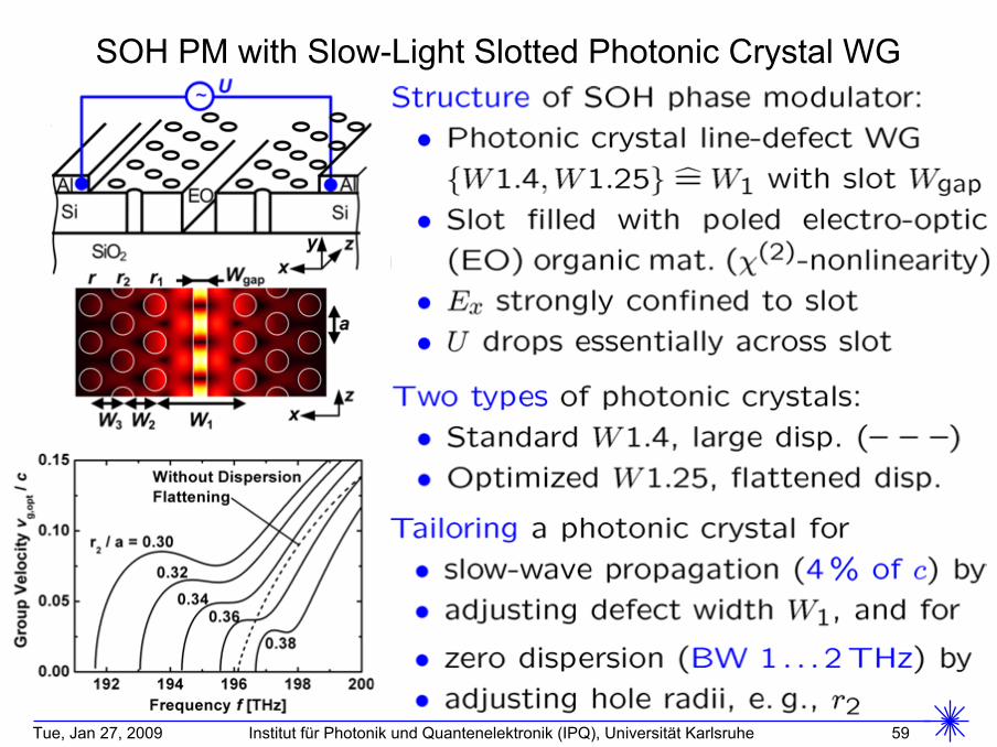
SOH PM with
Slow-Light
Slotted
Photonic
Crystal WG
Page 55
Tue, Jan 27, 2009 Institut für Photonik und Quantenelektronik (IPQ), Universität Karlsruhe 60
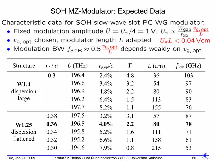
SOH MZ-Modulator: Expected
Data
Structure r2 / a fo (THz) vg,opt/c Г L (m) f3dB (GHz) 0.3 196.4 2.4% 4.8 36 103
196.6 3.4% 3.2 54 97 196.9 4.8% 2.2 80 90 196.2 6.4% 1.5 113 83
W1.4 dispersion
large 197.7 8.2% 1.1 155 76
0.38 197.5 3.2% 3.1 57 87 0.36 196.5 4.0% 2.2 80 78 0.34 195.8 5.2% 1.6 111 71 0.32 195.2 6.6% 1.1 158 61
W1.25 dispersion flattened
0.30 194.6 7.9% 0.8 215 53
Page 56
Tue, Jan 27, 2009 Institut für Photonik und Quantenelektronik (IPQ), Universität Karlsruhe 61
Taper for Broadband Low Dispersion Slow Light PC Slot-WG
Page 57
Tue, Jan 27, 2009 Institut für Photonik und Quantenelektronik (IPQ), Universität Karlsruhe 62
Fabrication
of SOH Phase (and MZ) Modulator with
PC Taper
Page 58
Tue, Jan 27, 2009 Institut für Photonik und Quantenelektronik (IPQ), Universität Karlsruhe 63
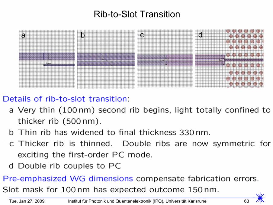
Rib-to-Slot Transition
a b c d
Page 59
Tue, Jan 27, 2009 Institut für Photonik und Quantenelektronik (IPQ), Universität Karlsruhe 64
Two Slow-Light Photonic Crystal Families
varying radii identical radii, shifted position
J. Li, T. P. White, L. O`Faolain, A. Gomez-Iglesias, T. F. Krauss:
Systematic design of flat and slow light in photonic crystal waveguide. Opt. Express, vol. 16, pp. 62276232, April 2008
J.-M. Brosi, C. Koos, L. C. Andreani, M. Waldow, J. Leuthold, W.
Freude: High-speed low-voltage electro-optic modulator with a polymer-
infiltrated silicon photonic crystal waveguide, Opt. Express, vol. 16, pp.
41774191, March 2008
Page 60
Tue, Jan 27, 2009 Institut für Photonik und Quantenelektronik (IPQ), Universität Karlsruhe 67
•
Fundamentals of photonic crystals
Maxwell’s equations and the scaling law Bandstructure
of photonic crystals•
Applications and technology
Optical communications and silicon photonics
Slowing down light
Designing chromatic dispersion
Coupling to photonic crystals
•
Photonic crystal devices
Tunable
dispersion compensator
Tunable
delay line
Electro-optic modulator
Measurements
•
Summary
Outline
Page 61
Tue, Jan 27, 2009 Institut für Photonik und Quantenelektronik (IPQ), Universität Karlsruhe 68
Broadband Slow Light PC WG with Low Dispersion
Brosi, J.-M.; Koos, C.; Andreani, L. C.: Dumon, P.; Baets, R.; Leuthold, J.; Freude, W.: '100 Gbit/s / 1 V optical modulator with slotted slow-light polymer-
infiltrated silicon photonic crystal', OSA Topical Meeting on Slow and Fast Light (SL'08), Boston (MA), USA, 13–16 July 2008. Paper SWC3
Page 62
Tue, Jan 27, 2009 Institut für Photonik und Quantenelektronik (IPQ), Universität Karlsruhe 69
•
Fundamentals of photonic crystals
Maxwell’s equations and the scaling law Bandstructure
of photonic crystals•
Applications and technology
Optical communications and silicon photonics
Slowing down light
Designing chromatic dispersion
Coupling to photonic crystals
•
Photonic crystal devices
Tunable
dispersion compensator
Tunable
delay line
Electro-optic modulator
Measurements
•
Summary
Outline
Page 63
Tue, Jan 27, 2009 Institut für Photonik und Quantenelektronik (IPQ), Universität Karlsruhe 70
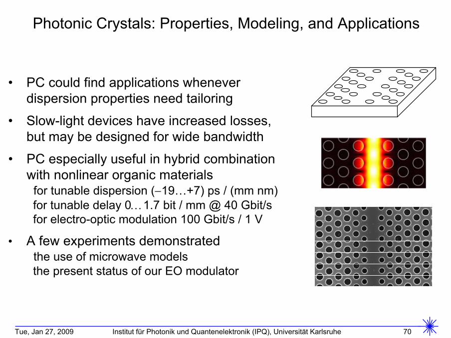
Photonic Crystals: Properties, Modeling, and Applications
•
PC could
find applications
whenever
dispersion
properties
need
tailoring
•
Slow-light
devices
have
increased
losses,
but
may
be
designed
for
wide
bandwidth
•
PC especially
useful
in hybrid combination
with
nonlinear
organic
materials
for
tunable
dispersion
(19…+7) ps / (mm nm)
for
tunable
delay
01.7 bit
/ mm @ 40 Gbit/s
for
electro-optic
modulation
100 Gbit/s / 1 V
•
A few
experiments
demonstrated
the
use
of microwave
models
the
present
status
of our
EO modulator
Page 64
Tue, Jan 27, 2009 Institut für Photonik und Quantenelektronik (IPQ), Universität Karlsruhe 71
Further
Reading
(1/2)
Page 65
Tue, Jan 27, 2009 Institut für Photonik und Quantenelektronik (IPQ), Universität Karlsruhe 72
Further
Reading
(2/2)