1 Telecommunication Engineering group University of Twente, Enschede, The Netherlands International Workshop on Phased Array Antenna Systems for Radio Astronomy May 3-5, 2010 Design Optimization of Phased Arrays and RF Electronics Photonic Integrated Beamformer for Broadband Radio Astronomy A. Leinse, M. Hoekman, R. G. Heideman LioniX BV, Enschede, The Netherlands M. Burla , D. A. I. Marpaung, M. R. H. Khan, C. G. H. Roeloffzen P. Maat, K. Dijkstra ASTRON, Dwingeloo, The Netherlands
Transcript
1
Telecommunication Engineering group University of Twente, Enschede, The Netherlands
International Workshop on Phased Array Antenna Systems
for Radio AstronomyMay 3-5, 2010
Design Optimization of Phased Arrays and RF Electronics
Photonic Integrated Beamformer for Broadband Radio Astronomy
A. Leinse, M. Hoekman, R. G. Heideman LioniX BV, Enschede, The Netherlands
M. Burla, D. A. I. Marpaung, M. R. H. Khan, C. G. H. Roeloffzen
P. Maat, K. Dijkstra ASTRON, Dwingeloo, The Netherlands
2
Introduction
Photonic integrated beamformers- fields of application- RF-to-RF characterization- demonstration of broadband beamsteering
Integration
New architectures
Conclusions
Outline
3Telecommunication Engineering Group
• 6 scientific staff• 4 postdoctoral researchers• 12 PhD students• 6 MSc and BSc students
Requirements: Broadband High-resolution, squint-free architecture Continuously tunable beam direction
Applications for optical beamforming
6
RF-to-RF characterization of a phased array antenna using an integrated OBFN
From
“RF-to-RF Characterization of a Phased Array Receive Antenna Steering System Using a Novel Ring Resonator-Based Integrated Photonic Beamformer”, L. Zhuang, M. Burla, C. G. H. Roeloffzen, A.
Meijerink, D. A. I. Marpaung, M. R. H. Khan, W. van Etten, A. Leinse, M. Hoekman, R. G. Heideman
Presented at the 2009 International Topical Meeting on MICROWAVE PHOTONICS, Valencia, Spain, 14-16 Oct. 2009. (Microwave Photonic Techniques for Antennas)
7
Beam forming network: Delay on
Phased array antenna: principle of operation
• Broadband phased antenna arrays require true time delays• Not easy to be realized over a broad band• Photonic technology can help…
Requirements
RF-to-RF characterization
8
0,0
-7,0
-6,0
-5,0
-4,0
-3,0
-2,0
-1,0
10230 100 200 300 400 500 600 700 800 900
Phase Output (lin scale)
ORR
Ideal delay line
L
• Optical delay generation: implemented using optical resonators
• Comparison of an Optical Ring Resonator (ORR) with an ideal delay line:
0,0
-7,0
-6,0
-5,0
-4,0
-3,0
-2,0
-1,0
10230 100 200 300 400 500 600 700 800 900
Phase Output (lin scale)
FSR
RF-to-RF characterization
f
9
Optical delay generation
T41
− 0T41
T21
T21
−
T8
T4
T2
T6
T10
0→ f
Group delay
TFSR 1
=
Optical ring resonator:
T : Round trip time
κ : Power coupling coefficient
φ : Additional phase
φ
κ
T π2−
0
π2.1−
π6.1−
π8.0−
π4.0−
Phase
Trade-off: delay vs bandwidth
RF-to-RF characterization
10
Optical delay generation
Enhanced bandwidth Trade-off: delay vs. bandwidth vs. delay ripple vs. no. rings
ripple
bandwidth
T41
− 0T41
T21
T21
−
→ f
T8
T4
T2
T6
0
→G
roup
del
ay
T10
T41
− 0T41
T21
T21
−
→ f
Cascaded ring resonators:
DesignRequired delay
Required BW
Least number of rings
Max ripple
Design procedure:
RF-to-RF characterization
11
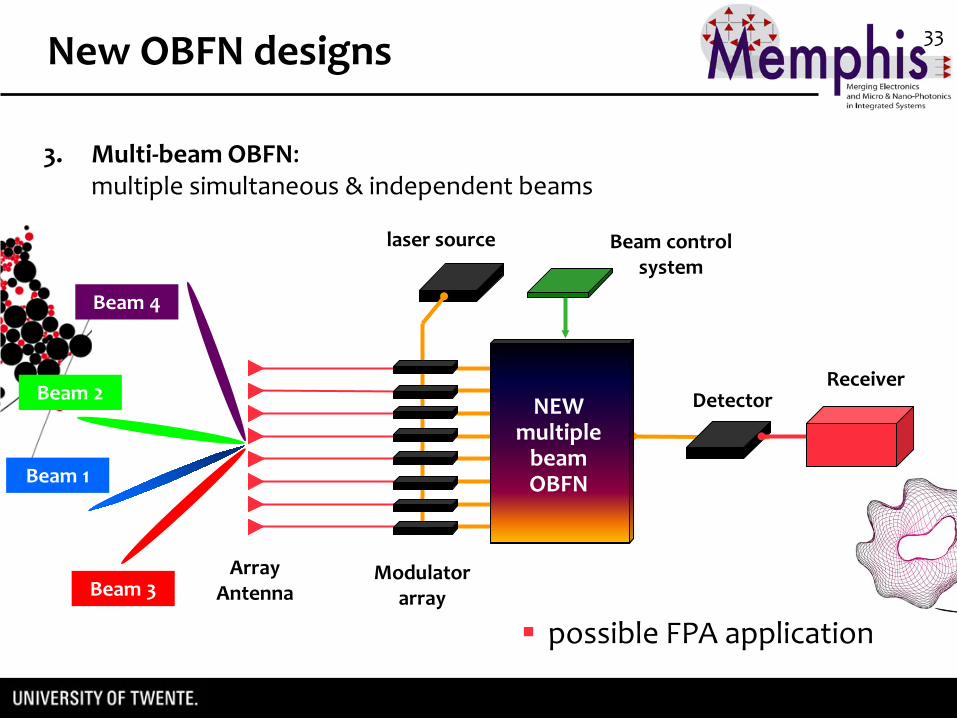
Optical beam forming network (OBFN): binary tree architecture Reduction in the number of rings
Ripple due to the Fabry-Perot reflections in the fiber connectors
ideal casemeasurement
[1] “RF-to-RF Characterization of a Phased Array Receive Antenna Steering System Using a Novel Ring Resonator-Based Integrated Photonic Beamformer”, L. Zhuang, M. Burla, C. G. H. Roeloffzen, A. Meijerink, D. A. I. Marpaung, M. R. H. Khan, W. van Etten, A. Leinse, M. Hoekman, R. G. Heideman, MWP 2009, Valencia, Spain, 14-16 Oct. 2009.
RF-to-RF characterization
16
OBFNfilter
RF output
RF input
4×1 splitter
mod.
mod.
mod.
mod.
delays tuned to compensate for different cable lengths
RF inputs terminated on matched loads: first in couples,
then individually
Matched loads
Power response (coherent combining)
RF-to-RF characterization
17
RF power output vs frequency
6 dB increase of the RF power level each time the number of combined signals is doubled
Coherent combining demonstrated
Power response (coherent combining) Results
~ 6 dB
~ 6 dB
RF-to-RF characterization
18
OBFN measurement: “SKY” demonstrator
Within SKADS (Square Kilometer Array Design Study)
19SKY demonstrator: an RF Photonic test bench
• Work carried on in ASTRON: modification of the EMBRACE phased array by using a photonic beamformer
• Operating band: 500-1500 MHz
• Use of a subarray of the original EMBRACE tile
Input 12
Input 11
Input 09
Input 10
4x1 array antenna
20
LNAs
Laser
OBFN chip
Detector
Modulators
4×1 subarray of Vivaldi antennas
near-field scanning
probe
OBFN controller
• Setup Sweeping laser
OSA
20 dBopticalsplitter
monitor opticaloutput
Modulator bias
SKY demonstrator
EMBRACE front-end
VNA
21
• Near-field antenna measurement
• Far-field are calculated using FFT on the basis of a near-field measurement
• IDEA: reduce the beamwidth θ by creating grating lobes
• Started by measuring an array of 2 AEs
• Because of the low frequency of the array compared to the room dimensions, difficult to measure large scan angles
Preliminary demonstrator
22
• Simulated patterns
-60 -40 -20 0 20 40 60-50
-45
-40
-35
-30
-25
-20
-15
-10
-5
0
Elevation [deg]
dire
ctiv
ity [d
Bi]
2×1, d = 3λ/215.9 deg
2×1, d = λ/255.6 deg
Preliminary demonstrator
23
~ Broadside
Preliminary demonstrator
24
- 14 deg
Preliminary demonstrator
25
• Antenna patterns: simulated vs measured
The radiation patterns measured for a 2 AEs array show a squint-freebeamsteering with at least 450 MHz instantaneous BW
(limited by the antenna test range only)
Preliminary demonstrator
26Towards optical integration
• Current work: extension to more antenna elements
• Difficulties: optical phase de-synchronization issues due to the presence of several meters of fiber between the splitting and the combining points generate output power fluctuations
• Need for integration to fully exploit the advantages given by the optical beamformer
• Current ongoing national and European projects (MEMPHIS, SANDRA) aim to a fully integrated system


![ROBUST ADAPTIVE BEAMFORMER WITH · PDF filebust adaptive beamforming, ... strained adaptive beamformer is studied in [5, 6] and widely used thereafter. Recently some interesting robust](https://static.documents.pub/doc/80x56/5ab383fc7f8b9ad9788e2684/robust-adaptive-beamformer-with-adaptive-beamforming-strained-adaptive.jpg)


