Page 1
Boston U
Larry A. Coldren
ECE & Materials, UC-Santa Barbara
Photonic-Integrated-Circuits
for Coherent Communication and Sensing
Major contributions by:
Mike Larson—Lumentum
Chris Doerr—Acacia
Beck Mason—Oclaro
Fred Kish—Infinera
UCSB Collaborators
Page 2
MOC 2018
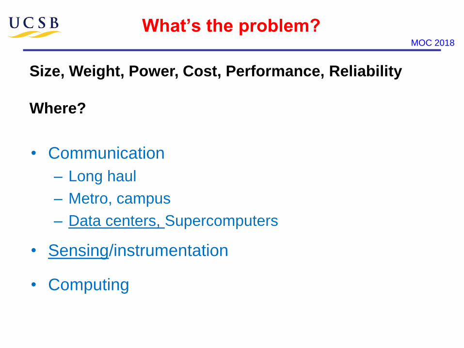
What’s the problem?
• Communication
– Long haul
– Metro, campus
– Data centers, Supercomputers
• Sensing/instrumentation
• Computing
Size, Weight, Power, Cost, Performance, Reliability
Where?
Page 3
MOC 2018
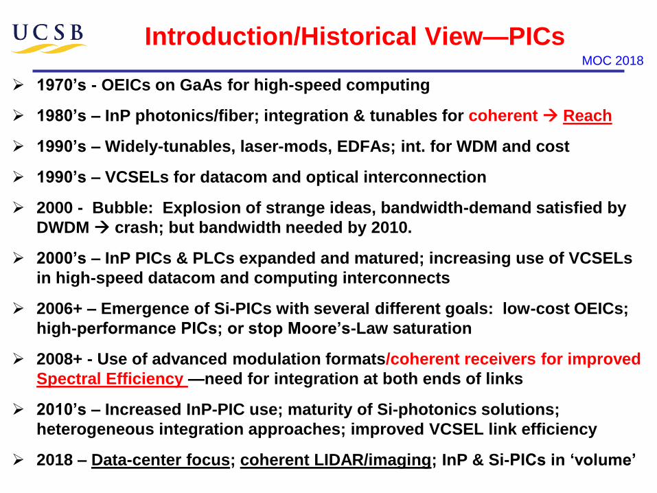
Introduction/Historical View—PICs
1970’s - OEICs on GaAs for high-speed computing
1980’s – InP photonics/fiber; integration & tunables for coherent Reach
1990’s – Widely-tunables, laser-mods, EDFAs; int. for WDM and cost
1990’s – VCSELs for datacom and optical interconnection
2000 - Bubble: Explosion of strange ideas, bandwidth-demand satisfied by
DWDM crash; but bandwidth needed by 2010.
2000’s – InP PICs & PLCs expanded and matured; increasing use of VCSELs
in high-speed datacom and computing interconnects
2006+ – Emergence of Si-PICs with several different goals: low-cost OEICs;
high-performance PICs; or stop Moore’s-Law saturation
2008+ - Use of advanced modulation formats/coherent receivers for improved
Spectral Efficiency —need for integration at both ends of links
2010’s – Increased InP-PIC use; maturity of Si-photonics solutions;
heterogeneous integration approaches; improved VCSEL link efficiency
2018 – Data-center focus; coherent LIDAR/imaging; InP & Si-PICs in ‘volume’
Page 4
INTREPIDIntelligent Reduction of Energy through Photonic Integration for Datacenters
‣ Photonics Integrated into Switch Packages– Points of highest bandwidth concentration
‣ Analog Coherent Links Optimized for Datacenters– Large sensitivity gain more energy efficient interconnects
– Enabling technology for WDM, photonic routing and switching
‣ Low-Power VCSEL Links– Ultra-low power connections from servers to ToR or EoR switches
‣ New Network Architectures– Exploring wavelength routing and switching
‣ Transition to Widespread Commercial Availability– Technology demo in live datacenter
– Open Compute Project (OCP), Telecom Infra Project (TIP)
Facebook OCP
“Backpack” switchFacebook OCP Rack
“Wedge” ToR switch
(ToR = Top of Rack)
InPlaserarrayFirstlevelchippackage
SwitchASIC
Typical datacenter
Fat Tree network
4
Page 6
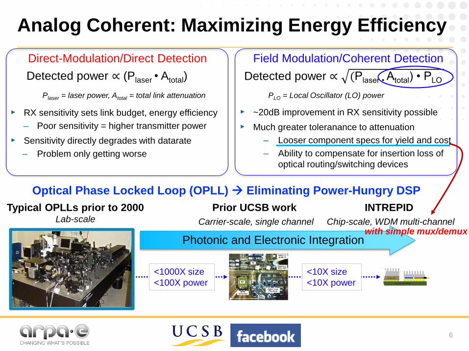
Analog Coherent: Maximizing Energy Efficiency
‣ RX sensitivity sets link budget, energy efficiency
– Poor sensitivity = higher transmitter power
‣ Sensitivity directly degrades with datarate
– Problem only getting worse
6
Direct-Modulation/Direct Detection Field Modulation/Coherent Detection
‣ ~20dB improvement in RX sensitivity possible
‣ Much greater toleranance to attenuation
– Looser component specs for yield and cost
– Ability to compensate for insertion loss of
optical routing/switching devices
Optical Phase Locked Loop (OPLL) Eliminating Power-Hungry DSP
Typical OPLLs prior to 2000Lab-scale
Prior UCSB work
Carrier-scale, single channel
Photonic and Electronic Integration
INTREPID
Chip-scale, WDM multi-channel
InPlaserarrayFirstlevelchippackage
SwitchASIC
<1000X size
<100X power
<10X size
<10X power
Detected power ∝ (Plaser • Atotal) Detected power ∝ (Plaser • Atotal) • PLO
Plaser = laser power, Atotal = total link attenuation PLO = Local Oscillator (LO) power
with simple mux/demux
Page 7
MOC 2018
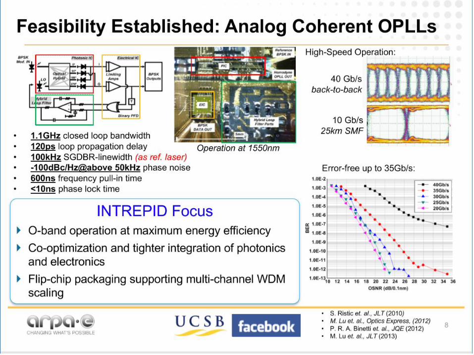
Prior Work: Phase Locked Coherent BPSK Receiver
“Analog Coherent”
OPLL + Costas Loop 1 cm2 footprint
Photonic IC: SGDBR laser, optical hybrid, and un-balanced PDs
Electronic IC: limiting amplifiers and phase & frequency detector (PFD)
Hybrid loop filter: Feed-forward technique, op-amplifier and 0603 SMDs
Fabricated by Mingzhi
Designed by Eli using
Teledyne 500nm HBT ProcessLoop filter and system
designed by Hyunchul
Mingzhi Lu, et. al., Optics Express, Vol. 20, Issue 9, pp. 9736-9741 (2012)
Page 8
MOC 2018
InP Widely-tunable Coherent Receiver PIC-2(Heterodyne or Intradyne—also for Optical Synthesis)
SGDBR laser 90 degree hybrid Four UTC photodetectorsSignal input
0.54mm
4.3 mm
• SG-DBR laser (LO)
• 30 mW output power
(~100 mW after SOA)
• 40 nm tuning range
• 25 mA threshold current
• 90 deg hybrid
• 1x2 MMI couplers
• Directional couplers
• Phase shifters
• UTC photodetectors
• 29 GHz 3-dB bandwidth with -2V
bias
• 18 mA saturation current at -5V
bias.
0 50 100 1500
10
20
30
Ou
tpu
t p
ow
er
/ m
W
Current / mA
0 50 100 1500
1
2
3
Vo
lta
ge
/ V
No phase error
4% power imbalance
0 1 2 3 4
x 1010
-20
-15
-10
-5
0
5
Frequency / Hz
Rela
tive R
F r
esponse / d
B
Mingzhi Lu, et. al., Optics Express, Vol. 20, Issue 9, pp. 9736-9741 (2012)
• I and Q outputs normally connected to ADC and DSP for Receiver
• Much lower SWaP-C Optical Phase Locked Loop (OPLL) used
SOA
Page 11
MOC 2018
From Chris Doerr--Acacia
For coherent use Vector modulation:
Page 12
© 2016 Lumentum Operations LLC | LUMENTUM CONFIDENTIAL AND PROPRIETARY INFORMATION 12ECOC 2018 Paper Mo3I.5
Waveguides: InP vs SiP (Lumentum Slides—M. Larson)
Waveguides in both systems are polarization sensitive
InP
p-InP
ridge
InGaAsP
(Q1.3)
n-InP
Dielectric
InP Shallow Ridge Waveguide
InP substrate
InP
p-InP
InGaAsP
Deep Ridge Waveguide
InP substrate
Si substrate
Si nanowire waveguide
Ridge width ~2um
Core thickness 200-300nm
Moderate index step
(3.4 <-> 3.17)
∆n ~ 0.2
Ridge width ~1.2-1.8um
Core thickness 200-300nm
Moderate vertical index
step
Large lateral index step
(3.3 <-> 1.45)
∆n ~ 2
450 x 220nm typical
Large index step vertical &
lateral (3.5 <-> 1.45)
∆n ~ 2
Si substrate
channel rib
n-InP
SiO2
Si
Page 13
© 2016 Lumentum Operations LLC | LUMENTUM CONFIDENTIAL AND PROPRIETARY INFORMATION 13ECOC 2018 Paper Mo3I.5
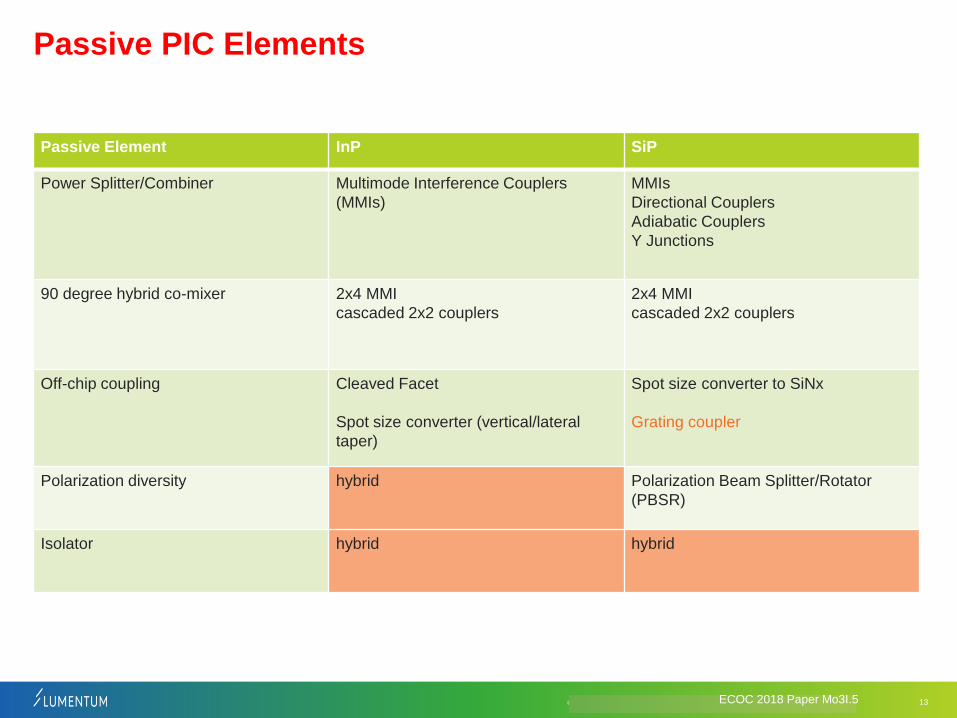
Passive PIC Elements
Passive Element InP SiP
Power Splitter/Combiner Multimode Interference Couplers
(MMIs)
MMIs
Directional Couplers
Adiabatic Couplers
Y Junctions
90 degree hybrid co-mixer 2x4 MMI
cascaded 2x2 couplers
2x4 MMI
cascaded 2x2 couplers
Off-chip coupling Cleaved Facet
Spot size converter (vertical/lateral
taper)
Spot size converter to SiNx
Grating coupler
Polarization diversity hybrid Polarization Beam Splitter/Rotator
(PBSR)
Isolator hybrid hybrid
Page 14
© 2016 Lumentum Operations LLC | LUMENTUM CONFIDENTIAL AND PROPRIETARY INFORMATION 14ECOC 2018 Paper Mo3I.5
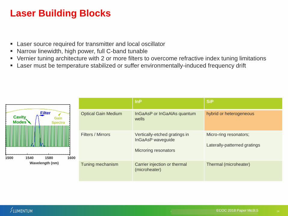
Laser Building Blocks
Laser source required for transmitter and local oscillator
Narrow linewidth, high power, full C-band tunable
Vernier tuning architecture with 2 or more filters to overcome refractive index tuning limitations
Laser must be temperature stabilized or suffer environmentally-induced frequency drift
InP SiP
Optical Gain Medium InGaAsP or InGaAlAs quantum
wells
hybrid or heterogeneous
Filters / Mirrors Vertically-etched gratings in
InGaAsP waveguide
Microring resonators
Micro-ring resonators;
Laterally-patterned gratings
Tuning mechanism Carrier injection or thermal
(microheater)
Thermal (microheater)
1500 1540 1580 1600
FilterCavity
ModesGain
Spectra
Wavelength (nm)
Page 15
© 2016 Lumentum Operations LLC | LUMENTUM CONFIDENTIAL AND PROPRIETARY INFORMATION 15ECOC 2018 Paper Mo3I.5
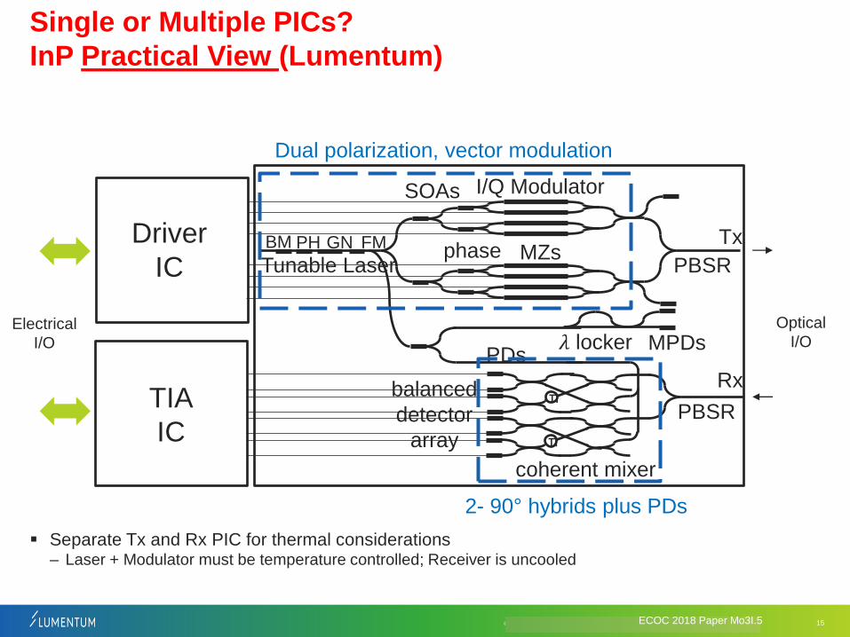
MZsphase
SOAs
MPDs
PBSR
PBSRπ
π
PDs
Tunable LaserGN FMBM PH Tx
RxTIA
IC
Driver
IC
coherent mixer
I/Q Modulator
Single or Multiple PICs?
InP Practical View (Lumentum)
Separate Tx and Rx PIC for thermal considerations– Laser + Modulator must be temperature controlled; Receiver is uncooled
Electrical
I/O
Optical
I/O
balanced
detector
array
𝜆 locker
Dual polarization, vector modulation
2- 90° hybrids plus PDs
Page 16
© 2016 Lumentum Operations LLC | LUMENTUM CONFIDENTIAL AND PROPRIETARY INFORMATION 16ECOC 2018 Paper Mo3I.5
Narrow linewidth thermally tuned Sampled Grating DBR
laser in InP (Lumentum)
Vernier-tuned SGDBR Laser, comb spacing ~700GHz
+16dBm output power, 100kHz linewidth
<1.4W Pdiss at 75C (laser TEC at 52C)
Front
MirrorGain Phase Back
MirrorSOA
microheaters
InGaAsP
MQW active
regions
Q1.3 tuning
waveguide
Sampled
gratingsThermal
isolation
Light
output
InP
substrate
0
0.02
0.04
0.06
0.08
0.1
0.12
191000 192000 193000 194000 195000 196000
Lin
ew
idth
(M
Hz)
Optical Frequency (GHz)
LineWidth
0
0.5
1
1.5
191000 192000 193000 194000 195000 196000
Pow
er
Dis
sip
ation (
W)
Optical Frequency (GHz)
Total Power dissipation at 75C (Laser+TEC)
16.1
16.2
16.3
16.4
16.5
191000 193000 195000Fib
er
Couple
d P
ow
er
(dB
m)
Optical Frequency (GHz)
Fiber Coupled Power
See Larson et al., OFC 2015, M2D.1
Page 17
© 2016 Lumentum Operations LLC | LUMENTUM CONFIDENTIAL AND PROPRIETARY INFORMATION 17ECOC 2018 Paper Mo3I.5
InP Coherent Tx PIC
Integrated Narrow Linewidth Tunable Laser
with Dual Polarization IQ modulator and
LO Output
Phase vs Bias Amplitude2 vs Bias
“Box” Sweeps Differential sweep
Bias=-4V
Maintain I and Q at
quadrature
Provide null-bias for
each child Mach-
Zehnder
Carry RF data
traffic
3.2 x 8 mm2
Page 18
© 2016 Lumentum Operations LLC | LUMENTUM CONFIDENTIAL AND PROPRIETARY INFORMATION 18ECOC 2018 Paper Mo3I.5
MZsphase
SOAs
MPDs
PBSR
PBSRπ
π
PDs
Tunable LaserGN FMBM PH Tx
RxTIA
IC
Driver
IC
coherent mixer
I/Q Modulator
Single or Multiple PICs?
SiP Preferred View (Acacia, NTT)
Separate Tunable Laser PIC from Modulator+Receiver PIC for thermal considerations
Electrical
I/O
Optical
I/O
balanced
detector
array
𝜆 locker
K. Kikuchi et al., Compound Semiconductor Integrated Circuit Symposium (CSICS), 2017C. Doerr et al., OFC 2016
Page 21
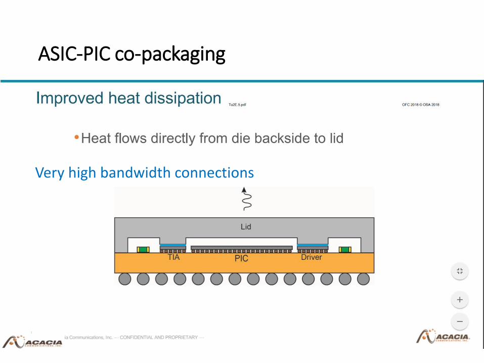
ASIC-PIC co-packaging
Very high bandwidth connections
Page 22
© 2016 Lumentum Operations LLC | LUMENTUM CONFIDENTIAL AND PROPRIETARY INFORMATION 22ECOC 2018 Paper Mo3I.5
Modulator Material Physics
InP: Quantum Confined Stark Effect
– Applied reverse bias causes a redshift of the
multiple quantum well excitonic absorption edge
– ∆𝑛 ∝ 𝑉,𝑉2
n n++pp++
wd
‘Soref’ equation. Fitting parameters are empirical
Soref and Bennett. IEEE JQE 23.1 (1987): 123-129.
p-InP
InP substrate
n-InP
InGaAsP
or
InGaAlAs
MQW
D.A.B Miller, et al., Phys. Rev. Lett., 53 (1984) p. 2174
1.25 1.3 1.35 1.4 1.45 1.5 1.55 1.6
x 10-6
0
1000
2000
3000
4000
5000
6000
7000
8000
9000
10000
Wavelength (nm)
Sig
nal
More
negative
bias
SiP: plasma dispersion effect
– ∆𝑛 ∝ carrier concentration ∆𝑁, ∆𝑃.
– Carrier concentration is a non-linear function of applied
V
Si
Page 23
© 2016 Lumentum Operations LLC | LUMENTUM CONFIDENTIAL AND PROPRIETARY INFORMATION 23ECOC 2018 Paper Mo3I.5
LiNbO3 (ideal) InP: Lumentum measurements SiP: McGill measurements
V (static)
rad or dB
(5mm devices)
Attenuation [dB]
Phase [rad]
∅ ∝ 𝑽 ∅ ∝ 𝑽, 𝑽𝟐 ∅ ∝…complicated
Lumentum/McGill NSERC Project, SiP MZM design work, Fall 2016 (M Jacques, A Samani, J Sonkoly)
Phase Shifter Transfer Functions
Phase & attenuation vs applied voltage for 3 modulator materials
– InP: nonlinear phase and attenuation (electro-absorption) with increasing reverse bias
– SiP: complicated phase and attenuation; notice: vertical scale range is ½, horizontal scale (V) is 2.5X
Page 24
© 2016 Lumentum Operations LLC | LUMENTUM CONFIDENTIAL AND PROPRIETARY INFORMATION 24ECOC 2018 Paper Mo3I.5
Power Dissipation Budget Comparison:
64 Gbaud DP-16QAM IC-TROSA component level estimate
Conservative estimates for budgetary purpose
InP PIC + TEC is 3.3W vs. 2.3W for SiP + External Laser: 1W SiP advantage
SiP solution is disadvantaged by high Vpp => high driver power dissipation
Power dissipation
Item (max)
InP
IC-TROSA
Tx PIC + Rx PIC
SiP
IC-TROSA
TxRx PIC + Laser PIC
Notes
Tx PIC active load (W) 0.9 0.1 InP case includes laser
Tx TEC (W) 2.4 0
External Laser + TEC
(W)0 2.2 SiP case only
Driver (W) 1.9 3.5
TIA (W) 1.1 1.1
Total (W) 6.3 6.9 maximum
Page 25
© 2016 Lumentum Operations LLC | LUMENTUM CONFIDENTIAL AND PROPRIETARY INFORMATION 25ECOC 2018 Paper Mo3I.5
Summary
As long as laser is temperature sensitive and requires TEC, single PIC
solution is unlikely the lowest power dissipation– At 1310 may be able to use uncooled laser
High Vpi of SiP modulator is a challenge for driver power dissipation
and scaling to higher baud rates– SiP modulators may not be good choices within data centers
Page 26
26© 2018 Oclaro, Inc. │ Confidential and Proprietary
InP Modulator Integration Evolution
64 Gbaudfold MZ-SOA
43 Gbaudfold MZ-SOA
64 GbaudMZ-SOA
2008 2013 2014 2015 2016 2017 2018 2019 202032 GbaudMZ-SOA
100/200G Coherent Transmission
100/200G ULH and 600G Metro/Edge
200G Low power compact
400G CDM
SOAintegration
Multi-MZ PIC
High bandwidth Design
SI wafer process
Folded architecture
100 Gbaudfold MZ-SOA
1T single l
High-temp Low-dissipation
400G Low Power
100Gbaud wafer process
Accelerating InP modulator PIC development
• Increasing integration and functionality
• Higher modulation rates• Low cost optics architecture• Efficiency improvements
20 GbaudQPSK MZ
AlQmaterials
Page 27
27© 2018 Oclaro, Inc. │ Confidential and Proprietary
InP Receiver PIC Integration Evolution2011 2013 2014 2015 2016 2017 2018 2019 202020Gbaud QPSK Rx
Accelerating InP modulator PIC development
• Increasing integration and functionality
• Higher modulation rates• Low cost optics architecture
32Gbaud Rx
Miniaturisation
100/200G Coherent Receiver
100-600G Coherent Receiver
100-400G CompactIntegration
Integrated VOA
64 Gbaud Dual-Rx
100Gbaud wafer process
1T single l
100 Gbaud Rx
Page 28
28© 2018 Oclaro, Inc. │ Confidential and Proprietary
64 Gbaud Tx & Rx dual channel 400G today
Integrated CompactRx/VOA
Folded MZ-SOA Tx
Page 29
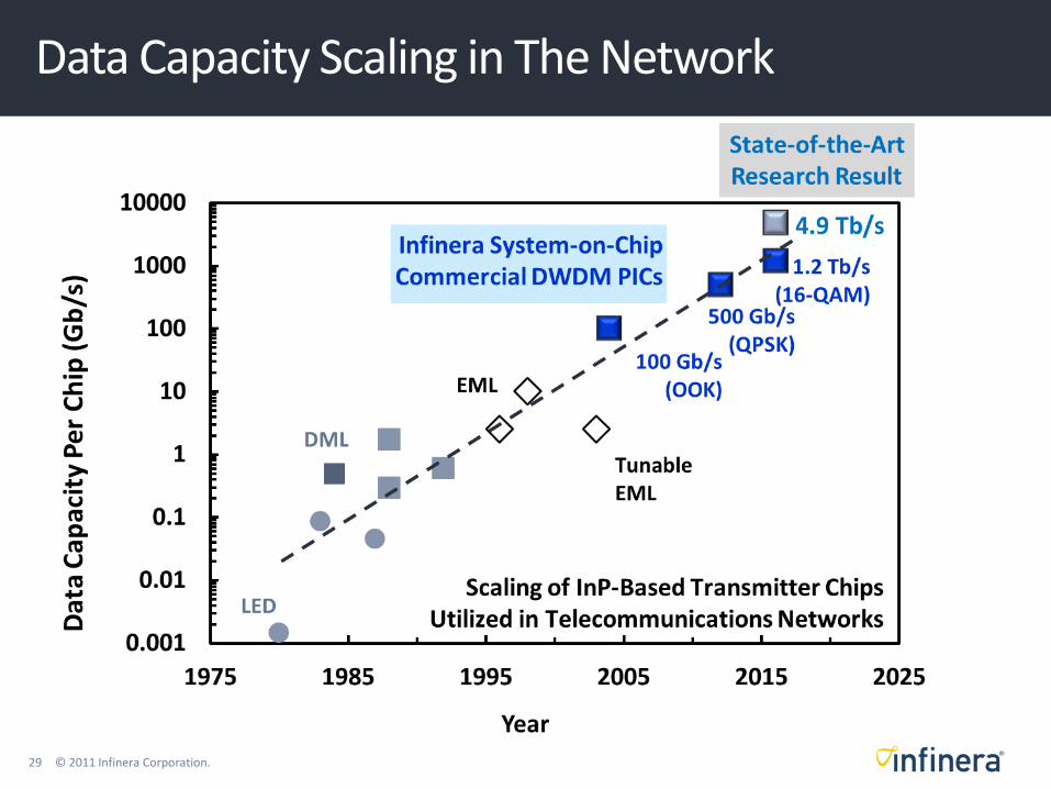
29 © 2011 Infinera Corporation.
Data Capacity Scaling in The Network
Page 30
30 © 2011 Infinera Corporation
Photonic Module Evolution
F. Kish, et al, JSTQE, 24 (1) 2018
Page 31
31 © 2011 Infinera Corporation
2011: 500 Gb/s PM-QPSK Coherent PICs
Tx PIC Architecture (5 x 114 Gb/s)
• > 450 Integrated Functions• 8 Different Integrated Functions
Rx PIC Architecture (5x 114Gb/s)
• > 150 Integrated Functions• 7 Different Integrated Functions
Page 32
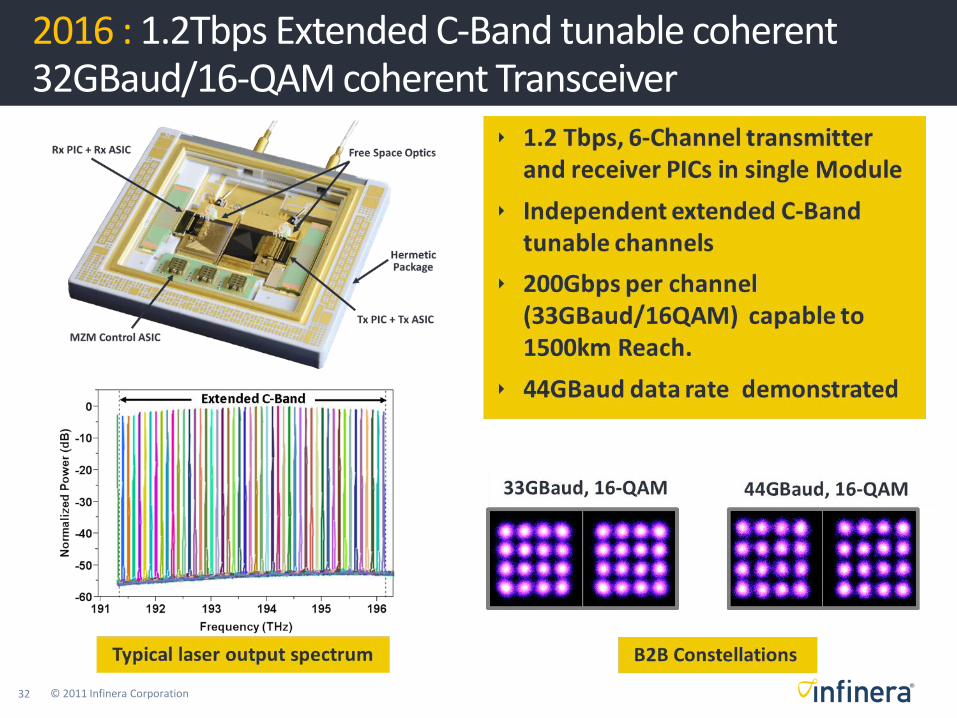
32 © 2011 Infinera Corporation
2016 : 1.2Tbps Extended C-Band tunable coherent 32GBaud/16-QAM coherent Transceiver
Page 33
33 © 2011 Infinera Corporation
Back-to-back transmitter constellations on PIC with potential capacity of 4.9 Tb/s
F. Kish, et al, JSTQE, 24 (1) 2018
Page 34
MOC 20182D-Beam Sweeping
• Our approach: 1D array + grating
• Scaling as N + 1, not N2
1xN
Grating Emitter ArrayPhase Ctrl(lateral-steering)
Widely-tunable laser(longitudinal-steering)
lateral
longitudinal
• Lateral beam-steering via phase-shifter array, ψ
• Longitudinal beam-steering via wavelength-tuned grating diffraction, θ
W. Guo, et al, OFC ‘13, Mar. 21, 2013
1 (wavelength)
N (number of waveguides)
DARPA-SWEEPER
Page 35
MOC 2018
PMs(32)
SOAs(32)
EAPDs(32)
M1 M2GT
Tunable Laser Splitter
EmittingArrayShuttering pre-amplifier
On-Chip Monitor
P-A
32 x N: Surface-emitting grating phased-array
Optical Beam SWEEPER—InP-PIC
• Waveguide spacing varied to suppress lateral side lobes.
• Grating duty-factor weighted to extend effective length
• Nearly Gaussian shape
3.5
mm
9.6 mm
Tunable laser Splitter SOAPhaseshifter Grating Monior
Surface ridge Surface ridgeDeep ridge Deep ridge Surface ridge
Integrated SGDBR tuning
Powers into 32 SOAs
y
x
Page 36
MOC 2018
• 2D beam steering demonstrated
(1545nm, 0)
(1524nm, 5)
(1524nm, -5)(1567nm, -5)
(1567nm, 5)
2D Beam Sweeping results (32 x N)
Far-field beam profiles (x & y)
1.2 x 0.3°
N ~ 120
-20 dB sidelobes
Flip-chipped PIC-on-carrier110 good contacts
W. Guo, et al, OFC ‘13, Mar., 2013
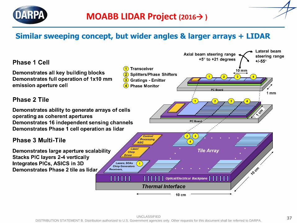
Page 37
UNCLASSIFIED
DISTRIBUTION STATEMENT B. Distribution authorized to U.S. Government agencies only. Other requests for this document shall be referred to DARPA.37
MOABB LIDAR Project (2016 )
Similar sweeping concept, but wider angles & larger arrays + LIDAR
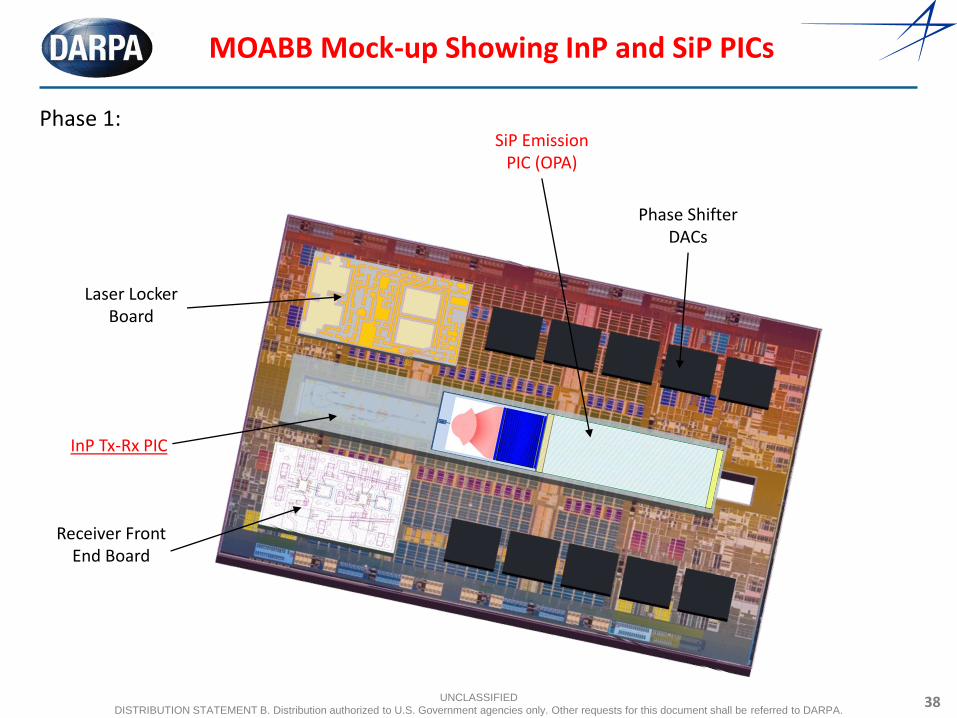
Page 38
UNCLASSIFIED
DISTRIBUTION STATEMENT B. Distribution authorized to U.S. Government agencies only. Other requests for this document shall be referred to DARPA.38
MOABB Mock-up Showing InP and SiP PICs
SiP Emission PIC (OPA)
Phase Shifter DACs
Laser Locker Board
Receiver Front End Board
InP Tx-Rx PIC
Phase 1:
Page 39
UNCLASSIFIED
DISTRIBUTION STATEMENT B. Distribution authorized to U.S. Government agencies only. Other requests for this document shall be referred to DARPA.39
Schematic of InP Transceiver PIC
Locker Electronics
output
Receiver Electronics
SiP
LO
return
SOAs
FMCW LIDAR Transceiver
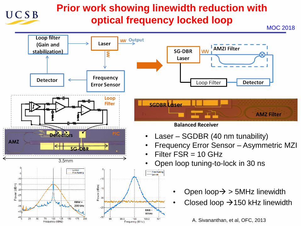
Page 40
MOC 2018
Prior work showing linewidth reduction with
optical frequency locked loop
SGDBR Laser
AMZ Filter
Balanced Receiver
• Laser – SGDBR (40 nm tunability)
• Frequency Error Sensor – Asymmetric MZI
• Filter FSR = 10 GHz
• Open loop tuning-to-lock in 30 ns
SG-DBR
AMZ
Detectors
3.5mm
Loop Filter
PIC
• Open loop > 5MHz linewidth
• Closed loop 150 kHz linewidth
A. Sivananthan, et al, OFC, 2013
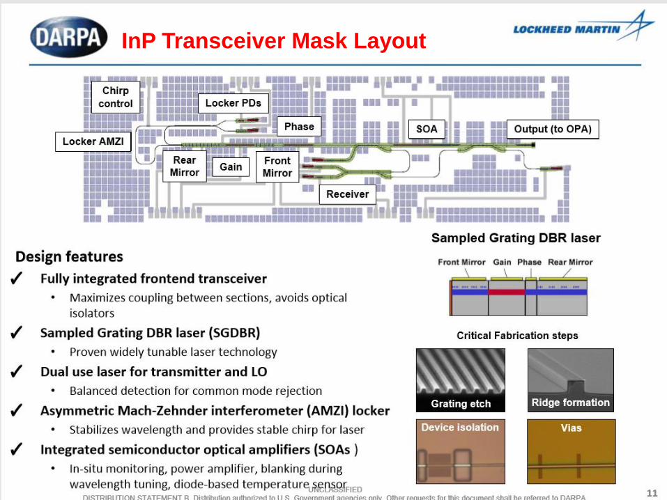
Page 41
MOC 2018
InP Transceiver Mask Layout
Page 42
MOC 2018
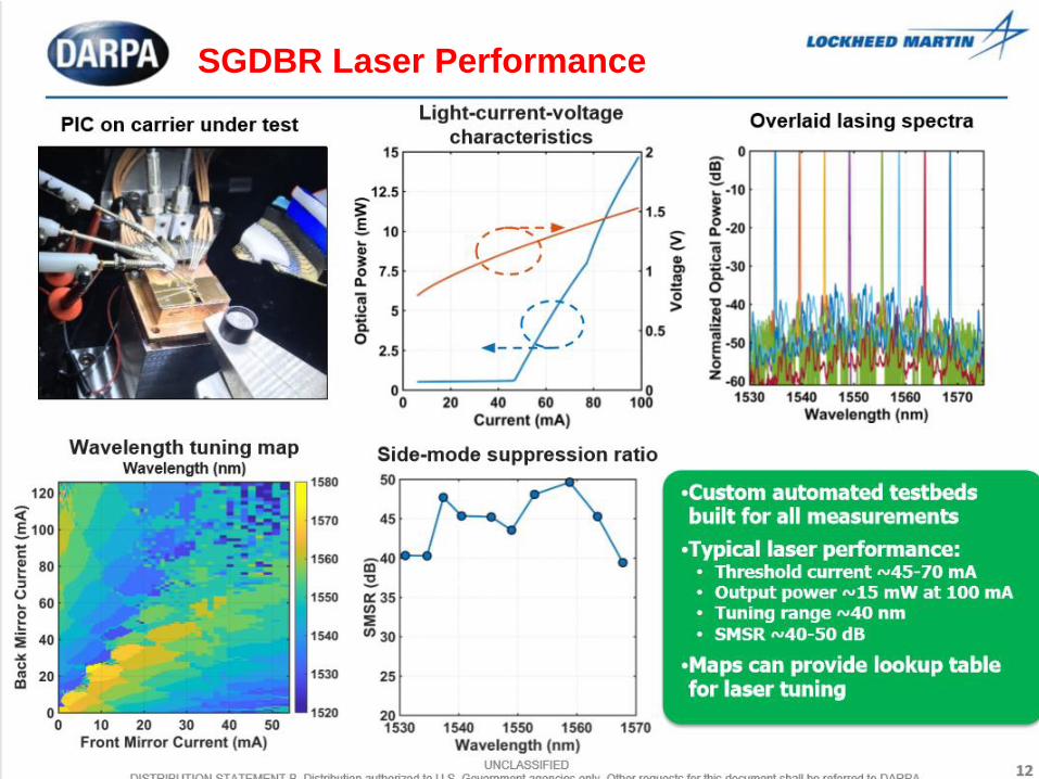
SGDBR Laser Performance
Page 43
MOC 2018
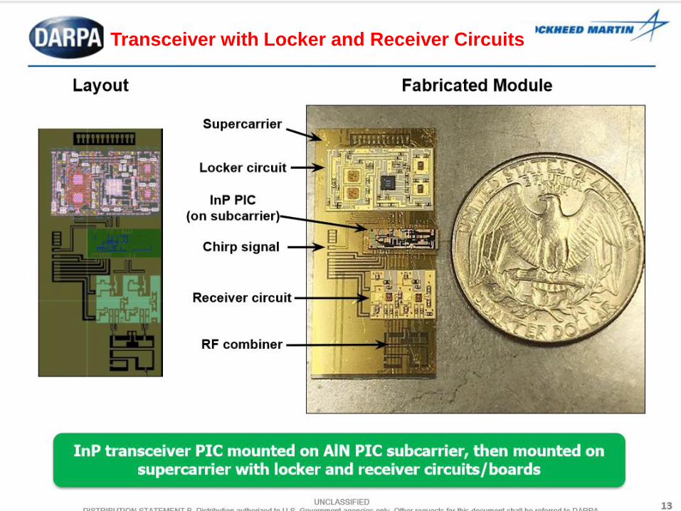
Transceiver with Locker and Receiver Circuits
Page 44
MOC 2018
Locker and Receiver PD outputs
AMZI frequencyLaser frequency(Mode spacing= 45 GHz)
Tune AMZI filter
Laser frequency
Tune Laser
30 GHz
PD-1, PD-2
Page 45
MOC 2018
Output coupling to SiP emitter PIC
Page 46
UNCLASSIFIED
DISTRIBUTION STATEMENT B. Distribution authorized to U.S. Government agencies only. Other requests for this document shall be referred to DARPA.46
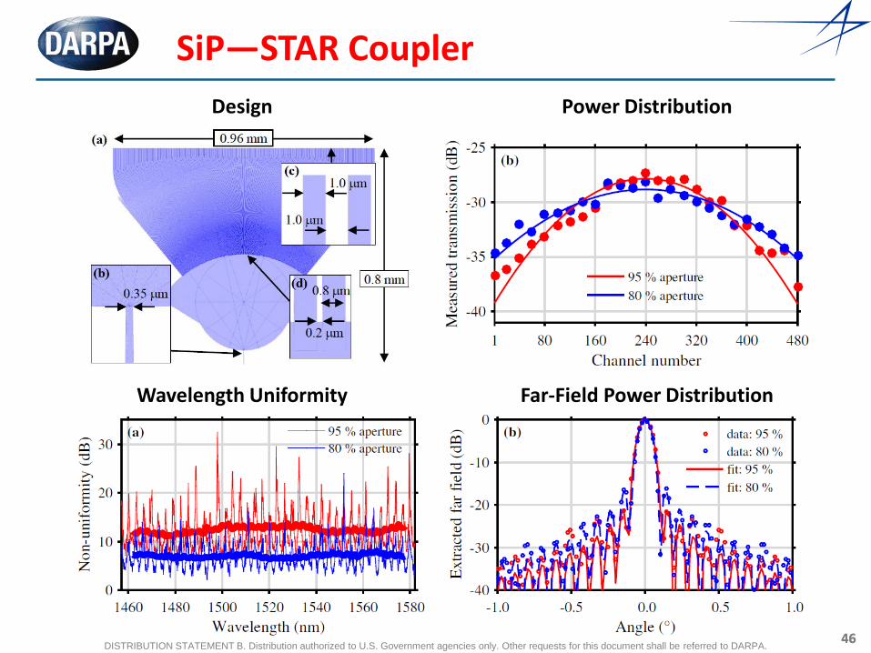
SiP—STAR Coupler
46
Design Power Distribution
Wavelength Uniformity Far-Field Power Distribution
Page 47
UNCLASSIFIED
DISTRIBUTION STATEMENT B. Distribution authorized to U.S. Government agencies only. Other requests for this document shall be referred to DARPA.47
SiP-OPA full-run PIC
1
2
3 4 5 6
22 mm
26
mm
Bonded epi
1. Deep etch: Directional couplers, ring resonators and loop mirrors test structures
2. Modulator test structures (MZI, loss spiral)
3. 32-channel devices (can be probed)
4. Reduced pitch 240-channel full device (to be bonded to interposer)
5. Standard pitch 240-channel full device (to be bonded to interposer)
6. Shallow etch: Directional couplers, ring resonators and loop mirrors test structures + loss spirals (both etch depths)
6 dies per 4 inch (100 mm) wafer
Page 48
MOC 2018
Take-Aways
• PICs are desirable for modest to high volume communication and sensing applications, where size, weight, power and cost (SWAP-C) reductions are desired.
• PICs are important because of the inherently stable phase relationships and possibly seamless interfaces between elements.
• PICs generally bring better reliability once properly designed; yield and some aspects of performance may be compromised, although other aspects can be improved.
• Although InP-PICs are currently being produced in higher volume, the use of SiP-PICs is growing more rapidly.