Photonic non-volatile memories using phase change materials Wolfram H. P. Pernice and Harish Bhaskaran Citation: Appl. Phys. Lett. 101, 171101 (2012); doi: 10.1063/1.4758996 View online: http://dx.doi.org/10.1063/1.4758996 View Table of Contents: http://apl.aip.org/resource/1/APPLAB/v101/i17 Published by the American Institute of Physics. Related Articles The influence of resistance drift on measurements of the activation energy of conduction for phase-change material in random access memory line cells J. Appl. Phys. 112, 084506 (2012) Electrical conduction in chalcogenide glasses of phase change memory App. Phys. Rev. 2012, 8 (2012) Electrical conduction in chalcogenide glasses of phase change memory J. Appl. Phys. 112, 071101 (2012) Understanding the multistate SET process in Ge-Sb-Te-based phase-change memory J. Appl. Phys. 112, 064901 (2012) Highly sensitive tactile sensors integrated with organic transistors Appl. Phys. Lett. 101, 103308 (2012) Additional information on Appl. Phys. Lett. Journal Homepage: http://apl.aip.org/ Journal Information: http://apl.aip.org/about/about_the_journal Top downloads: http://apl.aip.org/features/most_downloaded Information for Authors: http://apl.aip.org/authors
Transcript
Photonic non-volatile memories using phase change materialsWolfram H. P. Pernice and Harish Bhaskaran Citation: Appl. Phys. Lett. 101, 171101 (2012); doi: 10.1063/1.4758996 View online: http://dx.doi.org/10.1063/1.4758996 View Table of Contents: http://apl.aip.org/resource/1/APPLAB/v101/i17 Published by the American Institute of Physics. Related ArticlesThe influence of resistance drift on measurements of the activation energy of conduction for phase-changematerial in random access memory line cells J. Appl. Phys. 112, 084506 (2012) Electrical conduction in chalcogenide glasses of phase change memory App. Phys. Rev. 2012, 8 (2012) Electrical conduction in chalcogenide glasses of phase change memory J. Appl. Phys. 112, 071101 (2012) Understanding the multistate SET process in Ge-Sb-Te-based phase-change memory J. Appl. Phys. 112, 064901 (2012) Highly sensitive tactile sensors integrated with organic transistors Appl. Phys. Lett. 101, 103308 (2012) Additional information on Appl. Phys. Lett.Journal Homepage: http://apl.aip.org/ Journal Information: http://apl.aip.org/about/about_the_journal Top downloads: http://apl.aip.org/features/most_downloaded Information for Authors: http://apl.aip.org/authors
Photonic non-volatile memories using phase change materials
Wolfram H. P. Pernice1,a) and Harish Bhaskaran2
1Institute of Nanotechnology, Karlsruhe Institute of Technology, 76344 Eggenstein-Leopoldshafen, Germany2School of Engineering, University of Exeter, Exeter EX4 4QF, United Kingdom
(Received 2 July 2012; accepted 7 August 2012; published online 22 October 2012)
We propose an all-photonic, non-volatile memory, and processing element based on phase-change
thin-films deposited onto nanophotonic waveguides. Using photonic microring resonators partially
covered with Ge2Sb2Te5 (GST) multi-level memory operation in integrated photonic circuits can
be achieved. GST provides a dramatic change in refractive index upon transition from the
amorphous to crystalline state, which is exploited to reversibly control both the extinction ratio and
resonance wavelength of the microcavity with an additional gating port in analogy to optical
transistors. Our analysis shows excellent sensitivity to the degree of crystallization inside the GST,
thus providing the basis for non-von Neumann neuromorphic computing. VC 2012 American Instituteof Physics. [http://dx.doi.org/10.1063/1.4758996]
The ability to write, store, and retrieve data is at the very
heart of information processing. Various techniques are
employed to efficiently cope with the vast spread of speed
and long term storage needs. In particular, phase change
memories (PCMs) promise to revolutionize the field of infor-
mation processing by bridging the gap between the short-
term, but very quick operation of on-chip memories and the
long-term, but relatively slow storage systems such as solid-
state devices and hard-drives.1–3 Not only can phase change
materials switch in a matter of picoseconds,4–6 they are also
able to retain information for very long periods of time.2,7 In
addition, they scale extremely well to the nanoscale, with
present-day demonstrations of 6 nm cells employing electri-
cal switching.7,8 Specifically, Ge2Sb2Te5 (GST) is the most
commonly used alloy for such applications. By reversibly
transforming the crystalline structure between amorphous
and crystalline states using electrical pulses, the resistive
properties of the thin film can be varied by several orders of
magnitude.9 PCMs also demonstrate a large difference in
reflectivity upon phase-transition, an effect that has led to
their commercial use in optical storage discs, such as DVDs
and Blue-Ray discs.10
Herein, we propose a chalcogenide-based integrated pho-
tonic memory element, with the ability for sub-nanosecond
reading and writing, while still retaining data for several
years. We analyze the photonic architecture as illustrated in
Fig. 1(a), which comprises a microring resonator coupled to
nanophotonic waveguides. In contrast to photonic memories
and mechanical resonators,11 the photonic circuit allows for
static tunability which is maintained when the control light
has been switched off. We base our analysis on silicon
nitride-on-insulator substrates for broadband optical applica-
tions. Silicon nitride can be used to fabricate high-quality
nanophotonic components for both telecoms and visible
applications.12,13 The feeding waveguide is optimized for sin-
gle mode operation at 1550 nm input wavelength. Inside the
ring resonator, a small region of the waveguide is suspended
similar to waveguides used for nanomechanical sensing14 and
opto-mechanical operation.15 A thin film of phase change
material (GST) is deposited on this suspended region, and
forms the basis of the non-volatile memory element of this
device. The use of phase change materials, particularly
GST, is explored as these materials undergo reversible trans-
formations between crystalline and amorphous states upon
application of energy. We consider suspended waveguides to
improve thermal isolation of the switching region to ensure
FIG. 1. (a) Schematic overview of the proposed memory element. Light
from a control port (red) is coupled evanescently to the ring resonator to per-
form the switching operation of the GST through photothermal heating. (b)
A cross-sectional view of the coupling region showing the control port on
the left side and the GST covered free-standing waveguide section on the
right side. (c) The calculated modal profiles of the GST covered waveguide
cross-section when the GST is in the amorphous state (left panel) and the
that the GST reaches a temperature sufficient to lead to
heating-induced crystallization/amorphization with a short
thermal time constant. In order to control the temperature in
the suspended section optically, a second control port is
coupled evanescently to the GST section, where a separate
tuning light can be applied independently of the probe light
transmitted through the feeding waveguide as shown in Fig.
1(b). By varying the coupling gap between the control port
and the ring resonator, the degree of heat transfer into the
GST thin film can be geometrically defined.
Light travelling inside the ring resonator couples evan-
escently to the GST. By changing the crystallization of the
GST, both the refractive index of the GST and the material
absorption vary by a large margin. This significantly affects
the modal profile of the propagating mode as shown in the
calculated results in Fig. 1(c) using COMSOL MULTIPHYSICS.
The transition from the crystalline to the amorphous state
induces significant variation in the modal absorption of the
material which directly affects the performance of the optical
resonator. When the GST is in the amorphous state, the
modal profile resembles an optical mode confined largely
into the silicon nitride portion of the waveguide. Due to low
material absorption in this state, the optical mode is thus
largely guided inside the silicon nitride and hence propagates
without significant optical loss. Upon switching into the
crystalline state, the material becomes significantly more
absorptive and metal-like, leading to stronger coupling to the
GST thin film (see Fig. 1(c), right panel). As a result, the
mode is confined closer to the metal-like portion, which
leads to enhanced optical absorption thus increasing the
round-trip loss through the ring resonator.
We analyze the transmission properties of the ring
resonator device using coupled mode-theory16 (CMT) and
finite-difference time-domain (FDTD) simulations.17 Here, a
micro-ring resonator with a radius of 10 lm is considered,
which provides a small footprint nanophotonic circuit ele-
ment. The waveguide cross-section is set to 700� 330 nm2,
corresponding to our previously fabricated waveguide
design.18 The GST covered section is assumed to be 0.5 lm
long. Assuming typical propagation loss in the silicon nitride
waveguide of 3 dB/cm as measured previously,18 the chosen
parameters provide a compromise between optical Q and
free-spectral range (FSR). Indeed, in order to obtain wider
bandwidth operation, it is advantageous to operate the device
in a lower Q regime. We initially consider the performance
of the device in the amorphous material state. We employ
the refractive index profile shown in Fig. 2(a) to extract the
complex refractive index in dependence of wavelength. For
use with the FDTD method, the refractive index profile is
modeled as a multi-pole Lorentzian material over the wave-
length range of interest around 1550 nm.19 In Fig. 2(a), the
markers denote the data taken from,20 while the solid lines
represent the multi-Lorentzian fit in good agreement with the
measured values. Knowing the roundtrip loss adB in units of
dB/cm, the optical quality factor can then be estimated
as Q ¼ 10 log10e � 2png=kadB.21 From the CMT-model, the
transmission in the through port shows characteristic
resonances with a FSR of 48.2 nm as presented in Fig. 2(b)
for a critically coupled device. From the CMT-simulations,
we estimate an optical quality factor of 9400, equivalent to a
linewidth of 160 pm. As shown in Fig. 2(c), the CMT esti-
mations are also confirmed by the FDTD calculations, as
indicated by the overlaid markers in Fig. 2(c).
When tuning the probe wavelength transmitted through
the feeding waveguide onto resonance, the transmitted signal
in the output port is strongly attenuated. Upon switching into
the crystalline state, the round-trip loss inside the ring reso-
nator is strongly increased due to the enhanced material
absorption in the GST. As a result, both the coupling and res-
onance condition of the resonator are modified significantly.
Because the round-trip losses have increased, the existing
coupling gap leads to an undercoupled ring resonator, thus
increasing the transmission in the through port. This is illus-
trated in Fig. 3(a), where we show the dependence of the de-
vice performance on both wavelength and the degree of
crystallization. The degree of crystallization r is defined as
the volumetric proportion of crystalline material inside the
GST, where r ¼ 0 corresponds to an entirely amorphous
GST and r ¼ 1 to a fully crystalline structure. When the
round-trip loss is increased, not only the transmission in the
through port but also the width of the resonance increases.
For higher round-trip loss, stronger coupling into the ring
resonator would be required, corresponding to a small cou-
pling gap. Because the gap was optimized for critical cou-
pling for the device with lower roundtrip loss, the larger gap
leads thus to a weakly coupled device when the GST has
fully switched into the crystalline state. This is illustrated
further in the cross-sectional plots in Fig. 3(b), which are
taken at the intersection dashed line in Fig. 3(a). By switch-
ing between the amorphous and crystalline state, the trans-
mission past the resonator can be varied between 0% and
FIG. 2. (a) The refractive index of GST in dependence of wavelength used
during the CMT and FDTD modeling. Markers are taken from Ref. 20,
while the solid lines represent the multi-Lorentzian fit. The relevant wave-
lengths for the control light (orange) and the probe light (purple) are marked.
(b) The calculated transmission spectrum of a ring resonator critically
coupled in the amorphous state (blue curve). Upon switching the GST into
the crystalline state, the transmission profile changes significantly (red
curve). (c) Zoom into a resonance at 1546 nm, showing optical Q of 9400.
171101-2 W. H. P. Pernice and H. Bhaskaran Appl. Phys. Lett. 101, 171101 (2012)
90%, thus providing extinction ratio of more than 10 dB. By
controlling the degree of crystallization, we are able to con-
tinuously tune the transmission behavior of the device
between the low and high transmission operation. By assign-
ing memory levels to chosen threshold levels of the transmis-
sion curve, it is thus possible to discriminate between
multiple levels of GST crystallization.
We then compute the power of the laser light in the control
port required to melt the GST. When the memory cell is oper-
ated, the state is readout with a weak probe light placed on the
ring resonance, which does not disturb the state of the GST.
The control port on the other hand is employed to deliver high
intensity optical pulses, which transform the phase composi-
tion of the GST. The complex refractive index of the material
is related to the material absorption. We assume that the
absorbed light is converted completely to heat inside the wave-
guide. Because the material absorption of GST is much higher
in the visible wavelength range, we employ control light at
700 nm to perform the heating operation. From the intensity
profile, we are able to extract the thermal properties of the sys-
tem by solving the transient heat transfer equation as a result of
conduction, where the thermal material parameters for GST
are taken from Ref. 22. The structure is excited with an optical
pulse of 600 fs width. From the numerical analysis, we find
that at writing power of less than 5.4 pJ, we can raise the tem-
perature inside the released waveguide section to 400� and
therefore transform the GST into a crystalline state.
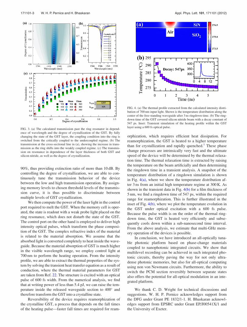
Reversibility of the device requires reamorphization of
the crystalline GST, a process that depends on the fall times
of the heating pulse—faster fall times are required for ream-
orphization, which requires efficient heat dissipation. For
reamorphization, the GST is heated to a higher temperature
than for crystallization and rapidly quenched.1 These phase
change processes are intrinsically very fast and the ultimate
speed of the device will be determined by the thermal relaxa-
tion time. The thermal relaxation time is extracted by raising
the temperature on the beam artificially and then determining
the ringdown time in a transient analysis. A snapshot of the
temperature distribution of a ringdown simulation is shown
in Fig. 4(a), where we show the temperature distribution af-
ter 3 ns from an initial high temperature regime at 300 K. As
shown in the transient data in Fig. 4(b) for a film thickness of
5 nm, we find a ringdown time of 547 ps, within the required
range for reamorphization. This is further illustrated in the
inset of Fig. 4(b), where we plot the temperature evolution in
the GST under optical excitation with a 600 fs pulse.
Because the pulse width is on the order of the thermal ring-
down time, the GST is heated very efficiently and subse-
quently cools down within a sub-nanosecond time interval.
From the above analysis, we estimate that multi-GHz mem-
ory operation of the devices is possible.
In conclusion, we have introduced an all-optically tuna-
ble photonic platform based on phase-change materials
coupled to nanophotonic integrated circuits. We show that
multilevel recording can be achieved in such integrated pho-
tonic circuits, thereby paving the way for not only ultra-
dense photonic memories, but also for all-optical computing
using non von Newmann circuits. Furthermore, the ability to
switch the PCM section reversibly between separate states
also offers the potential for all-optical modulation in an inte-
grated platform.
We thank C. D. Wright for technical discussions and
suggestions. W. H. P. Pernice acknowledges support from
the DFG under Grant PE 1832/1-1. H. Bhaskaran acknowl-
edges support from EPSRC under Grant EP/J00541X/1 and
the University of Exeter.
FIG. 3. (a) The calculated transmission past the ring resonator in depend-
ence of wavelength and the degree of crystallization of the GST. By fully
changing the state of the GST layer, the coupling condition into the ring is
switched from the critically coupled to the undercoupled regime. (b) The
transmission at the cross-sectional line in (a), showing the increase in trans-
mission as the ring shifts into the weakly coupled regime. (c) The transmis-
sion on resonance in dependence of the layer thickness of both GST and
silicon nitride, as well as the degree of crystallization.
FIG. 4. (a) The thermal profile extracted from the calculated intensity distri-
bution of 700 nm input light. Shown is the temperature distribution along the
center of the free-standing waveguide after 3 ns ringdown time. (b) The ring-
down time of the GST covered silicon nitride beam with a decay constant of
547 ps. Inset: Transient simulation of the heating profile within the GST
layer using a 600 fs optical pulse.
171101-3 W. H. P. Pernice and H. Bhaskaran Appl. Phys. Lett. 101, 171101 (2012)
1S. Raoux, G. W. Burr, M. J. Breitwisch, C. T. Rettner, Y. C. Chen, R. M.
Shelby, M. Salinga, D. Krebs, S. H. chen, H. L. Lung, and C. H. Lam,
IBM J. Res. Dev. 52, 465–479 (2008).2M. Wuttig and N. Yamada, Nature Mater. 6, 824–832 (2007).3H. P. Wong, S. Raoux, S. B. Kim, J. Liang, J. P. Reifenberg, B. Rajendran,
M. Asheghi, and K. E. Goodson, Proc. IEEE 98, 2201–2227 (2010).4J. Siegel, A. Schropp, J. Solis, C. N. Afonso, and M. Wuttig, Appl. Phys.
Lett. 84, 2250–2252 (2004).5D. Q. Huang, X. S. Miao, Z. Li, J. J. Sheng, J. J. Sun, J. H. Peng, J. H.
Wang, Y. Chen, and X. M. Long, Appl. Phys. Lett. 98, 242106 (2011).6W. J. Wang, L. P. Shi, R. Zhao, K. G. Lim, H. K. Lee, T. C. Chong, and
Y. H. Wu, Appl. Phys. Lett. 93, 043121 (2008).7S.-H. Lee, Y. Jung, and R. Agarwal, Nat. Nanotechnol. 2, 626–630 (2007).8S. Kim, B. J. Bae, Y. Zhang, R. G. D. Jeyasingh, Y. Kim, I. G. Baek, S.
Park, S. W. Nam, and H.-S. P. Wong, IEEE Trans. Electron Devices 58,
1483–1489 (2011).9R. E. Simpson, P. Fons, A. V. Kolobov, T. Fukaya, M. Krbal, T. Yagi, and
J. Tominaga, Nat. Nanotechnol. 6, 501–505 (2011).10N. Yamada and T. Matsunaga, J. Appl. Phys. 88, 7020–7028 (2000).
11M. Bagheri, M. Poot, M. Li, W. Pernice, and H. X. Tang, Nat. Nanotech-
nol. 6, 726–732 (2011).12K. Fong, W. Pernice, M. Li, and H. Tang, Appl. Phys. Lett. 97, 073112
(2010).13A. Gondarenko, J. A. Levy, and M. Lipson, Opt. Express 17, 11366–
11370 (2009).14M. Li, W. Pernice, and H. Tang, Nat. Nanotechnol. 4, 377 (2009).15M. Li, W. Pernice, and H. Tang, Appl. Phys. Lett. 97, 183110 (2010).16A. Yariv, IEEE J. Quantum Electron. 9, 919–933 (1973).17W. H. P. Pernice, F. P. Payne, and D. F. G. Gallagher, IEEE Trans. Anten-
nas Propag. 55, 916–923 (2007).18K. Fong, W. Pernice, M. Li, and H. Tang, Opt. Express 19, 015098 (2011).19W. Pernice, J. Comput. Theor. Nanosci. 7, 1–14 (2010).20S. Y. Kim, S. J. Kim, H. Seo, and M. R. Kim, Proc. SPIE 3401, 112–118
(1998).21P. Rabiei, W. H. Steier, C. Zhang, and L. R. Dalton, J. Lightwave Technol.
20, 1968–1975 (2002).22F. Xiong, A. D. Liao, D. Estrada, and E. Pop, Science 332, 568–570
(2011).
171101-4 W. H. P. Pernice and H. Bhaskaran Appl. Phys. Lett. 101, 171101 (2012)