MTL ANNUAL RESEARCH REPORT 2014 Photonics 99 Photonics, Optoelectronics Generating Optical Orbital Angular Momentum with Silicon Photonic Circuits.................................................................... 101 A High-Q Tunable Interior-Ridge Microring Filter .................................................................................................................... 102 An Ultralow Power Athermal Silicon Modulator......................................................................................................................... 103 On-chip Wavelength Selective Power Splitter .......................................................................................................................... 104 Mode-evolution-based Four-port Polarizing Beam Splitter..................................................................................................... 105 Wafer-Scale Resonance Variation Reduction with Adiabatic Microring Resonators.............................................................106 Integrated Al 2 O 3 :Er 3+ Laser in Silicon Nitride Photonics Platform .......................................................................................... 107 Rare-earth Doped Amorphous Glass Waveguides for Use in Silicon Photonics ...................................................................108 A ModSpec Compact Model of Silicon Optical Modulators ....................................................................................................109 Scalable Integration of Single-photon Detectors on a Photonic Chip ..................................................................................... 110 Large area, High-detection Efficiency Superconducting Nanowire Single-photon Detectors ............................................. 111 A High-transmissivity Metal-dielectric UV Band-pass Filter .................................................................................................. 112 A Nano Optical Latch ..................................................................................................................................................................... 113 Low-threshold Organic Nanolasers .............................................................................................................................................. 114 Second Harmonic Generation as a Probe of Interfacial Electron Transfer .............................................................................. 115 Energy Transfer in Quantum Dot Thin Films ............................................................................................................................... 116 On-chip Graphene Electro-optic Modulators and Photodetectors ........................................................................................ 117 Graphene Mid-IR Photodetectors ................................................................................................................................................ 118 Optoelectronics Based on Monolayer WSe 2 p-n Diodes .......................................................................................................... 119 Bio-inspired and Bio-manufactured Photonic Materials .......................................................................................................... 120
Transcript
MTL ANNUAL RESEARCH REPORT 2014 Photonics 99
Photonics, Optoelectronics
Generating Optical Orbital Angular Momentum with Silicon Photonic Circuits....................................................................101A High-Q Tunable Interior-Ridge Microring Filter ....................................................................................................................102An Ultralow Power Athermal Silicon Modulator .........................................................................................................................103On-chip Wavelength Selective Power Splitter .......................................................................................................................... 104Mode-evolution-based Four-port Polarizing Beam Splitter .....................................................................................................105Wafer-Scale Resonance Variation Reduction with Adiabatic Microring Resonators .............................................................106Integrated Al2O3:Er3+Laser in Silicon Nitride Photonics Platform .......................................................................................... 107Rare-earth Doped Amorphous Glass Waveguides for Use in Silicon Photonics ...................................................................108A ModSpec Compact Model of Silicon Optical Modulators ....................................................................................................109Scalable Integration of Single-photon Detectors on a Photonic Chip .....................................................................................110Large area, High-detection Efficiency Superconducting Nanowire Single-photon Detectors ............................................. 111A High-transmissivity Metal-dielectric UV Band-pass Filter .................................................................................................. 112A Nano Optical Latch ..................................................................................................................................................................... 113Low-threshold Organic Nanolasers ..............................................................................................................................................114Second Harmonic Generation as a Probe of Interfacial Electron Transfer .............................................................................. 115Energy Transfer in Quantum Dot Thin Films ............................................................................................................................... 116On-chip Graphene Electro-optic Modulators and Photodetectors ........................................................................................ 117Graphene Mid-IR Photodetectors ................................................................................................................................................ 118Optoelectronics Based on Monolayer WSe2 p-n Diodes .......................................................................................................... 119Bio-inspired and Bio-manufactured Photonic Materials ..........................................................................................................120
100 Photonics MTL ANNUAL RESEARCH REPORT 2014
MTL ANNUAL RESEARCH REPORT 2014 Photonics 101
Generating Optical Orbital Angular Momentum with Silicon Photonic CircuitsJ. Sun, M. Moresco, M.R. WattsSponsorship: DARPA under E-PHI projects, Grant HR0011-12-2-0007
Optical vortices, whose phase profile has an angular dependence exp(j∙l∙θ), carry an orbital angular mo-mentum (OAM) lℏ per photon where θ is the azimuth-al angle with respect to the beam axis and the integer l represents different OAM states. Besides its application in quantum information for high-dimensional entangle-ment, OAM has recently drawn significant attention for a wide range of classical applications such as high-ca-pacity optical communications and optical microma-nipulations. While free-space optical components such as spiral phase plates and spatial light modulators are generally used to generate OAM beams, the alternative integrated solutions are of great interest for device miniaturization, enhanced stability, and the possibility of being integrated with other on-chip photonic com-ponents and functionalities. Here we present a silicon photonic integrated circuit to create optical beams with different OAM states.
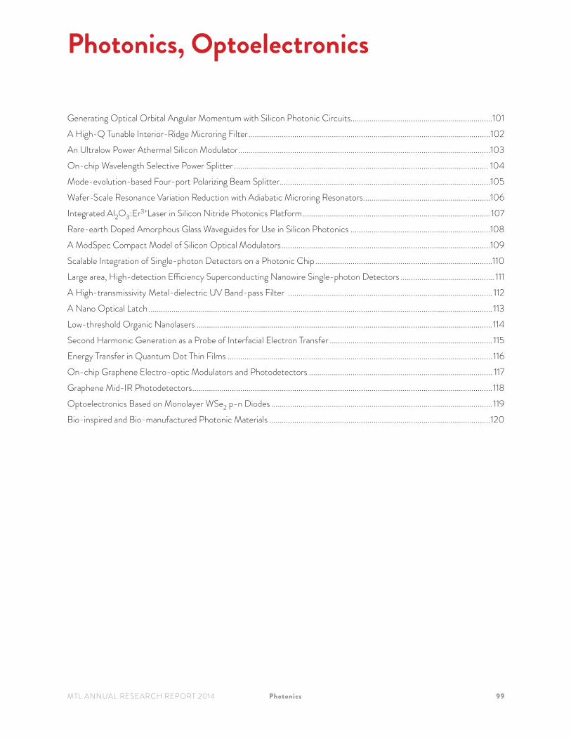
Figure 1(a) shows a scanning-electron micrograph (SEM) of the fabricated silicon PIC, which is essentially an optical phased array in which the emitting phase
of each optical antenna depends on its azimuthal angle θ, as shown in Figure 1(a) where a phase profile exp(j⋅l⋅θ) is coded to generate an OAM with l=3. Unlike conventional phased arrays where a rectangular layout is used, the 180 optical antennas here are placed within a circle to reflect the circular symmetry of the OAM beam. Figure 1(b) shows the measured near field where uniform emission across all of the 180 optical emitters was observed. The measured far field is shown in Figure 1(d), agreeing well with the simulation in Figure 1(c). Multiple interference orders are seen in the far field since the antenna spacing (9μm) is a multiple of the optical wavelength (1.55μm). The multiple OAM beams can be used, for example, to optically trap and rotate multiple particles simultaneously. By coding the array with different phase profiles, optical beams with different OAM states (l=±1 and ±3) were also generated (Figure 3(e)). All of the generated far-field beams have zero intensity in the center, representing a phase singularity, which is the signature of optical vortices.
▲Figure 1: (a) An SEM of the fabricated integrated photonic circuit coded with angular phase profile to generate OAM with l=3. (b) Measured near-field emission. (c) Simulated and (d) measured far-field pattern with l=3. (e) OAMs with l=±1 and ±3 are generated (only one interference order is shown in the far field).
FURTHER READING
• T. Su, et al, “Demonstration of free space coherent optical communication using integrated silicon photonic orbital angular momentum devices,” Optical Express, vol. 20, pp. 9396-9402, 2012.
• J. Sun, et al, “Generating and Identifying Optical Orbital Angular Momentum with Silicon Photonic Circuits,” CLEO Postdeadline, 2014.
102 Photonics MTL ANNUAL RESEARCH REPORT 2014
A High-Q Tunable Interior-Ridge Microring FilterE. Timurdogan, Z. Su, J. Sun, M. Moresco, G. Leake D.D. Coolbaugh, M.R. Watts Sponsorship: DARPA MTO
Silicon photonics enables wavelength division multi-plexed (WDM) networks to be efficiently and cost-ef-fectively implemented on chips with potential for multi-terabit/s communication links. The multiplex-ing and demultiplexing operations are performed by microring-based filters, which require tight alignment between the laser comb and filter resonances. Howev-er, the alignment will be distorted due to wafer-scale dimensional errors and the temperature fluctuations, necessitating high-speed active thermo-optic control of microring filters. The challenge is to implement such control efficiently and rapidly to enable reconfigurable networks as well as track the dynamic processor ac-tivity. For this purpose, metal and silicon heaters have been implemented. The metal heaters, buried in or placed over the SiO2 cladding, achieve the highest tem-perature change within the metal and not inside the silicon core. This indirect heating method limits the thermal tuning efficiency and speed while increasing thermal crosstalk. On the contrary, the silicon heaters,
formed using ion implantation and directly integrated within the silicon microring, enable direct, efficient, and high-speed tuning due to the combination of lower heat capacity and reduced thermal conductance. How-ever, past silicon heater based tunable rings have suf-fered from increased optical losses due to the coupling geometry.
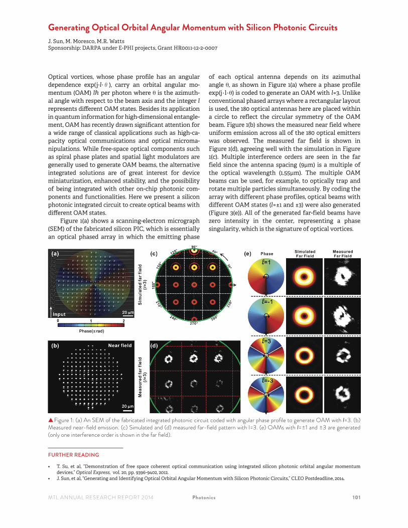
In this work, we demonstrate an interior-ridge microring resonator with a novel optical and electrical design that eliminates the aforementioned drawbacks of tunable filters with directly integrated silicon heaters (Figure 1-a). The 3-µm radius interior ridge microring resonator demonstrates a quality factor of 1.5×10⁵, limited mainly by the line edge roughness, while achieving a low-resistance (1kΩ) integrated silicon heater with a thermal tuning efficiency of 5.5µW/GHz (Figure 1-b). The resonator is used to operate as a 75GHz 3dB bandwidth filter. The filter demonstrates a record low insertion loss <0.05dB, owing to its high internal quality factor, over an uncorrupted 35-nm (4THz) free-spectral range.
▲Figure 1: a- Designed (3D-sketch) and fabricated (scanning-electron-microscopy image) optical tunable silicon modulators are shown to illustrate lossless (no optical overlap to doped regions) single mode operation. Heater is formed within filter using ion implantation (p and p+ doped silicon). b- Integrated optical filter is tuned over entire L-band (1565 nm-1600 nm) with as little as a ~4V drive voltage (20mW heater power).
FURTHER READING
• E. Timurdogan, Z. Su, J. Sun, M. Moresco, G. Leake, D. D. Coolbaugh, and M. R. Watts, “A High-Q Tunable Interior-Ridge Microring Filter,” in Proc. Conf. Lasers Electro-Opt (CLEO) , 8-13 June 2014., paper SF20.3
• E. Timurdogan, E. S. Hosseini, G. Leake, D. D. Coolbaugh, and M. R. Watts, “L-Shaped Resonant Microring (LRM) Filter with Integrated Thermal Tuner,” in Proc. Conf. Lasers Electro-Opt. (CLEO), 2013, paper CTh4F.2.
• M. Watts, W. Zortman, D. Trotter, G. Nielson, D. Luck, and R. Young, “Adiabatic Resonant Microrings (ARMs) with Directly Integrated Thermal Microphotonics,” in Proc. Conf. Lasers Electro-Opt. (CLEO), 2009, paper CPDB10.
MTL ANNUAL RESEARCH REPORT 2014 Photonics 103
An Ultralow Power Athermal Silicon ModulatorE. Timurdogan, C. Sorace-Agaskar, J. Sun, E. Hosseini, A. Biberman, M.R. Watts Sponsorship: DARPA MTO
On- and off-chip interconnects, traditionally executed using parallel electrical links, are struggling to satisfy the current bandwidth, density, power consumption and cost requirements of the computing and commu-nication industries. These limitations are becoming ap-parent in rapidly scaling massively parallel computing systems such as data centers for cloud computing and high-performance “supercomputers” used for large-scale scientific computation. Silicon photonics has emerged as the leading candidate for implementing ultralow power communication networks in high-performance computers, yet current components (lasers, modulators, filters, and detectors) consume too much power for the high-speed femtojoule-class links that ultimately will be required. In this work, we demonstrate and characterize
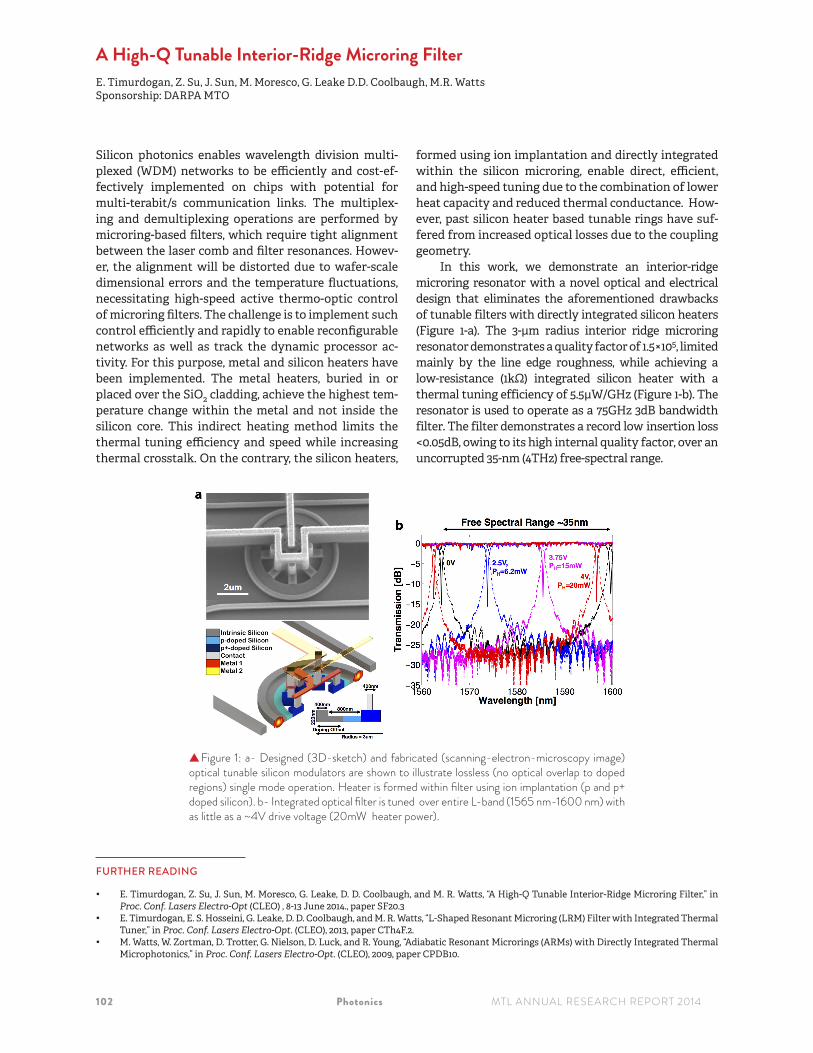
the first modulator to achieve simultaneous high-speed (25 Gb/s), low-voltage (0.5 VPP) and efficient 0.9 fJ per bit error-free operation. This low-energy high-speed oper-ation is enabled by a record electro-optic response, ob-tained in a vertical p–n junction device that at 250 pm/V (30 GHz/V) is up to 10 times larger than prior demon-strations. In addition, this record electro-optic response is used to compensate for thermal drift over a 7.5°C temperature range with little additional energy con-sumption (0.24 fJ per bit for a total energy consumption below 1.03 J per bit). The combined results (see Figure 1) of highly efficient modulation and electro-optic thermal compensation represent a new paradigm in modulator development and a major step towards single-digit fem-tojoule-class communications.
▲Figure 1: a- Scanning-electron-microscopy image of optical microdisk modulator illustrates circular contacts and short interconnects. b- Athermal operation over 10°C temperature range is realized by changing only modula-tor DC bias (consuming <1fJ/bit tuning energy). c- The 15- 20- and 25Gb/s transmissions from the optical mod-ulator are taken from a digital communication analyzer, consuming only <1fJ/bit modulation energy. The 44-Gb/s transmission of same optical modulator was possible at higher modulation energy.
FURTHER READING
• E. Timurdogan, C. M. Sorace-Agaskar, J. Sun, E. S. Hosseini and M. R. Watts , “An ultralow power athermal silicon modulator,” Nature Communications 5, no. 4008, 2013.
104 Photonics MTL ANNUAL RESEARCH REPORT 2014
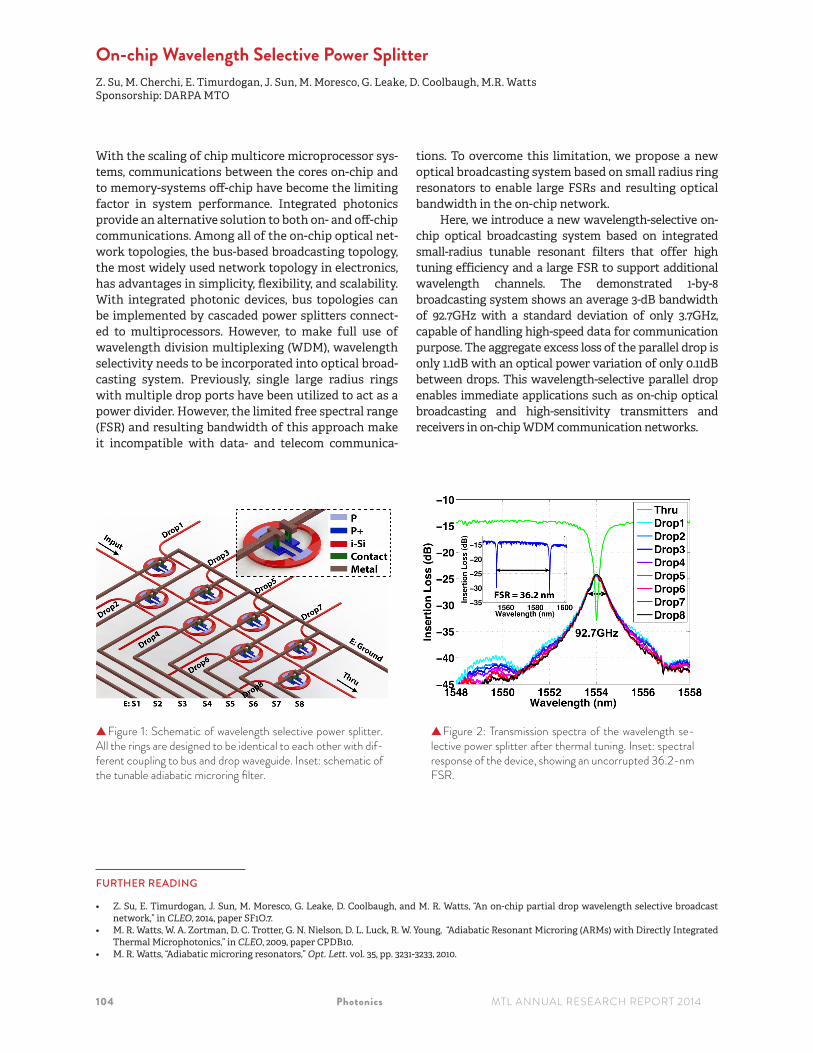
On-chip Wavelength Selective Power SplitterZ. Su, M. Cherchi, E. Timurdogan, J. Sun, M. Moresco, G. Leake, D. Coolbaugh, M.R. Watts Sponsorship: DARPA MTO
With the scaling of chip multicore microprocessor sys-tems, communications between the cores on-chip and to memory-systems off-chip have become the limiting factor in system performance. Integrated photonics provide an alternative solution to both on- and off-chip communications. Among all of the on-chip optical net-work topologies, the bus-based broadcasting topology, the most widely used network topology in electronics, has advantages in simplicity, flexibility, and scalability. With integrated photonic devices, bus topologies can be implemented by cascaded power splitters connect-ed to multiprocessors. However, to make full use of wavelength division multiplexing (WDM), wavelength selectivity needs to be incorporated into optical broad-casting system. Previously, single large radius rings with multiple drop ports have been utilized to act as a power divider. However, the limited free spectral range (FSR) and resulting bandwidth of this approach make it incompatible with data- and telecom communica-
tions. To overcome this limitation, we propose a new optical broadcasting system based on small radius ring resonators to enable large FSRs and resulting optical bandwidth in the on-chip network.
Here, we introduce a new wavelength-selective on-chip optical broadcasting system based on integrated small-radius tunable resonant filters that offer high tuning efficiency and a large FSR to support additional wavelength channels. The demonstrated 1-by-8 broadcasting system shows an average 3-dB bandwidth of 92.7GHz with a standard deviation of only 3.7GHz, capable of handling high-speed data for communication purpose. The aggregate excess loss of the parallel drop is only 1.1dB with an optical power variation of only 0.11dB between drops. This wavelength-selective parallel drop enables immediate applications such as on-chip optical broadcasting and high-sensitivity transmitters and receivers in on-chip WDM communication networks.
▲Figure 1: Schematic of wavelength selective power splitter. All the rings are designed to be identical to each other with dif-ferent coupling to bus and drop waveguide. Inset: schematic of the tunable adiabatic microring filter.
▲Figure 2: Transmission spectra of the wavelength se-lective power splitter after thermal tuning. Inset: spectral response of the device, showing an uncorrupted 36.2-nm FSR.
FURTHER READING
• Z. Su, E. Timurdogan, J. Sun, M. Moresco, G. Leake, D. Coolbaugh, and M. R. Watts, “An on-chip partial drop wavelength selective broadcast network,” in CLEO, 2014, paper SF1O.7.
• M. R. Watts, W. A. Zortman, D. C. Trotter, G. N. Nielson, D. L. Luck, R. W. Young, “Adiabatic Resonant Microring (ARMs) with Directly Integrated Thermal Microphotonics,” in CLEO, 2009, paper CPDB10.
• M. R. Watts, “Adiabatic microring resonators,” Opt. Lett. vol. 35, pp. 3231-3233, 2010.
MTL ANNUAL RESEARCH REPORT 2014 Photonics 105
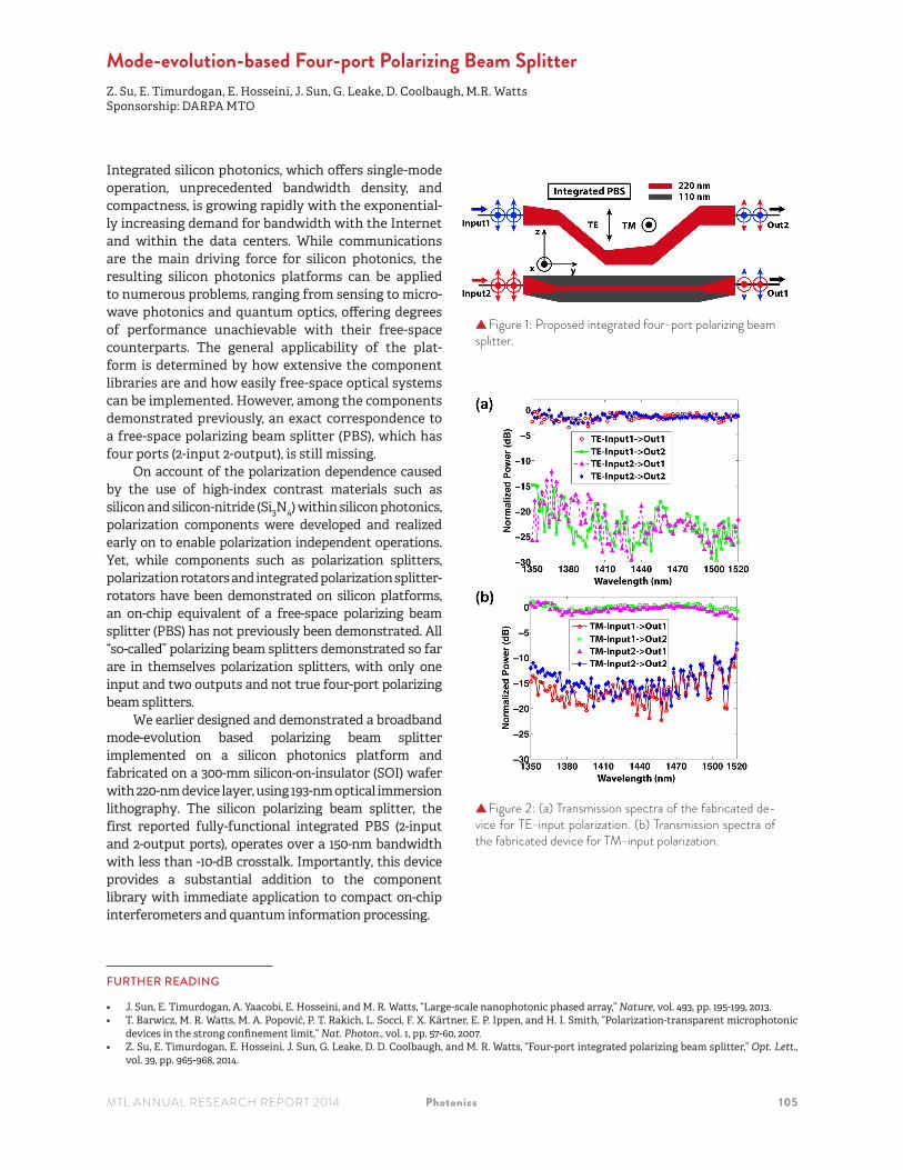
Mode-evolution-based Four-port Polarizing Beam SplitterZ. Su, E. Timurdogan, E. Hosseini, J. Sun, G. Leake, D. Coolbaugh, M.R. Watts Sponsorship: DARPA MTO
Integrated silicon photonics, which offers single-mode operation, unprecedented bandwidth density, and compactness, is growing rapidly with the exponential-ly increasing demand for bandwidth with the Internet and within the data centers. While communications are the main driving force for silicon photonics, the resulting silicon photonics platforms can be applied to numerous problems, ranging from sensing to micro-wave photonics and quantum optics, offering degrees of performance unachievable with their free-space counterparts. The general applicability of the plat-form is determined by how extensive the component libraries are and how easily free-space optical systems can be implemented. However, among the components demonstrated previously, an exact correspondence to a free-space polarizing beam splitter (PBS), which has four ports (2-input 2-output), is still missing.
On account of the polarization dependence caused by the use of high-index contrast materials such as silicon and silicon-nitride (Si3N4) within silicon photonics, polarization components were developed and realized early on to enable polarization independent operations. Yet, while components such as polarization splitters, polarization rotators and integrated polarization splitter-rotators have been demonstrated on silicon platforms, an on-chip equivalent of a free-space polarizing beam splitter (PBS) has not previously been demonstrated. All “so-called” polarizing beam splitters demonstrated so far are in themselves polarization splitters, with only one input and two outputs and not true four-port polarizing beam splitters.
We earlier designed and demonstrated a broadband mode-evolution based polarizing beam splitter implemented on a silicon photonics platform and fabricated on a 300-mm silicon-on-insulator (SOI) wafer with 220-nm device layer, using 193-nm optical immersion lithography. The silicon polarizing beam splitter, the first reported fully-functional integrated PBS (2-input and 2-output ports), operates over a 150-nm bandwidth with less than -10-dB crosstalk. Importantly, this device provides a substantial addition to the component library with immediate application to compact on-chip interferometers and quantum information processing.
▲Figure 2: (a) Transmission spectra of the fabricated de-vice for TE-input polarization. (b) Transmission spectra of the fabricated device for TM-input polarization.
FURTHER READING
• J. Sun, E. Timurdogan, A. Yaacobi, E. Hosseini, and M. R. Watts, “Large-scale nanophotonic phased array,” Nature, vol. 493, pp. 195-199, 2013.• T. Barwicz, M. R. Watts, M. A. Popović, P. T. Rakich, L. Socci, F. X. Kärtner, E. P. Ippen, and H. I. Smith, “Polarization-transparent microphotonic
devices in the strong confinement limit,” Nat. Photon., vol. 1, pp. 57-60, 2007.• Z. Su, E. Timurdogan, E. Hosseini, J. Sun, G. Leake, D. D. Coolbaugh, and M. R. Watts, “Four-port integrated polarizing beam splitter,” Opt. Lett.,
vol. 39, pp. 965-968, 2014.
106 Photonics MTL ANNUAL RESEARCH REPORT 2014
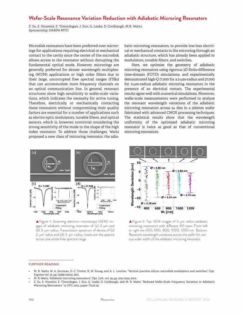
Wafer-Scale Resonance Variation Reduction with Adiabatic Microring ResonatorsZ. Su, E. Hosseini, E. Timurdogan, J. Sun, G. Leake, D. Coolbaugh, M.R. Watts Sponsorship: DARPA MTO
Microdisk resonators have been preferred over micror-ings for applications requiring electrical or mechanical contact to the cavity since the center of the microdisk allows access to the resonator without disrupting the fundamental optical mode. However, microrings are generally preferred for denser wavelength multiplex-ing (WDM) applications or high order filters due to their large, uncorrupted free spectral ranges (FSRs) that can accommodate more frequency channels on an optical communication line. In general, resonant structures show high sensitivity to wafer-scale varia-tions, which indicates the necessity for active tuning. Therefore, electrically or mechanically contacting these resonators without compromising their quality factors are essential for a number of applications such as electro-optic modulators, tunable filters, and optical sensors, which is, however, nontrivial considering the strong sensitivity of the mode to the shape of the high index resonator. To address those challenges, Watts proposed a new class of microring resonator, the adia-
batic microring resonators, to provide low-loss electri-cal or mechanical contacts to the microring through an adiabatic structure, which has already been applied to modulators, tunable filters, and switches.
Here, we optimize the geometry of adiabatic microring resonators using rigorous 3D finite-difference time-domain (FDTD) simulations, and experimentally demonstrated high-Q (7,000 for a 2-μm-radius and 27,000 for 3-μm-radius) adiabatic microring resonators in the presence of an electrical contact. The experimental results agree well with numerical simulations. Moreover, wafer-scale measurements were performed to analyze the resonant wavelength variations of the adiabatic microring resonators across 54 dies in a 300mm wafer fabricated with advanced CMOS processing techniques. The statistical results show that the wavelength uniformity of the optimized adiabatic microring resonator is twice as good as that of conventional microring resonators.
▲Figure 1: Scanning-electron-microscope (SEM) im-ages of adiabatic microring resonator of (a) 2-μm and (b) 3-μm radius. Transmission spectrum of device of (c) 2-μm radius and (d) 3-μm radius. Insets are the spectra across one whole free spectral range.
▲Figure 2: Top: SEM images of 3-μm radius adiabatic microring resonators with different W2 sizes. From left to right are 400, 600, 800, 1000, 1200 nm. Bottom: Resonant wavelength variations across the wafer for vari-ous wider width of the adiabatic microring resonator.
FURTHER READING
• M. R. Watts, W. A. Zortman, D. C. Trotter, R. W. Young, and A. L. Lentine, “Vertical junction silicon microdisk modulators and switches,” Opt. Express vol. 19, pp. 21989-22003, 2011.
• M. R. Watts, “Adiabatic microring resonators,” Opt. Lett. vol. 35, pp. 3231-3233, 2010.• Z. Su, E. Hosseini, E. Timurdogan, J. Sun, G. Leake, D. Coolbaugh, and M. R. Watts, “Reduced Wafer-Scale Frequency Variation in Adiabatic
Microring Resonators,” in OFC, 2014, paper Th2A.55.
MTL ANNUAL RESEARCH REPORT 2014 Photonics 107
Integrated Al2O3:Er3+Laser in Silicon Nitride Photonics PlatformP. Purnawirman, A. Baldycheva, E.S. Hosseini, J.D.B. Bradley, M. Moresco, Z. Su, T. Adam, G. Leake, D. Coolbaugh, M.R. WattsSponsorship: DARPA E-Phi program (grant no. HR0011-12-2-0007),Samsung GRO program
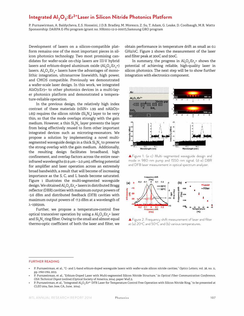
Development of lasers on a silicon-compatible plat-form remains one of the most important pieces in sil-icon photonics technology. Two most promising can-didates for wafer-scale on-chip lasers are III-V hybrid lasers and erbium-doped aluminum oxide (Al2O3:Er3+) lasers. Al2O3:Er3+ lasers have the advantages of mono-lithic integration, ultranarrow linewidth, high power, and CMOS compatible. Previously we demonstrated a wafer-scale laser design. In this work, we integrated Al2O3:Er3+ to other photonics devices in a multi-lay-er photonics platform and demonstrated a tempera-ture-reliable operation.
In the previous design, the relatively high index contrast of these materials (nSiN= 1.99 and nAl2O3= 1.65) requires the silicon nitride (Si3N4) layer to be very thin, so that the mode overlaps strongly with the gain medium. However, a thin Si3N4 layer prevents the layer from being effectively reused to form other important integrated devices such as microring-resonators. We propose a solution by implementing a novel multi-segmented waveguide design in a thick Si3N4 to preserve the strong overlap with the gain medium. Additionally, the resulting design facilitates broadband, high confinement, and overlap factors across the entire near-infrared wavelengths (0.9 μm – 2.0 μm), offering potential for amplifier and laser operation across an extremely broad bandwidth, a result that will become of increasing importance as the S, C, and L bands become saturated. Figure 1 illustrates the multi-segmented waveguide design. We obtained Al2O3:Er3+ lasers in distributed Bragg reflector (DBR) cavities with maximum output powers of -3.6 dBm and distributed feedback (DFB) cavities with maximum output powers of -7.3 dBm at a wavelength of λ~1565nm.
Further, we propose a temperature-control free optical transceiver operation by using a Al2O3:Er3+ laser and Si3N4 ring filter. Owing to the small and almost equal thermo-optic coefficient of both the laser and filter, we
obtain performance in temperature drift as small as 0.1 GHz/oC. Figure 2 shows the measurement of the laser and filter peak at 20oC and 50oC.
In summary, the progress in Al2O3:Er3+ shows the potential of achieving reliable, high-quality laser in silicon photonics. The next step will be to show further integration with electronics component.
▲Figure 1: (a-c) Multi-segmented waveguide design and mode in 980-nm pump and 1550-nm signal. (d-e) DBR and DFB laser measurement in optical spectrum analyzer.
▲Figure 2: Frequency shift measurement of laser and filter at (a) 20oC and 50oC and (b) various temperatures.
FURTHER READING
• P. Purnawirman, et al., “C- and L-band erbium-doped waveguide lasers with wafer-scale silicon nitride cavities,” Optics Letters, vol. 38, no. 11, pp. 1760-1762, 2013.
• P. Purnawirman, et al., “Erbium-Doped Laser with Multi-segmented Silicon Nitride Structure,” in Optical Fiber Communication Conference, OSA Technical Digest (online) (Optical Society of America, 2014), paper W4E.5.
• P. Purnawirman, et al., “Integrated Al2O3:Er3+ DFB Laser for Temperature Control Free Operation with Silicon Nitride Ring,” to be presented at CLEO 2014, San Jose, CA, June, 2014).
108 Photonics MTL ANNUAL RESEARCH REPORT 2014
Rare-earth Doped Amorphous Glass Waveguides for Use in Silicon PhotonicsE.S. Magden, Purnawirman, C.M. Sorace-Agaskar, E.S. Hosseini, G. Petrich, M. Watts, L. Kolodziejski Sponsorship: DARPA
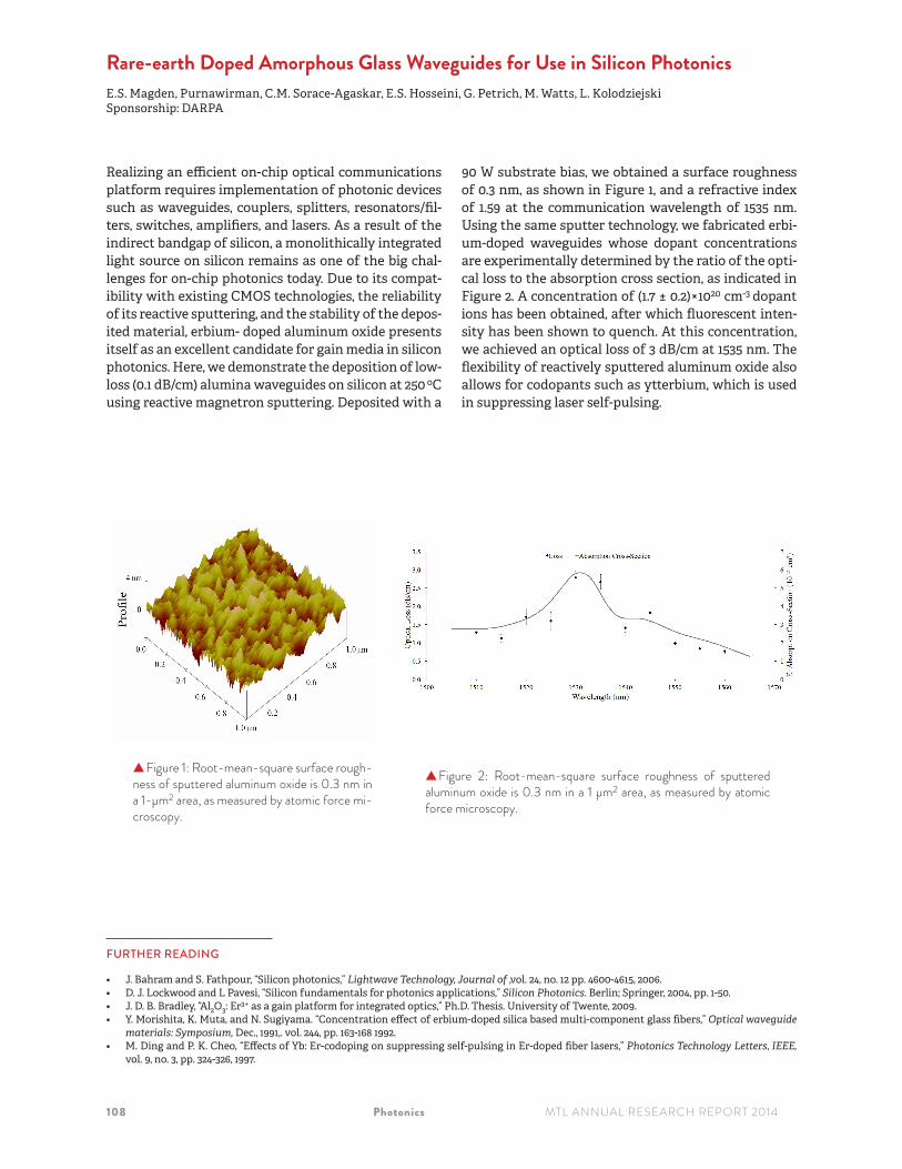
Realizing an efficient on-chip optical communications platform requires implementation of photonic devices such as waveguides, couplers, splitters, resonators/fil-ters, switches, amplifiers, and lasers. As a result of the indirect bandgap of silicon, a monolithically integrated light source on silicon remains as one of the big chal-lenges for on-chip photonics today. Due to its compat-ibility with existing CMOS technologies, the reliability of its reactive sputtering, and the stability of the depos-ited material, erbium- doped aluminum oxide presents itself as an excellent candidate for gain media in silicon photonics. Here, we demonstrate the deposition of low-loss (0.1 dB/cm) alumina waveguides on silicon at 250 oC using reactive magnetron sputtering. Deposited with a
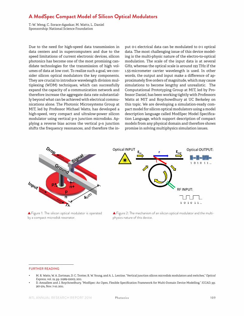
90 W substrate bias, we obtained a surface roughness of 0.3 nm, as shown in Figure 1, and a refractive index of 1.59 at the communication wavelength of 1535 nm. Using the same sputter technology, we fabricated erbi-um-doped waveguides whose dopant concentrations are experimentally determined by the ratio of the opti-cal loss to the absorption cross section, as indicated in Figure 2. A concentration of (1.7 ± 0.2)×1020 cm-3 dopant ions has been obtained, after which fluorescent inten-sity has been shown to quench. At this concentration, we achieved an optical loss of 3 dB/cm at 1535 nm. The flexibility of reactively sputtered aluminum oxide also allows for codopants such as ytterbium, which is used in suppressing laser self-pulsing.
▲Figure 1: Root-mean-square surface rough-ness of sputtered aluminum oxide is 0.3 nm in a 1-μm2 area, as measured by atomic force mi-croscopy.
▲Figure 2: Root-mean-square surface roughness of sputtered aluminum oxide is 0.3 nm in a 1 μm2 area, as measured by atomic force microscopy.
FURTHER READING
• J. Bahram and S. Fathpour, “Silicon photonics,” Lightwave Technology, Journal of ,vol. 24, no. 12 pp. 4600-4615, 2006.• D. J. Lockwood and L Pavesi, “Silicon fundamentals for photonics applications,” Silicon Photonics. Berlin; Springer, 2004, pp. 1-50.• J. D. B. Bradley, “Al2O3: Er3+ as a gain platform for integrated optics,” Ph.D. Thesis. University of Twente, 2009.• Y. Morishita, K. Muta, and N. Sugiyama. “Concentration effect of erbium-doped silica based multi-component glass fibers,” Optical waveguide
materials: Symposium, Dec., 1991,. vol. 244, pp. 163-168 1992.• M. Ding and P. K. Cheo, “Effects of Yb: Er-codoping on suppressing self-pulsing in Er-doped fiber lasers,” Photonics Technology Letters, IEEE,
vol. 9, no. 3, pp. 324-326, 1997.
MTL ANNUAL RESEARCH REPORT 2014 Photonics 109
A ModSpec Compact Model of Silicon Optical ModulatorsT.-W. Weng, C. Sorace-Agaskar, M. Watts, L. Daniel Sponsorship: National Science Foundation
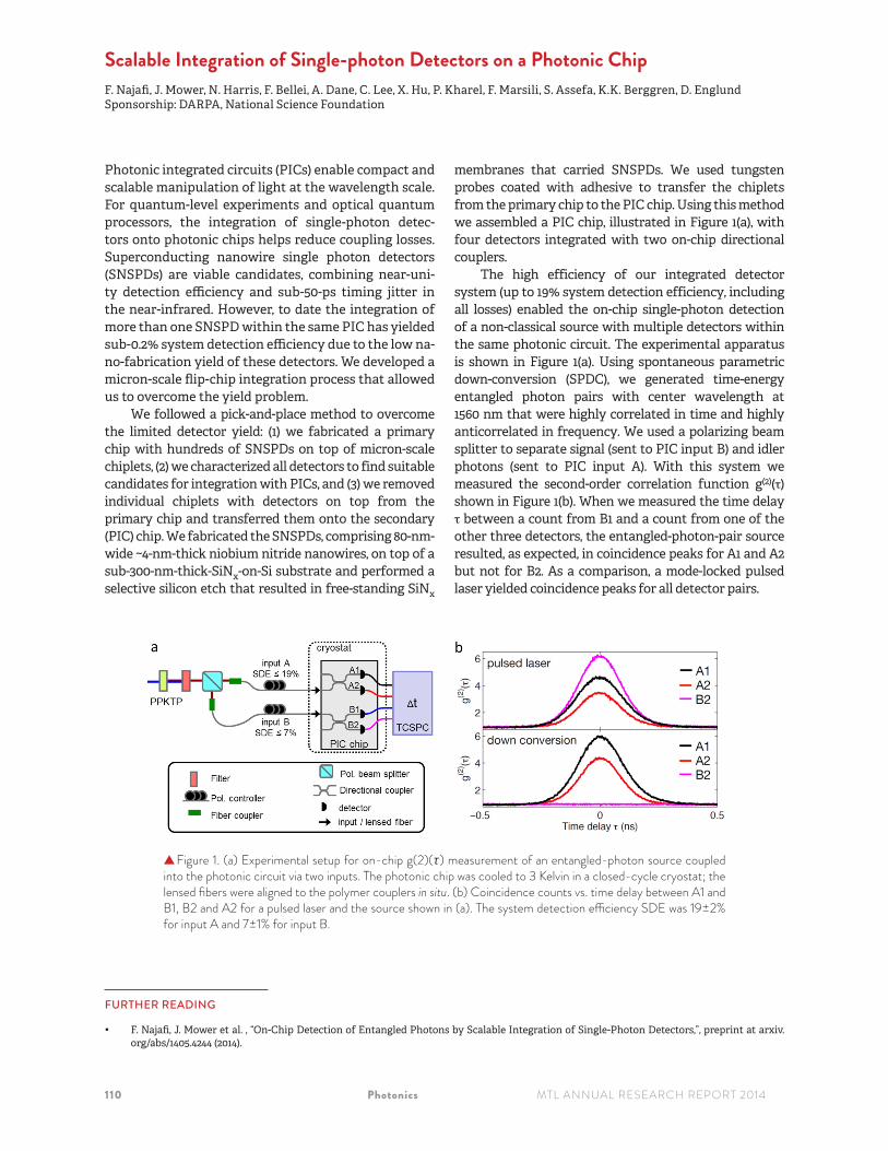
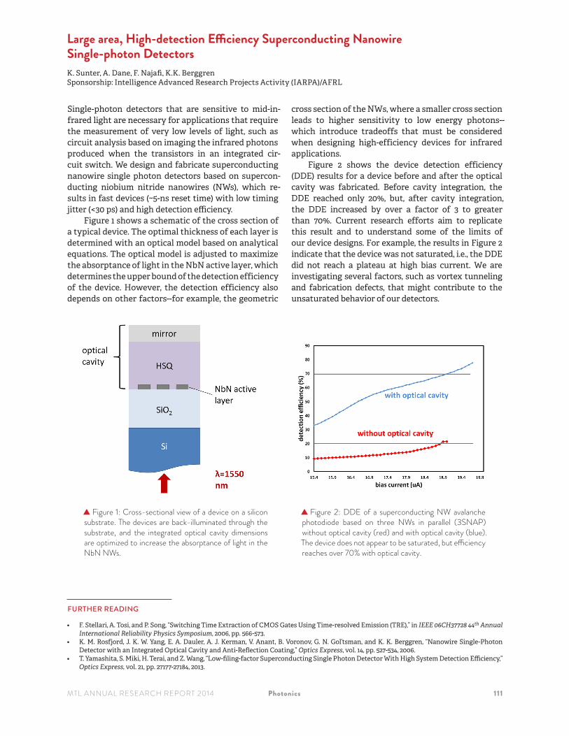
Due to the need for high-speed data transmission in data centers and in supercomputers and due to the speed limitations of current electronic devices, silicon photonics has become one of the most promising can-didate technologies for the transmission of high vol-umes of data at low cost. To realize such a goal, we con-sider silicon optical modulators the key components. They are crucial to introduce wavelength division mul-tiplexing (WDM) techniques, which can successfully expand the capacity of a communication network and therefore increase the aggregate data rate substantial-ly beyond what can be achieved with electrical commu-nications alone. The Photonic Microsystems Group at MIT, led by Professor Michael Watts, has developed a high-speed, very compact and ultralow-power silicon modulator using vertical p-n junction microdisks. Ap-plying a reverse bias across the vertical p-n junction shifts the frequency resonances, and therefore the in-
put 0-1 electrical data can be modulated to 0-1 optical data. The most challenging issue of this device model-ing is the multi-physic nature of the electro-to-optical modulation. The scale of the input data is at several GHz, whereas the optical scale is around 193 THz if the 1.55-micrometer carrier wavelength is used. In other words, the output and input make a difference of ap-proximately five orders of magnitude, which may cause simulations to become lengthy and unrealistic. The Computational Prototyping Group at MIT, led by Pro-fessor Daniel, has been working tightly with Professors Watts at MIT and Roychowdhury at UC Berkeley on this topic. We are developing a simulation-ready com-pact model for silicon optical modulators using a model description language called ModSpec Model Specifica-tion Language, which support description of compact models from any physical domain and therefore shows promise in solving multiphysics simulation issues.
▲Figure 1: The silicon optical modulator is operated by a compact microdisk resonator.
▲Figure 2: The mechanism of an silicon optical modulator and the multi-physics nature of this device.
FURTHER READING
• M. R. Watts, W. A. Zortman, D. C. Trotter, R. W. Young, and A. L. Lentine, “Vertical junction silicon microdisk modulators and switches,” Optical Express, vol. 19, pp. 21989-22003, 2011.
• D. Amsallem and J. Roychowdhury, “ModSpec: An Open, Flexible Specification Framework for Multi-Domain Device Modelling,” ICCAD, pp. 367-374, Nov. 7-10, 2011.
110 Photonics MTL ANNUAL RESEARCH REPORT 2014
Scalable Integration of Single-photon Detectors on a Photonic ChipF. Najafi, J. Mower, N. Harris, F. Bellei, A. Dane, C. Lee, X. Hu, P. Kharel, F. Marsili, S. Assefa, K.K. Berggren, D. EnglundSponsorship: DARPA, National Science Foundation
Photonic integrated circuits (PICs) enable compact and scalable manipulation of light at the wavelength scale. For quantum-level experiments and optical quantum processors, the integration of single-photon detec-tors onto photonic chips helps reduce coupling losses. Superconducting nanowire single photon detectors (SNSPDs) are viable candidates, combining near-uni-ty detection efficiency and sub-50-ps timing jitter in the near-infrared. However, to date the integration of more than one SNSPD within the same PIC has yielded sub-0.2% system detection efficiency due to the low na-no-fabrication yield of these detectors. We developed a micron-scale flip-chip integration process that allowed us to overcome the yield problem.
We followed a pick-and-place method to overcome the limited detector yield: (1) we fabricated a primary chip with hundreds of SNSPDs on top of micron-scale chiplets, (2) we characterized all detectors to find suitable candidates for integration with PICs, and (3) we removed individual chiplets with detectors on top from the primary chip and transferred them onto the secondary (PIC) chip. We fabricated the SNSPDs, comprising 80-nm-wide ~4-nm-thick niobium nitride nanowires, on top of a sub-300-nm-thick-SiNx-on-Si substrate and performed a selective silicon etch that resulted in free-standing SiNx
membranes that carried SNSPDs. We used tungsten probes coated with adhesive to transfer the chiplets from the primary chip to the PIC chip. Using this method we assembled a PIC chip, illustrated in Figure 1(a), with four detectors integrated with two on-chip directional couplers.
The high efficiency of our integrated detector system (up to 19% system detection efficiency, including all losses) enabled the on-chip single-photon detection of a non-classical source with multiple detectors within the same photonic circuit. The experimental apparatus is shown in Figure 1(a). Using spontaneous parametric down-conversion (SPDC), we generated time-energy entangled photon pairs with center wavelength at 1560 nm that were highly correlated in time and highly anticorrelated in frequency. We used a polarizing beam splitter to separate signal (sent to PIC input B) and idler photons (sent to PIC input A). With this system we measured the second-order correlation function g(2)(τ) shown in Figure 1(b). When we measured the time delayτ between a count from B1 and a count from one of the other three detectors, the entangled-photon-pair source resulted, as expected, in coincidence peaks for A1 and A2 but not for B2. As a comparison, a mode-locked pulsed laser yielded coincidence peaks for all detector pairs.
▲Figure 1. (a) Experimental setup for on-chip g(2)(τ) measurement of an entangled-photon source coupled into the photonic circuit via two inputs. The photonic chip was cooled to 3 Kelvin in a closed-cycle cryostat; the lensed fibers were aligned to the polymer couplers in situ. (b) Coincidence counts vs. time delay between A1 and B1, B2 and A2 for a pulsed laser and the source shown in (a). The system detection efficiency SDE was 19±2% for input A and 7±1% for input B.
FURTHER READING
• F. Najafi, J. Mower et al. , “On-Chip Detection of Entangled Photons by Scalable Integration of Single-Photon Detectors,”, preprint at arxiv.org/abs/1405.4244 (2014).
MTL ANNUAL RESEARCH REPORT 2014 Photonics 111
Large area, High-detection Efficiency Superconducting Nanowire Single-photon DetectorsK. Sunter, A. Dane, F. Najafi, K.K. Berggren Sponsorship: Intelligence Advanced Research Projects Activity (IARPA)/AFRL
Single-photon detectors that are sensitive to mid-in-frared light are necessary for applications that require the measurement of very low levels of light, such as circuit analysis based on imaging the infrared photons produced when the transistors in an integrated cir-cuit switch. We design and fabricate superconducting nanowire single photon detectors based on supercon-ducting niobium nitride nanowires (NWs), which re-sults in fast devices (~5-ns reset time) with low timing jitter (<30 ps) and high detection efficiency.
Figure 1 shows a schematic of the cross section of a typical device. The optimal thickness of each layer is determined with an optical model based on analytical equations. The optical model is adjusted to maximize the absorptance of light in the NbN active layer, which determines the upper bound of the detection efficiency of the device. However, the detection efficiency also depends on other factors--for example, the geometric
cross section of the NWs, where a smaller cross section leads to higher sensitivity to low energy photons--which introduce tradeoffs that must be considered when designing high-efficiency devices for infrared applications.
Figure 2 shows the device detection efficiency (DDE) results for a device before and after the optical cavity was fabricated. Before cavity integration, the DDE reached only 20%, but, after cavity integration, the DDE increased by over a factor of 3 to greater than 70%. Current research efforts aim to replicate this result and to understand some of the limits of our device designs. For example, the results in Figure 2 indicate that the device was not saturated, i.e., the DDE did not reach a plateau at high bias current. We are investigating several factors, such as vortex tunneling and fabrication defects, that might contribute to the unsaturated behavior of our detectors.
▲ Figure 1: Cross-sectional view of a device on a silicon substrate. The devices are back-illuminated through the substrate, and the integrated optical cavity dimensions are optimized to increase the absorptance of light in the NbN NWs.
▲ Figure 2: DDE of a superconducting NW avalanche photodiode based on three NWs in parallel (3SNAP) without optical cavity (red) and with optical cavity (blue). The device does not appear to be saturated, but efficiency reaches over 70% with optical cavity.
FURTHER READING
• F. Stellari, A. Tosi, and P. Song, “Switching Time Extraction of CMOS Gates Using Time-resolved Emission (TRE),” in IEEE 06CH37728 44th Annual International Reliability Physics Symposium, 2006, pp. 566-573.
• K. M. Rosfjord, J. K. W. Yang, E. A. Dauler, A. J. Kerman, V. Anant, B. Voronov, G. N. Gol’tsman, and K. K. Berggren, “Nanowire Single-Photon Detector with an Integrated Optical Cavity and Anti-Reflection Coating,” Optics Express, vol. 14, pp. 527-534, 2006.
• T. Yamashita, S. Miki, H. Terai, and Z. Wang, “Low-filing-factor Superconducting Single Photon Detector With High System Detection Efficiency,” Optics Express, vol. 21, pp. 27177-27184, 2013.
112 Photonics MTL ANNUAL RESEARCH REPORT 2014
A High-transmissivity Metal-dielectric UV Band-pass Filter J. Mu, P.T. Lin, L. Zhang, J. Michel, L.C. Kimerling, F. Jaworski, A. Agarwal Sponsorship: Institute for Soldier Nanotechnologies
Ultraviolet (UV) technologies have found increasing importance in various applications including pollu-tion monitoring, flame detection, UV astronomy, and space-to-space communications. Due to the strong ab-sorption of sub-200-nm light by ozone and molecular oxygen in the terrestrial atmosphere, most practical technology development occurs in the mid-UV (200-300 nm) and near-UV (300-400 nm) ranges. To allow us to focus only on mid- and near-UV light, it is critical to obtain a solar-blind UV filter that blocks the visible and infrared portions of the solar spectrum.
For UV light detection, wide bandgap materials such as III-nitride based solar-blind UV photo detectors have been proposed and studied. Not all approaches are compatible with standard complementary metal oxide semiconductor (CMOS) fabrication processes; hence integration with silicon-based devices is challenging. Considering currently available mature and cheap silicon processing technologies, the integration of a solar-blind UV band-pass filter with a silicon-based UV photo detector is a solution for obtaining a low-cost and effective UV detector.
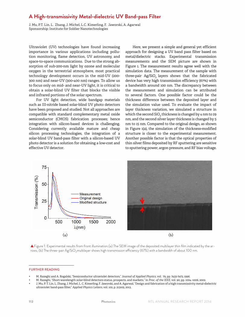
Here, we present a simple and general yet efficient approach for designing a UV band pass filter based on metal/dielectric stacks. Experimental transmission measurements and the SEM picture are shown in Figure 1. The measurement results agree well with the simulation data. The measurement of the sample with three-pair Ag/SiO2 layers shows that the fabricated device has very high transmission efficiency (67%) with a bandwidth around 100 nm. The discrepancy between the measurement and simulation can be attributed to several factors. One possible factor could be the thickness difference between the deposited layer and the simulation value used. To evaluate the impact of layer thickness variation, we simulated a structure in which the second SiO2 thickness is changed by 4 nm to 29 nm, and the second silver layer thickness is changed by 5 nm to 15 nm. Compared to the original design, as shown in Figure 1(a), the simulation of the thickness-modified structure is closer to the experimental measurement. Another possible factor is that the optical properties of thin silver films deposited by RF sputtering are sensitive to sputtering power, argon pressure, and RF bias voltage.
▲Figure 1: Experimental results from front illumination.(a) The SEM image of the deposited multilayer thin film indicated by the ar-rows; (b) The three-pair Ag/SiO2multilayer shows high transmission efficiency (67%) with a bandwidth of about 100 nm.
FURTHER READING
• M. Razeghi and A. Rogalski, “Semiconductor ultraviolet detectors,” Journal of Applied Physics, vol. 79, pp. 7433-7473, 1996.• M. Razeghi, “Short-wavelength solar-blind detectors-status, prospects, and markets,” in Proc. of the IEEE, vol. 90, pp. 1004 -1006, 2002.• J. Mu, P. T. Lin, L. Zhang, J. Michel, L. C. Kimerling, F. Jaworski, and A. Agarwal, “Design and fabrication of a high transmissivity metal-dielectric
A Nano Optical LatchJ. Mu, Z. Han, S Grillanda, A. Melloni, J. Michel, L.C. Kimerling, A. Agarwal
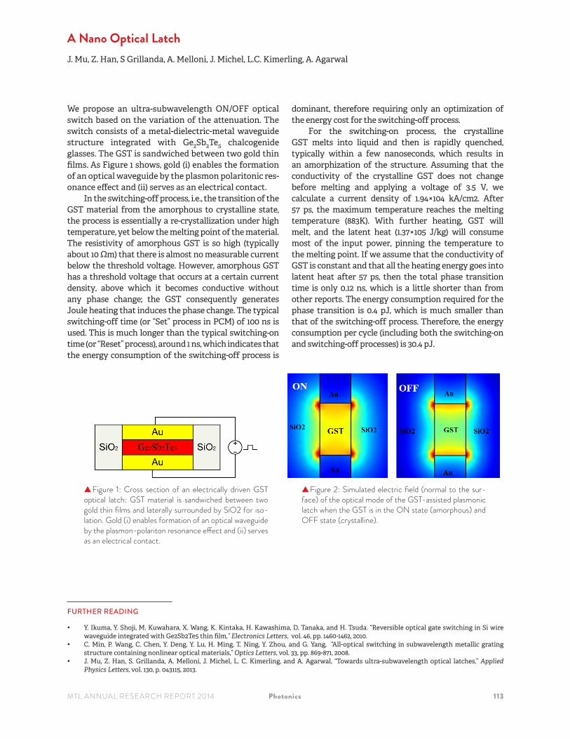
We propose an ultra-subwavelength ON/OFF optical switch based on the variation of the attenuation. The switch consists of a metal-dielectric-metal waveguide structure integrated with Ge2Sb2Te5 chalcogenide glasses. The GST is sandwiched between two gold thin films. As Figure 1 shows, gold (i) enables the formation of an optical waveguide by the plasmon polaritonic res-onance effect and (ii) serves as an electrical contact.
In the switching-off process, i.e., the transition of the GST material from the amorphous to crystalline state, the process is essentially a re-crystallization under high temperature, yet below the melting point of the material. The resistivity of amorphous GST is so high (typically about 10 Ωm) that there is almost no measurable current below the threshold voltage. However, amorphous GST has a threshold voltage that occurs at a certain current density, above which it becomes conductive without any phase change; the GST consequently generates Joule heating that induces the phase change. The typical switching-off time (or “Set” process in PCM) of 100 ns is used. This is much longer than the typical switching-on time (or “Reset” process), around 1 ns, which indicates that the energy consumption of the switching-off process is
dominant, therefore requiring only an optimization of the energy cost for the switching-off process.
For the switching-on process, the crystalline GST melts into liquid and then is rapidly quenched, typically within a few nanoseconds, which results in an amorphization of the structure. Assuming that the conductivity of the crystalline GST does not change before melting and applying a voltage of 3.5 V, we calculate a current density of 1.94×10⁴ kA/cm2. After 57 ps, the maximum temperature reaches the melting temperature (883K). With further heating, GST will melt, and the latent heat (1.37×10⁵ J/kg) will consume most of the input power, pinning the temperature to the melting point. If we assume that the conductivity of GST is constant and that all the heating energy goes into latent heat after 57 ps, then the total phase transition time is only 0.12 ns, which is a little shorter than from other reports. The energy consumption required for the phase transition is 0.4 pJ, which is much smaller than that of the switching-off process. Therefore, the energy consumption per cycle (including both the switching-on and switching-off processes) is 30.4 pJ.
▲Figure 1: Cross section of an electrically driven GST optical latch: GST material is sandwiched between two gold thin films and laterally surrounded by SiO2 for iso-lation. Gold (i) enables formation of an optical waveguide by the plasmon-polariton resonance effect and (ii) serves as an electrical contact.
▲Figure 2: Simulated electric field (normal to the sur-face) of the optical mode of the GST-assisted plasmonic latch when the GST is in the ON state (amorphous) and OFF state (crystalline).
FURTHER READING
• Y. Ikuma, Y. Shoji, M. Kuwahara, X. Wang, K. Kintaka, H. Kawashima, D. Tanaka, and H. Tsuda. “Reversible optical gate switching in Si wire waveguide integrated with Ge2Sb2Te5 thin film,” Electronics Letters, vol. 46, pp. 1460-1462, 2010.
• C. Min, P. Wang, C. Chen, Y. Deng, Y. Lu, H. Ming, T. Ning, Y. Zhou, and G. Yang, “All-optical switching in subwavelength metallic grating structure containing nonlinear optical materials,” Optics Letters, vol. 33, pp. 869-871, 2008.
• J. Mu, Z. Han, S. Grillanda, A. Melloni, J. Michel, L. C. Kimerling, and A. Agarwal, “Towards ultra-subwavelength optical latches,” Applied Physics Letters, vol. 130, p. 043115, 2013.
114 Photonics MTL ANNUAL RESEARCH REPORT 2014
Low-threshold Organic NanolasersT. Mahoney, V. Bulović
Since the first demonstration of lasing in organic gain media, there has been great interest in developing an electrically pumped organic laser. Organic lasers have been demonstrated using different device structures such as VCSELS, distributed feedback lasers, and pho-tonic crystal cavity lasers. However, none of these have achieved electrical pumping. Singlet triplet annihila-tion in the organics leads to unfeasibly large threshold current densities. To lower the threshold for organic la-sers, we have designed a cavity with a high quality fac-tor/mode volume (Q/V) ratio and a high spontaneous emission factor (b).
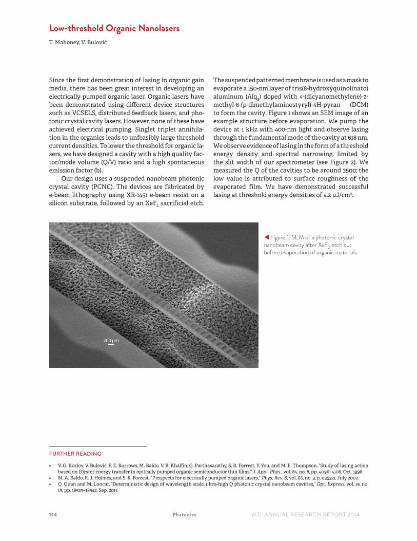
Our design uses a suspended nanobeam photonic crystal cavity (PCNC). The devices are fabricated by e-beam lithography using XR-1451 e-beam resist on a silicon substrate, followed by an XeF2 sacrificial etch.
The suspended patterned membrane is used as a mask to evaporate a 150-nm layer of tris(8-hydroxyquinolinato) aluminum (Alq3) doped with 4-(dicyanomethylene)-2-methyl-6-(p-dimethylaminostyryl)-4H-pyran (DCM) to form the cavity. Figure 1 shows an SEM image of an example structure before evaporation. We pump the device at 1 kHz with 400-nm light and observe lasing through the fundamental mode of the cavity at 618 nm. We observe evidence of lasing in the form of a threshold energy density and spectral narrowing, limited by the slit width of our spectrometer (see Figure 2). We measured the Q of the cavities to be around 3500; the low value is attributed to surface roughness of the evaporated film. We have demonstrated successful lasing at threshold energy densities of 4.2 uJ/cm2.
FURTHER READING
• V. G. Kozlov, V. Bulović, P. E. Burrows, M. Baldo, V. B. Khalfin, G. Parthasarathy, S. R. Forrest, Y. You, and M. E. Thompson, “Study of lasing action based on Förster energy transfer in optically pumped organic semiconductor thin films,” J. Appl. Phys., vol. 84, no. 8, pp. 4096–4108, Oct. 1998.
• M. A. Baldo, R. J. Holmes, and S. R. Forrest, “Prospects for electrically pumped organic lasers,” Phys. Rev. B, vol. 66, no. 3, p. 035321, July 2002.• Q. Quan and M. Loncar, “Deterministic design of wavelength scale, ultra-high Q photonic crystal nanobeam cavities,” Opt. Express, vol. 19, no.
19, pp. 18529–18542, Sep. 2011.
WFigure 1: SEM of a photonic crystal nanobeam cavity after XeF2 etch but before evaporation of organic materials.
MTL ANNUAL RESEARCH REPORT 2014 Photonics 115
Second Harmonic Generation as a Probe of Interfacial Electron TransferR.S. Hoffman, W.A. Tisdale Sponsorship: National Science Foundation, Department of Energy
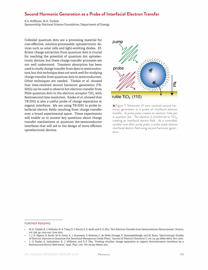
Colloidal quantum dots are a promising material for cost-effective, solution-processable optoelectronic de-vices such as solar cells and light-emitting diodes. Ef-ficient charge extraction from quantum dots is crucial for reaching the potential of quantum dot optoelec-tronic devices, but these charge transfer processes are not well understood. Transient absorption has been used to study charge transfer from dyes to semiconduc-tors, but this technique does not work well for studying charge transfer from quantum dots to semiconductors. Other techniques are needed. Tisdale et al. showed that time-resolved second harmonic generation (TR-SHG) can be used to observe hot electron transfer from PbSe quantum dots to the electron acceptor TiO2 with femtosecond time resolution. Kaake et al. showed that TR-SHG is also a useful probe of charge separation at organic interfaces. We are using TR-SHG to probe in-terfacial electric fields resulting from charge transfer over a broad experimental space. These experiments will enable us to answer key questions about charge transfer mechanisms at quantum dot-semiconductor interfaces that will aid in the design of more efficient optoelectronic devices.
▲Figure 1: Schematic of time-resolved second har-monic generation as a probe of interfacial electron transfer. A pump pulse creates an electron-hole pair in quantum dot. The electron is transferred to TiO2, creating an interfacial electric field. At a controlled, variable time after pump pulse, a probe pulse detects interfacial electric field using second harmonic gener-ation.
FURTHER READING
• W. A. Tisdale, K. J. Williams, B. A. Timp, D. J. Norris, E. S. Aydil, and X.-Y. Zhu, “Hot-Electron Transfer from Semiconductor Nanocrystals,” Science, vol. 328, pp. 1543-1547, June 2010.
• J. J. H. Pijpers, R. Koole, W. H. Evers, A. J. Houtepen, S. Boehme, C. de Mello Donegá, D. Vanmaekelbergh, and M. Bonn, “Spectroscopic Studies of Electron Injection in Quantum Dot Sensitized Mesoporous Oxide Films,” Journal of Physical Chemistry C, vol. 114, pp 18866-18873, Nov. 2010.
• L. G. Kaake, A. Jailaubekov, K. J. Williams, and X.-Y. Zhu, “Probing ultrafast charge separation at organic donor/acceptor interfaces by a femtosecond electric field meter,” Appl. Phys. Lett. Vol. 99, pp 083307, 2011.
116 Photonics MTL ANNUAL RESEARCH REPORT 2014
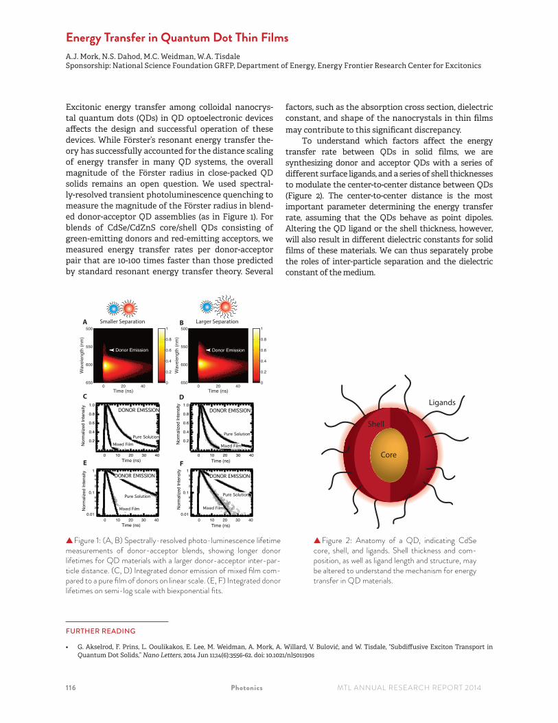
Energy Transfer in Quantum Dot Thin FilmsA.J. Mork, N.S. Dahod, M.C. Weidman, W.A. Tisdale Sponsorship: National Science Foundation GRFP, Department of Energy, Energy Frontier Research Center for Excitonics
Excitonic energy transfer among colloidal nanocrys-tal quantum dots (QDs) in QD optoelectronic devices affects the design and successful operation of these devices. While Förster’s resonant energy transfer the-ory has successfully accounted for the distance scaling of energy transfer in many QD systems, the overall magnitude of the Förster radius in close-packed QD solids remains an open question. We used spectral-ly-resolved transient photoluminescence quenching to measure the magnitude of the Förster radius in blend-ed donor-acceptor QD assemblies (as in Figure 1). For blends of CdSe/CdZnS core/shell QDs consisting of green-emitting donors and red-emitting acceptors, we measured energy transfer rates per donor-acceptor pair that are 10-100 times faster than those predicted by standard resonant energy transfer theory. Several
factors, such as the absorption cross section, dielectric constant, and shape of the nanocrystals in thin films may contribute to this significant discrepancy.
To understand which factors affect the energy transfer rate between QDs in solid films, we are synthesizing donor and acceptor QDs with a series of different surface ligands, and a series of shell thicknesses to modulate the center-to-center distance between QDs (Figure 2). The center-to-center distance is the most important parameter determining the energy transfer rate, assuming that the QDs behave as point dipoles. Altering the QD ligand or the shell thickness, however, will also result in different dielectric constants for solid films of these materials. We can thus separately probe the roles of inter-particle separation and the dielectric constant of the medium.
D
E
C
F
Time (ns)
Wav
elen
gth
(nm
)
0 20 40
500
550
600
650
Time (ns)
Wav
elen
gth
(nm
)
0 20 40
500
550
600
6500
0.2
0.4
0.6
0.8
1
0
0.2
0.4
0.6
0.8
1A B
Donor Emission Donor Emission
Smaller Separation Larger Separation
1.0
0.8
0.6
0.4
0.2Nor
mal
ized
Inte
nsity
403020100Time (ns)
0.012
46
0.12
46
1
Nor
mal
ized
Inte
nsity
403020100Time (ns)
1.0
0.8
0.6
0.4
0.2
Nor
mal
ized
Inte
nsity
403020100 Time (ns)
0.012
46
0.12
46
1
Nor
mal
ized
Inte
nsity
403020100 Time (ns)
Core
Shell
Ligands
▲Figure 1: (A, B) Spectrally-resolved photo-luminescence lifetime measurements of donor-acceptor blends, showing longer donor lifetimes for QD materials with a larger donor-acceptor inter-par-ticle distance. (C, D) Integrated donor emission of mixed film com-pared to a pure film of donors on linear scale. (E, F) Integrated donor lifetimes on semi-log scale with biexponential fits.
▲Figure 2: Anatomy of a QD, indicating CdSe core, shell, and ligands. Shell thickness and com-position, as well as ligand length and structure, may be altered to understand the mechanism for energy transfer in QD materials.
FURTHER READING
• G. Akselrod, F. Prins, L. Ooulikakos, E. Lee, M. Weidman, A. Mork, A. Willard, V. Bulović, and W. Tisdale, “Subdiffusive Exciton Transport in Quantum Dot Solids,” Nano Letters, 2014 Jun 11;14(6):3556-62. doi: 10.1021/nl501190s
MTL ANNUAL RESEARCH REPORT 2014 Photonics 117
On-chip Graphene Electro-optic Modulators and PhotodetectorsR.-J. Shiue, X. Gan, D. Englund Sponsorship: Energy Frontier Research Center for Excitonics
Graphene has shown great potential for compact opto-electronics with low power consumption. To increase the optical absorption in graphene, we have integrat-ed the material with silicon photonic waveguides and photonic crystal (PhC) cavities. In these structures, graphene stongly couples to the evanescent field of the waveguides and cavities, resulting in near-unity ab-sorption. Based on these devices, we have demonstrat-ed an efficient electro-optic modulator and a graphene-based photodetector with high responsivity.
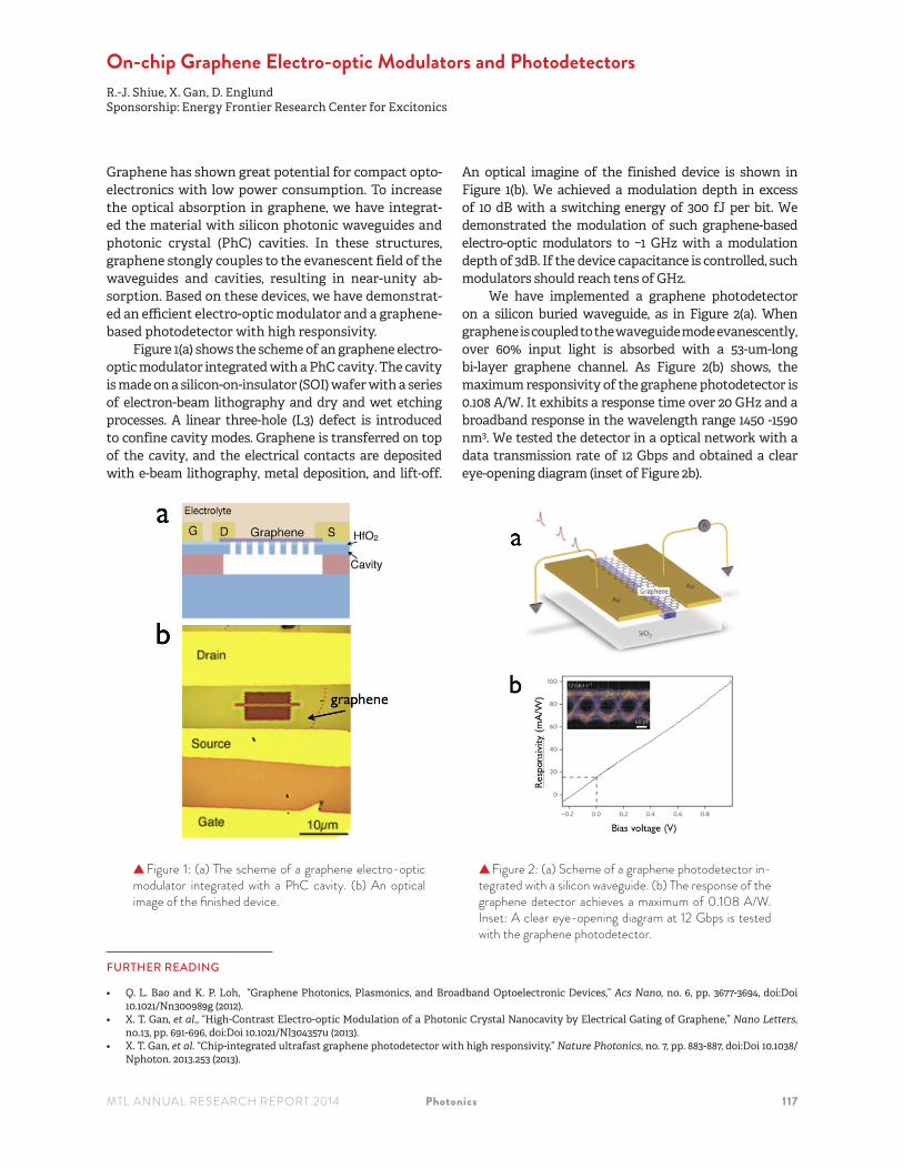
Figure 1(a) shows the scheme of an graphene electro-optic modulator integrated with a PhC cavity. The cavity is made on a silicon-on-insulator (SOI) wafer with a series of electron-beam lithography and dry and wet etching processes. A linear three-hole (L3) defect is introduced to confine cavity modes. Graphene is transferred on top of the cavity, and the electrical contacts are deposited with e-beam lithography, metal deposition, and lift-off.
An optical imagine of the finished device is shown in Figure 1(b). We achieved a modulation depth in excess of 10 dB with a switching energy of 300 fJ per bit. We demonstrated the modulation of such graphene-based electro-optic modulators to ~1 GHz with a modulation depth of 3dB. If the device capacitance is controlled, such modulators should reach tens of GHz.
We have implemented a graphene photodetector on a silicon buried waveguide, as in Figure 2(a). When graphene is coupled to the waveguide mode evanescently, over 60% input light is absorbed with a 53-um-long bi-layer graphene channel. As Figure 2(b) shows, the maximum responsivity of the graphene photodetector is 0.108 A/W. It exhibits a response time over 20 GHz and a broadband response in the wavelength range 1450 -1590 nm3. We tested the detector in a optical network with a data transmission rate of 12 Gbps and obtained a clear eye-opening diagram (inset of Figure 2b).
▲Figure 1: (a) The scheme of a graphene electro-optic modulator integrated with a PhC cavity. (b) An optical image of the finished device.
▲Figure 2: (a) Scheme of a graphene photodetector in-tegrated with a silicon waveguide. (b) The response of the graphene detector achieves a maximum of 0.108 A/W. Inset: A clear eye-opening diagram at 12 Gbps is tested with the graphene photodetector.
FURTHER READING
• Q. L. Bao and K. P. Loh, “Graphene Photonics, Plasmonics, and Broadband Optoelectronic Devices,” Acs Nano, no. 6, pp. 3677-3694, doi:Doi 10.1021/Nn300989g (2012).
• X. T. Gan, et al., “High-Contrast Electro-optic Modulation of a Photonic Crystal Nanocavity by Electrical Gating of Graphene,” Nano Letters, no.13, pp. 691-696, doi:Doi 10.1021/Nl304357u (2013).
• X. T. Gan, et al. “Chip-integrated ultrafast graphene photodetector with high responsivity,” Nature Photonics, no. 7, pp. 883-887, doi:Doi 10.1038/Nphoton. 2013.253 (2013).
118 Photonics MTL ANNUAL RESEARCH REPORT 2014
Graphene Mid-IR PhotodetectorsP.K. Herring, A.L. Hsu, N.M. Gabor, Y.C. Shin, J. Kong, T. Palacios, P. Jarillo-Herrero Sponsorship: Air Force Office of Scientific Research
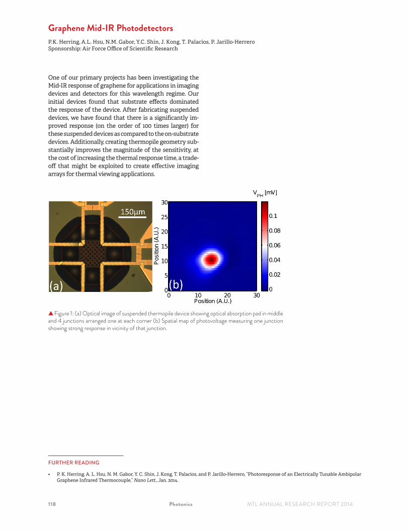
One of our primary projects has been investigating the Mid-IR response of graphene for applications in imaging devices and detectors for this wavelength regime. Our initial devices found that substrate effects dominated the response of the device. After fabricating suspended devices, we have found that there is a significantly im-proved response (on the order of 100 times larger) for these suspended devices as compared to the on-substrate devices. Additionally, creating thermopile geometry sub-stantially improves the magnitude of the sensitivity, at the cost of increasing the thermal response time, a trade-off that might be exploited to create effective imaging arrays for thermal viewing applications.
▲Figure 1: (a) Optical image of suspended thermopile device showing optical absorption pad in middle and 4 junctions arranged one at each corner (b) Spatial map of photovoltage measuring one junction showing strong response in vicinity of that junction.
FURTHER READING
• P. K. Herring, A. L. Hsu, N. M. Gabor, Y. C. Shin, J. Kong, T. Palacios, and P. Jarillo-Herrero, “Photoresponse of an Electrically Tunable Ambipolar Graphene Infrared Thermocouple,” Nano Lett., Jan. 2014.
MTL ANNUAL RESEARCH REPORT 2014 Photonics 119
Optoelectronics Based on Monolayer WSe2 p-n DiodesB. Baugher, H. Churchill, Y. Yang, P. Jarillo-Herrero Sponsorship: Office of Naval Research
The p–n junction is the functional element of many electronic and optoelectronic devices, including diodes, bipolar transistors, photodetectors, light-emitting di-odes, and solar cells. In conventional p–n junctions, the adjacent p- and n-type regions of a semiconductor are formed by chemical doping. Ambipolar semiconduc-tors, such as carbon nanotubes, nano-wires, and organ-ic molecules, allow p–n junctions to be configured and modified by electrostatic gating. This electrical control enables a single device to have multiple functionalities.
Through this initiative, we have pioneered a new class of electrostatically controlled ambipolar p-n junctions, utilizing monolayer WSe2. With these electrically tunable p–n junctions, we have demonstrated both p–n and n–p diodes with ideality
factors better than 2. Under optical excitation, the diodes demonstrate a photodetection responsivity of 210 mAW–1 and photovoltaic power generation with a peak external quantum efficiency of 0.2%, promising values for a nearly transparent monolayer material in a lateral device geometry. Finally, we have demonstrated a light-emitting diode based on monolayer WSe2.
These p–n diodes demonstrate the potential of monolayer WSe2, in addition to other direct-gap semiconducting dichalcogenides, for novel electronic and optoelectronic applications. Such devices may provide the building blocks for ultrathin, flexible, and nearly transparent optoelectronic and electronic devices. As quality improves, they also lay the foundation for more fundamental quantum transport experiments.
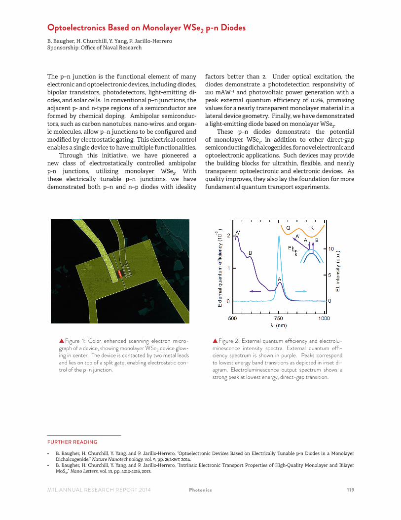
▲Figure 1: Color enhanced scanning electron micro-graph of a device, showing monolayer WSe2 device glow-ing in center. The device is contacted by two metal leads and lies on top of a split gate, enabling electrostatic con-trol of the p-n junction.
▲Figure 2: External quantum efficiency and electrolu-minescence intensity spectra. External quantum effi-ciency spectrum is shown in purple. Peaks correspond to lowest energy band transitions as depicted in inset di-agram. Electroluminescence output spectrum shows a strong peak at lowest energy, direct-gap transition.
FURTHER READING
• B. Baugher, H. Churchill, Y. Yang, and P. Jarillo-Herrero, “Optoelectronic Devices Based on Electrically Tunable p-n Diodes in a Monolayer Dichalcogenide,” Nature Nanotechnology, vol. 9, pp. 262-267, 2014.
• B. Baugher, H. Churchill, Y. Yang, and P. Jarillo-Herrero, “Intrinsic Electronic Transport Properties of High-Quality Monolayer and Bilayer MoS2,” Nano Letters, vol. 13, pp. 4212-4216, 2013.
120 Photonics MTL ANNUAL RESEARCH REPORT 2014
Bio-inspired and Bio-manufactured Photonic MaterialsM. KolleSponsorship: Alexander von Humboldt Foundation, Air Force Office of Scientific Research
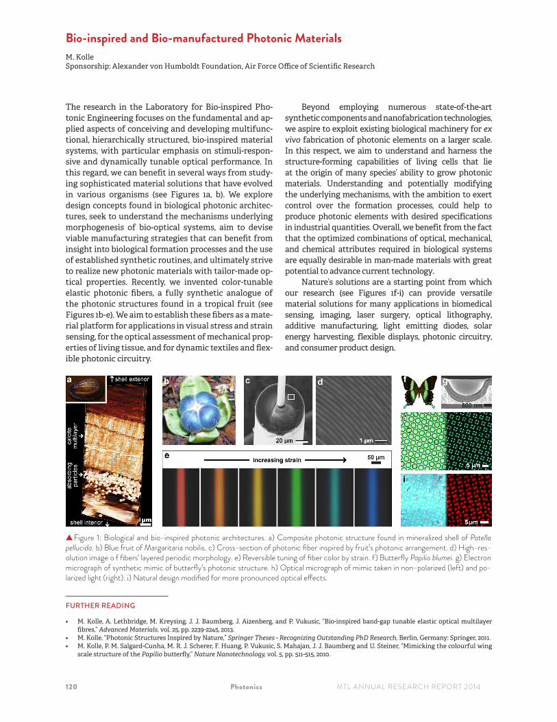
The research in the Laboratory for Bio-inspired Pho-tonic Engineering focuses on the fundamental and ap-plied aspects of conceiving and developing multifunc-tional, hierarchically structured, bio-inspired material systems, with particular emphasis on stimuli-respon-sive and dynamically tunable optical performance. In this regard, we can benefit in several ways from study-ing sophisticated material solutions that have evolved in various organisms (see Figures 1a, b). We explore design concepts found in biological photonic architec-tures, seek to understand the mechanisms underlying morphogenesis of bio-optical systems, aim to devise viable manufacturing strategies that can benefit from insight into biological formation processes and the use of established synthetic routines, and ultimately strive to realize new photonic materials with tailor-made op-tical properties. Recently, we invented color-tunable elastic photonic fibers, a fully synthetic analogue of the photonic structures found in a tropical fruit (see Figures 1b-e). We aim to establish these fibers as a mate-rial platform for applications in visual stress and strain sensing, for the optical assessment of mechanical prop-erties of living tissue, and for dynamic textiles and flex-ible photonic circuitry.
Beyond employing numerous state-of-the-art synthetic components and nanofabrication technologies, we aspire to exploit existing biological machinery for ex vivo fabrication of photonic elements on a larger scale. In this respect, we aim to understand and harness the structure-forming capabilities of living cells that lie at the origin of many species’ ability to grow photonic materials. Understanding and potentially modifying the underlying mechanisms, with the ambition to exert control over the formation processes, could help to produce photonic elements with desired specifications in industrial quantities. Overall, we benefit from the fact that the optimized combinations of optical, mechanical, and chemical attributes required in biological systems are equally desirable in man-made materials with great potential to advance current technology.
Nature’s solutions are a starting point from which our research (see Figures 1f-i) can provide versatile material solutions for many applications in biomedical sensing, imaging, laser surgery, optical lithography, additive manufacturing, light emitting diodes, solar energy harvesting, flexible displays, photonic circuitry, and consumer product design.
▲Figure 1: Biological and bio-inspired photonic architectures. a) Composite photonic structure found in mineralized shell of Patella pellucida. b) Blue fruit of Margaritaria nobilis. c) Cross-section of photonic fiber inspired by fruit’s photonic arrangement. d) High-res-olution image o f fibers’ layered periodic morphology. e) Reversible tuning of fiber color by strain. f) Butterfly Papilio blumei. g) Electron micrograph of synthetic mimic of butterfly’s photonic structure. h) Optical micrograph of mimic taken in non-polarized (left) and po-larized light (right). i) Natural design modified for more pronounced optical effects.
FURTHER READING
• M. Kolle, A. Lethbridge, M. Kreysing, J. J. Baumberg, J. Aizenberg, and P. Vukusic, “Bio-inspired band-gap tunable elastic optical multilayer fibres,” Advanced Materials, vol. 25, pp. 2239-2245, 2013.
• M. Kolle, “Photonic Structures Inspired by Nature,” Springer Theses - Recognizing Outstanding PhD Research, Berlin, Germany: Springer, 2011.• M. Kolle, P. M. Salgard-Cunha, M. R. J. Scherer, F. Huang, P. Vukusic, S. Mahajan, J. J. Baumberg and U. Steiner, “Mimicking the colourful wing
scale structure of the Papilio butterfly,” Nature Nanotechnology, vol. 5, pp. 511-515, 2010.