85
Photovoltaic and Photoelectrochemical Solar Cells Dr. Katarzyna Skorupska
Photovoltaic and Photoelectrochemical Solar Cells
Dr. Katarzyna Skorupska
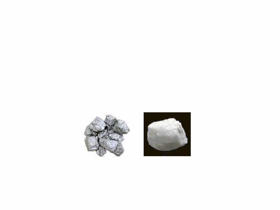
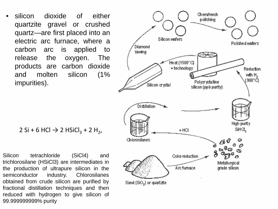
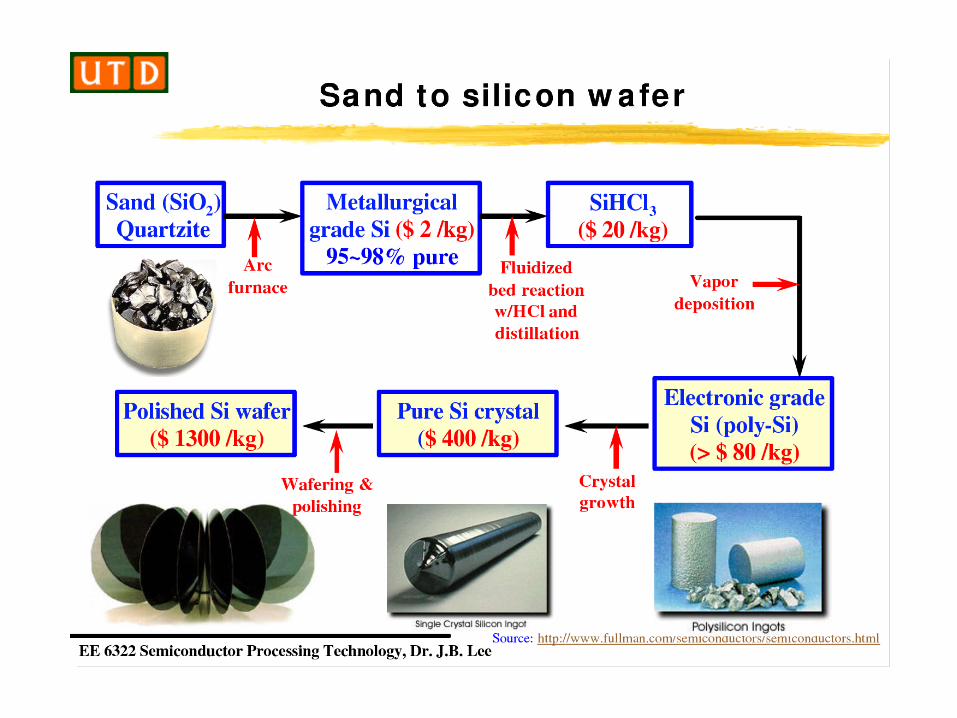
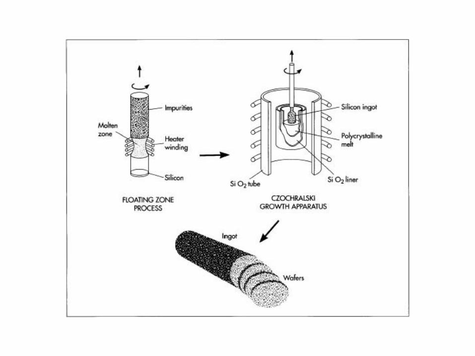
• silicon dioxide of either quartzite gravel or crushed quartz—are first placed into an electric arc furnace, where a carbon arc is applied to release the oxygen. The products are carbon dioxide and molten silicon (1% impurities).
2 Si + 6 HCl → 2 HSiCl3 + 2 H2,
Silicon tetrachloride (SiCl4) and trichlorosilane (HSiCl3) are intermediates in the production of ultrapure silicon in the semiconductor industry. Chlorosilanes obtained from crude silicon are purified by fractional distillation techniques and then reduced with hydrogen to give silicon of 99.999999999% purity

Prof. Jan Czochralski
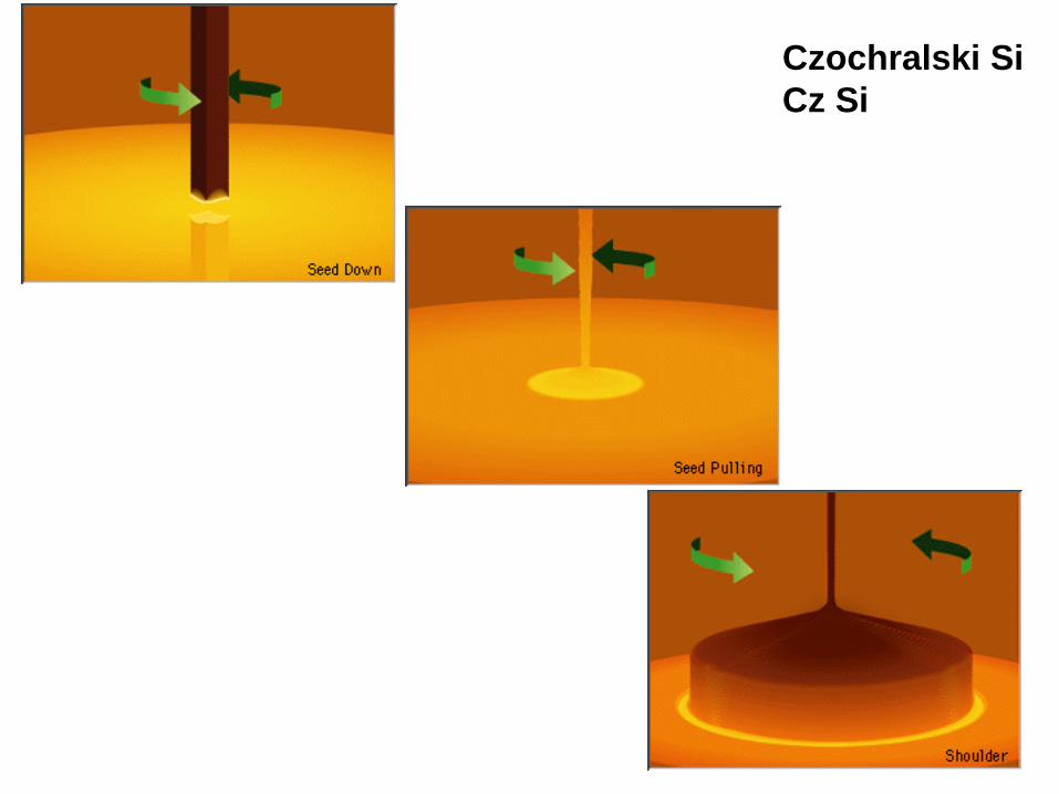
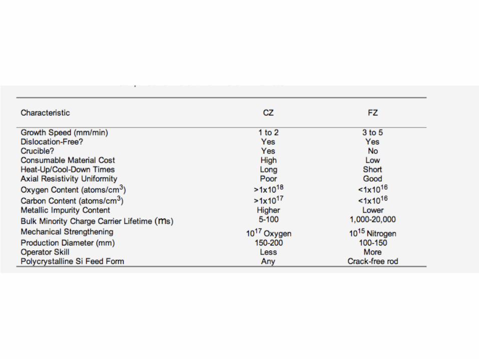
Czochralski Si Cz Si
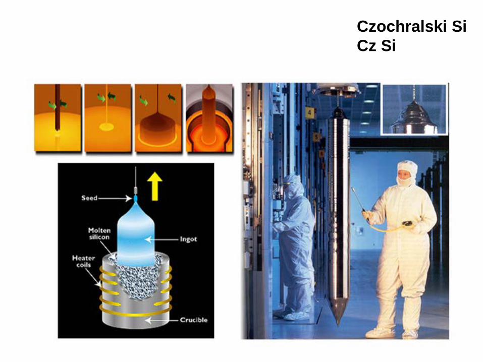
Czochralski Si Cz Si
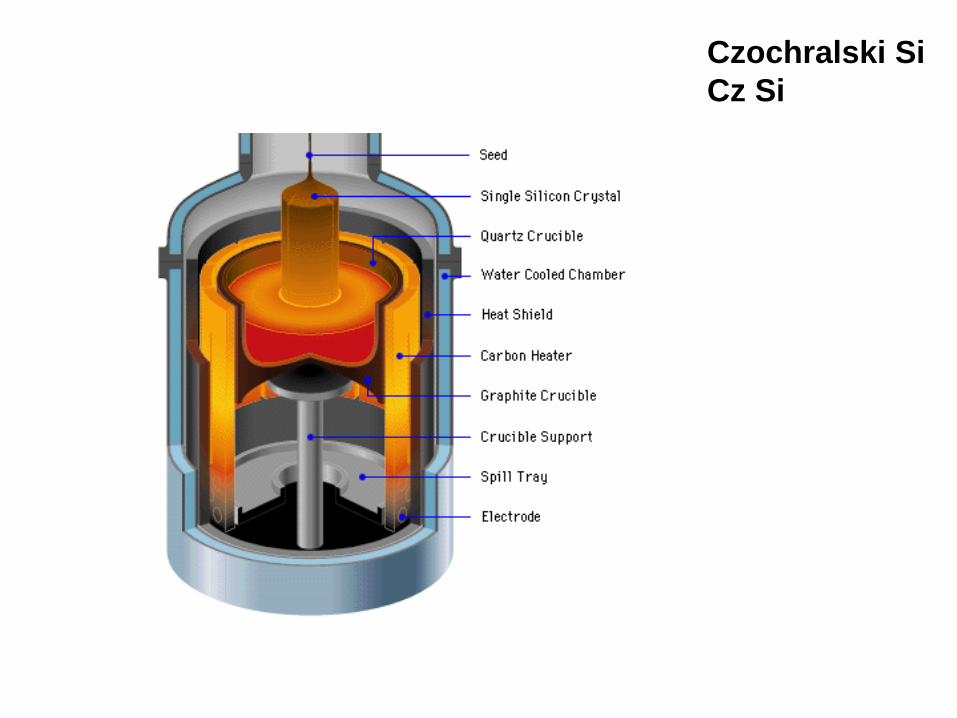
Czochralski Si Cz Si
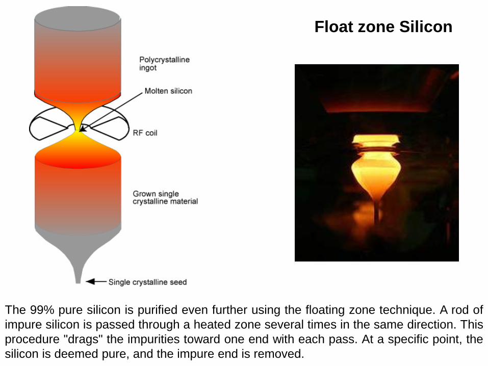
The 99% pure silicon is purified even further using the floating zone technique. A rod of impure silicon is passed through a heated zone several times in the same direction. This procedure "drags" the impurities toward one end with each pass. At a specific point, the silicon is deemed pure, and the impure end is removed.
Float zone Silicon
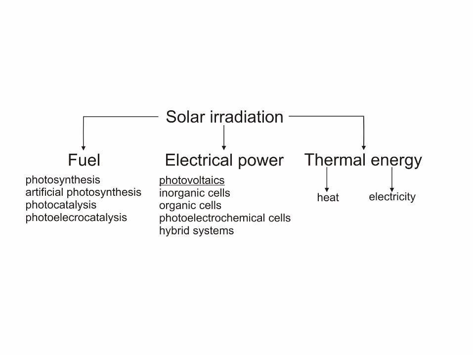
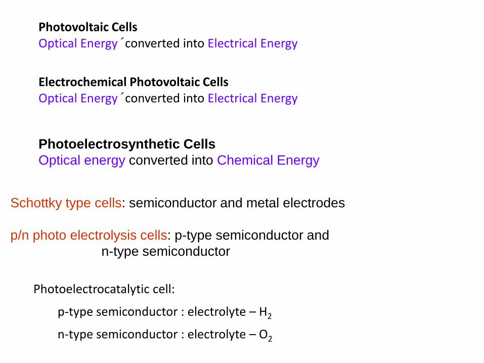
Electrochemical Photovoltaic Cells Optical Energy ´converted into Electrical Energy
Photoelectrocatalytic cell:
p-type semiconductor : electrolyte – H2
n-type semiconductor : electrolyte – O2
Photoelectrosynthetic Cells Optical energy converted into Chemical Energy
Schottky type cells: semiconductor and metal electrodes p/n photo electrolysis cells: p-type semiconductor and n-type semiconductor
Photovoltaic Cells Optical Energy ´converted into Electrical Energy
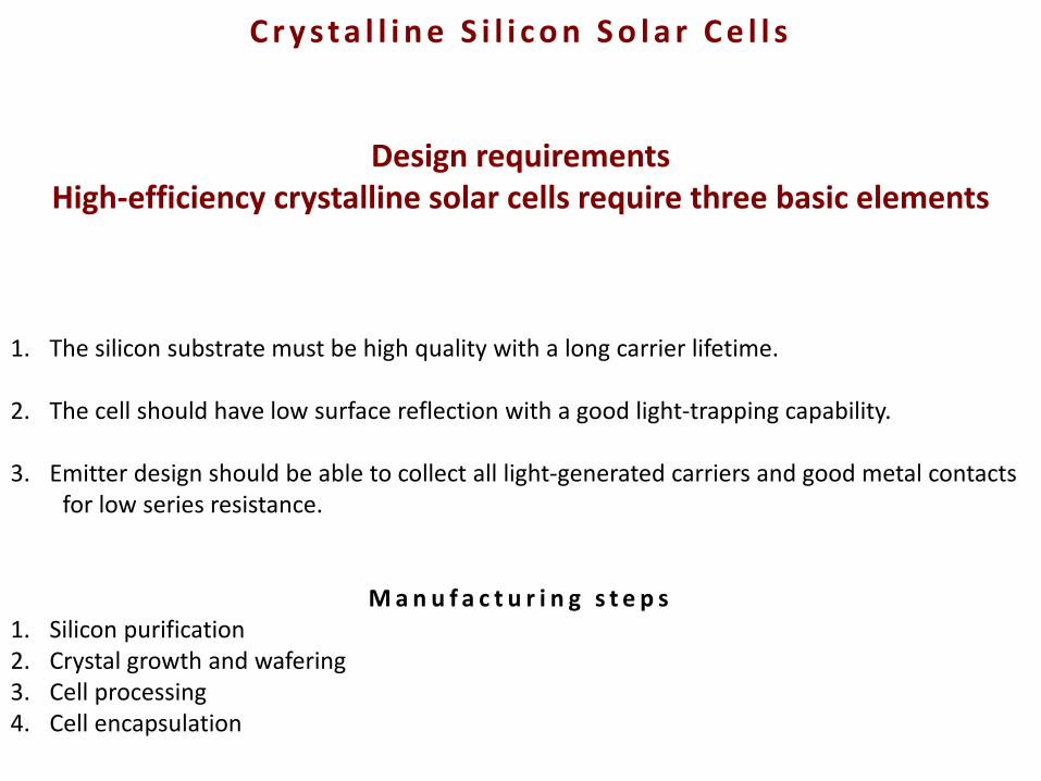
Design requirements High-efficiency crystalline solar cells require three basic elements
1. The silicon substrate must be high quality with a long carrier lifetime.
2. The cell should have low surface reflection with a good light-trapping capability.
3. Emitter design should be able to collect all light-generated carriers and good metal contacts
for low series resistance.
M a n u f a c t u r i n g s t e p s
1. Silicon purification 2. Crystal growth and wafering 3. Cell processing 4. Cell encapsulation
C r y s ta l l i n e S i l i c o n S o l a r C e l l s
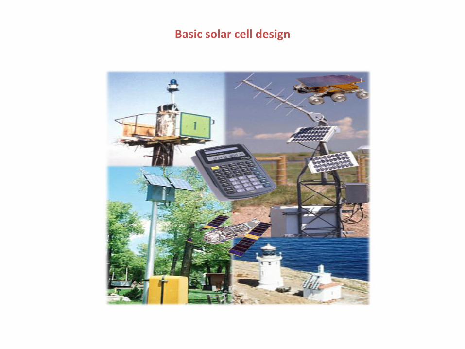
Basic solar cell design
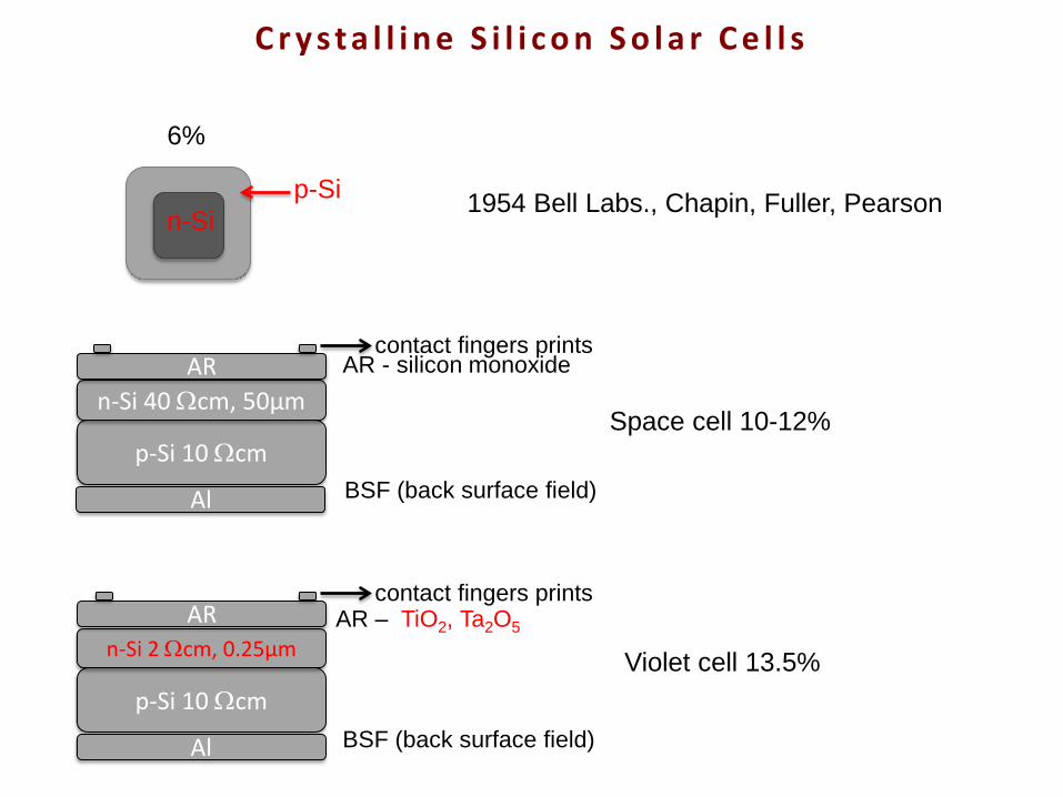
C r y s ta l l i n e S i l i c o n S o l a r C e l l s
1954 Bell Labs., Chapin, Fuller, Pearson n-Si
p-Si
6%
Space cell 10-12%
Violet cell 13.5%
p-Si 10 Ωcm
n-Si 40 Ωcm, 50µm AR
Al BSF (back surface field)
AR - silicon monoxide contact fingers prints
AR – TiO2, Ta2O5
p-Si 10 Ωcm
n-Si 2 Ωcm, 0.25µm AR
Al
contact fingers prints
BSF (back surface field)
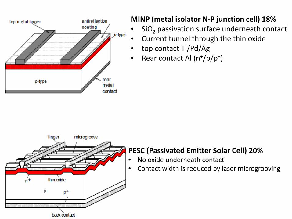
MINP (metal isolator N-P junction cell) 18% • SiO2 passivation surface underneath contact • Current tunnel through the thin oxide • top contact Ti/Pd/Ag • Rear contact Al (n+/p/p+)
PESC (Passivated Emitter Solar Cell) 20% • No oxide underneath contact • Contact width is reduced by laser microgrooving
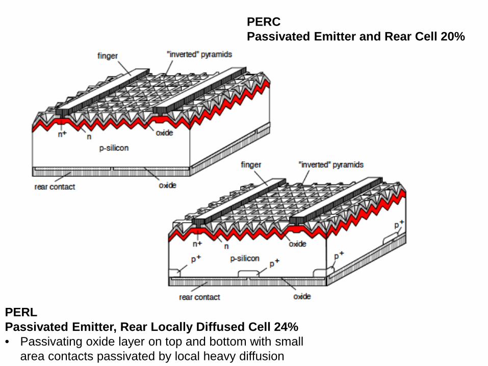
PERC Passivated Emitter and Rear Cell 20%
PERL Passivated Emitter, Rear Locally Diffused Cell 24% • Passivating oxide layer on top and bottom with small
area contacts passivated by local heavy diffusion
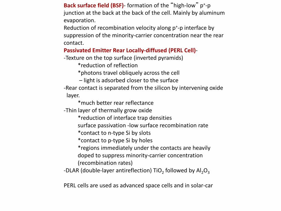
Back surface field (BSF)- formation of the “high-low” p+-p junction at the back at the back of the cell. Mainly by aluminum evaporation. Reduction of recombination velocity along p+-p interface by suppression of the minority-carrier concentration near the rear contact. Passivated Emitter Rear Locally-diffused (PERL Cell)- -Texture on the top surface (inverted pyramids) *reduction of reflection *photons travel obliquely across the cell – light is adsorbed closer to the surface -Rear contact is separated from the silicon by intervening oxide layer. *much better rear reflectance -Thin layer of thermally grow oxide *reduction of interface trap densities surface passivation -low surface recombination rate *contact to n-type Si by slots *contact to p-type Si by holes *regions immediately under the contacts are heavily doped to suppress minority-carrier concentration (recombination rates) -DLAR (double-layer antireflection) TiO2 followed by Al2O3 PERL cells are used as advanced space cells and in solar-car

Spectral improvement
µmmcmx
x
cmfor
µmmcmx
cmfor
µmmmcmx
cmfor
xforeI
I
eII
eII
x
x
1.00000001.000001.0101110
1000001.0001.01011
10
100001.0101.01.01011
10
11
5
153
3
132
21
111
0
0
0
=====
=
=====
=
==•====
=
==
=
=
−
−
−
−
−
−
αα
αα
α
α
α
α
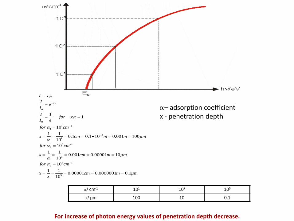
α– adsorption coefficient x - penetration depth
α/ cm-1 101 103 105
x/ µm 100 10 0.1
For increase of photon energy values of penetration depth decrease.
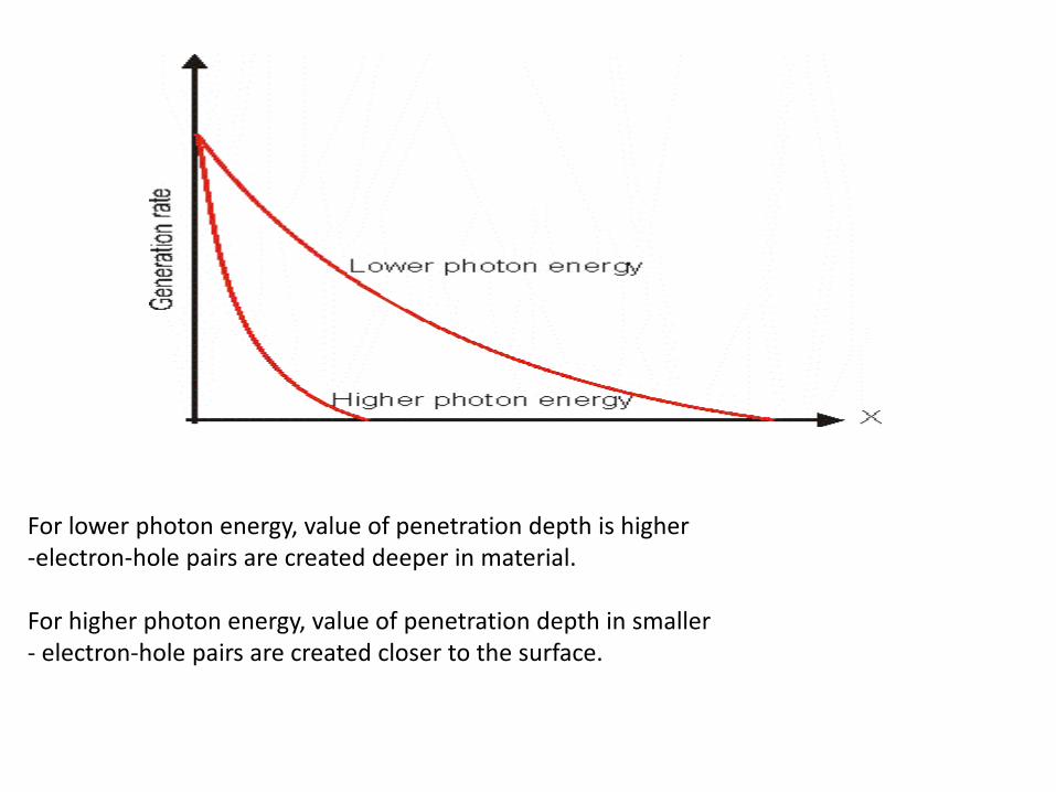
For lower photon energy, value of penetration depth is higher -electron-hole pairs are created deeper in material.
For higher photon energy, value of penetration depth in smaller - electron-hole pairs are created closer to the surface.
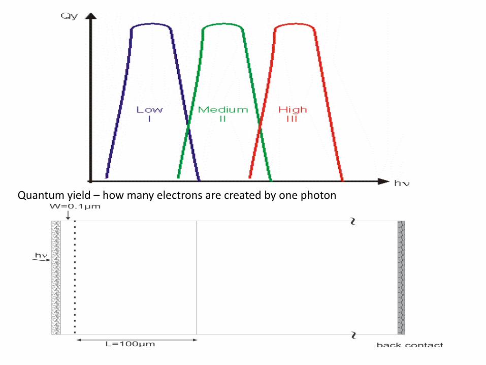
Quantum yield – how many electrons are created by one photon
Spectral behaviour cont´d
Consider schematical spectral response: what are the spatial contributions to the light-induced current jL
Spatial contributions: xα large: carriers from neutral region of device (1) xα medium range: carriers from neutral region and space charge layer (2) xα small: carriers from surface-near region (n+-layer) (3)
Spectral response- number of carriers collected per incident photon at each wave length. deal internal spectral response for a semiconductor with energy gap Eg: for hν<Eg equals 0 and for hν>Eg equals unity At low photon energies, most carriers are generated in the base region because of the low coefficient in Si. As photon energy increases above 2.5eV, the front region takes over. Above 3.5eV, α becomes lager than 106 cm-1, and the spectral response derives entirely from front region.
Departure from the ideal response - recombination of carriers To increase the spectral response: - increase the diffusion length - decrease recombination velocity for electrons and holes
Back surface field
The n+ - p - p+ junction before contact: (exercise-draw the junction after contact formation.
The construction of E(x) begins with the already formed n+-p junction p+
EF
Spectral improvement cont´d
The Fermi level of the (highest doped) n+ part dominates; after contact formation, its energetic position defines mostly EF
C:
The BSF reduces the back surface recombination velocity to ~10cm/s
The reflectivity of Si for normal incidence is 34% at 1100 nm (1.12 eV) and rises to 54% at 400 nm. Proper single layer AR coatings can reduce R ~ 10% in this wavelength range. With the pyramidal NR coating, reflectivity drops to ~ 3%
Advantages: • reflectivity drops • more effective absorption due to inclined light paths in Si • more charge carriers generated in depletion region • long wavelength light is absorbed more efficiently
pyramidal texturing The anisotropy of silicon etching with crystal orientation: surface atomic arrangement and :
top view of (111) and (001) surfaces
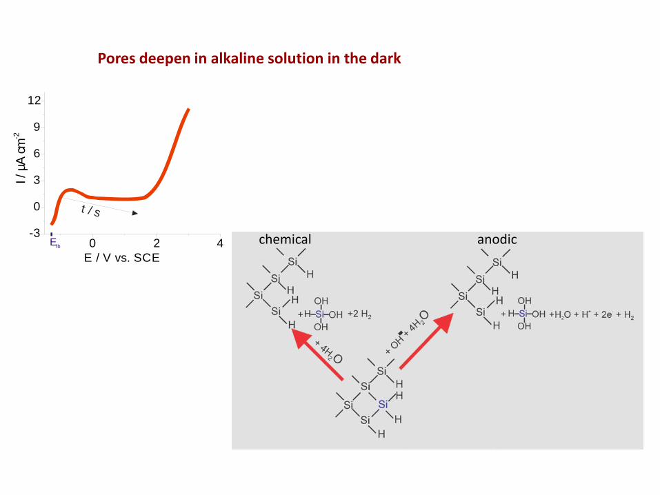
The etching procedure: Chemical etching of Si in alkaline solution (NaOH, KOH) Sis (=Si-H-H) + 2H2O H2Si(OH)2 (+2H attached to underlying latticeatoms) H2Si(OH)2 + 2H2O Si(OH)4 + 2H2 Etching is anisotropic with crystal orientation
Terrace dissolution
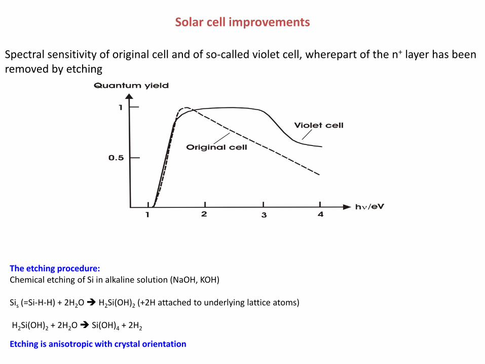
Solar cell improvements
Spectral sensitivity of original cell and of so-called violet cell, wherepart of the n+ layer has been removed by etching
The etching procedure: Chemical etching of Si in alkaline solution (NaOH, KOH) Sis (=Si-H-H) + 2H2O H2Si(OH)2 (+2H attached to underlying lattice atoms) H2Si(OH)2 + 2H2O Si(OH)4 + 2H2 Etching is anisotropic with crystal orientation
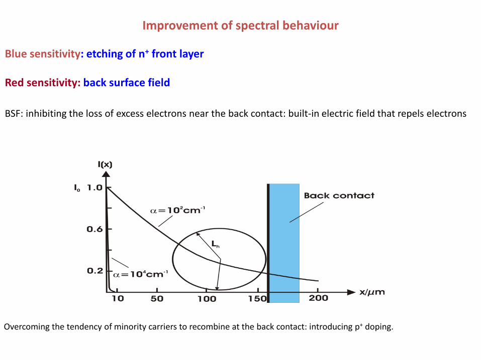
Improvement of spectral behaviour
Blue sensitivity: etching of n+ front layer Red sensitivity: back surface field
BSF: inhibiting the loss of excess electrons near the back contact: built-in electric field that repels electrons
Overcoming the tendency of minority carriers to recombine at the back contact: introducing p+ doping.
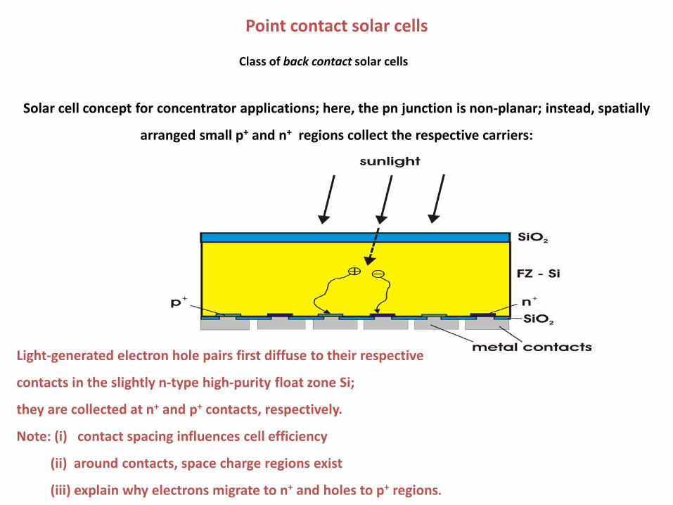
Point contact solar cells
Solar cell concept for concentrator applications; here, the pn junction is non-planar; instead, spatially
arranged small p+ and n+ regions collect the respective carriers:
Light-generated electron hole pairs first diffuse to their respective
contacts in the slightly n-type high-purity float zone Si;
they are collected at n+ and p+ contacts, respectively.
Note: (i) contact spacing influences cell efficiency
(ii) around contacts, space charge regions exist
(iii) explain why electrons migrate to n+ and holes to p+ regions.
Class of back contact solar cells
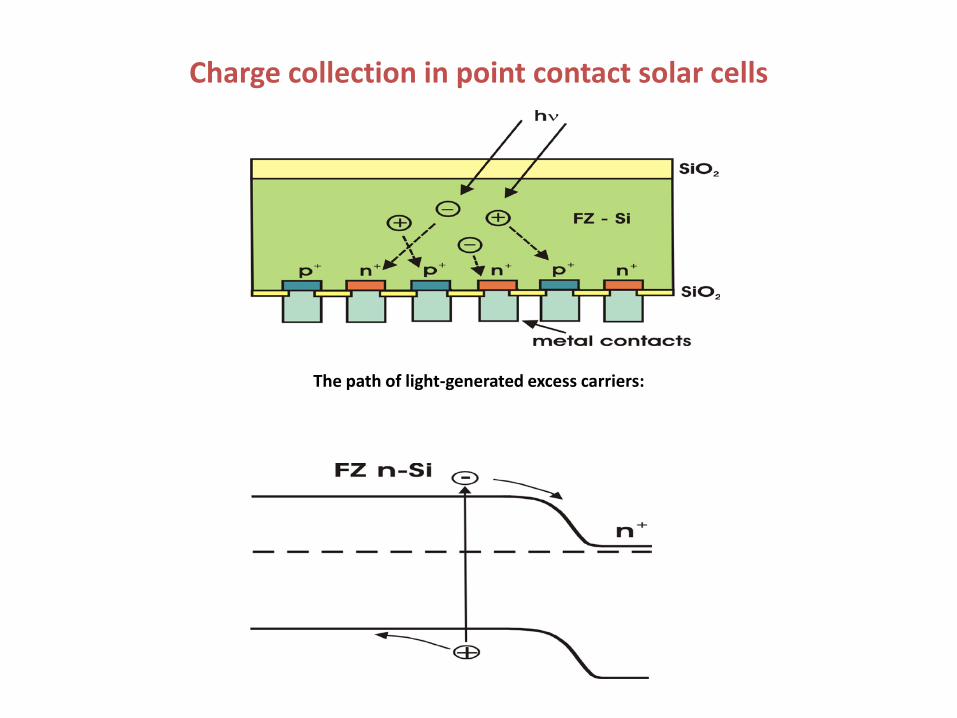
Charge collection in point contact solar cells
The path of light-generated excess carriers:


38
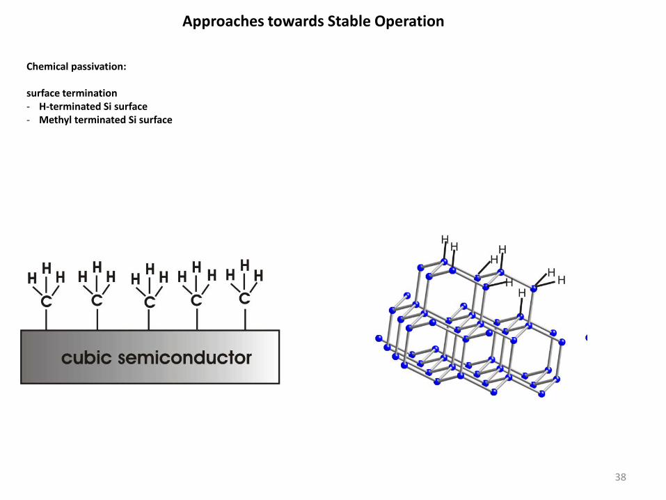
Chemical passivation: surface termination - H-terminated Si surface - Methyl terminated Si surface
Approaches towards Stable Operation
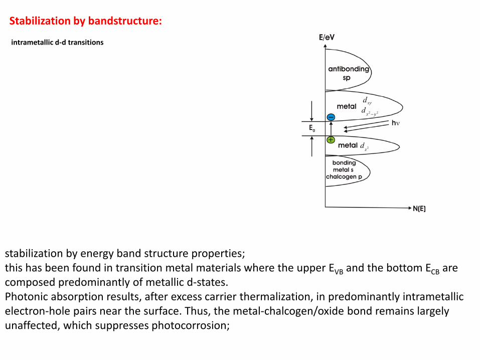
Stabilization by bandstructure: intrametallic d-d transitions
stabilization by energy band structure properties; this has been found in transition metal materials where the upper EVB and the bottom ECB are composed predominantly of metallic d-states. Photonic absorption results, after excess carrier thermalization, in predominantly intrametallic electron-hole pairs near the surface. Thus, the metal-chalcogen/oxide bond remains largely unaffected, which suppresses photocorrosion;
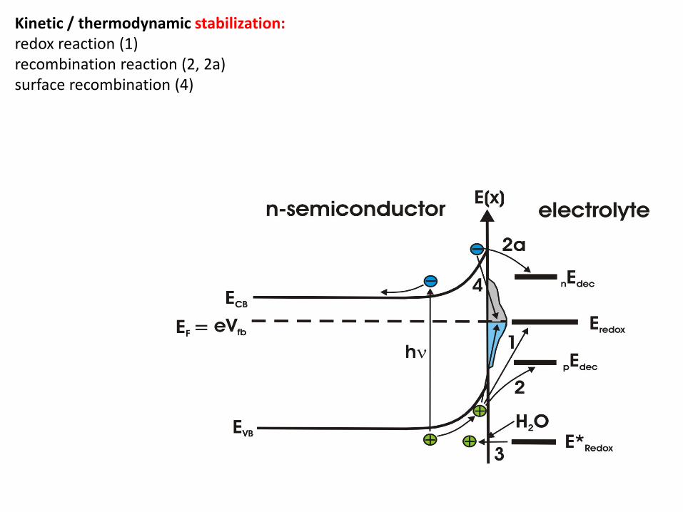
Kinetic / thermodynamic stabilization: redox reaction (1) recombination reaction (2, 2a) surface recombination (4)
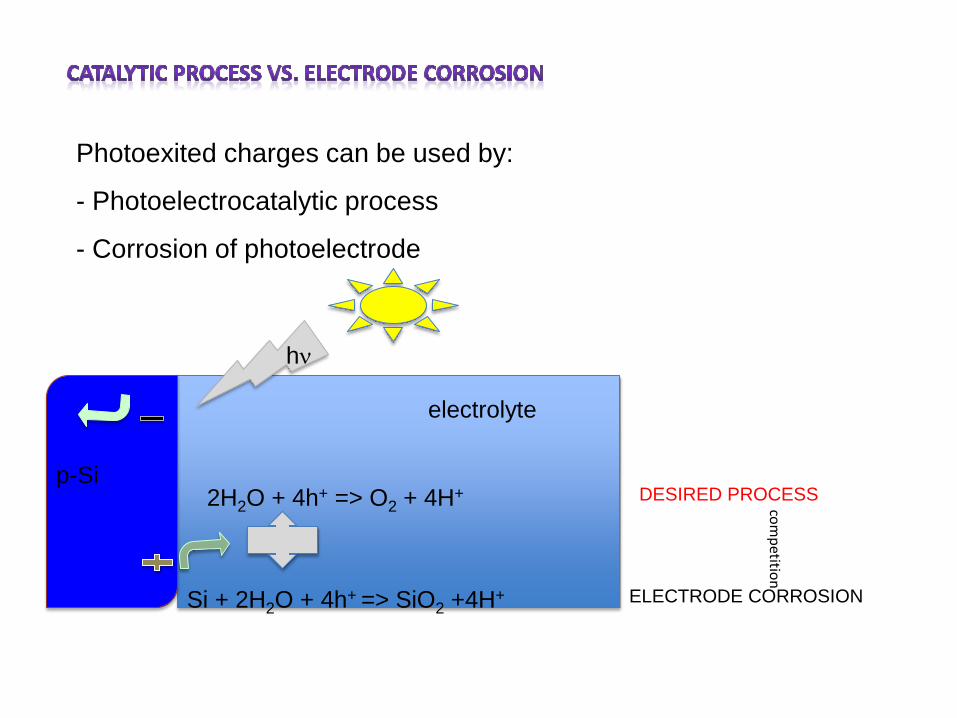
Photoexited charges can be used by:
- Photoelectrocatalytic process
- Corrosion of photoelectrode
Si + 2H2O + 4h+ => SiO2 +4H+ ELECTRODE CORROSION
2H2O + 4h+ => O2 + 4H+ DESIRED PROCESS p-Si
electrolyte
hν
competition
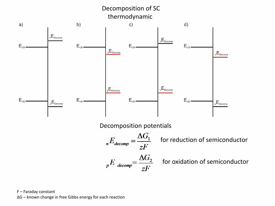
Decomposition of SC thermodynamic
F – Faraday constant ΔG – known change in free Gibbs energy for each reaction
Decomposition potentials
for reduction of semiconductor
for oxidation of semiconductor
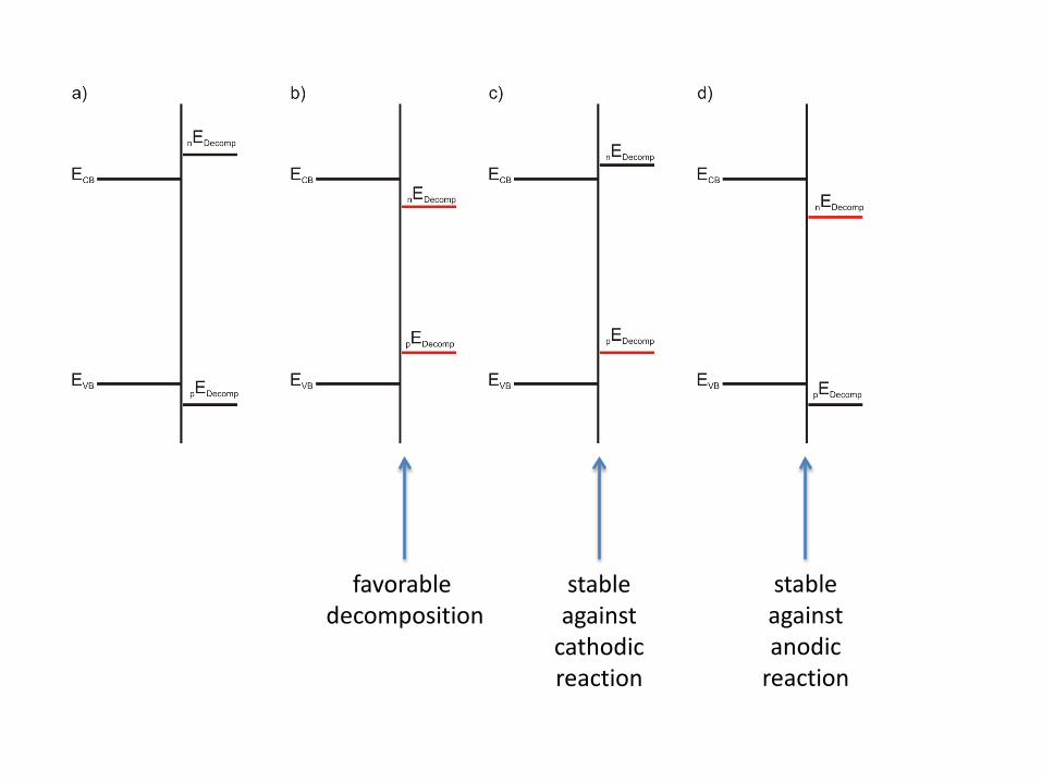
favorable decomposition
stable against
cathodic reaction
stable against anodic
reaction
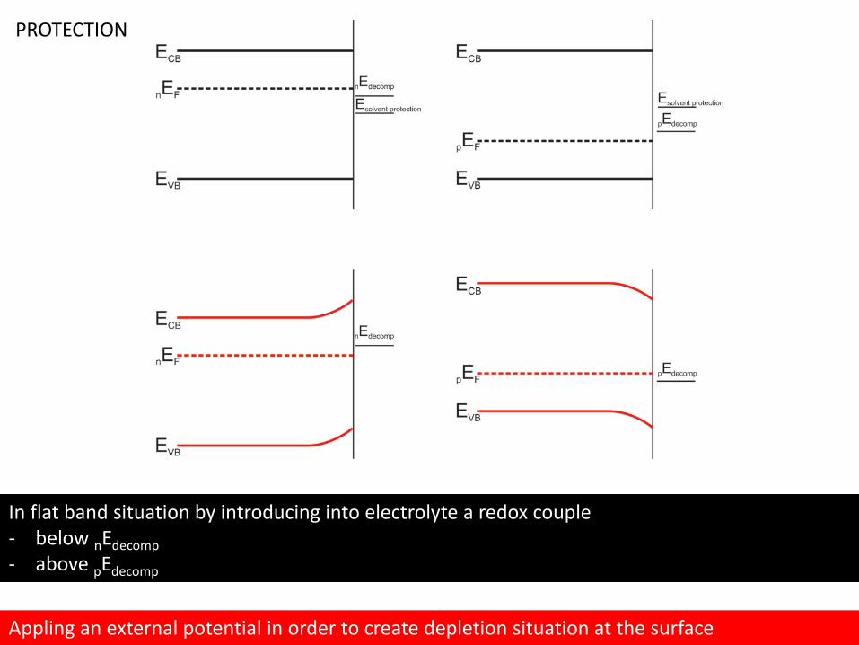
PROTECTION
In flat band situation by introducing into electrolyte a redox couple - below nEdecomp - above pEdecomp
Appling an external potential in order to create depletion situation at the surface
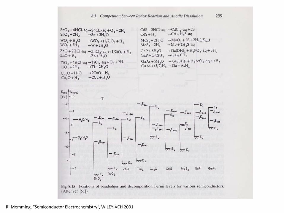
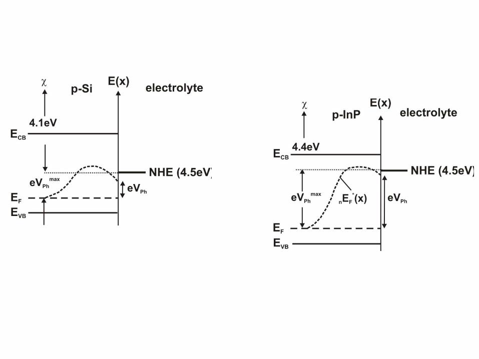
R. Memming, “Semiconductor Electrochemistry”, WILEY-VCH 2001
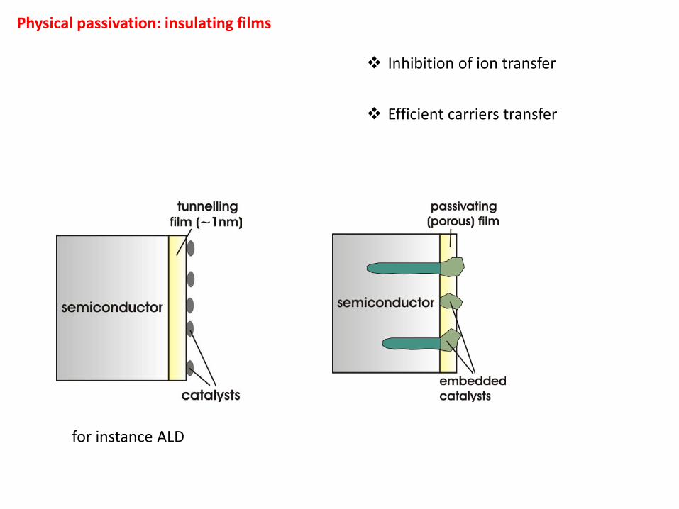
Physical passivation: insulating films
Inhibition of ion transfer
Efficient carriers transfer
for instance ALD
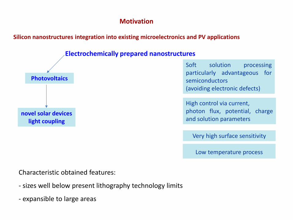
Motivation
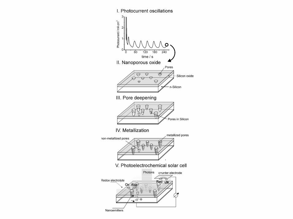
Silicon nanostructures integration into existing microelectronics and PV applications
Characteristic obtained features:
- sizes well below present lithography technology limits
- expansible to large areas
Electrochemically prepared nanostructures
Photovoltaics
novel solar devices light coupling
Soft solution processing particularly advantageous for semiconductors (avoiding electronic defects)
High control via current, photon flux, potential, charge and solution parameters
Very high surface sensitivity
Low temperature process
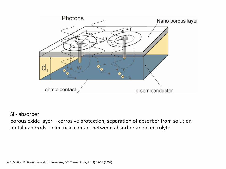
A.G. Muñoz, K. Skorupska and H.J. Lewerenz, ECS Transactions, 21 (1) 35-56 (2009)
Si - absorber porous oxide layer - corrosive protection, separation of absorber from solution metal nanorods – electrical contact between absorber and electrolyte
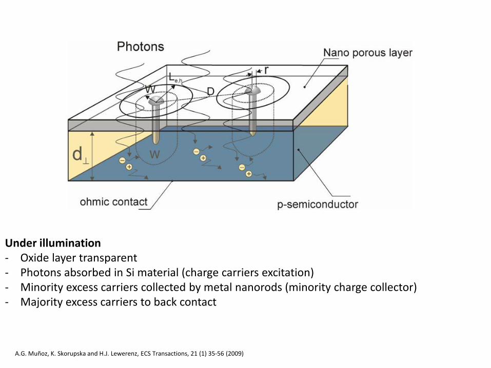
A.G. Muñoz, K. Skorupska and H.J. Lewerenz, ECS Transactions, 21 (1) 35-56 (2009)
Under illumination - Oxide layer transparent - Photons absorbed in Si material (charge carriers excitation) - Minority excess carriers collected by metal nanorods (minority charge collector) - Majority excess carriers to back contact
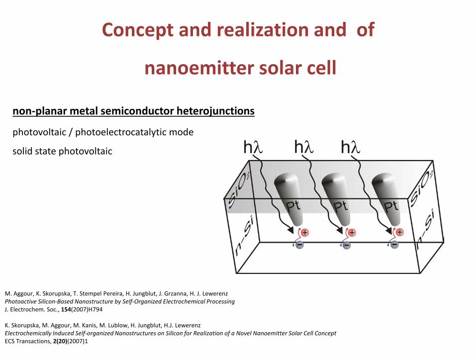
Concept and realization and of
nanoemitter solar cell
M. Aggour, K. Skorupska, T. Stempel Pereira, H. Jungblut, J. Grzanna, H. J. Lewerenz Photoactive Silicon-Based Nanostructure by Self-Organized Electrochemical Processing J. Electrochem. Soc., 154(2007)H794 K. Skorupska, M. Aggour, M. Kanis, M. Lublow, H. Jungblut, H.J. Lewerenz Electrochemically Induced Self-organized Nanostructures on Silicon for Realization of a Novel Nanoemitter Solar Cell Concept ECS Transactions, 2(20)(2007)1
photovoltaic / photoelectrocatalytic mode
solid state photovoltaic
non-planar metal semiconductor heterojunctions
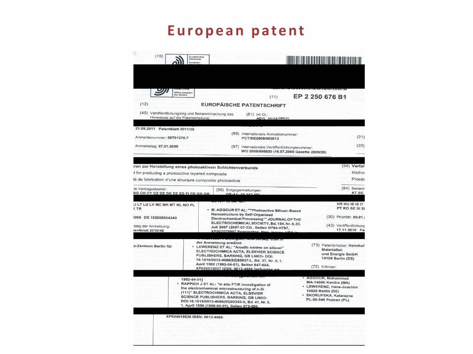
E u r o p e a n p a te nt
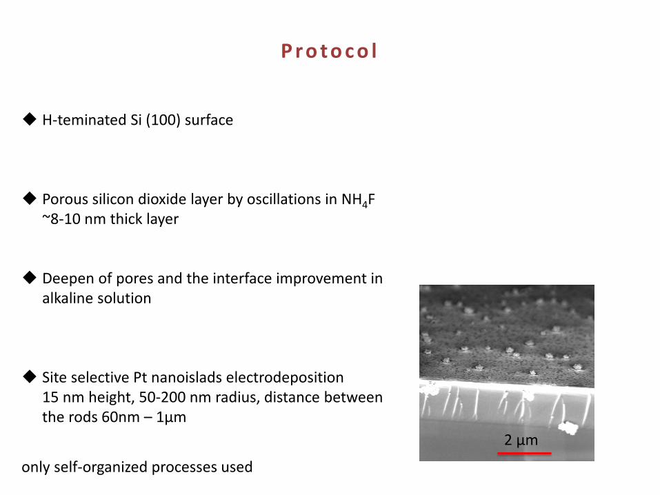
H-teminated Si (100) surface
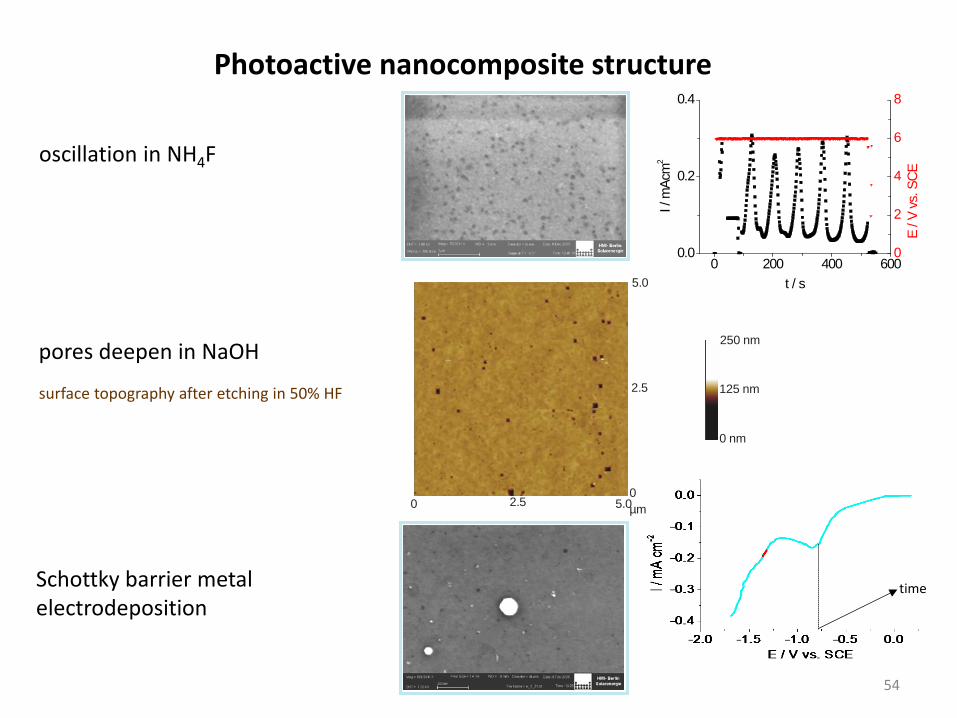
Porous silicon dioxide layer by oscillations in NH4F ~8-10 nm thick layer
Deepen of pores and the interface improvement in alkaline solution
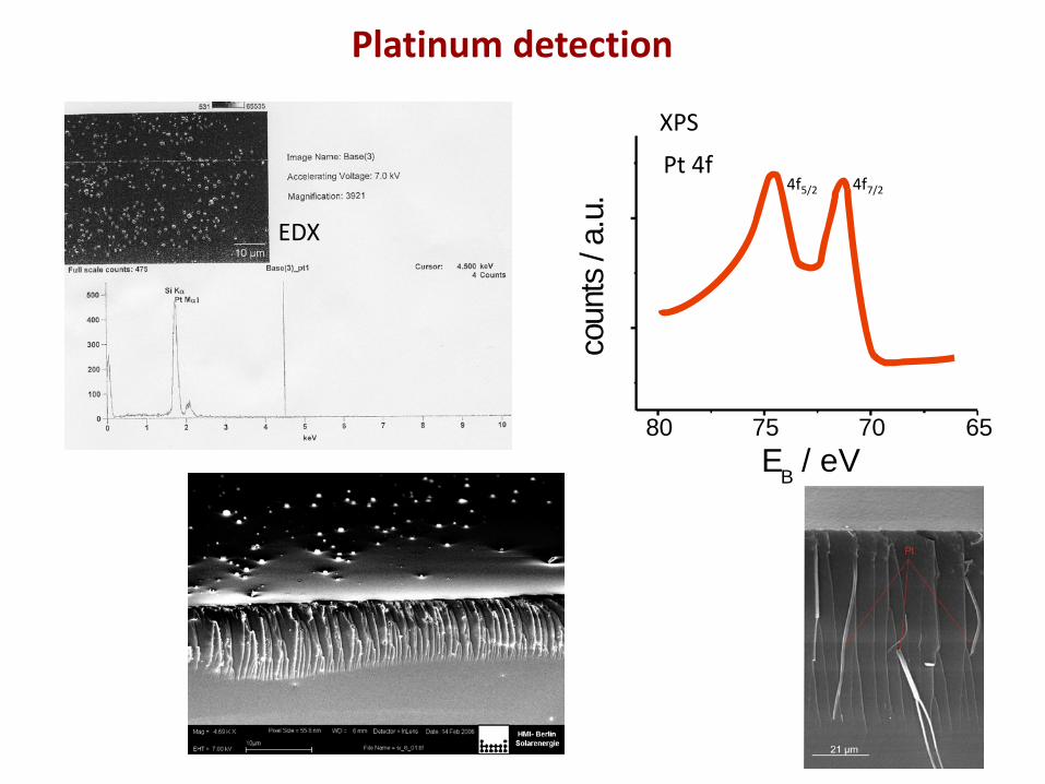
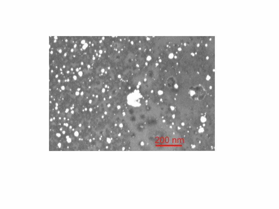
Site selective Pt nanoislads electrodeposition 15 nm height, 50-200 nm radius, distance between the rods 60nm – 1µm
2 µm
only self-organized processes used
P r o to c o l
54
Photoactive nanocomposite structure
oscillation in NH4F
pores deepen in NaOH
Schottky barrier metal electrodeposition
0 200 400 6000.0
0.2
0.4
0
2
4
6
8
E / V
vs.
SCE
I / m
Acm
2
t / s
time
surface topography after etching in 50% HF
0 2.5 5.0µm0
2.5
5.0
0 nm
125 nm
250 nm
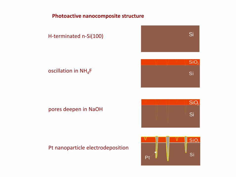
Photoactive nanocomposite structure
H-terminated n-Si(100)
oscillation in NH4F
pores deepen in NaOH
Pt nanoparticle electrodeposition
Si
SiO2
Si
SiO2
Si
SiO2
Pt
Si
Si
Si
SiO2
Si
SiO2
Si
SiO 2
Metal
0 200 400 600
0.0
0.5
1.0
phot
ocur
rent
/ m
Acm
-2
time / s
3 mA
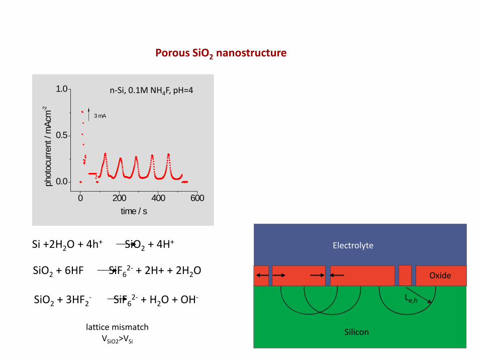
Si +2H2O + 4h+ SiO2 + 4H+
SiO2 + 6HF SiF62- + 2H+ + 2H2O
SiO2 + 3HF2- SiF6
2- + H2O + OH-
Electrolyte
Oxide
Le,h
Silicon
Porous SiO2 nanostructure
lattice mismatch VSiO2>VSi
n-Si, 0.1M NH4F, pH=4
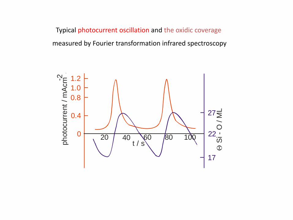
0
0.4
0.81.01.2
17
22
27
phot
ocur
rent
/ m
Acm
-
Θ S
i - O
/ M
L
- 2
20 40 60 80 100t / s
Typical photocurrent oscillation and the oxidic coverage
measured by Fourier transformation infrared spectroscopy
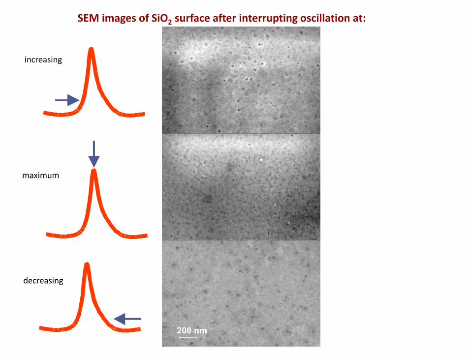
SEM images of SiO2 surface after interrupting oscillation at:
increasing
decreasing
maximum
Si
Si
SiO2
Si
SiO 2
Metal
Si
SiO2
0 2 4-3
0
3
6
9
12
I/µA
cm-2
E / V vs. SCE
t / s
Efbchemical anodic
Pores deepen in alkaline solution in the dark
34.17 nm61.60 nm
n-Si surface
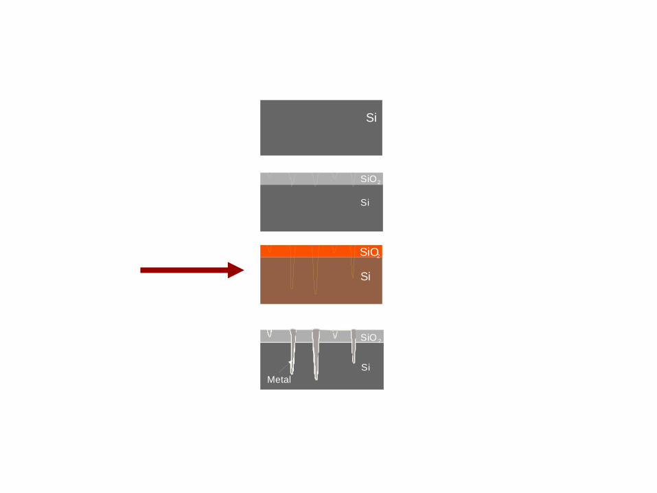
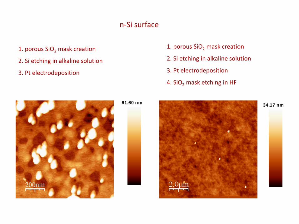
1. porous SiO2 mask creation
2. Si etching in alkaline solution
3. Pt electrodeposition
1. porous SiO2 mask creation
2. Si etching in alkaline solution
3. Pt electrodeposition
4. SiO2 mask etching in HF

Si
Si
SiO2
Si
SiO2
Si
SiO 2
Metal
200 nm 200 nm 200 nm
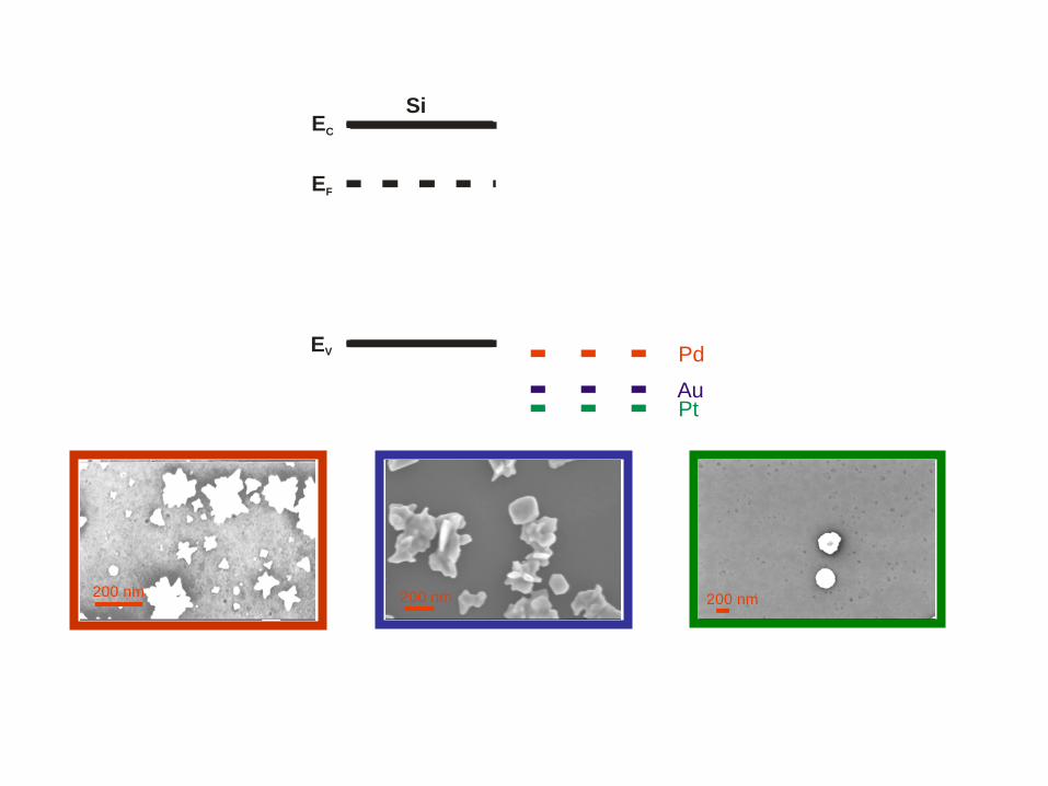
Pd
AuPt
SiEC
EF
EV
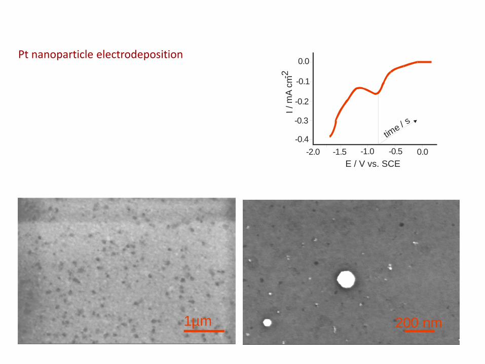
Pt nanoparticle electrodeposition
1µm 200 nm
E / V vs. SCE
0.0
-0.1
-0.2
-0.3
-0.4-2.0 -1.5 -1.0 -0.5 0.0
time / s
-2I /
mA
cm
80 75 70 65
coun
ts/a
.u.
EB / eV
Pt 4f 4f5/2 4f7/2
Platinum detection
XPS
EDX
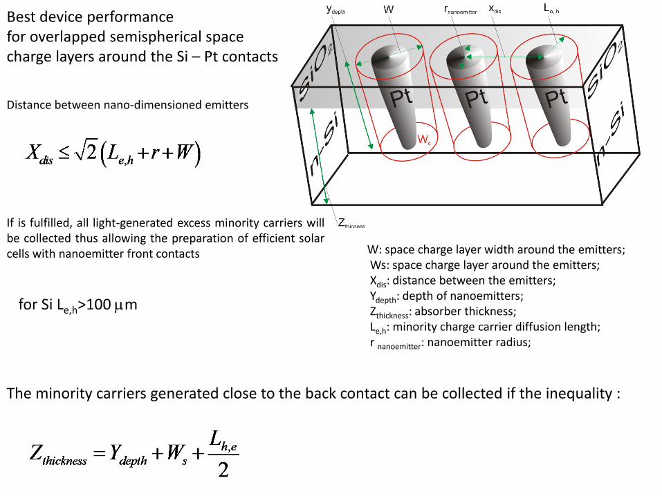
Best device performance for overlapped semispherical space charge layers around the Si – Pt contacts
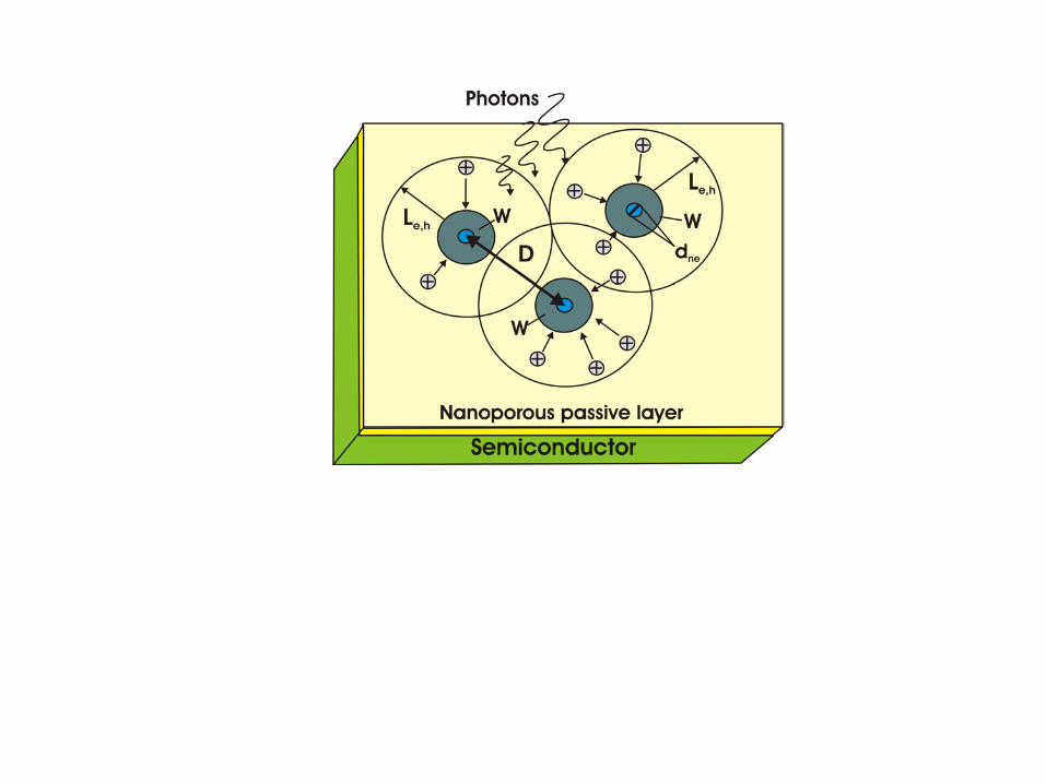
W: space charge layer width around the emitters; Ws: space charge layer around the emitters; Xdis: distance between the emitters; Ydepth: depth of nanoemitters; Zthickness: absorber thickness; Le,h: minority charge carrier diffusion length; r nanoemitter: nanoemitter radius;
Distance between nano-dimensioned emitters
If is fulfilled, all light-generated excess minority carriers will be collected thus allowing the preparation of efficient solar cells with nanoemitter front contacts
for Si Le,h>100 µm
The minority carriers generated close to the back contact can be collected if the inequality :
69
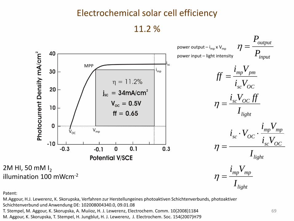
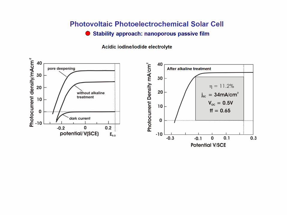
Electrochemical solar cell efficiency
11.2 %
2M HI, 50 mM I2 illumination 100 mWcm-2
Patent: M.Aggour, H.J. Lewerenz, K. Skorupska, Verfahren zur Herstellungeines photoaktiven Schichtenverbunds, photoaktiver Schichtenverbund und Anwendung DE: 102008004340.0, 09.01.08 T. Stempel, M. Aggour, K. Skorupska, A. Muiioz, H. J. Lewerenz, Electrochem. Comm. 10(2008)1184 M. Aggour, K. Skorupska, T. Stempel, H. Jungblut, H. J. Lewerenz, J. Electrochem. Soc. 154(2007)H79
input
output
PP
=ηpower output – imp x Vmp
power input – light intensity
OCsc
pmmp
ViVi
ff =
light
mpmp
light
OCsc
mpmpOCsc
light
OCsc
IVi
IViVi
Vi
IffVi
=
⋅⋅=
=
η
η
η
VOC Vmp
isc imp
MPP
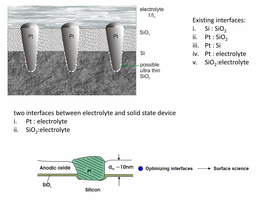
Existing interfaces: i. Si : SiO2 ii. Pt : SiO2 iii. Pt : Si iv. Pt : electrolyte v. SiO2:electrolyte
two interfaces between electrolyte and solid state device i. Pt : electrolyte ii. SiO2:electrolyte
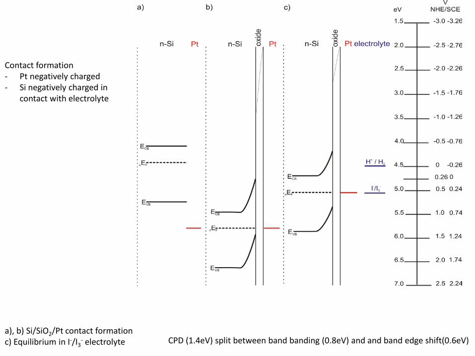
Contact formation - Pt negatively charged - Si negatively charged in
contact with electrolyte
a), b) Si/SiO2/Pt contact formation c) Equilibrium in I-/I3
- electrolyte CPD (1.4eV) split between band banding (0.8eV) and and band edge shift(0.6eV)
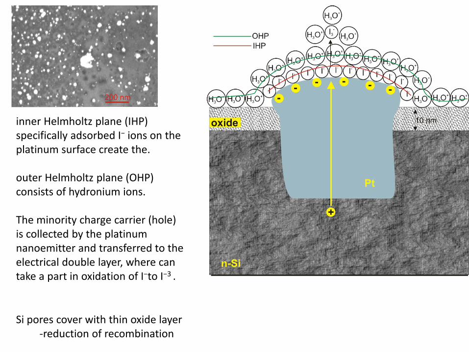
Si pores cover with thin oxide layer -reduction of recombination
inner Helmholtz plane (IHP) specifically adsorbed I− ions on the platinum surface create the. outer Helmholtz plane (OHP) consists of hydronium ions. The minority charge carrier (hole) is collected by the platinum nanoemitter and transferred to the electrical double layer, where can take a part in oxidation of I−to I−3 .
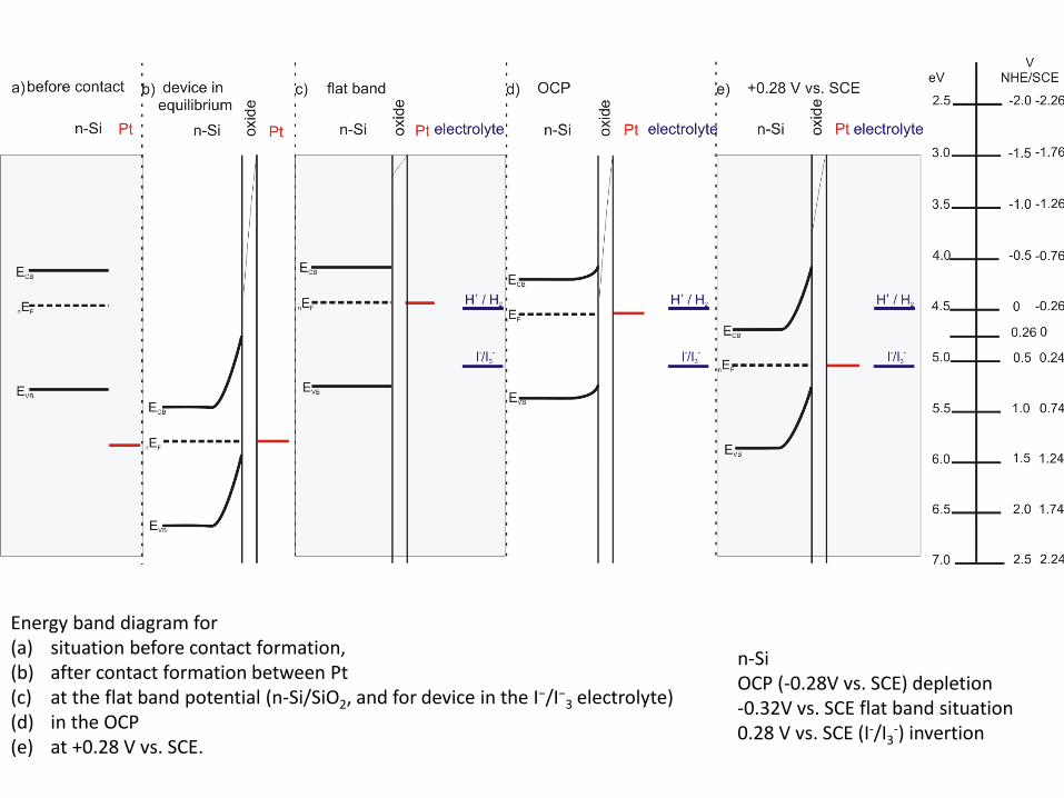
Energy band diagram for (a) situation before contact formation, (b) after contact formation between Pt (c) at the flat band potential (n-Si/SiO2, and for device in the I−/I−
3 electrolyte) (d) in the OCP (e) at +0.28 V vs. SCE.
n-Si OCP (-0.28V vs. SCE) depletion -0.32V vs. SCE flat band situation 0.28 V vs. SCE (I-/I3
-) invertion
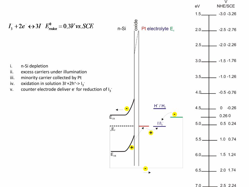
i. n-Si depletion ii. excess carriers under illumination iii. minority carrier collected by Pt iv. oxidation in solution 3I-+2h+-> I3
-
v. counter electrode deliver e- for reduction of I3-
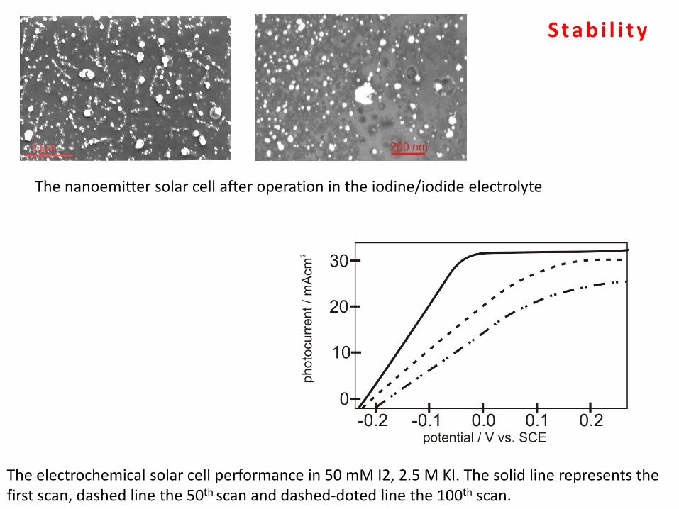
The electrochemical solar cell performance in 50 mM I2, 2.5 M KI. The solid line represents the first scan, dashed line the 50th scan and dashed-doted line the 100th scan.
The nanoemitter solar cell after operation in the iodine/iodide electrolyte
S t a b i l i t y
p-Si based device for H2 evolution
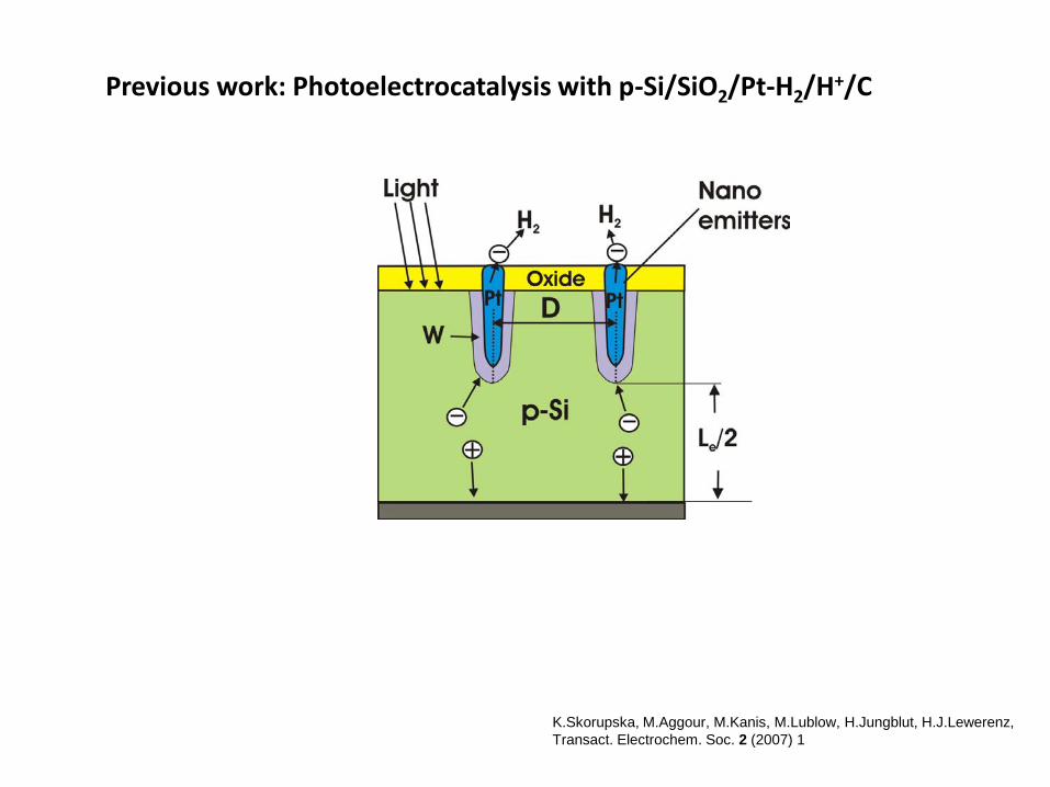
Previous work: Photoelectrocatalysis with p-Si/SiO2/Pt-H2/H+/C
K.Skorupska, M.Aggour, M.Kanis, M.Lublow, H.Jungblut, H.J.Lewerenz, Transact. Electrochem. Soc. 2 (2007) 1
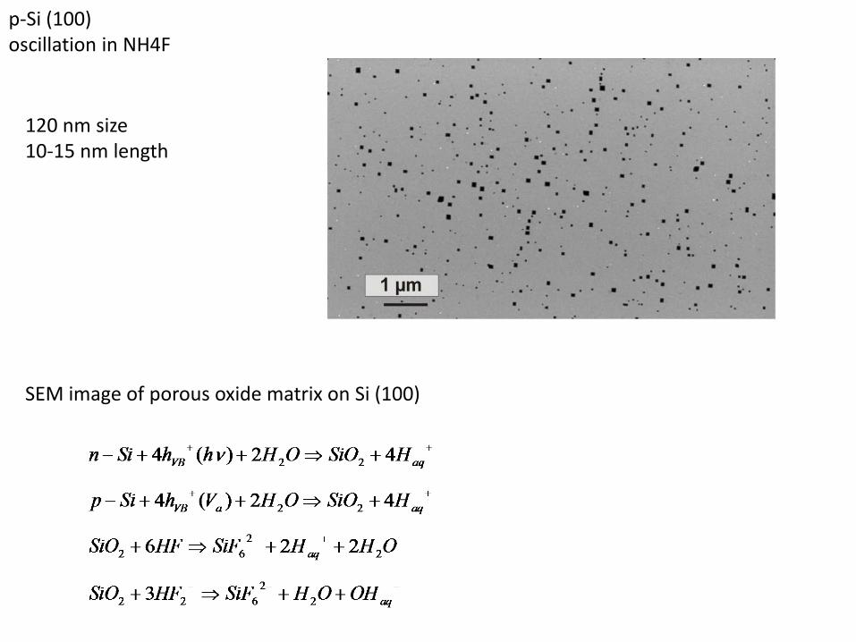
SEM image of porous oxide matrix on Si (100)
p-Si (100) oscillation in NH4F
120 nm size 10-15 nm length
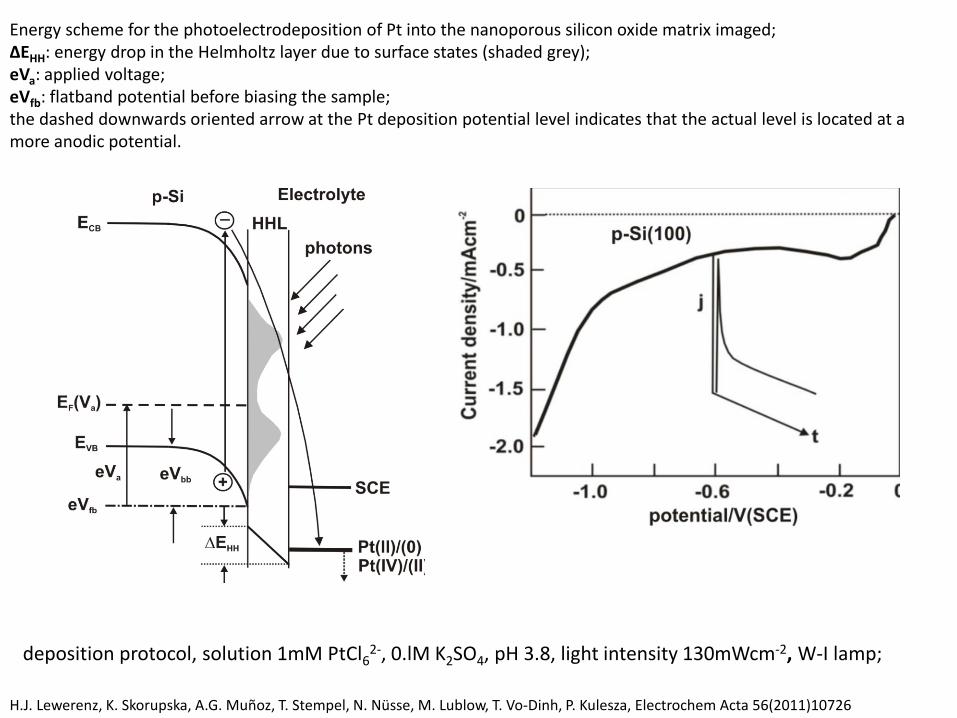
Energy scheme for the photoelectrodeposition of Pt into the nanoporous silicon oxide matrix imaged; ΔEHH: energy drop in the Helmholtz layer due to surface states (shaded grey); eVa: applied voltage; eVfb: flatband potential before biasing the sample; the dashed downwards oriented arrow at the Pt deposition potential level indicates that the actual level is located at a more anodic potential.
H.J. Lewerenz, K. Skorupska, A.G. Muñoz, T. Stempel, N. Nüsse, M. Lublow, T. Vo-Dinh, P. Kulesza, Electrochem Acta 56(2011)10726
deposition protocol, solution 1mM PtCl62-, 0.lM K2SO4, pH 3.8, light intensity 130mWcm-2, W-I lamp;
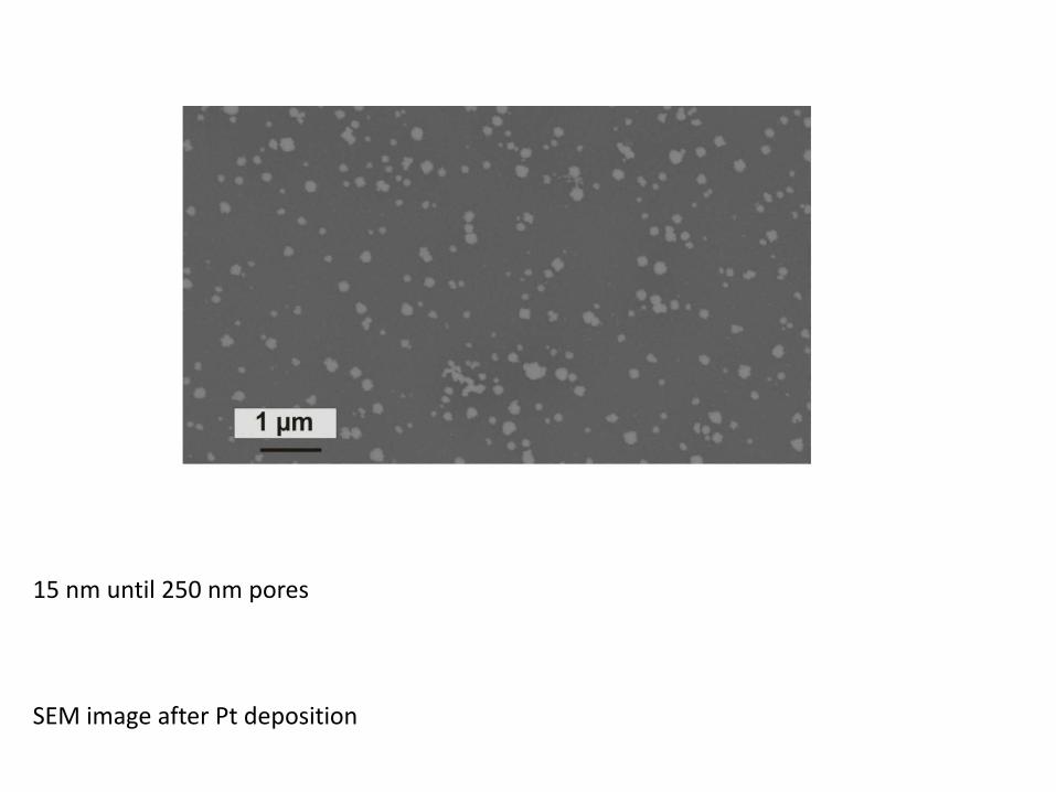
SEM image after Pt deposition
15 nm until 250 nm pores
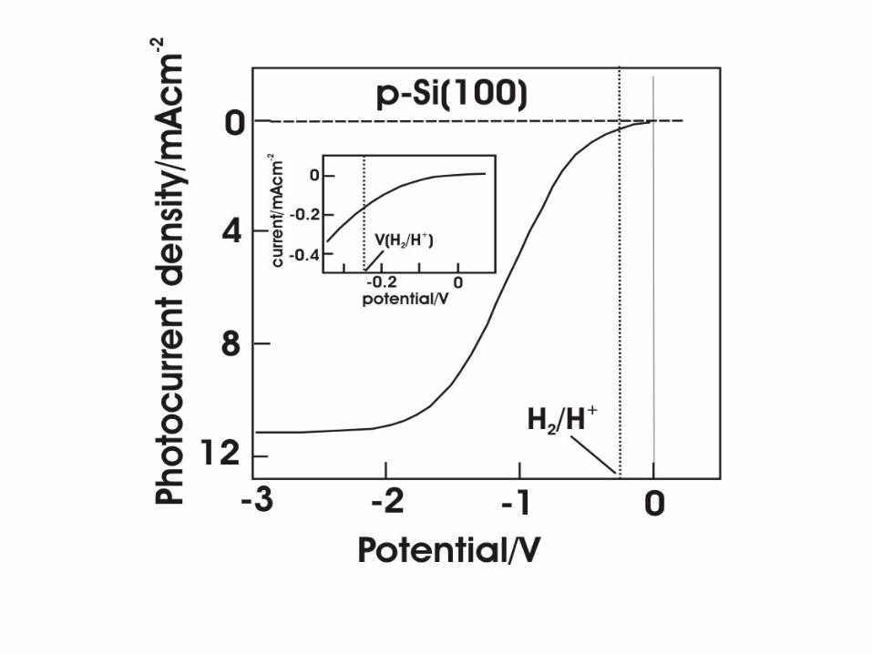
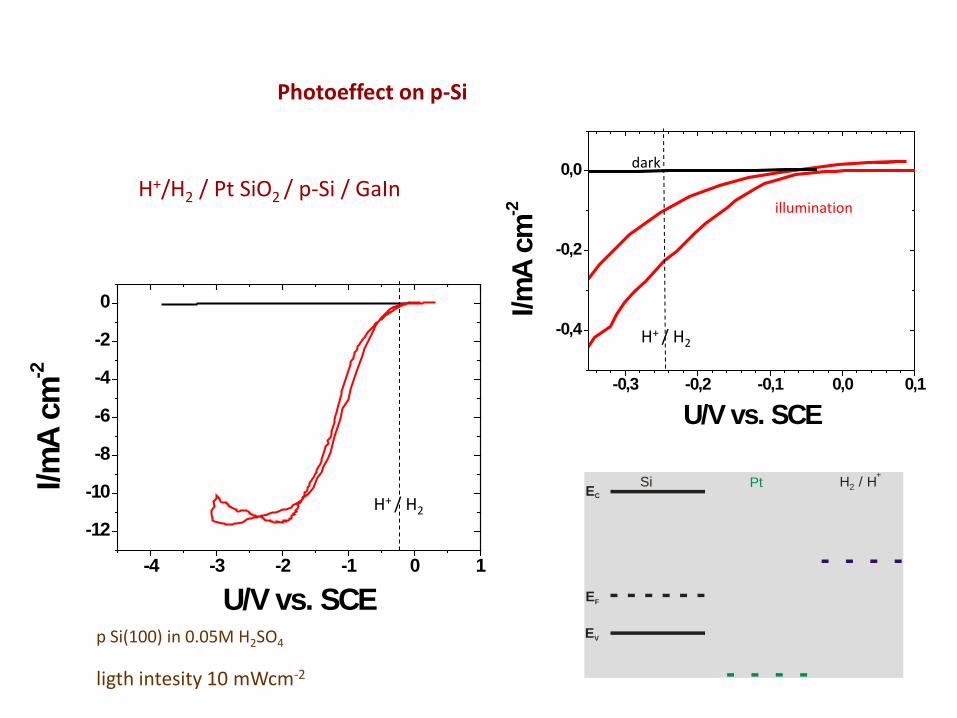
p Si(100) in 0.05M H2SO4
-4 -3 -2 -1 0 1
-12
-10
-8
-6
-4
-2
0
I/mA
cm-2
U/V vs. SCE
-0,3 -0,2 -0,1 0,0 0,1
-0,4
-0,2
0,0
I/mA
cm-2
U/V vs. SCE
Photoeffect on p-Si
H+/H2 / Pt SiO2 / p-Si / GaIn
H+ / H2
H+ / H2
ligth intesity 10 mWcm-2
dark
illumination
Si PtEC
EF
EV
H / H2+


![Solar Photovoltaic (PV) Cells 2 on solar PV [Compatibility Mode].pdf · Solar Photovoltaic (PV) Cells A supplement topic to: Micro-opti l Stical Sensors - A MEMS for electric power](https://static.documents.pub/doc/80x56/5a7150997f8b9a9d538cc26f/solar-photovoltaic-pv-cellswwwengrsjsuedutrhsuchapter-2-on-solar-pv-compatibility.jpg)


