Photovoltaics: Crystalline Si Solar Cells Prof. Antonella Glisenti - Dip. Scienze Chimiche - Università degli Studi di Padova Laurea Magistrale in Scienza dei Materiali Materiali Inorganici Funzionali
Transcript
Photovoltaics:Crystalline Si Solar Cells
Prof. Antonella Glisenti - Dip. Scienze Chimiche - Università degli Studi di Padova
Laurea Magistrale in Scienza dei MaterialiMateriali Inorganici Funzionali
Bibliography
A. Luque, S. Hegedus, Handbook of Photovoltaic Science and Engineering Wiley
Heavily doped regions under the metal: p-type forhole and n-type for electron extraction
(EMITTER, BACK SURFACE FIELD o BSF)
Contacts are required to extract the photogeneratedcarriers from the absorbing semiconductor substrate
SELECTIVE: they should allow one type of carrier to flow from Si to metal without energy loss while blocking the transport of carriers of the opposite type
SURFACES: Contacts
To minimize recombination the thickness of the layershould be much higher than the minority-carrier diffusionlength
P is used for n-contacts; Al alloying has the advantagesover boron that gettering action is achieved
Reduction of the density of electron states in the gap by depositing or growing a layer of insulator
Because of the alteration of the bonding of Si atoms, a largenumber of band gap states exist at a bare Si surface which, acting as SRH recombination centers, make the SRV verylarge (105 cm/s)
SURFACES: Non-contacts
Thermal SiOx grown in an oxygen-rich atmosphere at the expense of substrate Si atoms at about 1000°C
SiNx deposited by PECVD at 300-400°C
Crystalline Si Solar Cells
The optimum cell should use intrinsic material, tominimize Auger recombination and free-carrier
absorption, should be free of defects, should havea thickness capable of minimize recombination
Il could attain nearly 29-30 % efficiency at one sun AM1.5global at 25°C
CELL STRUCTURE
CELL STRUCTURE1. No reflection losses and maximum absorption as achieved by
ideal light –trapping techniques2. Minimum recombination (SRH and surface recombination are
assumed avoidable, only Auger recombination remains)3. The contacts are ideal: neither shading nor series resistance
losses4. No transport losses in the substrate: the carrier profiles in the
substrate are flat
Contacting structures: a) bothcontacts at the front, and b) at the back; c) both facescontacted, d) one carrierextracted at both faces. The structures with interchanged n-and p-types are also possible
23%24%
15%
EMITTERS
Different emitter structures: a) homogeneous emitter withoutsurface passivation; b) homogeneous emitter with surface
passivation; c) selective emitter, d) localized emitter
BACK SURFACE
Rear contactstructures: a)
continuous BSF, b) bifacial cell, c)
local BSF, d) localBSF, bifacial cell,
e) selectiveemitter or floating
junctionpassivation, f)
shorted junction at the back face ofindustrial cells
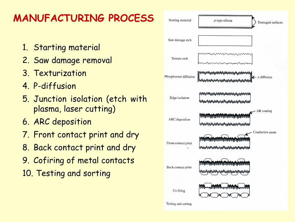
plasma, laser cutting)6. ARC deposition7. Front contact print and dry8. Back contact print and dry9. Cofiring of metal contacts10. Testing and sorting
SAW DAMAGE REMOVAL
The sawing operation leaves the surface of “as-cut” waferswith a high degree of damage: bad surface region, wafer fracture during process
The wafer, in teflon cassetes, are immersed in tankscontaining the etching solution (alkaline)
CELL OPTICS: texturing and light trappingIn a textured face a ray can be reflected toward a neighboring pyramid and hence absorption is enhanced
Texturing is incorporated into both industrial and laboratory Si solar cells and in combination with AR coatings reduces reflectionlosses to a few percent
Photogeneration takes place closer to the collection junction
Effects of surface texturing: a) decreased reflection, b) increased photogeneration in the base
TEXTURIZATION
NaOH etching leading to microscopic pyramids is commonlyemployed;
The pyramid size must be optimized since very smallpyramids lead to high reflection while very large ones can hinder the formation of the contacts
Concentration, temperature, agitation, time;Alcohol is added to improve homogeneity through an
enhancement of the wettability of the silicon surface (5% NaOH, 80°C, 15 min.)
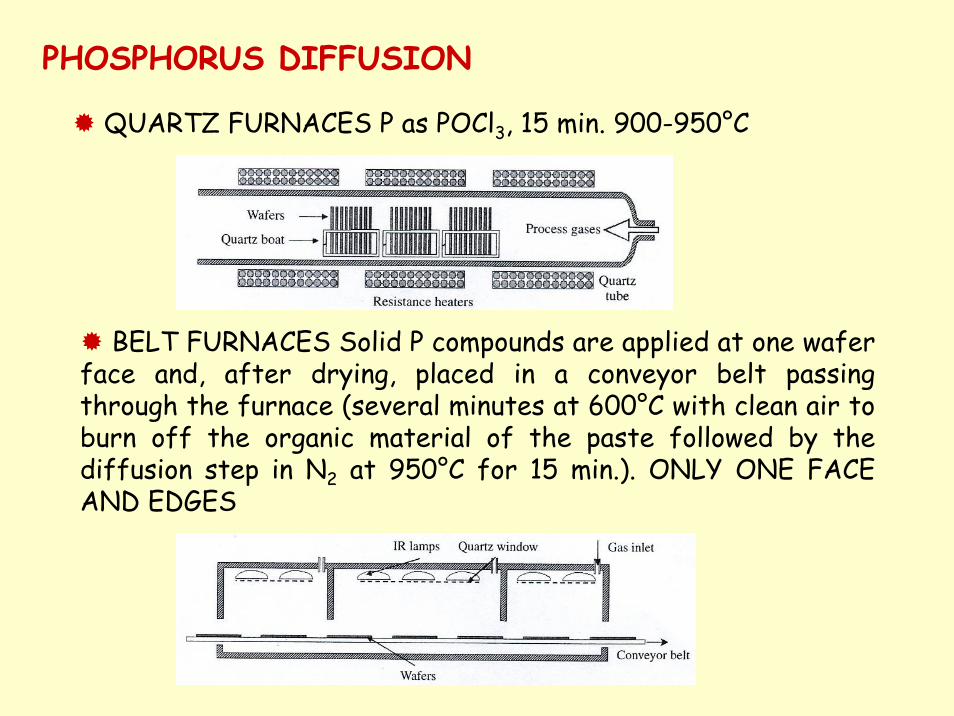
PHOSPHORUS DIFFUSION
QUARTZ FURNACES P as POCl3, 15 min. 900-950°C
BELT FURNACES Solid P compounds are applied at one wafer face and, after drying, placed in a conveyor belt passingthrough the furnace (several minutes at 600°C with clean air toburn off the organic material of the paste followed by the diffusion step in N2 at 950°C for 15 min.). ONLY ONE FACE AND EDGES
Wet etching:Advantagesno damage to the substratehigh throughput and selectivityeasinessDisadvantagesetchant solution into the boundaryprocessing accuracy
Dry etching:Advantagesprocessing accuracyhigh selectivityeasy automationDisadvantagesdamage to the substratelow throughput
CELL OPTICS
1. Shading2. Reflection (30%)
ANTIREFLECTION COATINGSAntireflection coating (ARC) means an optically dielectriclayer desingated to suppress reflection by interferenceeffects
Reflection minimum when thickness is (odd multiple of) nARCλ0/4 (600 nm); reflection = 0 for nARC = average of indexof Si and air
TiOx by CVD (Ti organic compound + water) or spray pyrolisis
SiNx PECVD (also passivating layer)Double layer coatings with λ/4 design with growing indices
from air to silicon (SiZn, MgF2)
Low contact resistance to silicon, low bulk resistivity, low line width, good mechanical adesion, solderability and compatibilitywith the encapsulating materials
silver (too high diffusivity for Cu)
silver + aluminum for the back surface; Al is requiredbecause Ag does not form ohmic contact to p-Si but cannot beused alone because of the difficulty in soldering
FRONT AND BACK CONTACT PRINT AND DRY
Screen printing is a thick-film technology the consists in translating a layer of a material in a desired pattern to the surface of the wafer
SCREENS: (stainless steel wires stretched on a Al frame: 200 wires per inch, wire diameter around 10μm, mesh opening 30 μm - 50% open surface)
PASTES:
SCREEN PRINTING TECHNOLOGY
ORGANIC SOLVENT (must provide fluidity)ORGANIC BINDER (must hold together the active
powder before its thermal activation)CONDUCTING MATERIAL (Ag powder of a size of
tenths of microns; for p-contact Al is also present – 60-80% of the paste)
GLASS FRIT – 5-10 % a powder of different oxides(Pb, Bi, Si, …) with a low melting point and high reactivity at the process temperature that enables movement of the silver grains and etches the silicon surface to allow intimate contact.
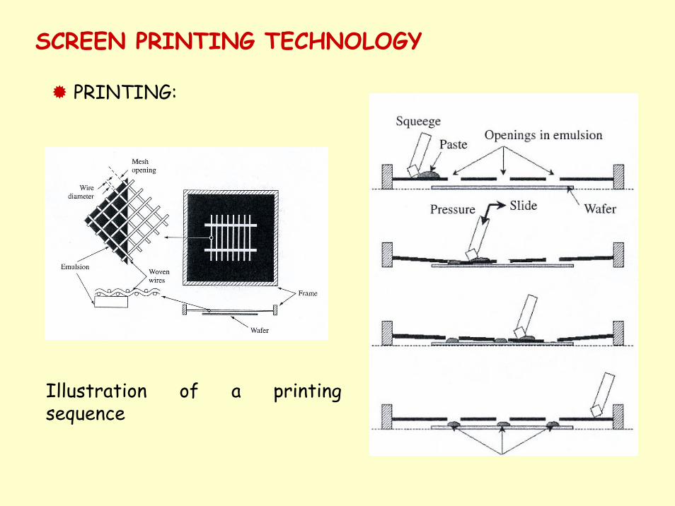
PRINTING:
Illustration of a printingsequence
SCREEN PRINTING TECHNOLOGY
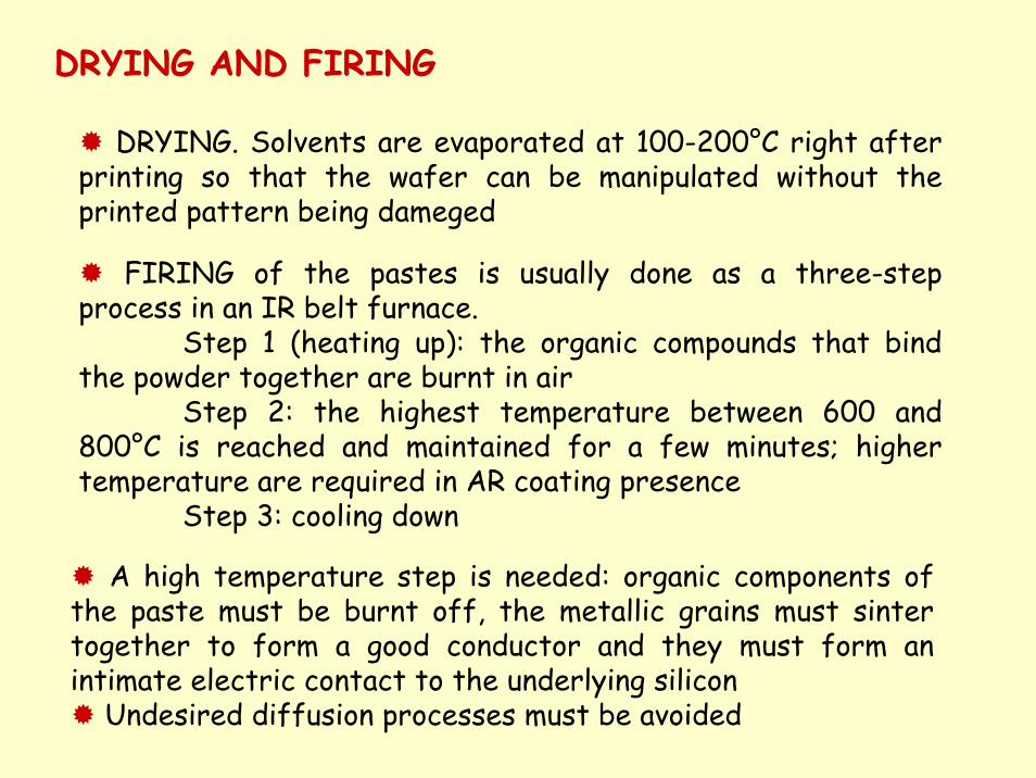
DRYING. Solvents are evaporated at 100-200°C right after printing so that the wafer can be manipulated without the printed pattern being dameged
DRYING AND FIRING
FIRING of the pastes is usually done as a three-stepprocess in an IR belt furnace.
Step 1 (heating up): the organic compounds that bindthe powder together are burnt in air
Step 2: the highest temperature between 600 and 800°C is reached and maintained for a few minutes; highertemperature are required in AR coating presence
Step 3: cooling down
A high temperature step is needed: organic components of the paste must be burnt off, the metallic grains must sintertogether to form a good conductor and they must form anintimate electric contact to the underlying silicon
Undesired diffusion processes must be avoided
The illuminated I-V curve of finished cells is measureunder an artificial light source (sun simulator)
TESTING AND SORTING
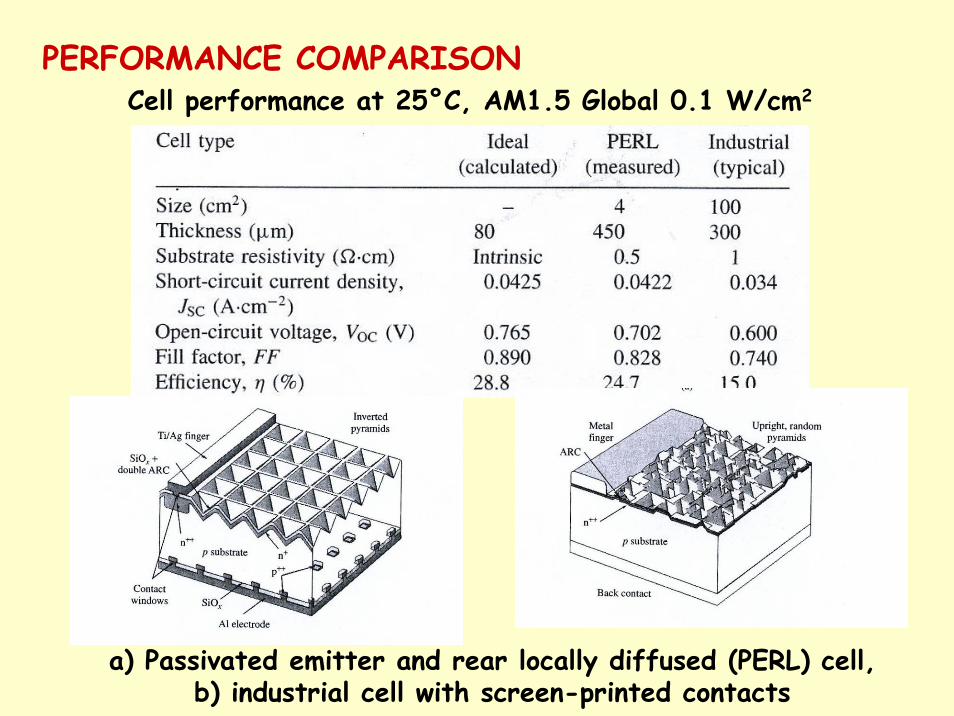
PERFORMANCE COMPARISONCell performance at 25°C, AM1.5 Global 0.1 W/cm2
a) Passivated emitter and rear locally diffused (PERL) cell, b) industrial cell with screen-printed contacts
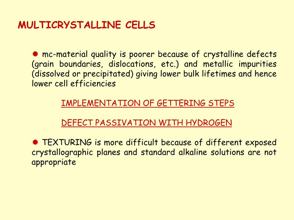
MULTICRYSTALLINE CELLS
mc-material quality is poorer because of crystalline defects(grain boundaries, dislocations, etc.) and metallic impurities(dissolved or precipitated) giving lower bulk lifetimes and hencelower cell efficiencies
IMPLEMENTATION OF GETTERING STEPS
DEFECT PASSIVATION WITH HYDROGEN
TEXTURING is more difficult because of different exposedcrystallographic planes and standard alkaline solutions are notappropriate
PASSIVATION WITH HYDROGENSiNx by PECVD
PECVD for mc-material produces hydrogenation verybenefical for silicon; H interacts with impurity and defects in the bulk of a Si neutralizing their recombination properties to a certain extent (bulk passivation). A thermal step is needed toactivate hydrogenation
Industrial PECVD reactors: a) direct-plasma reactor; b) remote-plasma system
CELL MATRIXIn a module the cells are usually arranged in seriesAfter cell finishing tinned copper ribbons (tabs) are soldered
to the bars at the front; two tabs for cell are employes; seriesinterconnection of strings by soldering the tabs to the rearside of another cell follows.
usually: 36 series-connected cells which under operatingconditions would produce around 15 V at maximum power (12 V)
a) Cell interconnection with tabs; b) two cells in series; c) layout of 36 series-connected cells.
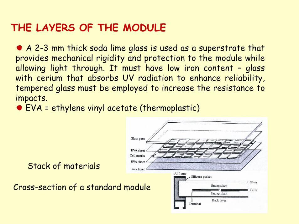
THE LAYERS OF THE MODULE
A 2-3 mm thick soda lime glass is used as a superstrate thatprovides mechanical rigidity and protection to the module whileallowing light through. It must have low iron content – glasswith cerium that absorbs UV radiation to enhance reliability, tempered glass must be employed to increase the resistance toimpacts.
EVA = ethylene vinyl acetate (thermoplastic)
Stack of materials
Cross-section of a standard module
SUBSTRATE:MATERIALS AND PROCESSINGFZ = highest efficiencies
extreme crystalline perfectionlowest contamination levels of metallic and light – O, C, N – impurities) = longest SRH lifetimes
CZ = high concentration of oxygen (low lifetimes)MCZ (Magnetic Czochralski) = low concentration of oxygen
(high efficiencies)mc-Si = crystal defects (grain boundaries and dislocations),
higher content of metallics because of lower segregationto the melt during the fast solidification process (low lifetimes)
The industry uses solar grade CZ-Si wafers, round in origin butvery often trimmed to a pseudo-square shape or multicrystallinesquare wafers. Wafer dimensions are between 10 and 15 cm side and between 200 and350 μm thickness
Doping is p-type boron to a resistivity around 1 Ωcm