Physical and chemical tuning of two-dimensionaltransition metal dichalcogenides
Haotian Wang,a Hongtao Yuan,abc Seung Sae Hong,a Yanbin Lib and Yi Cui*bc
The development of two-dimensional (2D) materials has been experiencing a renaissance since the adventure
of graphene. Layered transition metal dichalcogenides (TMDs) are now playing increasingly important roles in
both fundamental studies and technological applications due to their wide range of material properties from
semiconductors, metals to superconductors. However, a material with fixed properties may not exhibit
versatile applications. Due to the unique crystal structures, the physical and chemical properties of 2D TMDs
can be effectively tuned through different strategies such as reducing dimensions, intercalation,
heterostructure, alloying, and gating. With the flexible tuning of properties 2D TMDs become attractive
candidates for a variety of applications including electronics, optoelectronics, catalysis, and energy.
1. Introduction
Two-dimensional (2D) layered materials with important physicaland chemical properties have been studied for decades. Sincethe recently successful preparation and characterization ofgraphene,1–3 2D materials have attracted a great deal of attentionsince they exhibit novel and intriguing properties with potentialapplications in field effect transistors, optoelectronic devices,
topological insulators, electrocatalysts, and so on.4–16 In the richfamily of 2D materials, layered transition metal dichalcogenides(TMDs) become the focus of fundamental research and techno-logical applications due to their unique crystal structures, a widerange of chemical compositions, and a variety of materialproperties.6,7,11,12,17 2D TMDs are usually denoted MX2, whereM represents a transition metal (such as Ti, V, Nb, Mo, Hf, Ta, W),and X represents the chalcogen (S, Se, and Te). Transition metalsranging from group 4 to group 10 have different numbers ofd-electrons, which fill up the non-bonding d bands to differentlevels, resulting in varied electronic properties includinginsulating, semiconducting, metallic, and superconducting.11
The wide range of electronic structures not only boosts thedevelopment of 2D TMD electronic and optoelectronic devices,
a Department of Applied Physics, Stanford University, Stanford, CA 94305, USAb Department of Materials Science and Engineering, Stanford University, Stanford,
CA 94305, USA. E-mail: [email protected] Stanford Institute for Materials and Energy Sciences, SLAC National Accelerator
Laboratory, 2575 Sand Hill Road, Menlo Park, California 94025, USA
Haotian Wang
Haotian Wang is a graduatestudent in the Department ofApplied Physics at Stanford Uni-versity. He is currently a StanfordInterdisciplinary Graduate Fellow(SIGF). He obtained BS (2011) inPhysics from the University ofScience and Technology of China.He is now supervised by Prof. YiCui and focused on applications oflow-dimensional materials incatalysis, energy storage, andelectronics/optoelectronics. Hongtao Yuan
Hongtao Yuan obtained his PhD(2007) degree from Institute ofPhysics, Chinese Academic ofSciences. He was a postdocresearcher (2007–2009) at TohokuUniversity, and a research associ-ate (2010–2011) and an assistantprofessor (2011–2012) at Quan-tum Phase Electronics Center inthe University of Tokyo. Since2012 he has been a physics scien-tist research associate at GeballeLaboratory for Advanced Materi-als in Stanford University and at
Stanford Institute for Materials and Energy Sciences in SLACNational Accelerator Laboratory, USA.
but also facilitates the applications into catalysis due to thestrong correlation between electronic and catalytic properties.In addition to chemical composition of 2D TMDs, atomicarrangements also play important roles in determining materialproperties. A representative atomic structure of 2D TMDs isshown in Fig. 1(a). The metals and chalcogens are covalentlybonded within the molecular layers, which stack together via theweak van der Waals (vdW) interactions along the z axis to formthe bulk material. The strong intra- and weak inter-layer inter-actions induce the high anisotropy of 2D TMDs, with propertiessuch as facile single layer exfoliation for electronic devices.8
However, the explosive popularity of 2D TMDs does not onlyrely on the intrinsic material properties themselves, but highlydepends on the tunable electronic and catalytic properties.6,7,17
Due to the high anisotropy and unique crystal structure, thematerial properties of 2D TMDs can be effectively tuned in awide regime through different methodologies including reducing
dimensions, intercalation, heterostructure, alloying, gating, pressure,and lighting as illustrated in Fig. 1. For example, the band structuresare significantly changed as we thin down the 2D layers to thesingle-layer limit.8,15–17 Another example is that through theintercalation of guest ions, the carrier densities of 2D TMDs canbe tuned by multiple orders of magnitude.18 Modern technologiesand applications require a wide range of high-quality materialproperties, which can be hardly realized in a single materialwithout any modifications. Therefore, 2D TMDs provide a greatplatform of tuning material properties towards desired func-tions, further attracting a great deal of attention and openingup opportunities for a wide range of applications.
There are a number of important studies and summariesfocused on the attractive properties of 2D TMDs already,6,7,11,19–21
however, the topical review of 2D TMDs’ tunability has not beenproposed yet. Understanding how the material properties can betuned and how these tunable properties can be utilized becomesincreasingly important. In this review, we focus on differentphysical and chemical strategies for tuning 2D TMDs properties,such as band structures, carrier densities, catalytic activities, opticalproperties. In each strategy, how the electronic and catalyticproperties of 2D TMDs are modified is explained in detail, withrepresentative applications included.
2. Dimension tuning2.1 Dimension tuning along the z direction
2D TMD semiconductors with tunable bandgaps through thinningdown the bulk materials to few- or single-layer limits haverecently become a powerful approach for electronic and opticalapplications.8,22–26 As an example, the bulk MoS2 crystal, anindirect bandgap semiconductor of 1.29 eV, consists of vdWbonded S–Mo–S layer units. Each of these stable units (referredto as a MoS2 monolayer) consists of two hexagonal planes of
Yanbin Li
Yanbin Li is a PhD student in theDepartment of Materials Scienceand Engineering at StanfordUniversity supervised by Prof. YiCui. He received his BS degree inphysics from University of Scienceand Technology of China in 2013.His graduate research focuses onthe controlled synthesis of low-dimensional materials.
Yi Cui
Yi Cui is an Associate Professor inthe Department of MaterialsScience and Engineering atStanford University. He obtainedBS (1998) in Chemistry from theUniversity of Science andTechnology of China, PhD (2002)from Harvard University. He wasa Miller Postdoctoral Fellow at theUniversity of California, Berkeleyfrom 2003–2005. He holds a jointappointment in SLAC NationalAccelerator Laboratory. Hiscurrent research is on two-
dimensional layered materials, energy storage, photovoltaic,topological insulators, biology and environment. Yi Cui is anAssociate Editor of Nano Letters. He founded Amprius Inc. in2008, a company to commercialize the high-energy batterytechnology.
Seung Sae Hong
Seung Sae Hong is currently apostdoctoral fellow in the groupof Prof. Harold Y. Hwang atStanford University. He receivedhis BS degree in physics fromSeoul National University andcompleted his PhD degree inapplied physics from StanfordUniversity, supervised by Prof. YiCui. His research interestsinclude physics and materialsscience of low-dimensionalmaterials, with an emphasis onchalcogenide and oxide 2Dmaterials.
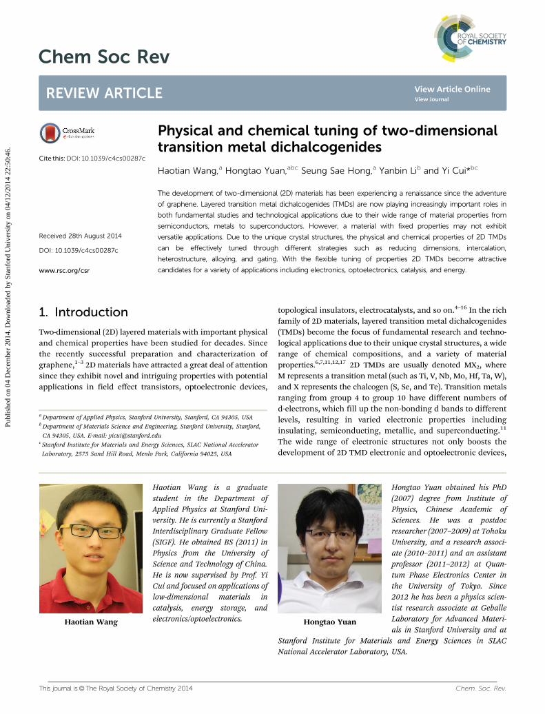
S atoms and an intermediate hexagonal plane of Mo atomscoordinated through ionic-covalent interactions with the S atomsin a trigonal prismatic arrangement. Due to the high anisotropy,single-layer MoS2 can be easily achieved by mechanical cleavage,directly providing the possibility to tune the physical properties atthe 2D monolayer limit. Chemical vapor deposition enables large-area, uniform, and high-quality single-layer 2D TMDs.6,11,27–33 Inaddition, chemical and electrochemical exfoliation of mono-layered TMDs makes it possible to achieve large-scale single layerproduction.34,35 As early as 2007, theorists have predicted thescaling properties in the band structure:36,37 the MoS2 crystalsexhibit a crossover from an indirect to a direct gap semiconductorfrom bulk to its monolayer limit. As an early experimental reporton the thickness dependent physical properties of the MX2 system(Fig. 2),38,39 the evolution of the electronic structure and resultingoptical properties of ultrathin MoS2 crystals was observed as afunction of layer number from 1 to 6 layers by using spectroscopictechniques: optical absorption, photoluminescence (PL), andphotoconductivity (with the thickness characterized by atomic-force microscopy). The combination of these spectroscopicmethods allowed researchers to optically trace the evolutionfrom the indirect to direct bandgaps of the material with thelayer thickness decreasing to the monolayer. The crossover froman indirect gap material to a direct gap material naturally accountsfor the great enhancement of the luminescence observed in
monolayer MoS2. The observed dependence of the bandgap on thelayer number is also in qualitative agreement with band calculations.The controllability of the bandgap may also be used to optimize thematerial’s use as a photocatalyst and for photovoltaic applications.
To experimentally understand the origin of these extraordinaryPL properties, angle-resolved photoemission spectroscopy (ARPES)measurements are carried out to investigate the detailed para-meters of the band structure and also the evolution of the banddispersion with the layer thickness (Fig. 2).40,41 One example isARPES measurement based on monolayer MoSe2 thin films withvariable thickness, grown by molecular beam epitaxy.40 Theband structure measured experimentally indicates a strongertendency of monolayer MoSe2 towards a direct bandgap. As animportant feature of the monolayer MX2, a significant spin-splitting of B180 meV at the valence band maximum of amonolayer MoSe2 film, related to the strong spin orbital inter-action, could be clearly observed experimentally for the firsttime. Other examples are observations on the evolution of thethickness-dependent electronic band structure of the MoS2 andWSe2, based on the combination of the spatial resolution ARPESwith the tape-cleaved or chemical-vapor-deposition-grown ultra-thin samples.41 All these observations provide direct evidence forindirect-to-direct band gap transition in both MoS2 and WSe2
cases (the shifting of the valence band maximum from G to K) asthinning down the sample from the bulk to monolayer.
Fig. 1 (a) Schematic of 2D TMDs. M represents a transition metal, and X represents a chalcogen. (b) Schematic of tuning 2D TMD properties by reducingdimension along the z direction and xy directions. (c) Schematic of tuning 2D TMD properties by guest ion intercalation. (d) Schematic of tuning 2D TMDproperties by constructing heterostructures and alloying. (e) Schematic of tuning 2D TMD properties by gating. (f) Schematic of tuning 2D TMD propertiesby applying high pressure. (g) Schematic of tuning 2D TMD properties by illuminating circularly-polarized light.
Such an unusual electronic structure evolution stems fromthe characters and spatial distribution of d-electron orbitals ofMoS2. Theoretical calculations show that electronic states ofdifferent wave vectors have electron orbitals with differentspatial distributions.38 Specifically, conduction band states at theK point are primarily composed of strongly localized d orbitals atMo atom sites, and they have minimal interlayer coupling since Moatoms are located in the middle of the S–Mo–S unit cell. The statesnear the G point and the point of indirect band-gap originate froma linear combination of d orbitals on Mo atoms and antibonding pz
orbitals on S atoms. The orbitals have strong interlayer couplingand their energies depend sensitively on layer thickness. Such anunderstanding on the direct bandgap feature makes the opticalmeasurement of the band structure available and further paves away for the optical realization of the circularly-polarized lightpumped valley polarization around the band edge at K points.
2.2 Dimension tuning along xy directions
Due to the highly anisotropic structures, 2D TMD materials tendto grow fast within the layer to form different morphologies such
Fig. 2 (a) Calculated band structures of bulk MoS2, quadrilayer MoS2, bilayer MoS2 and monolayer MoS2. The solid arrows indicate the lowest energy transitions.Bulk MoS2 is characterized by an indirect bandgap. The direct excitonic transitions occur at high energies at the K point. With reduced layer thickness, the indirectbandgap becomes larger, while the direct excitonic transition barely changes. For monolayer MoS2, it becomes a direct bandgap semiconductor. This dramaticchange in electronic structure in monolayer MoS2 can explain the observed jump in monolayer photoluminescence efficiency. Reproduced with permission fromref. 38. Copyright 2010, American Chemical Society. (b) PL spectra of mono- and bilayer MoS2 samples in the photon energy range from 1.3 to 2.2 eV. Inset: PLquantum yield of thin layers (1–6 layers). Reproduced with permission from ref. 39. Copyright 2010, American Physical Society. (c) Band evolution with increasingthickness of MoSe2 thin films. ARPES spectra and second-derivative spectra of monolayer, bilayer, trilayer and 8 ML MoSe2 thin films along the G–K direction. Whiteand green dotted lines indicate the energy positions of the apices of valence bands at the G and K points, respectively, with energy values written in the samecolors. Reproduced with permission from ref. 41. Copyright 2013, Nature Publishing Group.
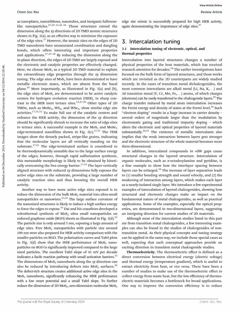
as nanoplates, nanoribbons, nanotubes, and inorganic fullerene-like nanoparticles.27,29–31,42–44 Those structures extend thedimension along the xy directions of 2D TMD atomic structuresshown in Fig. 1(a), as an effective way to minimize the exposureof the edge sites.17 However, the atomic sites on the edges of 2DTMD nanosheets have unsaturated coordination and danglingbonds, which offers interesting and important propertiesand applications.17,45–49 By reducing the dimension along thein-plane direction, the edges of 2D TMD are largely exposed andthe electronic and catalytic properties are effectively changed.Here, we choose MoS2 as a typical 2D TMD material to explainthe extraordinary edge properties through the xy dimensiontuning. The edge sites of MoS2 have been demonstrated to havemetallic electronic states, which are absent from the basalplane.45 More importantly, as illustrated in Fig. 3(a) and (b),the edge sites of MoS2 are demonstrated to be active catalyticcenters for hydrogen evolution reaction (HER), in sharp con-trast to the HER inert terrace sites.12,47,50 Other types of 2DTMDs, such as MoSe2, WS2, and WSe2, show similar edge siteactivities.17,51,52 To make full use of the catalytic centers andenhance the HER activity, the dimension of the xy directionshould be significantly shrunk to increase the ratio of edge sitesto terrace sites. A successful example is the MoS2 and MoSe2
edge-terminated nanofilms shown in Fig. 3(c).17,51 The TEMimages show the densely packed, stripe-like grains, indicatingthat the molecular layers are all vertically standing on thesubstrate.17,51 The edge-terminated surface is considered tobe thermodynamically unstable due to the large surface energyof the edges; however, through rapid sulfurization synthesis,this metastable morphology is likely to be obtained by kineti-cally overcoming the free energy barrier.17,51 The layer verticallyaligned structure with reduced xy dimensions fully exposes theactive edge sites on the substrate, providing a large number ofcatalytic reaction sites and thus boosting the overall HERactivity.
Another way to have more active edge sites exposed is toreduce the dimension of the bulk MoS2 material into ultra-smallnanoparticles or nanowires.53,54 The large surface curvature ofthe nanosized structures is likely to induce a high surface energyto force the edges to expose.55 Dai and his coauthors developed asolvothermal synthesis of MoS2 ultra small nanoparticles onreduced graphene oxide (RGO) sheets as illustrated in Fig. 3(d).53
The particle size is only around 5 nm, exposing a large amount ofedge sites. Free MoS2 nanoparticles with particle size around100 nm were also prepared for HER activity comparison with thesmaller particles on RGO. The polarization curves and Tafel plotsin Fig. 3(d) show that the HER performance of MoS2 nano-particles on RGO is significantly improved compared to the largesized particles. The excellent Tafel slope of 41 mV per decadeindicates a facile reaction pathway with small activation barriers.53
The dimensions of MoS2 nanosheets along the xy direction canalso be reduced by introducing defects into MoS2 surfaces.56
The defect-rich structure creates additional active edge sites in theMoS2 nanosheets, significantly enhancing the HER performancewith a low onset potential and a small Tafel slope. To furtherreduce the dimension of 2D MoS2, zero-dimension molecular MoS2
edge site mimic is successfully prepared for high HER activity,again demonstrating the importance of edge sites.57
3. Intercalation tuning3.1 Intercalation tuning of electronic, optical, andthermal properties
Intercalation into layered structures changes a number ofphysical properties of the host materials, which has receivedresearch attention for decades.18 The earlier investigations havefocused on the bulk form of layered structures, and those workswhich are revisited as the 2D counterparts are widely studiedrecently. In the cases of transition metal dichalcogenides, themost common intercalants are alkali metal (Li, Na, K,. . .) and3d transition metal (V, Cr, Mn, Fe,. . .) atoms, of which charges(electrons) can be easily transferred to the chalcogenide layers.19 Thecharge transfer induced by metal atom intercalation increasesthe Fermi energy and density of states at the Fermi level.18 Such‘‘electron doping’’ results in a huge increase in carrier density –several orders of magnitude larger than the modulation byelectrostatic gating and traditional impurity doping – whichalters the electronic and optical properties of layered materialssubstantially.18,19 The existence of metallic intercalants alsoimplies that the weak interaction between layers gets strongerand the electronic structure of the whole material becomes morethree-dimensional.
In addition, intercalated compounds in vdW gaps causestructural changes in the layered structure. Intercalation oforganic molecules, such as n-octadecylamine and pyridine, isa fine example to show how the interlayer spacing betweenlayers can be enlarged.58 The increase of layer separation leadsto (1) smaller bonding strength and sound velocity, and (2) theweakening of interaction among layers, which makes each layeras a nearly-isolated single layer. We introduce a few experimentalexamples of intercalation of layered chalcogenides, showing howstructural and electronic changes make an impact on thefundamental nature of metal chalcogenides, as well as practicalapplications. Some of the examples, especially the optical prop-erties, are demonstrated in two-dimensional layers, suggestingan intriguing direction for current studies of 2D materials.
Although most of the intercalation studies listed in this partare from transition metal chalcogenides, a few interesting exam-ples can also be found in the studies of chalcogenides of non-transition metal. As their physical concepts and tuning strategycan be applied in the same way, we include those special cases aswell, expecting that such conceptual approaches provide anexciting direction in transition metal chalcogenide studies.
Thermoelectricity. The thermoelectric effect is defined as adirect conversion between electrical energy (electric voltage)and thermal energy (temperature gradient), which is useful toextract electricity from heat, or vice versa. There have been anumber of studies to make use of the thermoelectric effect tocollect energy from waste heat, but the low efficiency of thermo-electric materials becomes a bottleneck for broad applications.One way to improve the conversion efficiency is to reduce
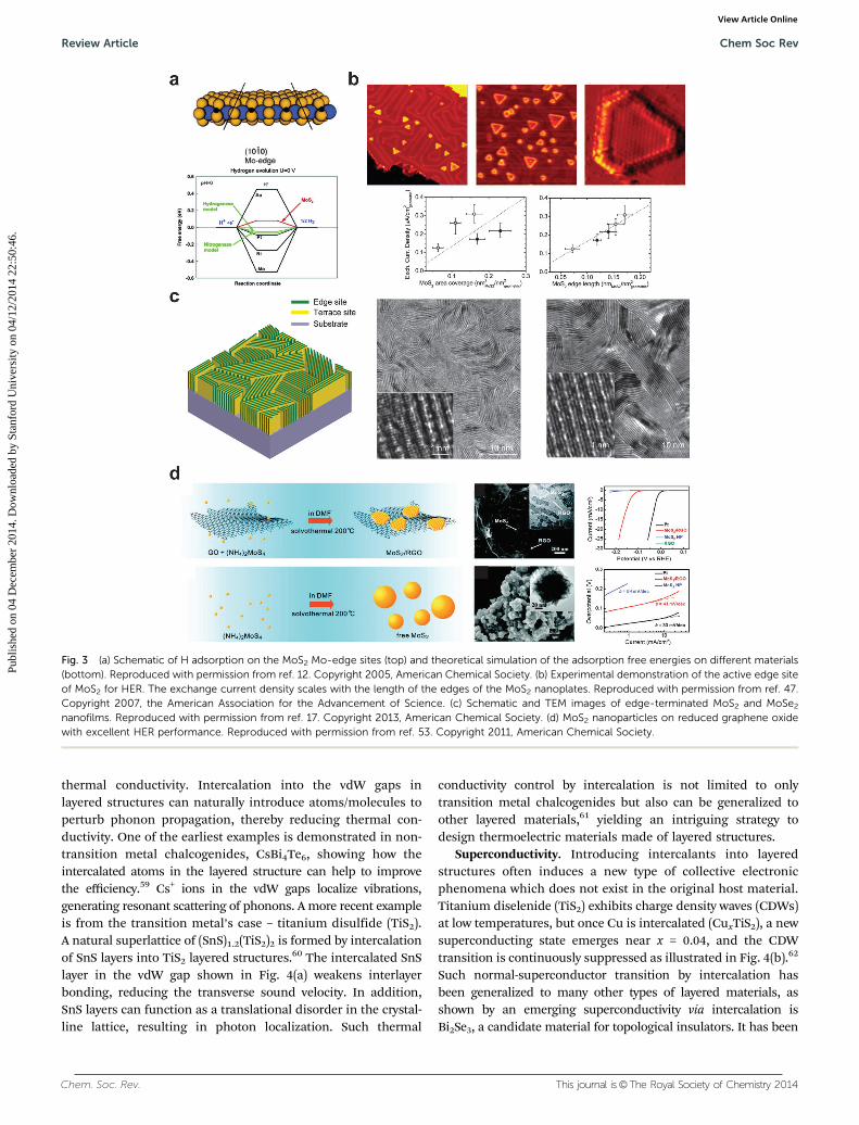
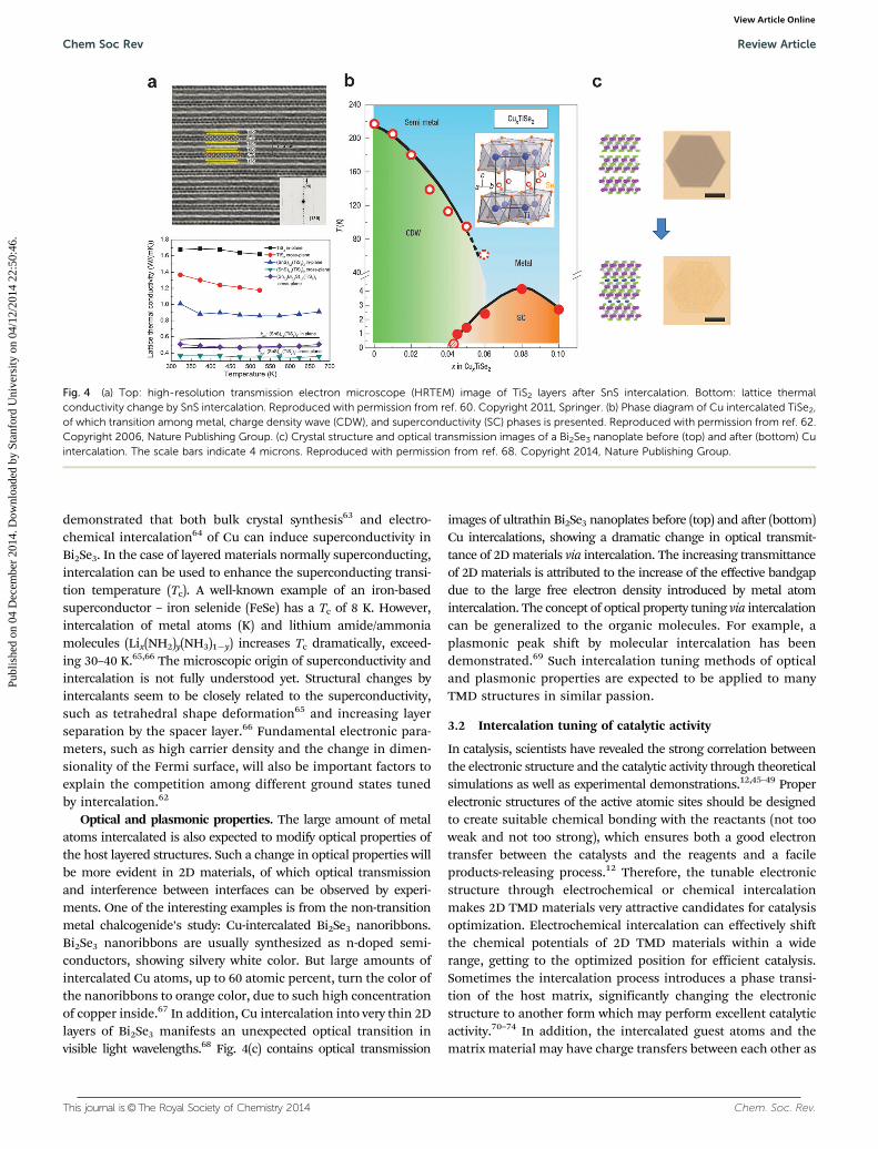
thermal conductivity. Intercalation into the vdW gaps inlayered structures can naturally introduce atoms/molecules toperturb phonon propagation, thereby reducing thermal con-ductivity. One of the earliest examples is demonstrated in non-transition metal chalcogenides, CsBi4Te6, showing how theintercalated atoms in the layered structure can help to improvethe efficiency.59 Cs+ ions in the vdW gaps localize vibrations,generating resonant scattering of phonons. A more recent exampleis from the transition metal’s case – titanium disulfide (TiS2).A natural superlattice of (SnS)1.2(TiS2)2 is formed by intercalationof SnS layers into TiS2 layered structures.60 The intercalated SnSlayer in the vdW gap shown in Fig. 4(a) weakens interlayerbonding, reducing the transverse sound velocity. In addition,SnS layers can function as a translational disorder in the crystal-line lattice, resulting in photon localization. Such thermal
conductivity control by intercalation is not limited to onlytransition metal chalcogenides but also can be generalized toother layered materials,61 yielding an intriguing strategy todesign thermoelectric materials made of layered structures.
Superconductivity. Introducing intercalants into layeredstructures often induces a new type of collective electronicphenomena which does not exist in the original host material.Titanium diselenide (TiS2) exhibits charge density waves (CDWs)at low temperatures, but once Cu is intercalated (CuxTiS2), a newsuperconducting state emerges near x = 0.04, and the CDWtransition is continuously suppressed as illustrated in Fig. 4(b).62
Such normal-superconductor transition by intercalation hasbeen generalized to many other types of layered materials, asshown by an emerging superconductivity via intercalation isBi2Se3, a candidate material for topological insulators. It has been
Fig. 3 (a) Schematic of H adsorption on the MoS2 Mo-edge sites (top) and theoretical simulation of the adsorption free energies on different materials(bottom). Reproduced with permission from ref. 12. Copyright 2005, American Chemical Society. (b) Experimental demonstration of the active edge siteof MoS2 for HER. The exchange current density scales with the length of the edges of the MoS2 nanoplates. Reproduced with permission from ref. 47.Copyright 2007, the American Association for the Advancement of Science. (c) Schematic and TEM images of edge-terminated MoS2 and MoSe2
nanofilms. Reproduced with permission from ref. 17. Copyright 2013, American Chemical Society. (d) MoS2 nanoparticles on reduced graphene oxidewith excellent HER performance. Reproduced with permission from ref. 53. Copyright 2011, American Chemical Society.
demonstrated that both bulk crystal synthesis63 and electro-chemical intercalation64 of Cu can induce superconductivity inBi2Se3. In the case of layered materials normally superconducting,intercalation can be used to enhance the superconducting transi-tion temperature (Tc). A well-known example of an iron-basedsuperconductor – iron selenide (FeSe) has a Tc of 8 K. However,intercalation of metal atoms (K) and lithium amide/ammoniamolecules (Lix(NH2)y(NH3)1�y) increases Tc dramatically, exceed-ing 30–40 K.65,66 The microscopic origin of superconductivity andintercalation is not fully understood yet. Structural changes byintercalants seem to be closely related to the superconductivity,such as tetrahedral shape deformation65 and increasing layerseparation by the spacer layer.66 Fundamental electronic para-meters, such as high carrier density and the change in dimen-sionality of the Fermi surface, will also be important factors toexplain the competition among different ground states tunedby intercalation.62
Optical and plasmonic properties. The large amount of metalatoms intercalated is also expected to modify optical properties ofthe host layered structures. Such a change in optical properties willbe more evident in 2D materials, of which optical transmissionand interference between interfaces can be observed by experi-ments. One of the interesting examples is from the non-transitionmetal chalcogenide’s study: Cu-intercalated Bi2Se3 nanoribbons.Bi2Se3 nanoribbons are usually synthesized as n-doped semi-conductors, showing silvery white color. But large amounts ofintercalated Cu atoms, up to 60 atomic percent, turn the color ofthe nanoribbons to orange color, due to such high concentrationof copper inside.67 In addition, Cu intercalation into very thin 2Dlayers of Bi2Se3 manifests an unexpected optical transition invisible light wavelengths.68 Fig. 4(c) contains optical transmission
images of ultrathin Bi2Se3 nanoplates before (top) and after (bottom)Cu intercalations, showing a dramatic change in optical transmit-tance of 2D materials via intercalation. The increasing transmittanceof 2D materials is attributed to the increase of the effective bandgapdue to the large free electron density introduced by metal atomintercalation. The concept of optical property tuning via intercalationcan be generalized to the organic molecules. For example, aplasmonic peak shift by molecular intercalation has beendemonstrated.69 Such intercalation tuning methods of opticaland plasmonic properties are expected to be applied to manyTMD structures in similar passion.
3.2 Intercalation tuning of catalytic activity
In catalysis, scientists have revealed the strong correlation betweenthe electronic structure and the catalytic activity through theoreticalsimulations as well as experimental demonstrations.12,45–49 Properelectronic structures of the active atomic sites should be designedto create suitable chemical bonding with the reactants (not tooweak and not too strong), which ensures both a good electrontransfer between the catalysts and the reagents and a facileproducts-releasing process.12 Therefore, the tunable electronicstructure through electrochemical or chemical intercalationmakes 2D TMD materials very attractive candidates for catalysisoptimization. Electrochemical intercalation can effectively shiftthe chemical potentials of 2D TMD materials within a widerange, getting to the optimized position for efficient catalysis.Sometimes the intercalation process introduces a phase transi-tion of the host matrix, significantly changing the electronicstructure to another form which may perform excellent catalyticactivity.70–74 In addition, the intercalated guest atoms and thematrix material may have charge transfers between each other as
Fig. 4 (a) Top: high-resolution transmission electron microscope (HRTEM) image of TiS2 layers after SnS intercalation. Bottom: lattice thermalconductivity change by SnS intercalation. Reproduced with permission from ref. 60. Copyright 2011, Springer. (b) Phase diagram of Cu intercalated TiSe2,of which transition among metal, charge density wave (CDW), and superconductivity (SC) phases is presented. Reproduced with permission from ref. 62.Copyright 2006, Nature Publishing Group. (c) Crystal structure and optical transmission images of a Bi2Se3 nanoplate before (top) and after (bottom) Cuintercalation. The scale bars indicate 4 microns. Reproduced with permission from ref. 68. Copyright 2014, Nature Publishing Group.
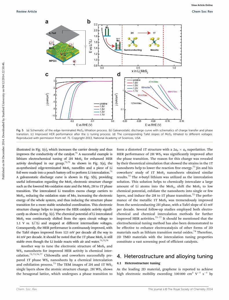
illustrated in Fig. 1(c), which increases the carrier density and thusimproves the conductivity of the catalyst.71 A successful example islithium electrochemical tuning of 2H MoS2 for enhanced HERactivity developed in our group.71,75 As shown in Fig. 5(a), theas-synthesized edge-terminated MoS2 nanofilm and a piece of Lifoil were made into a pouch battery cell to perform Li intercalation.71
A galvanostatic discharge curve is shown in Fig. 5(b), providinguseful information regarding the MoS2 electronic structure changesuch as the lowered Mo oxidation state and the MoS2 2H to 1T phasetransition. The intercalated Li transfers excess charge carriers toMoS2, reducing the oxidation state of Mo, increasing the electronicenergy of the whole system, and thus inducing the structure phasetransition for a more stable octahedral coordination. This electronicstructure change helps to improve the HER catalytic activity signifi-cantly as shown in Fig. 5(c). The chemical potential of Li intercalatedMoS2 was continuously shifted from the open circuit voltage to1.1 V vs. Li+/Li and stopped at different intermediate voltages.Consequently, the HER performance is continuously improved, withthe Tafel slopes improved from 123 mV per decade all the way to44 mV per decade. It should be noted that the 1T phase MoS2 is stillstable even though the Li inside reacts with air and water.71,75,76
Another way to tune the electronic structure of MoS2 andWS2 nanosheets for improved HER activity is chemical inter-calation.72,73,76,77 Chhowalla and coworkers successfully pre-pared 1T phase WS2 nanosheets by a chemical intercalationand exfoliation process.73 The TEM images of 2H and 1T WS2
single layers show the atomic structure change. 2H WS2 showsthe hexagonal lattice, which undergoes a phase transition to
form a distorted 1T structure with a 2a0 � a0 superlattice. TheHER performance of 2H WS2 was significantly improved afterthe phase transition. The reason for this change was revealedby their theoretical simulation that showed the strains in the 1Tnanosheets help to lower the reaction free energy.73 Jin and hiscoworkers’ study of 1T MoS2 nanosheets obtained similarresults.72 The n-butyl lithium was utilized as the intercalationsolution. This solution helps to chemically intercalate a largeamount of Li atoms into the MoS2, shift the MoS2 to lowchemical potential, exfoliate the nanosheets into single or fewlayers, and induce the 2H to 1T phase transition.72 The perfor-mance of the metallic 1T MoS2 was tremendously improvedfrom the semiconducting 2H phase, with a Tafel slope of 43 mVper decade. Several follow-up studies employed both electro-chemical and chemical intercalation methods for furtherimproved HER activities.75–77 It should be mentioned that theelectrochemical tuning method has also been demonstrated tobe effective to enhance electrocatalysis of other forms of 2Dmaterials such as lithium transition metal oxides.74 Therefore,2D TMD materials with the intercalation tuning propertiesconstitute a vast screening pool of efficient catalysts.
4. Heterostructure and alloying tuning4.1 Heterostructure tuning
As the leading 2D material, graphene is reported to achievehigh electronic mobility exceeding 100 000 cm2 V�1 s�1 by
Fig. 5 (a) Schematic of the edge-terminated MoS2 lithiation process. (b) Galvanostatic discharge curve with schematics of charge transfer and phasetransition. (c) Improved HER performance after the Li tuning process. (d) The corresponding Tafel slopes of MoS2 lithiated to different voltages.Reproduced with permission from ref. 71. Copyright 2013, National Academy of Sciences, USA.
artificially stacking graphene on top of hBN to form a hetero-structure.78 This work first attracted attention to tuning theproperties of 2D materials via forming heterostructures frommaterials with different bandgaps and work functions.6 Inaddition, graphene/h-BN heterostructure also demonstratesmore exotic physics, known as Hofstadter’s butterfly. Similar tographite, TMDs MX2 crystallizes in a vertically stacked, weaklyinteracted layered structure. Hence, the individual monolayers canbe mechanically exfoliated by the simple Scotch-tape technique,2
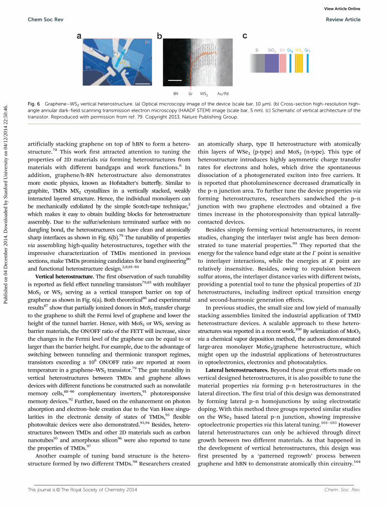
which makes it easy to obtain building blocks for heterostructureassembly. Due to the sulfur/selenium terminated surface with nodangling bond, the heterostructures can have clean and atomicallysharp interfaces as shown in Fig. 6(b).79 The tunability of propertiesvia assembling high-quality heterostructures, together with theimpressive characterization of TMDs mentioned in previoussections, make TMDs promising candidates for band engineering80
and functional heterostructure design.2,8,81–84
Vertical heterostructure. The first observation of such tunabilityis reported as field effect tunneling transistors79,85 with multilayerMoS2 or WS2 serving as a vertical transport barrier on top ofgraphene as shown in Fig. 6(a). Both theoretical86 and experimentalresults87 show that partially ionized donors in MoS2 transfer chargeto the graphene to shift the Fermi level of graphene and lower theheight of the tunnel barrier. Hence, with MoS2 or WS2 serving asbarrier materials, the ON/OFF ratio of the FETT will increase, sincethe changes in the Fermi level of the graphene can be equal to orlarger than the barrier height. For example, due to the advantage ofswitching between tunneling and thermionic transport regimes,transistors exceeding a 106 ON/OFF ratio are reported at roomtemperature in a graphene–WS2 transistor.79 The gate tunability invertical heterostructures between TMDs and graphene allowsdevices with different functions be constructed such as nonvolatilememory cells,88–90 complementary inverters,91 photoresponsivememory devices.92 Further, based on the enhancement on photonabsorption and electron–hole creation due to the Van Hove singu-larities in the electronic density of states of TMDs,93 flexiblephotovoltaic devices were also demonstrated.93,94 Besides, hetero-structures between TMDs and other 2D materials such as carbonnanotubes95 and amorphous silicon96 were also reported to tunethe properties of TMDs.97
Another example of tuning band structure is the hetero-structure formed by two different TMDs.98 Researchers created
an atomically sharp, type II heterostructure with atomicallythin layers of WSe2 (p-type) and MoS2 (n-type). This type ofheterostructure introduces highly asymmetric charge transferrates for electrons and holes, which drive the spontaneousdissociation of a photogenerated exciton into free carriers. Itis reported that photoluminescence decreased dramatically inthe p–n junction area. To further tune the device properties viaforming heterostructures, researchers sandwiched the p–njunction with two graphene electrodes and obtained a fivetimes increase in the photoresponsivity than typical laterally-contacted devices.
Besides simply forming vertical heterostructures, in recentstudies, changing the interlayer twist angle has been demon-strated to tune material properties.99 They reported that theenergy for the valence band edge state at the G point is sensitiveto interlayer interactions, while the energies at K point arerelatively insensitive. Besides, owing to repulsion betweensulfur atoms, the interlayer distance varies with different twists,providing a potential tool to tune the physical properties of 2Dheterostructures, including indirect optical transition energyand second-harmonic generation effects.
In previous studies, the small size and low yield of manuallystacking assemblies limited the industrial application of TMDheterostructure devices. A scalable approach to these hetero-structures was reported in a recent work.100 By selenization of MoO3
via a chemical vapor deposition method, the authors demonstratedlarge-area monolayer MoSe2/graphene heterostructure, whichmight open up the industrial applications of heterostructuresin optoelectronics, electronics and photocatalytics.
Lateral heterostructures. Beyond these great efforts made onvertical designed heterostructures, it is also possible to tune thematerial properties via forming p–n heterostructures in thelateral direction. The first trial of this design was demonstratedby forming lateral p–n homojunctions by using electrostaticdoping. With this method three groups reported similar studieson the WSe2 based lateral p–n junction, showing impressiveoptoelectronic properties via this lateral tuning.101–103 Howeverlateral heterostructures can only be achieved through directgrowth between two different materials. As that happened inthe development of vertical heterostructures, this design wasfirst presented by a ‘patterned regrowth’ process betweengraphene and hBN to demonstrate atomically thin circuitry.104
Fig. 6 Graphene–WS2 vertical heterostructure. (a) Optical microscopy image of the device (scale bar, 10 mm). (b) Cross-section high-resolution high-angle annular dark-field scanning transmission electron microscopy (HAADF STEM) image (scale bar, 5 nm). (c) Schematic of vertical architecture of thetransistor. Reproduced with permission from ref. 79. Copyright 2013, Nature Publishing Group.
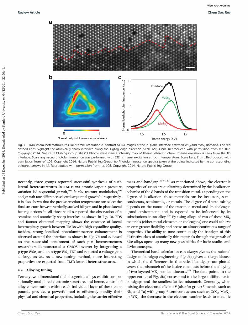
Recently, three groups reported successful synthesis of suchlateral heterosturctures in TMDs via atomic vapour pressurevariation led sequential growth,105 in situ reactant modulation,106
and growth rate difference selected sequential growth107 respectively.It is also shown that the precise reaction temperature can select thefinal structure between vertically stacked bilayers and in-plane lateralheterojunctions.107 All three studies reported the observation of aseamless and atomically sharp interface as shown in Fig. 7a. EDSand Raman elemental mapping shows the existence of lateralheteroepitaxy growth between TMDs with high crystalline quality.Besides, strong localized photoluminescence enhancement isobserved around the interface as shown in Fig. 7b and c. Basedon the successful obtainment of such p–n heterostructuresresearchers demonstrated a CMOS inverter by integrating ap-type WSe2 and an n-type WS2 FET and reported a voltage gainas large as 24. As a new tuning method, more interestingproperties are expected from TMD lateral heterostructures.
4.2 Alloying tuning
Ternary two-dimensional dichalcogenide alloys exhibit compo-sitionally modulated electronic structure, and hence, control ofalloy concentration within each individual layer of these com-pounds provides a powerful tool to efficiently modify theirphysical and chemical properties, including the carrier effective
mass and bandgap.108–111 As mentioned above, the electronicproperties of TMDs are qualitatively determined by the localizationbehavior of the d-bands of the transition metal. Depending on thedegree of localization, these materials can be insulators, semi-conductors, semimetals, or metals. The degree of d-state mixingdepends on the nature of the transition metal and its chalcogenligand environment, and is expected to be influenced by itssubstitutions in an alloy.108 By using alloys of two of these MX2
materials (either metal elements or chalcogens) one could achievean even greater flexibility and access an almost continuous range ofproperties. The ability to tune continuously the bandgap of thisdistinctive class of atomically thin materials through the growth ofS/Se alloys opens up many new possibilities for basic studies anddevice concepts.
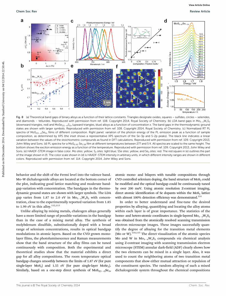
Theoretical band calculation can always give us the rationaldesign on bandgap engineering. Fig. 8(a) gives us the guidance,in which the differences in theoretical bandgaps are plottedversus the mismatch of the lattice constants before the alloyingof two layered MX2 semiconductors.108 The data points in theupper corner of Fig. 8(a) correspond to the largest difference inbandgaps and the smallest lattice mismatch. Generally, whenmixing the electron-deficient V (also for group 5 metals, such asNb, and Ta) with group 6 semiconductors such as CrX2, MoX2,or WX2, the decrease in the electron number leads to metallic
Fig. 7 TMD lateral heterostructures. (a) Atomic-resolution Z-contrast STEM images of the in-plane interface between WS2 and MoS2 domains. The reddashed lines highlight the atomically sharp interface along the zigzag-edge direction. Scale bar, 1 nm. Reproduced with permission from ref. 107.Copyright 2014, Nature Publishing Group. (b) 2D Photoluminescence intensity map of lateral heterostructure. Intense emission is seen from the 1Dinterface. Scanning micro-photoluminescence was performed with 532 nm laser excitation at room temperature. Scale bars, 2 mm. Reproduced withpermission from ref. 105. Copyright 2014, Nature Publishing Group. (c) Photoluminescence spectra taken at the points indicated by the correspondingcoloured arrows in (b). Reproduced with permission from ref. 105. Copyright 2014, Nature Publishing Group.
behavior and the shift of the Fermi level into the valence band.Mo–W dichalcogenide alloys are located at the bottom corner ofthe plot, indicating good lattice matching and moderate band-gap variation with concentration. The bandgaps in the thermo-dynamic ground states are shown with larger symbols. The LDAgap varies from 1.87 to 2.0 eV in Mo1�xWxS2 with concen-tration, close to the experimentally reported variation from 1.85to 1.99 eV in this alloy.112,113
Unlike alloying by mixing metals, chalcogen alloys generallyhave a more limited range of possible variations in the bandgapthan in the case of a mixing metal alloy. The synthesis ofmolybdenum disulfide, substitutionally doped with a broadrange of selenium concentrations, results in optical bandgapmodulations in atomic layers. Based on the CVD grown mono-layer films, the photoluminescence and Raman measurementsshow that the band structure of the alloy films can be tunedcontinuously with composition. Both the experimental andtheoretical studies show that the material exhibits a directgap for all alloy compositions. The room temperature opticalbandgap changes smoothly between the limits of 1.87 eV (for puresingle-layer MoS2) and 1.55 eV (for pure single-layer MoSe2).Similarly, based on a one-step direct synthesis of MoS2(1�x)Se2x
atomic mono- and bilayers with tunable compositions throughCVD controlled selenium doping, the band structure of MoS2 couldbe modified and the optical bandgap could be continuously tunedby over 200 meV. Using atomic resolution Z-contrast imaging,direct atomic identification of Se dopants within the MoS2 latticewith almost 100% detection efficiency was demonstrated.114
In order to better understand and fine-tune the desiredproperties by alloying, quantifying and locating the alloy atomswithin each layer is of great importance. The statistics of thehomo- and hetero-atomic coordinates in single-layered Mo1�xWxS2
was obtained from the atomically resolved scanning transmissionelectron microscope images. These images successfully quan-tify the degree of alloying for the transition metal elements(Mo or W).110,115 The direct visualization of the atomic speciesMo and W in Mo1�xWxS2 compounds via chemical analysisusing Z-contrast imaging with scanning transmission electronmicroscope (STEM) annular dark-field (ADF) clearly shows howthe two elements can be mixed in a single layer. Also, it wasused to count the neighboring atoms of two transition metalcomponents that show either mutual attraction or repulsion ofthe constituent species. The random alloying of such a mixeddichalcogenide system throughout the chemical compositions
Fig. 8 (a) Theoretical band gaps of binary alloys as a function of their lattice constants. Triangles designate oxides, squares – sulfides, circles – selenides,and diamonds – tellurides. Reproduced with permission from ref. 108. Copyright 2014, Royal Society of Chemistry. (b) LDA band gaps in Mo1�xWxS2
(downward triangles, red) and MoSe2(1�x)S2x (upward triangles, blue) alloys as a function of concentration x. The band gaps in the thermodynamic groundstates are shown with larger symbols. Reproduced with permission from ref. 108. Copyright 2014, Royal Society of Chemistry. (c) Normalized RT PLspectra of MoS2(1�x)Se2x films of different composition. Right panel: variation of the photon energy of the PL emission peak as a function of samplecomposition, as determined by XPS (the inset shows a representative XPS spectrum of the Se-3p and S-2p peaks). The black line indicates a linearvariation between the values of the stoichiometric compounds as found in DFT calculations. Reproduced with permission from ref. 109. Copyright 2013,John Wiley and Sons. (d) PL spectra for a MoS0.42 Se1.58 film at different temperatures between 277 and 5 K. All spectra are scaled to the same height. Thebottom shows the exciton emission energy as a function of the temperature. Reproduced with permission from ref. 109. Copyright 2013, John Wiley andSons. (e) HAADF-STEM image in false color. Mo sites: yellow; S2 sites: light blue; SSe sites: yellow, and Se2 sites: red. The red square in (e) outlines the partof the image shown in (f). The color scale shown in (d) is HAADF-STEM intensity in arbitrary units, in which different intensity ranges are shown in differentcolors. Reproduced with permission from ref. 114. Copyright 2014, John Wiley and Sons.
provides a direct proof of the alloying degree on individualatomic basis.
5. Gating, pressure, and lighting tuning5.1 Electric field gating effect
Electric-field control of charge carrier density has attractedmuch attention since it is remarkably simple for modulatingphysical properties of condensed matters and for exploring newfunctionalities with a transistor configuration.8,116,117 Addingcarriers to layered chalcogenides can produce remarkablecollective electronic effects owing to their enriched electronicphases, such as charge density wave and superconductivity.19
Besides the chemical doping/intercalation mentioned above,electric-field tuning of surface carrier density through carrieraccumulation or depletion in TMD-based field-effect-transistors isfree from additional structural disorder and operating in acontrollable/reversible way, especially at their monolayer limit.Therefore, to control electronic phases of layered TMDs inelectrical means is attracting growing interest not only forunderstanding the fundamental physics but also practicalelectronics and spintronics applications.118
The 2D nature of the layered TMDs and the resulting carrierquantum confinement38 decides that the layered TMDs canserve as the ideal charge transport channel for a high perfor-mance transistor. As an example, the field effect transistorsbased on a single layer MoS2 with oxide as a gate insulatorexhibit a large current on/off ratio exceeding 1 � 108 at roomtemperature8,119,120 which serve as the platform towards therealization of electronics and low-standby-power integratedcircuits based on two-dimensional materials. The presence ofthe quantum mechanical confinement and further modifica-tion of the interfacial band alignment with the external gateelectric field121 provide us with the room-temperature fieldeffect transistors with a very large on/off ratio and thus allowthe observation of a metal–insulator transition in monolayerMoS2.116 It should be addressed that the 2D nature of the TMDsresults in charge transport that is highly sensitive to a numberof factors such as substrates/dielectric,122–125 cleanliness (sur-face adsorbates),126–132 and contact metals,133–139 providing thepossibilities of the mobility enhancement/engineering withthese factors.
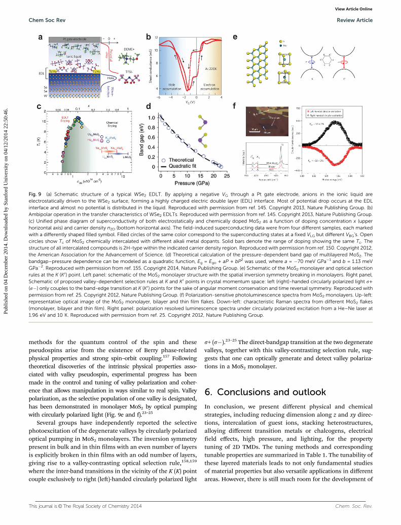
To realize novel field-effect modulated electronic phenom-ena in solids, a broad range of attainable carrier density isalways required. The power of an electric double layer transistorwith ionic liquid gating to achieve high sheet carrier densitiesbeyond the maximum attainable range of conventional oxidegate dielectrics has been recently exploited to modulate novelelectronic properties and quantum phenomena on chalco-genides.140–142 The access of field-effect induced emergentphenomena such as superconductivity, ferromagnetism andmetal–insulator transitions with EDLTs provides a powerfulway to study novel physical phenomena at such highly-chargedinterfaces.141–144 The recent application of the ionic gatingtechnique allows the achievement of the ultrathin carrier
density on MX2 surfaces and large regime tuning of the Fermilevel in the band structure. This powerful technique furtherplays a vital role in the experimental realization of the electricfield induced Zeeman polarization,23 the ambipolar operatedtransistor,145–148 and the gating induced superconductivity inMX2 systems (Fig. 9a–c).149,150
As another advantage of the transistor configuration, theintrinsic inversion symmetry can be broken simply by applyinga perpendicular electric field in bilayer or bulk two-dimensionalelectron systems where the crystal symmetry governs the natureof electronic Bloch states.145,151 For example, in bilayer MoS2
transistors, the circularly polarized photoluminescence can becontinuously tuned from �15 to 15% as a function of gatevoltage, whereas in the structurally non-centrosymmetricmonolayer MoS2 case the photoluminescence polarization isgate independent.151 The observations demonstrated the con-tinuous tuning of orbital magnetic moments between positiveand negative values through symmetry control by an electricfield. More interestingly, with the electric field induced inver-sion symmetry breaking, a spin-coupled valley photocurrentwhose direction and magnitude depend on the degree ofcircular polarization of the incident radiation can be furthergreatly modulated with an external electric field in an electric-double-layer transistor based on WSe2.152 Such room tempera-ture generation and electric control of valley/spin photocurrentprovide a new property of electrons in MX2 systems, therebyenabling new degrees of control for quantum-confined spin-tronics devices.152–154
5.2 Pressure induced insulator–metal transition
Unlike mono-atomic multilayered graphene with sp2 hybridiza-tion, multilayered MoS2 coupled with its d-orbital electronicstates and small vdW gap raises the prospects of strong S–Sinterlayer interactions under axial compression that might leadto an electronic phase transition (Fig. 9d).155 With high pres-sure experiments on exfoliated single crystalline MoS2 up to35 GPa, it was found that the pressure induced a latticedistortion involving anisotropic c/a axial compression begin-ning at B10 GPa in multilayered MoS2. This compression leadsto an intermediate state followed by a pressure-induced insu-lator–metal transition at B19 GPa. First-principle theoreticalcalculations attribute the origin of the metallic electronic statesto S–S interactions as the vdW gap closes at high pressures. Thepressure control provides a possibility for the development ofnanoscale pressure switches, sensors and multi-physics deviceswith coupled electrical, vibrational, optical and structural prop-erties using multilayered MoS2 and semiconducting TMDs.155
5.3 Valley polarization by circularly-polarized light
From the physics viewpoint, the recent emergence of transitionmetal dichalcogenides provides a new platform for exploringthe internal quantum degrees of freedom of electrons including theelectron spin, the layer pseudospin, and the valley pseudospin.156
Owing to hexagonal in-plane lattice structure, where valleys ofenergy-momentum dispersion are generally expected at the cornersof the hexagonal Brillouin zone (at the K and �K points), new
methods for the quantum control of the spin and thesepseudospins arise from the existence of Berry phase-relatedphysical properties and strong spin–orbit coupling.157 Followingtheoretical discoveries of the intrinsic physical properties asso-ciated with valley pseudospin, experimental progress has beenmade in the control and tuning of valley polarization and coher-ence that allows manipulation in ways similar to real spin. Valleypolarization, as the selective population of one valley is designated,has been demonstrated in monolayer MoS2 by optical pumpingwith circularly polarized light (Fig. 9e and f).23–25
Several groups have independently reported the selectivephotoexcitation of the degenerate valleys by circularly polarizedoptical pumping in MoS2 monolayers. The inversion symmetrypresent in bulk and in thin films with an even number of layersis explicitly broken in thin films with an odd number of layers,giving rise to a valley-contrasting optical selection rule,158,159
where the inter-band transitions in the vicinity of the K (K) pointcouple exclusively to right (left)-handed circularly polarized light
s+ (s�).23–25 The direct-bandgap transition at the two degeneratevalleys, together with this valley-contrasting selection rule, sug-gests that one can optically generate and detect valley polariza-tions in a MoS2 monolayer.
6. Conclusions and outlook
In conclusion, we present different physical and chemicalstrategies, including reducing dimension along z and xy direc-tions, intercalation of guest ions, stacking heterostructures,alloying different transition metals or chalcogens, electricalfield effects, high pressure, and lighting, for the propertytuning of 2D TMDs. The tuning methods and correspondingtunable properties are summarized in Table 1. The tunability ofthese layered materials leads to not only fundamental studiesof material properties but also versatile applications in differentareas. However, there is still much room for the development of
Fig. 9 (a) Schematic structure of a typical WSe2 EDLT. By applying a negative VG through a Pt gate electrode, anions in the ionic liquid areelectrostatically driven to the WSe2 surface, forming a highly charged electric double layer (EDL) interface. Most of potential drop occurs at the EDLinterface and almost no potential is distributed in the liquid. Reproduced with permission from ref. 145. Copyright 2013, Nature Publishing Group. (b)Ambipolar operation in the transfer characteristics of WSe2 EDLTs. Reproduced with permission from ref. 145. Copyright 2013, Nature Publishing Group.(c) Unified phase diagram of superconductivity of both electrostatically and chemically doped MoS2 as a function of doping concentration x (upperhorizontal axis) and carrier density n2D (bottom horizontal axis). The field-induced superconducting data were from four different samples, each markedwith a differently shaped filled symbol. Filled circles of the same color correspond to the superconducting states at a fixed VLG but different VBG’s. Opencircles show Tc of MoS2 chemically intercalated with different alkali metal dopants. Solid bars denote the range of doping showing the same Tc. Thestructure of all intercalated compounds is 2H-type within the indicated carrier density region. Reproduced with permission from ref. 150. Copyright 2012,the American Association for the Advancement of Science. (d) Theoretical calculation of the pressure-dependent band gap of multilayered MoS2. Thebandgap–pressure dependence can be modeled as a quadratic function, Eg = Ego + aP + bP2 was used, where a = �70 meV GPa�1 and b = 1.13 meVGPa�2. Reproduced with permission from ref. 155. Copyright 2014, Nature Publishing Group. (e) Schematic of the MoS2 monolayer and optical selectionrules at the K (K0) point. Left panel: schematic of the MoS2 monolayer structure with the spatial inversion symmetry breaking in monolayers. Right panel,Schematic of proposed valley-dependent selection rules at K and K0 points in crystal momentum space: left (right)-handed circularly polarized light s+(s�) only couples to the band-edge transition at K (K0) points for the sake of angular moment conservation and time reversal symmetry. Reproduced withpermission from ref. 25. Copyright 2012, Nature Publishing Group. (f) Polarization-sensitive photoluminescence spectra from MoS2 monolayers. Up-left:representative optical image of the MoS2 monolayer, bilayer and thin film flakes. Down-left: characteristic Raman spectra from different MoS2 flakes(monolayer, bilayer and thin film). Right panel: polarization resolved luminescence spectra under circularly polarized excitation from a He–Ne laser at1.96 eV and 10 K. Reproduced with permission from ref. 25. Copyright 2012, Nature Publishing Group.
tunable 2D TMDs. For example, the synthesis of large scale andhigh quality single layer 2D TMDs needs to be further boostedfor high performance devices; band structure and Fermi leveltuning may become powerful tools in photoelectrocatalysis;carrier density tuning has the potential for optimizing thesuperconducting temperature. A number of important andexciting studies and applications employing the tunable proper-ties of 2D TMDs will certainly come out in the near future.
Acknowledgements
We acknowledge support by the Department of Energy, Officeof Basic Energy Sciences, Materials Sciences and EngineeringDivision, under Contract DE-AC02-76-SFO0515.
References
1 K. S. Novoselov, A. K. Geim, S. V. Morozov, D. Jiang,Y. Zhang, S. V. Dubonos, I. V. Grigorieva and A. A. Firsov,Science, 2004, 306, 666–669.
2 K. S. Novoselov, D. Jiang, F. Schedin, T. J. Booth, V. V.Khotkevich, S. V. Morozov and A. K. Geim, Proc. Natl. Acad.Sci. U. S. A., 2005, 102, 10451–10453.
3 A. K. Geim and K. S. Novoselov, Nat. Mater., 2007, 6, 183–191.4 M. Xu, T. Liang, M. Shi and H. Chen, Chem. Rev., 2013, 113,
3766–3798.5 L. Ci, L. Song, C. Jin, D. Jariwala, D. Wu, Y. Li, A. Srivastava,
Z. F. Wang, K. Storr, L. Balicas, F. Liu and P. M. Ajayan,Nat. Mater., 2010, 9, 430–435.
6 Q. H. Wang, K. Kalantar-Zadeh, A. Kis, J. N. Coleman andM. S. Strano, Nat. Nano, 2012, 7, 699–712.
7 S. Z. Butler, S. M. Hollen, L. Cao, Y. Cui, J. A. Gupta,H. R. Gutierrez, T. F. Heinz, S. S. Hong, J. Huang, A. F.Ismach, E. Johnston-Halperin, M. Kuno, V. V. Plashnitsa,R. D. Robinson, R. S. Ruoff, S. Salahuddin, J. Shan, L. Shi,M. G. Spencer, M. Terrones, W. Windl and J. E. Goldberger,ACS Nano, 2013, 7, 2898–2926.
8 B. Radisavljevic, A. Radenovic, J. Brivio, V. Giacometti andA. Kis, Nat. Nano, 2011, 6, 147–150.
9 H. Zhang, C.-X. Liu, X.-L. Qi, X. Dai, Z. Fang and S.-C.Zhang, Nat. Phys., 2009, 5, 438–442.
10 Y. L. Chen, J. G. Analytis, J.-H. Chu, Z. K. Liu, S.-K. Mo,X. L. Qi, H. J. Zhang, D. H. Lu, X. Dai, Z. Fang, S. C. Zhang,
I. R. Fisher, Z. Hussain and Z.-X. Shen, Science, 2009, 325,178–181.
11 M. Chhowalla, H. S. Shin, G. Eda, L.-J. Li, K. P. Loh andH. Zhang, Nat. Chem., 2013, 5, 263–275.
12 B. Hinnemann, P. G. Moses, J. Bonde, K. P. Jørgensen,J. H. Nielsen, S. Horch, I. Chorkendorff and J. K. Nørskov,J. Am. Chem. Soc., 2005, 127, 5308–5309.
13 H. Li, J. Wu, Z. Yin and H. Zhang, Acc. Chem. Res., 2014, 47,1067–1075.
14 X. Huang, C. Tan, Z. Yin and H. Zhang, Adv. Mater., 2014,26, 2185–2204.
15 X. Huang, Z. Zeng and H. Zhang, Chem. Soc. Rev., 2013, 42,1934–1946.
16 D. Jariwala, V. K. Sangwan, L. J. Lauhon, T. J. Marks andM. C. Hersam, ACS Nano, 2014, 8, 1102–1120.
17 D. Kong, H. Wang, J. J. Cha, M. Pasta, K. J. Koski, J. Yaoand Y. Cui, Nano Lett., 2013, 13, 1341–1347.
18 M. S. Dresselhaus, Intercalation in layered materials, PlenumPress, New York, 1986.
19 J. A. Wilson and A. D. Yoffe, Adv. Phys., 1969, 18, 193–335.20 L. Mattheiss, Phys. Rev. B: Condens. Matter Mater. Phys.,
1973, 8, 3719.21 A. C. Neto, Phys. Rev. Lett., 2001, 86, 4382.22 Z. Yin, H. Li, H. Li, L. Jiang, Y. Shi, Y. Sun, G. Lu, Q. Zhang,
X. Chen and H. Zhang, ACS Nano, 2012, 6, 74–80.23 T. Cao, G. Wang, W. P. Han, H. Q. Ye, C. R. Zhu, J. R. Shi,
Q. Niu, P. H. Tan, E. Wang, B. L. Liu and J. Feng, Nat.Commun., 2012, 3, 887.
24 K. F. Mak, K. He, J. Shan and T. F. Heinz, Nat. Nano, 2012,7, 494–498.
25 H. Zeng, J. Dai, W. Yao, D. Xiao and X. Cui, Nat. Nano,2012, 7, 490–493.
26 H. J. Conley, B. Wang, J. I. Ziegler, R. F. Haglund, S. T.Pantelides and K. I. Bolotin, Nano Lett., 2013, 13, 3626–3630.
27 K.-K. Liu, W. Zhang, Y.-H. Lee, Y.-C. Lin, M.-T. Chang, C.-Y.Su, C.-S. Chang, H. Li, Y. Shi and H. Zhang, Nano Lett., 2012,12, 1538–1544.
28 H. S. Lee, S.-W. Min, Y.-G. Chang, M. K. Park, T. Nam,H. Kim, J. H. Kim, S. Ryu and S. Im, Nano Lett., 2012, 12,3695–3700.
29 Y. Shi, W. Zhou, A.-Y. Lu, W. Fang, Y.-H. Lee, A. L. Hsu,S. M. Kim, K. K. Kim, H. Y. Yang and L.-J. Li, Nano Lett.,2012, 12, 2784–2791.
30 Y. Zhan, Z. Liu, S. Najmaei, P. M. Ajayan and J. Lou, Small,2012, 8, 966–971.
32 W. Zhu, T. Low, Y.-H. Lee, H. Wang, D. B. Farmer, J. Kong,F. Xia and P. Avouris, Nat. Commun., 2014, 5, 3087.
33 J. Wu, H. Schmidt, K. K. Amara, X. Xu, G. Eda andB. Ozyilmaz, Nano Lett., 2014, 14, 2730–2734.
34 P. Joensen, R. F. Frindt and S. R. Morrison, Mater. Res.Bull., 1986, 21, 457–461.
35 Z. Zeng, Z. Yin, X. Huang, H. Li, Q. He, G. Lu, F. Boey andH. Zhang, Angew. Chem., Int. Ed., 2011, 50, 11093–11097.
Table 1 Summary of 2D TMD tuning strategies and tunable properties
Tuning strategies Tunable properties
z direction dimension Electronic band structure, optical propertyxy directions dimension Electronic band structure, catalytic activityIntercalation Thermal conductivity, super conductivity,
optical property, catalytic activityHeterostructure Electronic and optical propertiesAlloying Bandgap, carrier density and effective mass,
optical propertyGating Carrier density and mobility, optical propertyPressure Electronic propertyLighting Valley polarization
36 T. S. Li and G. L. Galli, J. Phys. Chem. C, 2007, 111, 16192–16196.37 S. Lebegue and O. Eriksson, Phys. Rev. B: Condens. Matter
Mater. Phys., 2009, 79, 115409.38 A. Splendiani, L. Sun, Y. Zhang, T. Li, J. Kim, C.-Y. Chim,
G. Galli and F. Wang, Nano Lett., 2010, 10, 1271–1275.39 K. F. Mak, C. Lee, J. Hone, J. Shan and T. F. Heinz, Phys.
Rev. Lett., 2010, 105, 136805.40 W. C. Jin, P. C. Yeh, N. Zaki, D. T. Zhang, J. T. Sadowski,
A. Al-Mahboob, A. M. van der Zande, D. A. Chenet,J. I. Dadap, I. P. Herman, P. Sutter, J. Hone andR. M. Osgood, Phys. Rev. Lett., 2013, 111, 106801.
41 Y. Zhang, T. R. Chang, B. Zhou, Y. T. Cui, H. Yan, Z. K. Liu,F. Schmitt, J. Lee, R. Moore, Y. L. Chen, H. Lin, H. T. Jeng,S. K. Mo, Z. Hussain, A. Bansil and Z. X. Shen, Nat.Nanotechnol., 2014, 9, 111–115.
42 R. Tenne, L. Margulis, M. Genut and G. Hodes, Nature,1992, 360, 444–446.
43 Y. Feldman, E. Wasserman, D. J. Srolovitz and R. Tenne,Science, 1995, 267, 222–225.
44 R. Tenne, Nat. Nano, 2006, 1, 103–111.45 M. V. Bollinger, J. V. Lauritsen, K. W. Jacobsen, J. K. Nørskov,
S. Helveg and F. Besenbacher, Phys. Rev. Lett., 2001, 87, 196803.46 J. V. Lauritsen, J. Kibsgaard, S. Helveg, H. Topsoe, B. S.
Clausen, E. Laegsgaard and F. Besenbacher, Nat. Nano,2007, 2, 53–58.
47 T. F. Jaramillo, K. P. Jørgensen, J. Bonde, J. H. Nielsen,S. Horch and I. Chorkendorff, Science, 2007, 317, 100–102.
48 X. Huang, Z. Zeng, S. Bao, M. Wang, X. Qi, Z. Fan andH. Zhang, Nat. Commun., 2013, 4, 1444.
49 Z. Zeng, C. Tan, X. Huang, S. Bao and H. Zhang, EnergyEnviron. Sci., 2014, 7, 797–803.
50 C. Tsai, K. Chan, F. Abild-Pedersen and J. K. Norskov, Phys.Chem. Chem. Phys., 2014, 16, 13156–13164.
51 H. Wang, D. Kong, P. Johanes, J. J. Cha, G. Zheng, K. Yan,N. Liu and Y. Cui, Nano Lett., 2013, 13, 3426–3433.
52 J. Bonde, P. G. Moses, T. F. Jaramillo, J. K. Norskov andI. Chorkendorff, Faraday Discuss., 2009, 140, 219–231.
53 Y. Li, H. Wang, L. Xie, Y. Liang, G. Hong and H. Dai, J. Am.Chem. Soc., 2011, 133, 7296–7299.
54 Z. Chen, D. Cummins, B. N. Reinecke, E. Clark, M. K. Sunkaraand T. F. Jaramillo, Nano Lett., 2011, 11, 4168–4175.
55 J. Kibsgaard, Z. Chen, B. N. Reinecke and T. F. Jaramillo,Nat. Mater., 2012, 11, 963–969.
56 J. Xie, H. Zhang, S. Li, R. Wang, X. Sun, M. Zhou, J. Zhou,X. W. Lou and Y. Xie, Adv. Mater., 2013, 25, 5807–5813.
57 H. I. Karunadasa, E. Montalvo, Y. Sun, M. Majda, J. R. Longand C. J. Chang, Science, 2012, 335, 698–702.
58 F. R. Gamble, J. H. Osiecki, M. Cais, R. Pisharody,F. J. DiSalvo and T. H. Geballe, Science, 1971, 174, 493–497.
59 D.-Y. Chung, T. Hogan, P. Brazis, M. Rocci-Lane, C. Kannewurf,M. Bastea, C. Uher and M. G. Kanatzidis, Science, 2000, 287,1024–1027.
60 C. Wan, Y. Wang, N. Wang, W. Norimatsu, M. Kusunokiand K. Koumoto, J. Electron. Mater., 2011, 40, 1271–1280.
61 J. Cho, M. D. Losego, H. G. Zhang, H. Kim, J. Zuo, I. Petrov,D. G. Cahill and P. V. Braun, Nat. Commun., 2014, 5, 4035.
62 E. Morosan, H. W. Zandbergen, B. S. Dennis, J. W. G. Bos,Y. Onose, T. Klimczuk, A. P. Ramirez, N. P. Ong andR. J. Cava, Nat. Phys., 2006, 2, 544–550.
63 Y. S. Hor, A. J. Williams, J. G. Checkelsky, P. Roushan,J. Seo, Q. Xu, H. W. Zandbergen, A. Yazdani, N. P. Ong andR. J. Cava, Phys. Rev. Lett., 2010, 104, 057001.
64 M. Kriener, K. Segawa, Z. Ren, S. Sasaki, S. Wada,S. Kuwabata and Y. Ando, Phys. Rev. B: Condens. MatterMater. Phys., 2011, 84, 054513.
65 J. Guo, S. Jin, G. Wang, S. Wang, K. Zhu, T. Zhou, M. Heand X. Chen, Phys. Rev. B: Condens. Matter Mater. Phys.,2010, 82, 180520.
66 M. Burrard-Lucas, D. G. Free, S. J. Sedlmaier, J. D. Wright,S. J. Cassidy, Y. Hara, A. J. Corkett, T. Lancaster, P. J. Baker,S. J. Blundell and S. J. Clarke, Nat. Mater., 2013, 12, 15–19.
67 K. J. Koski, J. J. Cha, B. W. Reed, C. D. Wessells, D. Kongand Y. Cui, J. Am. Chem. Soc., 2012, 134, 7584–7587.
68 J. Yao, K. J. Koski, W. Luo, J. J. Cha, L. Hu, D. Kong,V. K. Narasimhan, K. Huo and Y. Cui, Nat. Commun., 2014,5, 5670.
69 J. J. Cha, K. J. Koski, K. C. Y. Huang, K. X. Wang, W. Luo,D. Kong, Z. Yu, S. Fan, M. L. Brongersma and Y. Cui, NanoLett., 2013, 13, 5913–5918.
70 M. A. Py and R. R. Haering, Can. J. Phys., 1983, 61, 76–84.71 H. Wang, Z. Lu, S. Xu, D. Kong, J. J. Cha, G. Zheng, P.-C.
Hsu, K. Yan, D. Bradshaw, F. B. Prinz and Y. Cui, Proc. Natl.Acad. Sci. U. S. A., 2013, 110, 19701–19706.
72 M. A. Lukowski, A. S. Daniel, F. Meng, A. Forticaux, L. Liand S. Jin, J. Am. Chem. Soc., 2013, 135, 10274–10277.
73 D. Voiry, H. Yamaguchi, J. Li, R. Silva, D. C. B. Alves,T. Fujita, M. Chen, T. Asefa, V. B. Shenoy, G. Eda andM. Chhowalla, Nat. Mater., 2013, 12, 850–855.
74 Z. Lu, H. Wang, D. Kong, K. Yan, P.-C. Hsu, G. Zheng,H. Yao, Z. Liang, X. Sun and Y. Cui, Nat. Commun., 2014,5, 4345.
75 H. Wang, Z. Lu, D. Kong, J. Sun, T. M. Hymel and Y. Cui,ACS Nano, 2014, 8, 4940–4947.
76 D. Voiry, M. Salehi, R. Silva, T. Fujita, M. Chen, T. Asefa,V. B. Shenoy, G. Eda and M. Chhowalla, Nano Lett., 2013,13, 6222–6227.
77 M. A. Lukowski, A. S. Daniel, C. R. English, F. Meng,A. Forticaux, R. J. Hamers and S. Jin, Energy Environ. Sci.,2014, 7, 2608.
78 C. Dean, A. Young, I. Meric, C. Lee, L. Wang, S. Sorgenfrei,K. Watanabe, T. Taniguchi, P. Kim and K. Shepard, Nat.Nanotechnol., 2010, 5, 722–726.
79 T. Georgiou, R. Jalil, B. D. Belle, L. Britnell, R. V.Gorbachev, S. V. Morozov, Y.-J. Kim, A. Gholinia, S. J. Haighand O. Makarovsky, Nat. Nanotechnol., 2013, 8, 100–103.
80 J. Kang, S. Tongay, J. Zhou, J. Li and J. Wu, Appl. Phys. Lett.,2013, 102, 012111.
81 R. Cheng, D. Li, H. Zhou, C. Wang, A. Yin, S. Jiang, Y. Liu,Y. Chen, Y. Huang and X. Duan, arXiv preprint arXiv:1403.3447,2014.
82 M. M. Furchi, A. Pospischil, F. Libisch, J. Burgdorfer andT. Mueller, Nano Lett., 2014, 14, 4785–4791.
83 K. Kosmider and J. Fernandez-Rossier, Phys. Rev. B: Condens.Matter Mater. Phys., 2013, 87, 075451.
84 X. Hong, J. Kim, S.-F. Shi, Y. Zhang, C. Jin, Y. Sun, S. Tongay,J. Wu, Y. Zhang and F. Wang, Nat. Nano, 2014, 9, 682–686.
85 L. Britnell, R. Gorbachev, R. Jalil, B. Belle, F. Schedin,A. Mishchenko, T. Georgiou, M. Katsnelson, L. Eaves andS. Morozov, Science, 2012, 335, 947–950.
86 B. Sachs, L. Britnell, T. Wehling, A. Eckmann, R. Jalil,B. Belle, A. Lichtenstein, M. Katsnelson and K. Novoselov,Appl. Phys. Lett., 2013, 103, 251607.
87 J. Y. Kwak, J. Hwang, B. Calderon, H. Alsalman, N. Munoz,B. Schutter and M. G. Spencer, Nano Lett., 2014, 14, 4511.
88 S. Bertolazzi, D. Krasnozhon and A. Kis, ACS Nano, 2013, 7,3246–3252.
89 M. S. Choi, G.-H. Lee, Y.-J. Yu, D.-Y. Lee, S. H. Lee, P. Kim,J. Hone and W. J. Yoo, Nat. Commun., 2013, 4, 1624.
90 H. S. Lee, S. W. Min, M. K. Park, Y. T. Lee, P. J. Jeon,J. H. Kim, S. Ryu and S. Im, Small, 2012, 8, 3111–3115.
91 W. J. Yu, Z. Li, H. Zhou, Y. Chen, Y. Wang, Y. Huang andX. Duan, Nat. Mater., 2013, 12, 246–252.
92 K. Roy, M. Padmanabhan, S. Goswami, T. P. Sai,G. Ramalingam, S. Raghavan and A. Ghosh, Nat. Nanotechnol.,2013, 8, 826–830.
93 L. Britnell, R. Ribeiro, A. Eckmann, R. Jalil, B. Belle,A. Mishchenko, Y.-J. Kim, R. Gorbachev, T. Georgiou andS. Morozov, Science, 2013, 340, 1311–1314.
94 M. Bernardi, M. Palummo and J. C. Grossman, Nano Lett.,2013, 13, 3664–3670.
95 D. Jariwala, V. K. Sangwan, C.-C. Wu, P. L. Prabhumirashi,M. L. Geier, T. J. Marks, L. J. Lauhon and M. C. Hersam,Proc. Natl. Acad. Sci. U. S. A., 2013, 110, 18076–18080.
96 M. R. Esmaeili-Rad and S. Salahuddin, Sci. Rep., 2013,3, 2345.
97 Y. Deng, Z. Luo, N. J. Conrad, H. Liu, Y. Gong, S. Najmaei,P. M. Ajayan, J. Lou, X. Xu and P. D. Ye, ACS Nano, 2014, 8,8292–8299.
98 C.-H. Lee, G.-H. Lee, A. M. van der Zande, W. Chen, Y. Li,M. Han, X. Cui, G. Arefe, C. Nuckolls, T. F. Heinz, J. Guo,J. Hone and P. Kim, Nat. Nano, 2014, 9, 676–681.
99 A. van der Zande, J. Kunstmann, A. Chernikov, D. Chenet,Y. You, X. Zhang, P. Y. Huang, T. C. Berkelbach, L. Wangand F. Zhang, Nano Lett., 2014, 14, 3869.
100 G. W. Shim, K. Yoo, S.-B. Seo, J. Shin, D. Y. Jung, I.-S. Kang,C. W. Ahn, B. J. Cho and S.-Y. Choi, ACS Nano, 2014, 8, 6655.
101 J. S. Ross, P. Klement, A. M. Jones, N. J. Ghimire, J. Yan,D. Mandrus, T. Taniguchi, K. Watanabe, K. Kitamura andW. Yao, Nat. Nanotechnol., 2014, 9, 268–272.
102 B. W. Baugher, H. O. Churchill, Y. Yang and P. Jarillo-Herrero, Nat. Nanotechnol., 2014, 9, 262–267.
103 A. Pospischil, M. M. Furchi and T. Mueller, Nat. Nanotechnol.,2014, 9, 257.
104 M. P. Levendorf, C.-J. Kim, L. Brown, P. Y. Huang, R. W.Havener, D. A. Muller and J. Park, Nature, 2012, 488, 627–632.
105 C. Huang, S. Wu, A. M. Sanchez, J. J. P. Peters, R. Beanland,J. S. Ross, P. Rivera, W. Yao, D. H. Cobden and X. Xu, Nat.Mater., 2014, 13, 1096.
106 X. Duan, C. Wang, J. C. Shaw, R. Cheng, Y. Chen, H. Li, X. Wu,Y. Tang, Q. Zhang, A. Pan, J. Jiang, R. Yu, Y. Huang andX. Duan, Nat. Nano, 2014, DOI: 10.1038/nnano.2014.222.
107 Y. Gong, J. Lin, X. Wang, G. Shi, S. Lei, Z. Lin, X. Zou, G. Ye,R. Vajtai, B. I. Yakobson, H. Terrones, M. Terrones, B. K.Tay, J. Lou, S. T. Pantelides, Z. Liu, W. Zhou and P. M.Ajayan, Nat. Mater., 2014, 13, 1135.
108 A. Kutana, E. S. Penev and B. I. Yakobson, Nanoscale, 2014,6, 5820–5825.
109 J. Mann, Q. Ma, P. M. Odenthal, M. Isarraraz, D. Le, E. Preciado,D. Barroso, K. Yamaguchi, G. V. Palacio, A. Nguyen, T. Tran,M. Wurch, A. Nguyen, V. Klee, S. Bobek, D. Z. Sun, T. F. Heinz,T. S. Rahman, R. Kawakami and L. Bartels, Adv. Mater., 2014,26, 1399–1404.
110 Y. C. Lin, D. O. Dumcenco, H. P. Komsa, Y. Niimi, A. V.Krasheninnikov, Y. S. Huang and K. Suenaga, Adv. Mater.,2014, 26, 2857–2861.
111 I. S. Kim, V. K. Sangwan, D. Jariwala, J. D. Wood, S. Park,K.-S. Chen, F. Shi, F. Ruiz-Zepeda, A. Ponce, M. Jose-Yacaman, V. P. Dravid, T. J. Marks, M. C. Hersam andL. J. Lauhon, ACS Nano, 2014, 8, 10551–10558.
112 C. H. Ho, C. S. Wu, Y. S. Huang, P. C. Liao and K. K. Tiong,J. Phys.: Condens. Matter, 1998, 10, 9317–9328.
113 S. K. Srivastava, T. K. Mandal and B. K. Samantaray, Synth.Met., 1997, 90, 135–142.
114 Q. L. Feng, Y. M. Zhu, J. H. Hong, M. Zhang, W. J. Duan,N. N. Mao, J. X. Wu, H. Xu, F. L. Dong, F. Lin, C. H. Jin,C. M. Wang, J. Zhang and L. M. Xie, Adv. Mater., 2014, 26,2648–2653.
115 D. O. Dumcenco, H. Kobayashi, Z. Liu, Y. S. Huang andK. Suenaga, Nat. Commun., 2013, 4, 1351.
116 B. Radisavljevic and A. Kis, Nat. Mater., 2013, 12, 815–820.117 C. H. Ahn, J. M. Triscone and J. Mannhart, Nature, 2003,
424, 1015–1018.118 S. Tongay, J. Zhou, C. Ataca, J. Liu, J. S. Kang,
T. S. Matthews, L. You, J. Li, J. C. Grossman and J. Wu,Nano Lett., 2013, 13, 2831–2836.
119 M. S. Fuhrer and J. Hone, Nat. Nano, 2013, 8, 146–147.120 B. Radisavljevic and A. Kis, Nat. Nano, 2013, 8, 147–148.121 S. Kim, A. Konar, W.-S. Hwang, J. H. Lee, J. Lee, J. Yang,
C. Jung, H. Kim, J.-B. Yoo, J.-Y. Choi, Y. W. Jin, S. Y. Lee,D. Jena, W. Choi and K. Kim, Nat. Commun., 2012, 3, 1011.
122 H. Liu and P. D. Ye, IEEE Electron Device Lett., 2012, 33,546–548.
123 W. Bao, X. Cai, D. Kim, K. Sridhara and M. S. Fuhrer, Appl.Phys. Lett., 2013, 102, 042104.
124 Z.-Y. Ong and M. V. Fischetti, Phys. Rev. B: Condens. MatterMater. Phys., 2013, 88, 165316.
125 L. Zeng, Z. Xin, S. Chen, G. Du, J. Kang and X. Liu, Appl.Phys. Lett., 2013, 103, 113505.
126 M. M. Perera, M.-W. Lin, H.-J. Chuang, B. P. Chamlagain,C. Wang, X. Tan, M. M.-C. Cheng, D. Tomanek andZ. Zhou, ACS Nano, 2013, 7, 4449–4458.
127 D. Jariwala, V. K. Sangwan, D. J. Late, J. E. Johns,V. P. Dravid, T. J. Marks, L. J. Lauhon and M. C. Hersam,Appl. Phys. Lett., 2013, 102, 173107.
128 V. K. Sangwan, H. N. Arnold, D. Jariwala, T. J. Marks,L. J. Lauhon and M. C. Hersam, Nano Lett., 2013, 13,4351–4355.
129 L. Ming-Wei, L. Lezhang, L. Qing, T. Xuebin, S. D. Kulwinder,Z. Peng, M. N. Vaman, C. Mark Ming-Cheng and Z. Zhixian,J. Phys. D: Appl. Phys., 2012, 45, 345102.
130 Y. Li, C.-Y. Xu, P. Hu and L. Zhen, ACS Nano, 2013, 7,7795–7804.
131 S.-L. Li, K. Wakabayashi, Y. Xu, S. Nakaharai, K. Komatsu,W.-W. Li, Y.-F. Lin, A. Aparecido-Ferreira and K. Tsukagoshi,Nano Lett., 2013, 13, 3546–3552.
132 H. Fang, M. Tosun, G. Seol, T. C. Chang, K. Takei, J. Guoand A. Javey, Nano Lett., 2013, 13, 1991–1995.
133 S. Das, H.-Y. Chen, A. V. Penumatcha and J. Appenzeller,Nano Lett., 2012, 13, 100–105.
134 I. Popov, G. Seifert and D. Tomanek, Phys. Rev. Lett., 2012,108, 156802.
135 W. Liu, J. Kang, D. Sarkar, Y. Khatami, D. Jena andK. Banerjee, Nano Lett., 2013, 13, 1983–1990.
136 S. Walia, S. Balendhran, Y. Wang, R. Ab Kadir, A. SabirinZoolfakar, P. Atkin, J. Zhen Ou, S. Sriram, K. Kalantar-zadeh and M. Bhaskaran, Appl. Phys. Lett., 2013,103, 232105.
137 C. Gong, C. Huang, J. Miller, L. Cheng, Y. Hao, D. Cobden,J. Kim, R. S. Ruoff, R. M. Wallace, K. Cho, X. Xu andY. J. Chabal, ACS Nano, 2013, 7, 11350–11357.
138 J.-R. Chen, P. M. Odenthal, A. G. Swartz, G. C. Floyd,H. Wen, K. Y. Luo and R. K. Kawakami, Nano Lett., 2013,13, 3106–3110.
139 H. Fang, S. Chuang, T. C. Chang, K. Takei, T. Takahashiand A. Javey, Nano Lett., 2012, 12, 3788–3792.
140 K. Ueno, S. Nakamura, H. Shimotani, A. Ohtomo, N. Kimura,T. Nojima, H. Aoki, Y. Iwasa and M. Kawasaki, Nat. Mater.,2008, 7, 855–858.
141 H. T. Yuan, H. Shimotani, A. Tsukazaki, A. Ohtomo,M. Kawasaki and Y. Iwasa, Adv. Funct. Mater., 2009, 19,1046–1053.
142 K. Ueno, S. Nakamura, H. Shimotani, H. T. Yuan,N. Kimura, T. Nojima, H. Aoki, Y. Iwasa and M. Kawasaki,Nat. Nanotechnol., 2011, 6, 408–412.
143 Y. Yamada, K. Ueno, T. Fukumura, H. T. Yuan,H. Shimotani, Y. Iwasa, L. Gu, S. Tsukimoto, Y. Ikuharaand M. Kawasaki, Science, 2011, 332, 1065–1067.
144 S. Asanuma, P. H. Xiang, H. Yamada, H. Sato, I. H. Inoue,H. Akoh, A. Sawa, K. Ueno, H. Shimotani, H. Yuan,M. Kawasaki and Y. Iwasa, Appl. Phys. Lett., 2010, 97, 142110.
145 H. T. Yuan, M. S. Bahramy, K. Morimoto, S. F. Wu,K. Nomura, B. J. Yang, H. Shimotani, R. Suzuki, M. Toh,C. Kloc, X. D. Xu, R. Arita, N. Nagaosa and Y. Iwasa, Nat.Phys., 2013, 9, 563–569.
146 Y. J. Zhang, J. T. Ye, Y. Matsuhashi and Y. Iwasa, Nano Lett.,2012, 12, 1136–1140.
147 Y. J. Zhang, J. T. Ye, Y. Yornogida, T. Takenobu andY. Iwasa, Nano Lett., 2013, 13, 3023–3028.
148 D. Braga, I. Gutierrez Lezama, H. Berger and A. F. Morpurgo,Nano Lett., 2012, 12, 5218–5223.
149 K. Ueno, H. Shimotani, H. T. Yuan, J. T. Ye, M. Kawasakiand Y. Iwasa, J. Phys. Soc. Jpn., 2014, 83.
150 J. T. Ye, Y. J. Zhang, R. Akashi, M. S. Bahramy, R. Arita andY. Iwasa, Science, 2012, 338, 1193–1196.
151 S. F. Wu, J. S. Ross, G. B. Liu, G. Aivazian, A. Jones,Z. Y. Fei, W. G. Zhu, D. Xiao, W. Yao, D. Cobden andX. D. Xu, Nat. Phys., 2013, 9, 149–153.
152 H. Yuan, X. Wang, B. Lian, H. Zhang, X. Fang, B. Shen,G. Xu, Y. Xu, S.-C. Zhang, H. Y. Hwang and Y. Cui, Nat.Nano, 2014, 9, 851–857.
153 S. Tarasenko, Nat. Nanotechnol., 2014, 9, 752–753.154 H. Yu, Y. Wu, G.-B. Liu, X. Xu and W. Yao, Phys. Rev. Lett.,
2014, 113, 156603.155 A. P. Nayak, S. Bhattacharyya, J. Zhu, J. Liu, X. Wu,
T. Pandey, C. Q. Jin, A. K. Singh, D. Akinwande andJ. F. Lin, Nat. Commun., 2014, 5.
156 X. D. Xu, W. Yao, D. Xiao and T. F. Heinz, Nat. Phys., 2014,10, 343–350.
157 W. Yao, D. Xiao and Q. Niu, Phys. Rev. B: Condens. MatterMater. Phys., 2008, 77, 235406.
158 D. Xiao, G. B. Liu, W. X. Feng, X. D. Xu and W. Yao, Phys.Rev. Lett., 2012, 108, 196802.


![Lithium Electrochemical Tuning for Electrocatalysis€¦ · the interlayer of materials,[12] such as layered transition metal dichalcogenides (e.g., MoS 2) and lithium transition](https://static.documents.pub/doc/80x56/6061bb8d1b6ca92a3150bd5c/lithium-electrochemical-tuning-for-electrocatalysis-the-interlayer-of-materials12.jpg)


