Diamond - Based Acoustic Devices Vincent Mortet , Oliver Williams and Ken Haenen Hasselt University, Institute for Materials Research (IMO), Wetenschapspark 1, B - 3590 Diepenbeek, Belgium IMEC vzw, Division IMOMEC, Wetenschapspark 1, B - 3590 Diepenbeek, Belgium
The genesis of acoustic wave devices comes at the end of the nineteenth century with the discovery of piezoelectricity [1] and the proof of elastic vibrations at the surface of solid materials [2] . The fi rst application of piezoelectricity was to emit and receive acoustic waves under water (SONAR). Later on, piezoelectric materials have been used as oscillators in radio transmission (quartz crystals). In the 1960s, the major discovery of interdigital transducers [3] lead to the development of surface acoustic wave devices ( SAW ). Nowadays, SAW fi lters are widely used in radiofrequency applications with operating frequencies up to the gigahertz range.
Acoustic waves are highly sensitive to small perturbations; hence, acoustic devices can be operated as sensors. The fi rst acoustic sensor was the so - called quartz crystal microbalance ( QCM ). QCMs were analyzed and improved by a suc-cession of workers starting in the 1950s. They consist of a quartz crystal, initially made to stabilize the frequencies of radio transmitters, coated with a sorptive fi lm. The next important step in acoustic sensors was made in the late 1970s when Wohltjen and Dessy made a chemical vapor sensor using a surface acoustic wave delay line [4] . More recently, acoustic plate mode ( APM ) and fl exural plate wave ( FPW ) sensors were introduced. They employ similar principles, but exploit dif-ferent acoustic propagation modes. In the last decade, two new types of acoustic devices have been developed for sensing applications: fi lm bulk acoustic resona-tors ( FBARs ) and microcantilevers ( MCs ). FBARs were fi rst developed for signal treatment, while MCs were fi rst developed for scanning probe microscopy ( SPM ).
Despite the fact that diamond is not piezoelectric, diamond has an important role to play in the development of composite acoustic devices because of its outstanding mechanical properties. The fi rst successful acoustic application of
178 7 Diamond-Based Acoustic Devices
diamond was in the fi eld of surface acoustic wave (SAW) fi lters. With the develop-ment of biotechnologies, many researchers have been working on diamond for sensor applications [5 – 7] due to diamond ’ s chemical stability and bio - inertness. Thus, the combination of diamond properties and the high sensitivity of acoustic sensors is very appealing.
In this chapter, we will fi rst consider the interest of diamond layers for acoustic applications. Then, we are going discuss the progress that has been made in R & D on diamond - based SAW fi lters. We will also review and compare the different types of acoustic devices and sensors. We will present the latest results on the development of composite acoustic sensors based on diamond.
7.2 Diamond Layers
Diamond is highly attractive for many different types of composite acoustic devices because of its mechanical properties. Diamond ’ s extreme values of hardness, Young ’ s modulus (E), stiffness and fracture strength ( σ f ) make it suitable for fl ex-ural plate wave (FPW) sensors and microcantilever (MC) sensors. Those values surpass those of Si, Si 3 N 4 and SiC [11] (see Table 7.1 ) which are commonly used for MEMS and sensors applications. The large sound velocity and high thermal conductivity of diamond have opened up possibilities to produce SAW fi lters operating in the GHz range since the operating frequency of SAW fi lters is proportional to the acoustic wave velocity. The extreme chemical stability and bio - inertness [12] of diamond make it an ideal material for sensors operating in harsh or biologic environments. Most signifi cantly, the surface of diamond is particularly stable when functionalized with biomolecules [13] . This makes diamond of par-ticular interest for biosensing applications.
Not withstanding diamond ’ s exciting properties, diamond layers suffer in general from a high surface roughness due to van der Drift growth regime of CVD diamond. Both the grain size and roughness of CVD diamond layers increase with the fi lm thickness [14] . Root mean square ( RMS ) roughness is in the range of 15 to 40 nm for a 1 µ m thick fi lm [15, 16] and several micrometers roughness is usual
Table 7.1 Stiffness and fracture strength of different materials compared to CVD diamond.
for thick ( > 100 µ m) polycrystalline CVD diamond fi lms [14, 15] . Surfaces for acoustic applications must be fl at to prevent wave scattering and propagation losses. Surface roughness must also be compatible with the photolithographic pattern resolution and deposition of piezoelectric thin fi lms.
Several approaches have been successfully used to obtain fl at diamond surfaces. Despite its extreme diffi culty, diamond polishing has been the primary method. It leads to smooth and large polycrystalline diamond wafers. Bi et al. [17] have used nanocrystalline diamond ( NCD ) fi lms with RMS roughness of 50 nm, while Mortet et al. [18] have used the fl at nucleation side of thick freestanding diamond layer grown on silicon substrates. The roughness varies with the nucleation process, that is 30 to 50 nm between 30 to 50 nm for mechanical nucleation and ∼ 10 nm for bias enhanced nucleation.
Growth of uniform and pinhole - free thin diamond layers, necessary for FPW, MCs, and MEMS applications, is not easy due to the diamond nucleation mecha-nism on foreign substrates. Nucleation density is a key parameter to control the uniformity and the roughness of thin diamond fi lms. Diamond nucleates and grows as individual grains until they coalesce to form a continuous fi lm. Thus, the fi lm ’ s coalescence thickness depends on the nucleation density. Thin coalesced fi lms with small grains size are obtained together with a high nucleation density [19, 20] . Sub - micron thick diamond membranes of ∼ 10 mm diameter have been produced by increasing the diamond nucleation density above 10 10 cm − 2 [21] . NCD fi lms grow in the van der Drift regime, its grain size and hence roughness increase with fi lm thickness. Above 1 µ m thickness, NCD fi lms become microcrystalline. Ultra - nanocrystalline diamond ( UNCD ) is of particular interest for acoustic appli-cations compared to nanocrystalline diamond. UNCD consists of a fi ne grain (3 – 5 nm) material grown with a high renucleation rate and a low surface rough-ness [22, 23] independent of fi lm thickness.
High stiffness and tensile stress are needed in order to avoid any mechanical in - plane and out - of - plane distortion of acoustic devices. Aikawa et al. [8] have shown that smaller grain sizes and high phase purity, which depends on the substrate pretreatment conditions and the deposition parameters, are required to obtain membranes with high fracture strength. Furthermore, diamond fi lms often contain large residual stress, thus a tight temperature control of the whole sub-strate is needed during the deposition.
7.3 Acoustic Sensors
Electrochemical, optical and acoustic wave sensing devices have emerged as some of the most promising biochemical sensor technologies. Together with the devel-opment of these technologies, many researchers have been working on diamond for sensor applications due to its chemical stability and bio - inertness.
Acoustic sensors operate by detecting changes in the resonant response. They are highly sensitive. They are sensitive to variations of mechanical stress,
180 7 Diamond-Based Acoustic Devices
temperature, damping and mass loading. Acoustic sensors have already been used to study physical, chemical and biological properties of gases and liquids for decades.
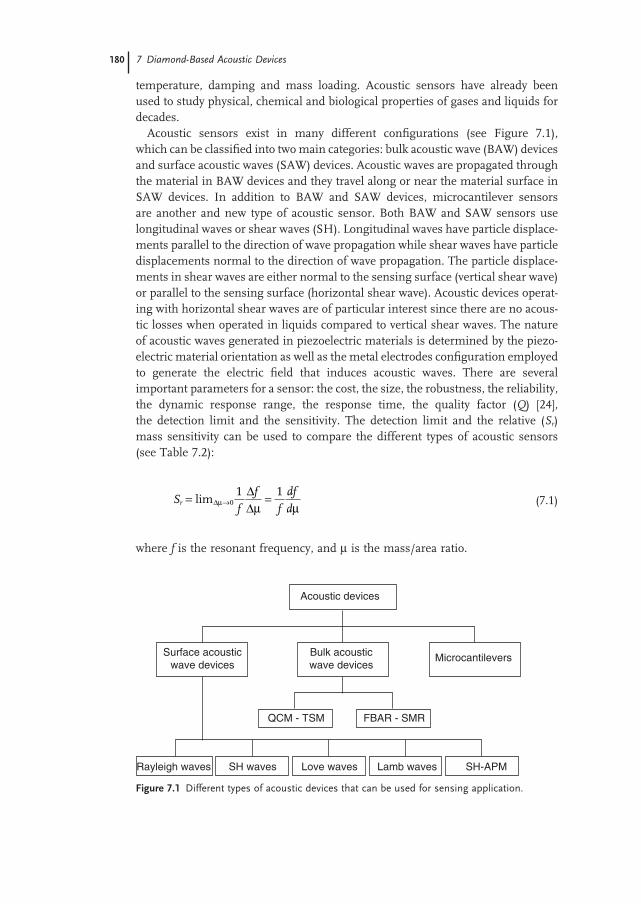
Acoustic sensors exist in many different confi gurations (see Figure 7.1 ), which can be classifi ed into two main categories: bulk acoustic wave ( BAW ) devices and surface acoustic waves (SAW) devices. Acoustic waves are propagated through the material in BAW devices and they travel along or near the material surface in SAW devices. In addition to BAW and SAW devices, microcantilever sensors are another and new type of acoustic sensor. Both BAW and SAW sensors use longitudinal waves or shear waves ( SH ). Longitudinal waves have particle displace-ments parallel to the direction of wave propagation while shear waves have particle displacements normal to the direction of wave propagation. The particle displace-ments in shear waves are either normal to the sensing surface (vertical shear wave) or parallel to the sensing surface (horizontal shear wave). Acoustic devices operat-ing with horizontal shear waves are of particular interest since there are no acous-tic losses when operated in liquids compared to vertical shear waves. The nature of acoustic waves generated in piezoelectric materials is determined by the piezo-electric material orientation as well as the metal electrodes confi guration employed to generate the electric fi eld that induces acoustic waves. There are several important parameters for a sensor: the cost, the size, the robustness, the reliability, the dynamic response range, the response time, the quality factor ( Q ) [24] , the detection limit and the sensitivity. The detection limit and the relative ( S r ) mass sensitivity can be used to compare the different types of acoustic sensors (see Table 7.2 ):
Sf
f
f
df
dr = =→lim∆
∆∆µ µ µ0
1 1 (7.1)
where f is the resonant frequency, and µ is the mass/area ratio.
Figure 7.1 Different types of acoustic devices that can be used for sensing application.
Acoustic devices
Bulk acousticwave devices
Microcantilevers
QCM - TSM
Rayleigh waves SH waves Love waves Lamb waves SH-APM
FBAR - SMR
Surface acousticwave devices
7.3 Acoustic Sensors 181
7.3.1 Bulk Acoustic Wave Sensors
7.3.1.1 Quartz Crystal Microbalance In 1959, Sauerbrey was the fi rst to relate resonant frequency change of a piezo-electric quartz crystal to mass attachment at its surface, establishing the quartz crystal microbalance ( QCM ). QCMs are a particular case of thickness shear mode ( TSM ) resonators using quartz. QCMs are typically a few hundred micrometers thick and ∼ 10 mm in diameter with a fundamental resonant frequency in the 3 – 30 MHz range. Either shear or longitudinal waves are excited by an AC voltage applied to the electrodes placed on the two sides of the quartz crystal (see Figure 7.2 ), depending on the crystal cut. The fundamental resonant frequency (f 0 ) is determined by the thickness of the piezoelectric material and its acoustic wave velocity (Equation 7.1 ). The relative sensitivity (S r ) is in inverse proportion with the sensor thickness (Equation 7.2 ):
fv
h0
02= (7.2)
Sf
v hr
p p
= − ⋅⋅
= −⋅
2 10
0ρ ρ (7.3)
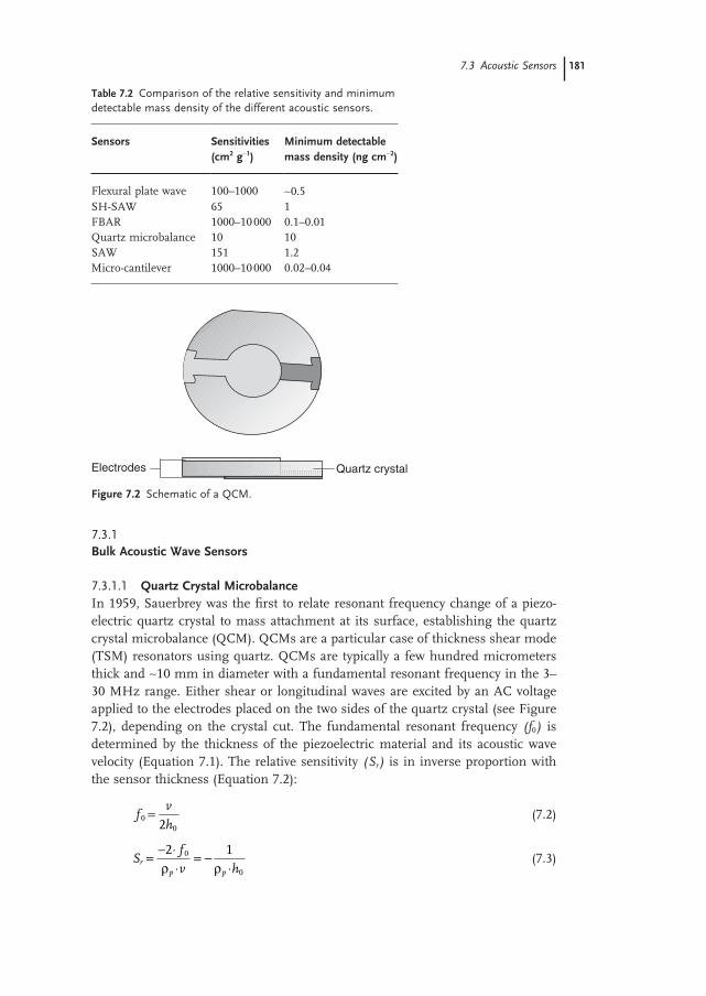
Table 7.2 Comparison of the relative sensitivity and minimum detectable mass density of the different acoustic sensors.
with v , the sound velocity (longitudinal or shear); h 0 , the quartz crystal thickness and ρ p , the piezoelectric material density.
Quartz crystal microbalance sensors are simple to use and robust, but their resonant frequency is limited by the mechanical thinning process. They have a low relative sensitivity ∼ 70 cm 2 /g compared to others acoustic sensors with a mass resolution ∼ 10 ng/cm 2 at a fundamental resonant frequency.
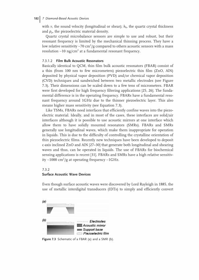
7.3.1.2 Film Bulk Acoustic Resonators Basically identical to QCM, thin fi lm bulk acoustic resonators ( FBAR ) consist of a thin (from 100 nm to few micrometers) piezoelectric thin fi lm (ZnO, AlN ) deposited by physical vapor deposition (PVD) and/or chemical vapor deposition (CVD) techniques and sandwiched between two metallic electrodes (see Figure 7.3 ). Their dimensions can be scaled down to a few tens of micrometers. FBAR were fi rst developed for high frequency fi ltering applications [25, 26] . The funda-mental difference is in the operating frequency. FBARs have a fundamental reso-nant frequency around 1GHz due to the thinner piezoelectric layer. This also means higher mass sensitivity (see Equation 7.3 ).
Like TSMs , FBARs need interfaces that effi ciently confi ne waves into the piezo-electric material. Ideally, and in most of the cases, these interfaces are solid/air interfaces although it is possible to use acoustic mirrors at one interface which allow them to have solidly mounted resonators ( SMRs ). FBARs and SMRs generally use longitudinal waves, which make them inappropriate for operation in liquids. This is due to the diffi culty of controlling the crystalline orientation of thin piezoelectric fi lms. Recently new techniques have been developed to deposit c - axis inclined ZnO and AlN [27 – 30] that generate both longitudinal and shearing waves and thus, can be operated in liquids. The use of FBARs for biochemical sensing applications is recent [31] . FBARs and SMRs have a high relative sensitiv-ity ∼ 1000 cm 2 /g at operating frequency ∼ 1GHz.
7.3.2 Surface Acoustic Wave Devices
Even though surface acoustic waves were discovered by Lord Rayleigh in 1885, the use of metallic interdigital transducers ( IDTs ) to simply and effi ciently convert
Figure 7.3 Schematic of a FBAR (a) and a SMR (b).
7.3 Acoustic Sensors 183
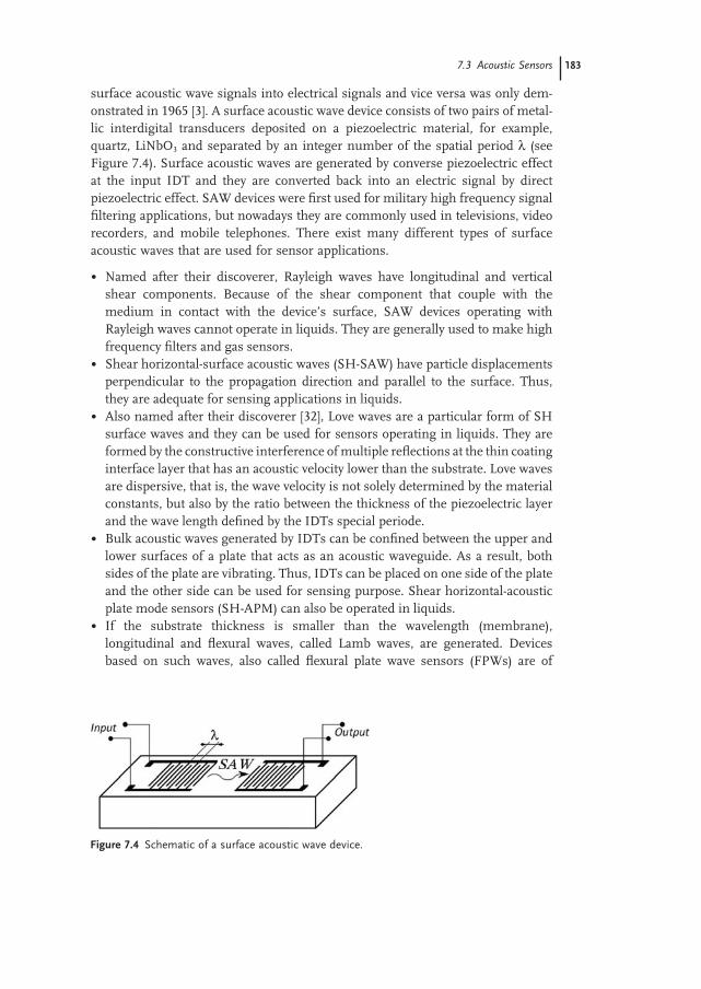
surface acoustic wave signals into electrical signals and vice versa was only dem-onstrated in 1965 [3] . A surface acoustic wave device consists of two pairs of metal-lic interdigital transducers deposited on a piezoelectric material, for example, quartz, LiNbO 3 and separated by an integer number of the spatial period λ (see Figure 7.4 ). Surface acoustic waves are generated by converse piezoelectric effect at the input IDT and they are converted back into an electric signal by direct piezoelectric effect. SAW devices were fi rst used for military high frequency signal fi ltering applications, but nowadays they are commonly used in televisions, video recorders, and mobile telephones. There exist many different types of surface acoustic waves that are used for sensor applications.
• Named after their discoverer, Rayleigh waves have longitudinal and vertical shear components. Because of the shear component that couple with the medium in contact with the device ’ s surface, SAW devices operating with Rayleigh waves cannot operate in liquids. They are generally used to make high frequency fi lters and gas sensors.
• Shear horizontal - surface acoustic waves ( SH - SAW ) have particle displacements perpendicular to the propagation direction and parallel to the surface. Thus, they are adequate for sensing applications in liquids.
• Also named after their discoverer [32] , Love waves are a particular form of SH surface waves and they can be used for sensors operating in liquids. They are formed by the constructive interference of multiple refl ections at the thin coating interface layer that has an acoustic velocity lower than the substrate. Love waves are dispersive, that is, the wave velocity is not solely determined by the material constants, but also by the ratio between the thickness of the piezoelectric layer and the wave length defi ned by the IDTs special periode.
• Bulk acoustic waves generated by IDTs can be confi ned between the upper and lower surfaces of a plate that acts as an acoustic waveguide. As a result, both sides of the plate are vibrating. Thus, IDTs can be placed on one side of the plate and the other side can be used for sensing purpose. Shear horizontal - acoustic plate mode sensors ( SH - APM ) can also be operated in liquids.
• If the substrate thickness is smaller than the wavelength (membrane), longitudinal and fl exural waves, called Lamb waves, are generated. Devices based on such waves, also called fl exural plate wave sensors ( FPWs ) are of
Figure 7.4 Schematic of a surface acoustic wave device.
184 7 Diamond-Based Acoustic Devices
special interest since they are more sensitive than other SAW sensors, and they can be operated in liquids. Their sensitivity is inversely proportional to density ( ρ ) and the thickness (t) of the membrane: S r = − 2/ ρ .t.
7.3.3 Microcantilevers
Microcantilevers are mainly used in atomic force microscopy ( AFM ). They are use to transduce minute forces (from 1 nN up to 10 µ N) that interact with a sharp tip at the cantilever ’ s free end. The interest in microfabricated cantilevers has grown with the development of the atomic force microscope. MCs are simple mechanical devices. Micromachined cantilevers are extremely sensitive, miniature, mass pro-duced, and cheap. Most microcantilevers are made of silicon. They are tiny plates of leaf spring, typically 0.2 – 1 µ m thick, 10 – 100 µ m wide and 100 – 500 µ m long, which are connected at one end to an appropriate support for convenient handling. Their fi rst use as sensor was reported in 1994 [33] . They operate either in static bending mode or in dynamic mode where the resonant frequencies of the canti-lever are monitored. While there exist many different types of excitation (electro-static, piezoelectric, resistive or optical heating, magnetic) and detection methods (capacitive, piezoresistive, magnetic) when operated in dynamic mode, the defl ec-tion of the cantilever is generally monitored using an optical lever. In this tech-nique, visible light from a low power laser refl ected on the free apex of the cantilever is displaced as the cantilever bends. This displacement is converted into an electronic signal by projecting the refl ected laser beam onto a position sensitive photodetector. Microcantilevers are sensitive to external forces, temperature, damping, and mass loading. The relative sensitivity (S r ) of a microcantilever is shown in Equation 7.4 :
St
r =⋅1
ρ (7.4)
where ρ is the density of the cantilever material and t is the cantilever thickness. Microcantilevers have a relative sensitivity ∼ 1000 cm 2 /g at an operating frequency of few a tens to hundred kilohertz.
Except for microcantilever sensors, which have been recently developed, all the described acoustic devices have proven to be excellent gravimetric sensors. The use of diamond for these devices is new and appealing because of the excellent mechanical properties of diamond. The recent progress in diamond growth allows researchers to integrate diamond in the acoustic sensors fi eld. FPW sensors, FBARs, and MCs seem particularly promising sensors due to their high sensitivity. FPW devices are particularly promising since they operate in liquids. FBARs and MCs are miniature and compatible with the inte-grated circuit technology. Composite FBAR operation in liquids has already been demonstrated [34] .
7.4 Diamond Acoustic Devices
7.4.1 Surface Acoustic Wave Devices
Surface acoustic wave (SAW) fi lters are used in a wide range of applications such as keyless entry devices, radio frequency modems and telemetry systems, alarm systems, and so on. The increasing volume of information and communication media has produced a growing demand for high performance surface acoustic wave (SAW) devices, operating in the GHz frequency range. In fi ltering applica-tions, the electrical signal to be fi ltered is converted to an acoustic signal at the fi rst interdigital transducer (IDT) by the converse piezoelectric effect and is recon-verted to an electrical signal at the second IDT by the direct piezoelectric effect. Filtering is performed during these conversions and it is directly related to the geometry of the IDTs and the mechanical and piezoelectric properties of the piezoelectric material. The operating frequency (f) of SAW devices is proportional to the acoustic wave velocity and inversely proportional to wavelength ( λ ), which is equal to the period of interdigital transducers, as shown in Equation 7.5 .
fv=λ
(7.5)
The operating frequencies of SAW fi lters based on standard piezoelectric materi-als remain under 1GHz due the limitation of optical photolithography resolution. There are several approaches to achieving higher operation frequencies on SAW fi lters: (i) to reduce the wavelength, that is, the period of IDTs, (ii) to use substrates with higher propagation velocity, or (iii) to use different propagation modes with high propagation velocities, for example, leaky waves [35] . The most attractive approach is to use substrates with high propagation velocities such as silicon, sapphire, SiC or diamond. Diamond is the most suitable material for acoustic parts because of its highest acoustic wave velocities (see Table 7.3 ). But these materials are not piezoelectric and thus they must be combined with piezoelectric fi lms.
The use of diamond in surface acoustic wave fi lters has been studied after the discovery and the development of CVD method to grow diamond. Several piezo-electric materials (KNbO 3 [36] , ZnO [17, 37 – 39] , PZT, LiTaO 3 [39] , LiNbO 3 [39] , AlN [40, 41] ) in combination with diamond substrates and structures, including SiO 2 and shorting metal layers have been investigated theoretically and experimen-tally. Theoretical calculation of the different Rayleigh wave propagation modes is diffi cult due to the multilayer structure. The problem is overcome by numerical calculation methods. Diamond - based SAW devices are dispersive, that is, the wave velocity is not solely determined by the material constants but also by the ratio between the thickness of the piezoelectric layer and the wave length defi ned by the IDTs. For the ZnO/diamond structure, wave velocities from 6400 to
7.4 Diamond Acoustic Devices 185
186 7 Diamond-Based Acoustic Devices
10 800 m s − 1 and electromechanical coupling coeffi cient K 2 from 3 to 7% were calculated. Wave velocity of 11 090 m s − 1 and K 2 of 1.4% were calculated for the AlN/diamond structure. The LiNbO 3 /diamond structure is very attractive since it is theoretically possible to obtain waves velocities of 12 000 m s − 1 and a K 2 of 9% but it also suffers from the high temperature coeffi cient of frequency ( TCF ) of LiNbO 3 , that is, the drift of the central frequency with temperature variation. The SAW velocities of these structures are twice as large as those of conventional SAW materials (see Table 7.3 ) and their K 2 values are large enough for practical applications [42] .
The most intensively and experimentally studied structure is the ZnO/diamond structure. This is probably due to the relative ease to deposit these materials with good piezoelectric properties, usually by sputtering techniques. The use of a SiO 2 layer was introduced to reduce/cancel the temperature coeffi cient of frequency (TCF) of the ZnO/diamond SAW fi lters. Since the 1990s, Sumitomo Electronic Ltd has developed and commercialized ZnO/diamond SAW fi lters with an operating frequency from 1.8 GHz to 3.8 GHz, on polished CVD diamond fi lms. These fi lters operate on the second Sezawa mode with λ = 4 µ m, have a high electromechanical coupling coeffi cient K 2 = 1.1%, a high phase velocity v = 9500 m/s, low insertion loss (7 – 9 dB) with 50 dB rejection, zero temperature deviation and a quality factor Q ∼ 630 – 750 (Sezawa wave: second acoustic mode of the Rayleigh type in layered solid structures). The power durability of ZnO/diamond SAW fi lters and LiTaO 3 SAW fi lters has been compared. Diamond SAW fi lters have superior high power durability at even 3.5 times higher frequency [43] .
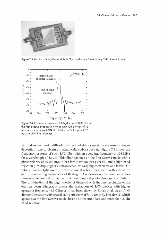
AlN/diamond SAW fi lters have also been experimentally studied by different authors [18, 44] . Compared to ZnO/diamond structrure, AlN/diamond structure has higher phase velocities, from 6000 to 12 000 m/s. Mortet et al. have used the fl at nucleation side of a thick freestanding polycrystalline CVD diamond to study AlN/diamond SAW fi lters (see Figure 7.5 ). This method presents the advantage
Table 7.3 Longitudinal acoustic wave velocity: V L = ( C 11/ ρ )1/2 and transversal acoustic wave velocity: V T = ( C 44/ ρ ) 1/2 sound velocities along the (100) direction in different materials.
Materials V L (km/s) V T (km/s)
Diamond 17.52 12.82 Cubic boron nitride 15.4 11.8 4H - SiC and 6H - SiC 12.5 7.1 3C - SiC 9.5 4.1 Silicon 8.43 5.84 AT cut quartz 5.96 3.31 PZT 4.5 2.2 AlN 11.37 6.09 ZnO 6.33 2.88
that it does not need a diffi cult diamond polishing step at the expenses of longer deposition time to obtain a mechanically stable substrate. Figure 7.6 shows the frequency response of such SAW fi lter with an operating frequency at 326 MHz for a wavelength of 32 µ m. This fi lter operates on the fi rst Sezawa mode with a phase velocity of 10 400 m/s, it has low insertion loss ( < 20 dB) and a high band rejection ( ∼ 25 dB). Higher electromechanical coupling coeffi cients and lower TCF values than ZnO/diamond structures have also been measured on this structure [45] . The operating frequencies of Rayleigh SAW devices on diamond substrates remain under 2 – 3 GHz due the limitation of optical photolithography resolution. The combination of the high velocity of diamond with the fi ne resolution of the electron beam lithography allows the realization of SAW devices with higher operating frequency (4.6 GHz) as it has been shown by Kirsch et al. on an AlN/diamond structure with spatial IDT periodicity of λ = 2 µ m [46] . This device, which operates at the fi rst Sezawa mode, has 34 dB insertion loss and more than 20 dB band rejection.
Figure 7.5 Picture of AlN/diamond SAW fi lter made on a freestanding CVD diamond layer.
Figure 7.6 Frequency response of AlN/diamond SAW fi lter at the fi rst Sezawa propagation mode with IDT periode of 32 mm and a normalized AlN fi lm thickness 2 π . h AlN / λ = 1.92, h AlN : the AlN fi lm thickness.
260 280 300 320 340 360 380-70
-60
-50
-40
-30
-20
-10
0
f0=326MHz
Out-of-band rejection
Insertion Lossat center frequency
S21
(dB
)
Frequency (MHz)
7.4 Diamond Acoustic Devices 187
188 7 Diamond-Based Acoustic Devices
On the other hand, Benetti et al. have studied the propagation of a pseudo - surface - acoustic - wave on AlN/diamond. They reported a high value of phase velocity (16 000 m/s) operating at ∼ 2 GHz, using an IDT with a line width resolution of 2 µ m. However this device suffers from high insertion loss [47] .
Insertion losses are the sum propagation loss and the IDT bidirectional loss. The bidirectional loss can be reduced using unidirectional IDTs. The contribution of the diamond substrate to propagation loss has been studied as a function of the diamond grain size by Fujii et al [48] . Smaller grain size, narrower grain distribu-tion, and preferential grain orientation reduce the propagation loss of SAW on polycrystalline diamond fi lms without infl uencing the TCF, K 2 and phase velocity of the devices [48, 49] . These results are consistent with the results of Elmasria et al. who observed that the propagation losses on the nucleation side of freestand-ing CVD diamond are three times lower in the case of bias enhanced nucleation compared to mechanically seed layers [50] , since bias enhanced nucleation leads to high nucleation density, smaller grain size and lower surface roughness without the need of a polishing step.
Despite the interest in using diamond, there is, to our knowledge, little research on SAW sensors using diamond substrates. Benetti et al. have reported that AlN/diamond SAW fi lters can operate as CO and ethanol sensors in the gas phase using Co - tetra - phenyl - porphyrin as sorptive fi lm [51] . This fact might be due to the fact that SAW devices based on Rayleigh or Sezawa waves are signifi cantly attenuated and can not be operated in liquids. It can also be related to the problem to deposit piezoelectric layer with appropriate crystalline orientation to generate shear waves SAW devices and the competition with well established piezoelectric materials used for SAW sensors.
7.4.2 Flexural Plate Wave Sensors
Flexural plate wave ( FPW ) sensors are promising devices for chemical and biologi-cal sensing. The basic FPW device consists of a rectangular diaphragm (a few micrometers thick) coated with a piezoelectric layer. The piezoelectric material ’ s thickness is generally 0.2 – 1 µ m with a pair of ITD electrodes as any other type of SAW device. Conducting interdigitated electrodes are placed on the piezoelectric material. In the FPW, as opposed to the surface acoustic wave (SAW), the dia-phragm is assumed to be thin compared to the vibrating mode ’ s wavelength so that the two surfaces are strongly coupled and a single wave propagates along the diaphragm [52] . Several materials combinations have already been studied for FPW sensors [53 – 55] but none using a diamond layer. Diamond, because of its high Young ’ s modulus and high fracture strength, allows the fabrication of less fragile and thinner membranes, and thus FPW sensors with higher sensitivities than standard materials. L. A. Francis et al. have characterized nanocrystalline membranes for FPW sensors applications and they demonstrate better detection limit for diamond membranes [56] .
7.4.3 Bulk Acoustic Wave Devices
The quartz crystal microbalance (QCM) has evolved over the last 20 years from simple vacuum based deposition monitoring to sophisticated biosensing in liquid and gaseous environments. As these experiments increase in complexity there is a real need for the standardization of the surface. For example, the stability of gold – thiol functionalization strategies is questionable for long term monitoring of pathogens or other critical areas where a false negative could be a real risk. The stability of the diamond surface is unrivalled [13] , and diamond also offers the widest electrochemical window and lowest background noise for electrochemistry [57] .
The idea of coating the top electrode of a QCM with diamond is not new, but unfortunately the curie point of quartz is below the temperature of conventional diamond growth processes [58] . Even low temperature deposition techniques have failed to produce a working device, presumably because the quartz crystal starts to lose its piezoelectric properties considerably below the curie point. Some success has been already obtained by bonding a free standing diamond layer to a QCM, but these results in a greatly reduced Q due to the thickness of the diamond layer and are not commercially viable [59] .
One way to circumvent the problems of the low curie point of quartz is to use another piezoelectric crystal. Several novel high temperature piezoelectric materi-als have been discovered and commercialized in the last 10 years, such as langasite and gallium phosphate [60] . A prototype device is shown in Figure 7.7 , where a SiO 2 layer was deposited on the electrode of a commercial langasite thickness shear mode (TSM) resonator. This layer was then seeded with diamond powder and nanocrystalline diamond was grown on top. Figure 7.8 shows the phase/fre-quency plot of this device [61] . There is a clear resonance at 5MHz with small spurious anharmonic resonances that were already present before diamond growth. Despite the fact that TSMs have a lower sensitivity than other acoustics sensors, these devices are simple, robust, easy to use and they can operate in liquid as shown in Figure 7.8 where the resonant frequency is slightly lowered by the liquid ’ s load.
Such miniature TSM sensors, that is, composite FBAR, with operation fre-quency in the GHz range and higher mass sensitivity (Equation 7.3 ) are very
Figure 7.7 Schematic of a diamond coated TSM resonator.
7.4 Diamond Acoustic Devices 189
190 7 Diamond-Based Acoustic Devices
appealing. Composite FBAR using a SiO 2 layer that operates in liquids have already been demonstrated for temperature compensation purposes. FBAR are compatible with IC technology, they are mass produced and they can be easily integrated into arrays. Most certainly, diamond has an important role to play in this technology for biological and chemical sensors.
7.4.4 Microcantilevers
Because of its extreme hardness and its low wear coeffi cient, diamond has been already used on tips [62] or as a protection layer for silicon tips [63] of microcanti-lever for scanning probe microscopy. Monolithic diamond cantilevers with inte-grated tip for SPM applications have also been made [64, 65] . Malave et al. have reported the fabrication of highly boron doped diamond tips with a resistivity of ∼ 10 − 3 Ω cm and a tip radius of curvature ∼ 20 nm on diamond cantilevers for applications in scanning spreading resistance microscopy, scanning capacitance microscopy and nanopotentiometry measurements [66] .
While diamond possesses high fracture toughness, the high Young ’ s modulus of diamond gives to diamond cantilevers a higher spring force constant (k), ∼ 10 times higher than silicon cantilevers. Diamond cantilevers have also slightly higher resonant frequencies (f i ) than silicon cantilevers for the same geometry of the cantilever. Shibata et al. have developed diamond AFM probes integrated with piezoelectric thin fi lms (ZnO, PZT) [67, 68] . Both side clamped diamond cantile-vers, that is, diamond bridges have been used as actuators for microwave micro relays [69] . The use of diamond for this application provides large switching forces, mechanical stability and chemical inertness [70] .
In 1994, it was found for the fi rst time that a standard AFM cantilever could operate as a microcalorimeter with femto - joule (10 − 15 J) sensitivity [33, 71] . In other
Figure 7.8 Frequency response diamond coated TSM resonator in air and in DI water.
words, microcantilevers are excellent micromechanical sensors that can be used not only to characterized surface morphology and surface properties using SPM techniques. Microcantilevers operate by detecting changes either in resonance frequency, amplitude, Q - factor caused by mass loading and/or damping condi-tions or defl ection caused by surface stress variation. Many applications of micro-cantilever sensors have already been demonstrated such as humidity sensor [72] , ethanol vapor, alkanes vapor, perfume oils vapor [73] , Pb 2+ in water [74] , ethanol in water and antibody/antigen recognition [75] , trinitrotoluene [76] , PH, albumin [77] , mercury vapor, mercaptan, IR radiation, DNA [78] , and so on, using standard detection techniques.
Common cantilever sensor systems are piezoelectrically, photothermally or magnetically actuated [79] and they use either optical [80] or piezoresistive detec-tion. Electrical methods have some advantages compared with optical techniques such as no need for optical components, no laser alignment, and the read - out electronics can be integrated on the same chip and they are not affected by the optical properties of the surrounding medium. Another possibility is to use piezo-electric bimorph cantilevers. The piezoelectric layer is used as both actuator and detector at the resonance frequencies. This system is very attractive since it avoids the use of external magnetic fi elds or delicate adjustments of optical systems, which limit practical applications. Figure 7.9 shows a schematic of a piezoelectric bimorph cantilever. It consists of a cantilever made of two materials, one “ sub-strate ” and piezoelectric fi lm sandwiched between two electrodes.
Vibrations of cantilevers [81] and bimorph piezoelectric cantilevers [82] have already been studied. The electromechanical coupling coeffi cient ( k ) of a piezo-electric bimorph microcantilever has been calculated analytically [83] . It is com-posed of two parts: the electromechanical coupling coeffi cient of the piezoelectric material ( K f
2 ) and a form factor ( F ). The electromechanical coupling factor of the piezoelectric material is a function of the piezoelectric coeffi cient at constant fi eld ( e31
2 ), the elastic constant ( c 11 ) and the permittivity at constant strain ( ε 33 ) as shown in Equation 7.6 :
K e cf2
312
11 33= ⋅/( )ε (7.6)
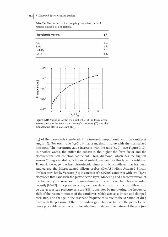
The most suitable piezoelectric material is PZT for piezoelectric bimorph micro-cantilevers (see Table 7.4 ). The form factor is a function of the Young ’ s modulus ( Y s ) the thickness ( h s ) of the substrate, the elastic constant ( C 11 ) and the thickness
Figure 7.9 Schematic of a piezoelectric bimorph cantilever.
Table 7.4 Electromechanical coupling coeffi cient ( K f2 ) of
various piezoelectric materials.
Piezoelectric material Kf2
AlN 1.03 ZnO 1.71 BaTiO 3 2.63 PZT4 3.47
Figure 7.10 Variation of the maximal value of the form factor versus the ratio the substrate ’ s Young ’ s modulus ( Y s ) and the piezoelectric elastic constant ( C 11 ).
0 2 4 6 8 104x102
6x10²
8x10²
1x10³
1x10³
F m
ax (
a.u.
)
Ys/C
11
Table 7.5 ) [88] . The bimorph cantilevers are also sensitive to temperature. It has been shown that the determination of the frequency shift of two resonant modes can be used to determine simultaneously both pressure and temperature of a gas [89] . We have also made and operated diamond/AlN microcantilevers as gas pres-sure sensors [83] . The variation of the impedance of the fi rst resonant frequency of the diamond/AlN as a function of nitrogen gas pressure is plotted on Figure 7.11 . The resonant frequency decreases nearly linearly with the increasing pres-sure of nitrogen (see Figure 7.12 ) with a sensitivity of ∼ 4.2 ppm/mbar for nitrogen pressure up to 7 bars and at center frequency f ∼ 36.5 kHz.
7.5 Conclusion
In this chapter, we have briefl y reviewed the different types of acoustic devices with special attention to sensor applications. Despite the fact that acoustic sensors have been already used to study physical and chemical properties of gases and liquids for decades, the use of diamond in this fi eld is new. We have discussed
Table 7.5 Pressure sensitivity of a S i / Z n O microcantilever in different gases for the fi rst and the third resonant vibration mode [88] .
1st resonant vibration mode (ppm/mbar)
3rd resonant vibration mode (ppm/mbar)
Argon 5.7 4.5 Nitrogen 4.2 3.4 Helium 0.7 0.6
Figure 7.11 Impedance variation of a diamond/AlN microcantilever at the fi rst resonant mode as function of nitrogen pressure.( cantilever length ∼ 200 µ m, cantilever wide ∼ 50 µ m, diamond thickness ∼ 650 ν m and AlN thickness ∼ 1 µ m).
34500 35000 35500 36000 36500 37000
88.0k
90.0k
92.0k
94.0k
Impe
danc
e m
oulu
s (Ω
)
Frequency (Hz)
1.5 bar 2.5 bar 3.5 bar 4.5 bar 5.5 bar 6.5 bar
(a)
34000 34500 35000 35500 36000 36500 37000
-90.00
-89.75
-89.50
-89.25
-89.00
-88.75
-88.50
-88.25
Frequency (Hz)
1.5 bar 2.5 bar 3.5 bar 4.5 bar 5.5 bar 6.5 bar
(b)
7.5 Conclusion 193
194 7 Diamond-Based Acoustic Devices
and shown the interest to use diamond in composite acoustic devices: SAW fi lters, PFW sensors, TSM sensors, FBAR sensor and microcantilever sensors. While diamond - based SAW fi lter technology is mature, diamond - based acoustic sensors are still in their infancy and should not be neglected. The specifi c combination of exceptional properties of diamond: high mechanical properties, chemical stability, bio - inertness are highly desirable for the new generation of chemical and biologi-cal sensors.
References
Figure 7.12 Variation of the fi rst mode ’ s resonant frequency as a function of the nitrogen pressure for a diamond/AlN micro - cantilever.
1 2 3 4 5 6 7
35200
35400
35600
35800
36000
36200
Res
onan
t fre
quen
cy (
Hz)
Pressure (bar)
1 Curie , J. and Curie , P. ( 1880 ) Bulletin de
la Soci é t é fran ç aise de Min é ralogie , 3 , 90 . 2 Lord Rayleigh ( 1885 ) Proceedings of the
London Mathematical Society , s1-17 , 4 . 3 White , R.M. and Voltmer , F.W. ( 1965 )
Applied Physics Letters , 7 , 314 . 4 Wohltjen , H. and Dessy , R. ( 1979 )
Analytical Chemistry , 51 , 1458 . 5 Wenmackers , S. , Christiaens , P. ,
Daenen , M. , Haenen , K. , Nesl á dek , M. , van deVen , M. , Vermeeren , V. , Michiels , L. , Ameloot , M. and Wagner , P. ( 2005 ) physica status solidi (a) , 202 , 2212 .
6 Hernando , J. , Pourrostami , T. , Garrido , J.A. , Williams , O.A. , Gruen , D.M. , Romka , A. , Teinm ü ller , D. and Tutzmann , M. ( 2007 ) Diamond and
Related Materials , 16 , 138 . 7 Wang , J. and Carlisle , J.A. ( 2006 )
Diamond and Related Materials , 15 , 279 .
8 Aikawa , Y. and Baba , K. ( 1993 ) Japanese
Journal of Applied Physics , 32 , 4680 . 9 Field , J.E. (ed.) ( 1979 ) The Properties of
30 Wang , J.S. , Lakin , K.M. and Landin , A.R. ( 1983 ) Frequency Control, 37th Annual Symposium , 144 .
31 Gabl , R. , Schreiter , M. , Green , E. , Feucht , H.D. , Zeininger , H. , Runck , J. , Reichl , W. , Primig , R. , Pitzer , D. , Eckstein , G. and Wersing , W. ( 2003 ) Proceedings IEEE Sensors , 1184 .
32 Love , A.E.H. ( 1911 ) Some Problems of
Geodynamics , Cambridge (England) , University Press , 1911 .
Letters , 64 , 2894 . 34 Bjurstr ö m , J. , Wingqvist , G. , Yantchev , V.
and Katardjiev , I. ( 2007 ) Journal of
Micromechanics and Microengineering , 17 , 651 .
35 Yamanouchi , K. , Sakurai , N. and Satoh , T. ( 1989 ) IEEE Ultrasonics Symposium , 351 .
36 Shikata , S. - I. , Nakahata , H. , Hachigo , A. and Narita , M. ( 2005 ) Diamond and Related
Materials , 14 , 167 . 37 Chen , J.J. , Zeng , F. , Li , D.M. , Niu , J.B. and
Pan , F. ( 2005 ) Thin Solid Films , 485 , 257 . 38 Tang , I. - T. , Chen , H. - J. , Hwang , W.C. ,
Wang , Y.C. , Houng , M. - P. and Wang , Y. - H. ( 2004 ) Journal of Crystal Growth , 262 , 461 .
39 Shikata , S. - I. , Nakahata , H. and Hachigo , A. ( 1999 ) New Diamond and Frontier
Carbon Technology , 9 , 75 . 40 Mortet , V. , Elmazria , O. , Nesladek , M. ,
D ’ Haen , J. , Vanhoyland , G. , Elhakiki , M. , Tajani , A. , Bustarret , E. , Gheeraert , E. , D ’ Olieslaeger , M. and Alnot , P. ( 2003 ) Diamond and Related Materials , 12 , 723 .
41 Ishihara , M. , Manabe , T. , Kumagai , T. , Nakamura , T. , Fujiwara , S. , Ebata , Y. , Shikata , S. - I. , Nakahata , H. , Hachigo , A. and Koga , Y. ( 2001 ) Japanese Journal of
Applied Physics , 40 , 5065 . 42 Nakahata , H. , Hachigo , A. , Higaki , K. , Fujii ,
S. , Shikata , S. - I. and Fujimori , N. ( 1995 ) IEEE Transactions on Ultrasonics,
Ferroelectrics, and Frequency Control , 42 , 362 . 43 Higaki , K. , Nakahata , H. , Kitabayashi , H. ,
Fujii , S. , Tanabe , K. , Seki , Y. and Shikata , S. - I. ( 1997 ) IEEE Transactions on
Ultrasonics, Ferroelectrics, and Frequency
Control , 44 , 1395 . 44 Ishihara , M. , Nakamura , T. , Kokai , F. and
Koga , Y. ( 2002 ) Diamond and Related
Materials , 11 , 408 .
196 7 Diamond-Based Acoustic Devices
45 Elmazria , O. , Mortet , V. , Hakiki , M. El , Nesladek , M. and Alnot , P. ( 2003 ) IEEE
transactions on Ultrasonics, Ferroelectrics,
and Frequency Control , 50 , 710 . 46 Kirsch , P. , Assouar , M.B. , Elmazria , O. ,
Mortet , V. and Alnot , P. ( 2006 ) Applied
Physics Letters , 88 , 22350 . 47 Benetti , M. , Cannat à , D. , Di Pietrantonio ,
F. , Fedosov , V.I. and Verona , E. ( 2005 ) Applied Physics Letters , 87 , 033504 .
48 Fujii , S. , Shikata , S. , Member , T. Uemura , Nakahata , H. and Harima , H. ( 2005 ) IEEE Transactions on Ultrasonics,
Ferroelectrics, and Frequency Control , 52 , 1817 .
49 Uemura , T. , Fujii , S. , Kitabayashi , H. , Itakura , K. , Hachigo , A. , Nakahata , H. , Shikata , S. , Ishibashi , K. and Imai , T. ( 2002 ) Ultrasonics Symposium Proceedings , 431 .
50 Elmazria , O. , Hakiki , M. El , Mortet , V. , Assouar , B.M. , Nesladek , M. , Vanecek , M. , Bergonzo , P. and Alnot , P. ( 2004 ) IEEE Transactions on Ultrasonics,
Ferroelectrics, and Frequency Control , 51 , 1704 .
51 Benetti , M. , Cannata , D. , D ’ Amico , A. , Di Pietrantonio , F. , Macagnano , A. and Verona , E. ( 2004 ) Sensors, Proceedings of IEEE , 753 .
52 Weinberg , M.S. , Cunningham , B.T. and Clapp , C.W. ( 2000 ) Journal of
G. - A. , Gretillat , M. - A. , de Rooij , N.F. , Brooks , K.G. and Setter , N. ( 1998 ) Sensors and Actuators A , 64 , 41 .
54 Laurent , T. , Bastien , F.O. , Pommier , J. - C. , Cachard , A. , Remiens , D. and Cattan , E. ( 2000 ) Sensors and Actuators , 87 , 26 .
55 Choujaa , A. , Tirole , N. , Bonjour , C. , Martin , G. , Hauden , D. , Blind , P. , Cachard , A. and Pommier , C. ( 1995 ) Sensor and Actuators A , 46 , 179 .
56 Francis , L.A. , Kromka , A. , Steinmuller - Nethl , D. , Bertrand , P. and Van Hoof , C. ( 2006 ) IEEE Sensors Journal , 6 , 916 .
57 Hupert , M. , Muck , A. , Wang , R. , Stotter , J. , Cvackova , Z. , Haymond , S. , Show , Y. and Swain , G.M. ( 2003 ) Diamond and
Related Materials , 12 , 1940 . 58 Bragg , W.L. and Gibbs , R.E. ( 1925 )
Proceedings of the Royal Society A , 109 , 405 .
59 Zhang , Y.R. , Asahina , S. , Yoshihara , S. and Shirakashi , T. ( 2002 ) Journal of the
Electrochemical Society , 149 , H179 . 60 Damjanovic , D. ( 1998 ) Current Opinion in
Solid State and Materials Science , 3 , 469 . 61 Williams , O.A. , Mortet , V. , Daenen , M.
and Haenen , K. ( 2007 ) Applied Physics
Letters , 90 , 063514. 62 Á lvarez , D. , Fouchier , M. , Kretz , J. ,
Hartwich , J. , Schoemann , S. and Vandervorst , W. ( 2004 ) Microelectronic