49
1 Summary Notes Name……………………………………………… Class…………………… Physics CfE Higher Unit 3: Electricity CfE Higher
1
Summary
Notes
Name……………………………………………… Class……………………
Physics
CfE Higher
Unit 3: Electricity
CfE Higher
2
3.1 Electrons and Energy
Monitoring and measuring alternating current
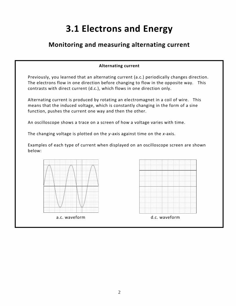
Alternating current Previously, you learned that an alternating current (a.c.) periodically changes direction. The electrons flow in one direction before changing to flow in the opposite way. This contrasts with direct current (d.c.), which flows in one direction only. Alternating current is produced by rotating an electromagnet in a coil of wire. This means that the induced voltage, which is constantly changing in the form of a sine function, pushes the current one way and then the other. An oscilloscope shows a trace on a screen of how a voltage varies with time. The changing voltage is plotted on the y-axis against time on the x-axis. Examples of each type of current when displayed on an oscilloscope screen are shown below:
a.c. waveform d.c. waveform
3
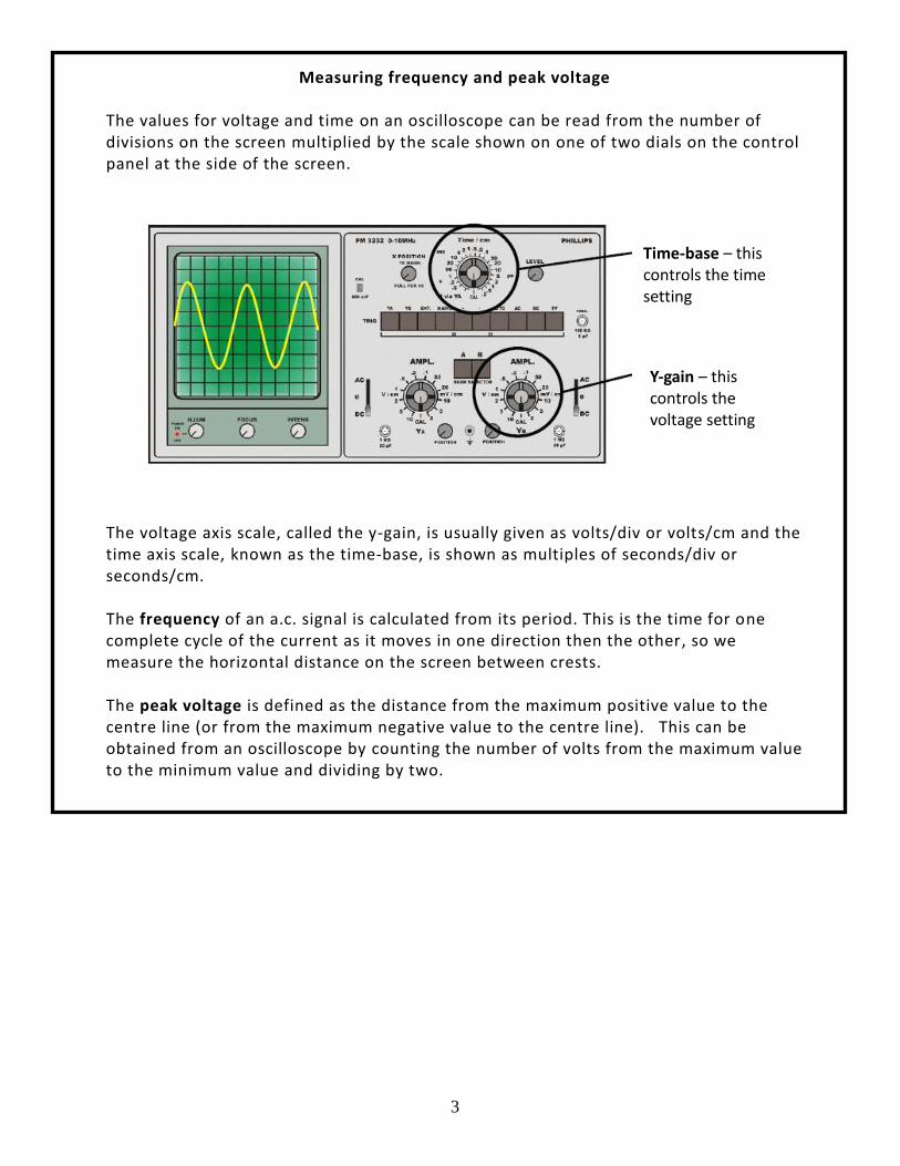
Measuring frequency and peak voltage The values for voltage and time on an oscilloscope can be read from the number of divisions on the screen multiplied by the scale shown on one of two dials on the control panel at the side of the screen.
The voltage axis scale, called the y-gain, is usually given as volts/div or volts/cm and the time axis scale, known as the time-base, is shown as multiples of seconds/div or seconds/cm. The frequency of an a.c. signal is calculated from its period. This is the time for one complete cycle of the current as it moves in one direction then the other, so we measure the horizontal distance on the screen between crests. The peak voltage is defined as the distance from the maximum positive value to the centre line (or from the maximum negative value to the centre line). This can be obtained from an oscilloscope by counting the number of volts from the maximum value to the minimum value and dividing by two.
Time-base – this controls the time setting
Y-gain – this controls the voltage setting

4
Worked example Calculate (i) the frequency and (ii) the peak voltage of the waveform shown on the CRO screen below. Each box on the CRO screen has a side of length 1 cm.
(i) Frequency: (ii) Peak Voltage: The distance between crests is 4 cm. The distance from bottom to top is 8 cm. The time base is set at 5 ms cm–1, The volts/div is set at 2 V cm–1, Period, T = 4 × 5 ms = 4 × 0.005 = 0.02 s Vpeak = ½ × 8 × 2
Tf
1
02.0
1 = 50 Hz Vpeak = 8 V
Timebase switched off
If the time base is switched off, the a.c. signal will not spread along the x-axis. However, the voltage variation will continue to oscillate up and down, meaning a straight vertical line will be displayed on the screen. The height of this line from bottom to top can be processed in exactly the same way as above, ie halved then converted into voltage using the volts/div.
Timebase = 5 ms
Volts/div = 2 V cm–1
5
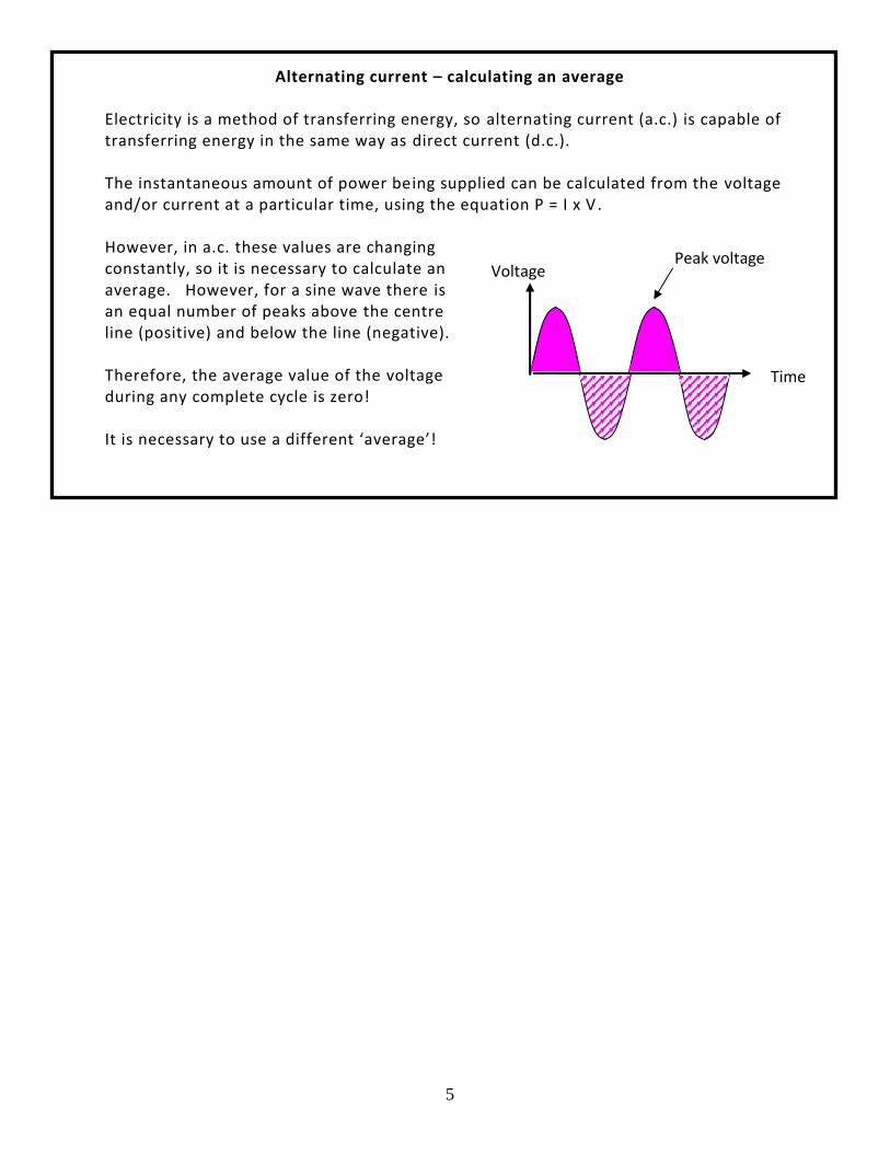
Alternating current – calculating an average Electricity is a method of transferring energy, so alternating current (a.c.) is capable of transferring energy in the same way as direct current (d.c.). The instantaneous amount of power being supplied can be calculated from the voltage and/or current at a particular time, using the equation P = I x V . However, in a.c. these values are changing constantly, so it is necessary to calculate an average. However, for a sine wave there is an equal number of peaks above the centre line (positive) and below the line (negative). Therefore, the average value of the voltage during any complete cycle is zero! It is necessary to use a different ‘average’!
Time
Voltage Peak voltage
6
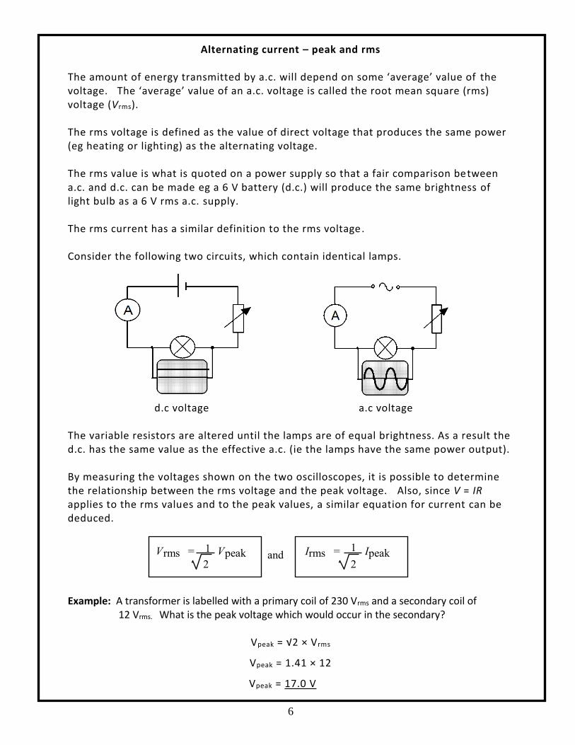
Alternating current – peak and rms The amount of energy transmitted by a.c. will depend on some ‘average’ value of the voltage. The ‘average’ value of an a.c. voltage is called the root mean square (rms) voltage (Vrms). The rms voltage is defined as the value of direct voltage that produces the same power (eg heating or lighting) as the alternating voltage. The rms value is what is quoted on a power supply so that a fair comparison between a.c. and d.c. can be made eg a 6 V battery (d.c.) will produce the same brightness of light bulb as a 6 V rms a.c. supply. The rms current has a similar definition to the rms voltage. Consider the following two circuits, which contain identical lamps. d.c voltage a.c voltage The variable resistors are altered until the lamps are of equal brightness. As a result the d.c. has the same value as the effective a.c. (ie the lamps have the same power output). By measuring the voltages shown on the two oscilloscopes, it is possible to determine the relationship between the rms voltage and the peak voltage. Also, since V = IR applies to the rms values and to the peak values, a similar equation for current can be deduced. Example: A transformer is labelled with a primary coil of 230 Vrms and a secondary coil of
12 Vrms. What is the peak voltage which would occur in the secondary?
Vpeak = √2 × Vrms
Vpeak = 1.41 × 12
Vpeak = 17.0 V
I peak I = 1
2
V peak V = 1
2
and rms rms
7
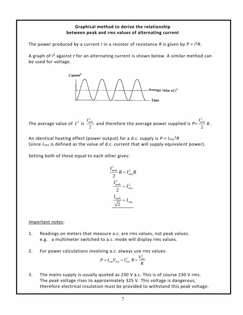
Graphical method to derive the relationship
between peak and rms values of alternating current The power produced by a current I in a resistor of resistance R is given by P = I2R. A graph of I2 against t for an alternating current is shown below. A similar method can be used for voltage.
The average value of 2I is 2
peak
2
I and therefore the average power supplied is P=
2
peak
2
IR .
An identical heating effect (power output) for a d.c. supply is P = Irms
2R (since Irms is defined as the value of d.c. current that will supply equivalent power). Setting both of these equal to each other gives:
2
peak 2
rms2
IR I R
2
peak 2
rms2
II
peak
rms2
II
Important notes: 1. Readings on meters that measure a.c. are rms values, not peak values . e.g. a multimeter switched to a.c. mode will display rms values. 2. For power calculations involving a.c. always use rms values:
22 rms
rms rms rms
VP I V I R
R
3. The mains supply is usually quoted as 230 V a.c. This is of course 230 V rms.
The peak voltage rises to approximately 325 V. This voltage is dangerous, therefore electrical insulation must be provided to withstand this peak voltage.
8
Current, voltage, power and resistance
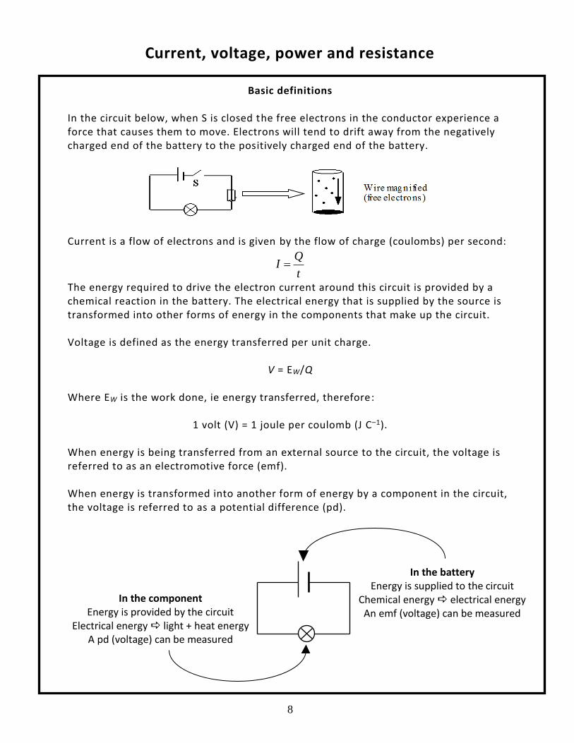
Basic definitions In the circuit below, when S is closed the free electrons in the conductor experience a force that causes them to move. Electrons will tend to drift away from the negatively charged end of the battery to the positively charged end of the battery.
Current is a flow of electrons and is given by the flow of charge (coulombs) per second:
t
QI
The energy required to drive the electron current around this circuit is provided by a chemical reaction in the battery. The electrical energy that is supplied by the source is transformed into other forms of energy in the components that make up the circuit. Voltage is defined as the energy transferred per unit charge.
V = EW/Q
Where EW is the work done, ie energy transferred, therefore:
1 volt (V) = 1 joule per coulomb (J C–1). When energy is being transferred from an external source to the circuit, the voltage is referred to as an electromotive force (emf). When energy is transformed into another form of energy by a component in the circuit, the voltage is referred to as a potential difference (pd).
In the battery Energy is supplied to the circuit
Chemical energy electrical energy An emf (voltage) can be measured
In the component Energy is provided by the circuit
Electrical energy light + heat energy A pd (voltage) can be measured
9
Sources of emf Emfs can be generated in a great variety of ways. See the table below for examples.
Chemical cell Chemical energy drives the current
(eg battery)
Thermocouple Heat energy drives the current
(eg temperature sensor in an oven)
Piezo-electric generator Mechanical vibrations drive the current
(eg acoustic guitar pickup)
Solar cell Light energy drives the current
(eg solar panels on a house)
Electromagnetic generator Changes in magnetic field drive the current
(eg power stations)
Ohm’s law
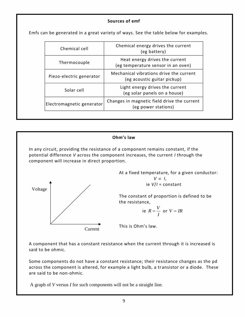
In any circuit, providing the resistance of a component remains constant, if the potential difference V across the component increases, the current I through the component will increase in direct proportion.
At a fixed temperature, for a given conductor: V I,
ie V/I = constant The constant of proportion is defined to be the resistance,
ie I
VR or IRV
This is Ohm’s law.
A component that has a constant resistance when the current through it is increased is said to be ohmic. Some components do not have a constant resistance; their resistance changes as the pd across the component is altered, for example a light bulb, a transistor or a diode. These are said to be non-ohmic. A graph of V versus I for such components will not be a straight line.
Current
Voltage
10
Circuit rules
You must be able to apply the circuit rules that you learned last year to series and parallel circuits, both alone and in combination. The circuit rules are summarized in the table below:
Series Parallel
Current S 1 2 3I I I I 321 IIIIS
Voltage S 1 2 3V V V V 321 VVVVS
Resistance 321 RRRRT 321
1111
RRRRT
where VS = supply voltage, IS = current from the supply and RT = total resistance
Examples:
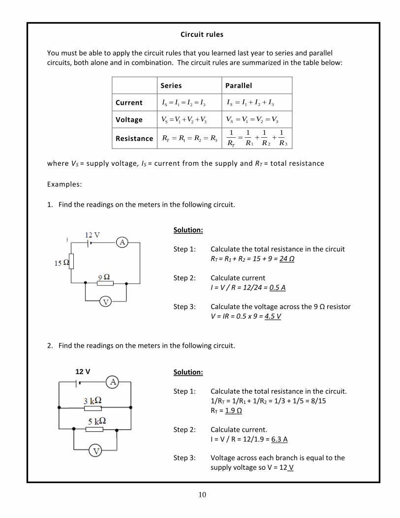
1. Find the readings on the meters in the following circuit.
2. Find the readings on the meters in the following circuit.
Solution: Step 1: Calculate the total resistance in the circuit RT = R1 + R2 = 15 + 9 = 24 Ω Step 2: Calculate current
I = V / R = 12/24 = 0.5 A Step 3: Calculate the voltage across the 9 Ω resistor
V = IR = 0.5 x 9 = 4.5 V
12 V Solution: Step 1: Calculate the total resistance in the circuit.
1/RT = 1/R1 + 1/R2 = 1/3 + 1/5 = 8/15 RT = 1.9 Ω
Step 2: Calculate current.
I = V / R = 12/1.9 = 6.3 A
Step 3: Voltage across each branch is equal to the supply voltage so V = 12 V
11
Electric power
The power is defined as the electrical energy transferred in one second:
work donepower
time
QV QV IV
t t
Therefore, P= I x V
From Ohm’s law, V = I x R and R
VI
Substituting, P = I × IR VR
VP
Therefore, P = I2R PR
V 2
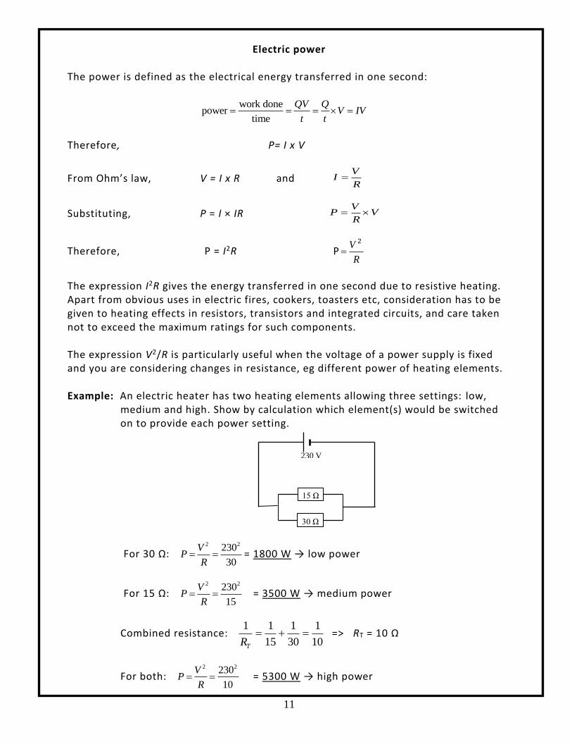
The expression I2R gives the energy transferred in one second due to resistive heating. Apart from obvious uses in electric fires, cookers, toasters etc, consideration has to be given to heating effects in resistors, transistors and integrated circuits, and care taken not to exceed the maximum ratings for such components. The expression V2/R is particularly useful when the voltage of a power supply is fixed and you are considering changes in resistance, eg different power of heating elements. Example: An electric heater has two heating elements allowing three settings: low,
medium and high. Show by calculation which element(s) would be switched on to provide each power setting.
For 30 Ω: 2 2230
30
VP
R = 1800 W → low power
For 15 Ω: 2 2230
15
VP
R = 3500 W → medium power
Combined resistance: 10
1
30
1
15
11
TR => RT = 10 Ω
For both: 2 2230
10
VP
R = 5300 W → high power
15 Ω
230 V
30 Ω

12
R
R
≡ ½R
Addition of power By conservation of energy, the total power used in both series and parallel circuits is the sum of the power used in each component. Example: Calculate the total power dissipated in each of the following circuits a) Step 1: Calculate the total current in circuit
I=VS/RT = 9 / 18 = 0.5 A
Step 2: Calculate power in each resistor P1 = I2R = 0.52 x 12 = 3 W P2 = I2R = 0.52 x 6 = 1.5 W
Step 3: Calculate total power PT = P1 + P2 = 3 + 1.5 = 4.5 W
b) Step 1: Calculate power in each resistor P1 = V2/R = 122 / 24 = 6 W P2 = V2/R = 122 / 6 = 24 W Step 2: Calculate total power
PT = P1 + P2 = 6 + 24 = 30 W
Identical resistors in parallel
Two resistors of the same value (R) wired in parallel: RP = half the value of one of them (½R). Examples: 2 × 1000 Ω in parallel, RT = 500 Ω 2 × 250 Ω in parallel, RT = 125 Ω
13
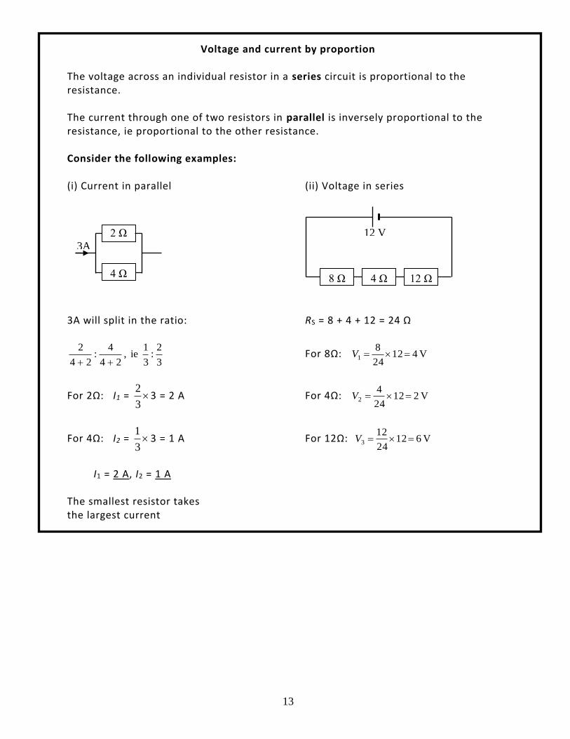
Voltage and current by proportion The voltage across an individual resistor in a series circuit is proportional to the resistance. The current through one of two resistors in parallel is inversely proportional to the resistance, ie proportional to the other resistance. Consider the following examples: (i) Current in parallel (ii) Voltage in series
3A will split in the ratio: RS = 8 + 4 + 12 = 24 Ω
3
2:
3
1 ie ,
24
4:
24
2
For 8Ω: V 412
24
81 V
For 2Ω: I1 = 3
23 = 2 A For 4Ω: V 212
24
42 V
For 4Ω: I2 = 3
13 = 1 A For 12Ω: V 612
24
123 V
I1 = 2 A, I2 = 1 A
The smallest resistor takes the largest current
8 Ω 4 Ω 12 Ω
12 V 2 Ω
4 Ω
3A
14
6 Ω 4 Ω
5 Ω
40 V
10 Ω
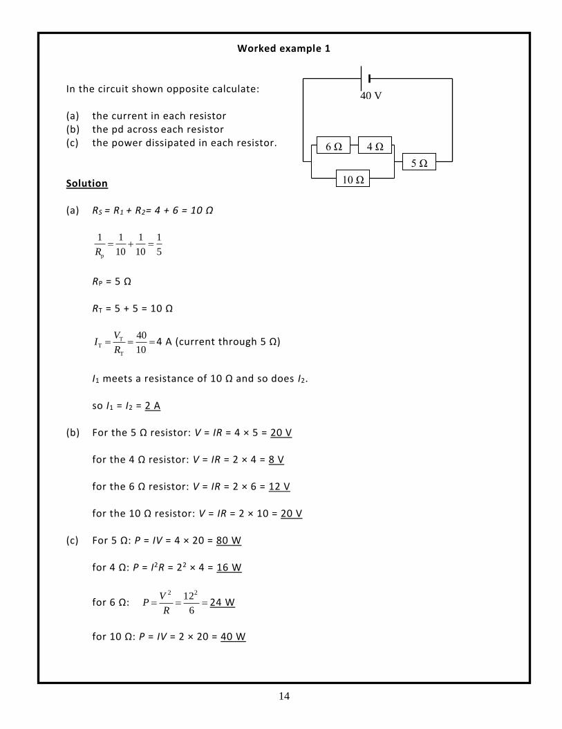
Worked example 1
In the circuit shown opposite calculate: (a) the current in each resistor (b) the pd across each resistor (c) the power dissipated in each resistor. Solution (a) RS = R1 + R2= 4 + 6 = 10 Ω
p
1 1 1 1
10 10 5R
RP = 5 Ω RT = 5 + 5 = 10 Ω
TT
T
40
10
VI
R 4 A (current through 5 Ω)
I1 meets a resistance of 10 Ω and so does I2. so I1 = I2 = 2 A (b) For the 5 Ω resistor: V = IR = 4 × 5 = 20 V
for the 4 Ω resistor: V = IR = 2 × 4 = 8 V
for the 6 Ω resistor: V = IR = 2 × 6 = 12 V
for the 10 Ω resistor: V = IR = 2 × 10 = 20 V (c) For 5 Ω: P = IV = 4 × 20 = 80 W for 4 Ω: P = I2R = 22 × 4 = 16 W
for 6 Ω: 6
1222
R
VP 24 W
for 10 Ω: P = IV = 2 × 20 = 40 W
15
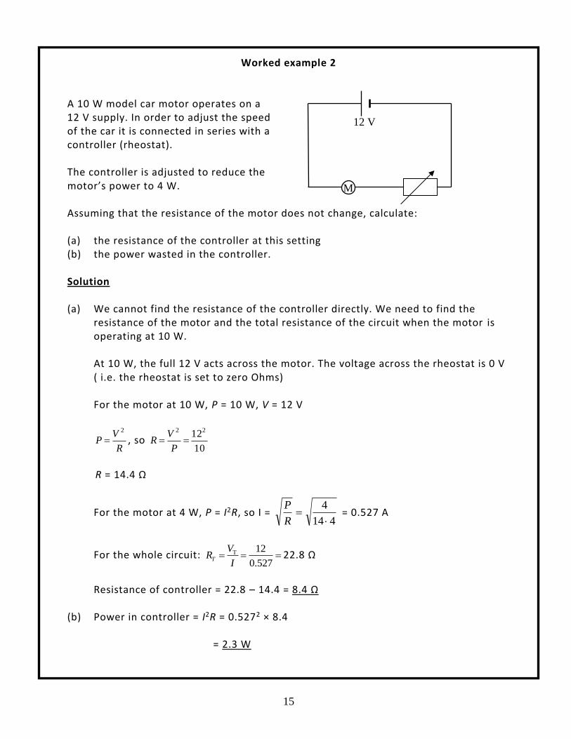
Worked example 2
A 10 W model car motor operates on a 12 V supply. In order to adjust the speed of the car it is connected in series with a controller (rheostat). The controller is adjusted to reduce the motor’s power to 4 W. Assuming that the resistance of the motor does not change, calculate: (a) the resistance of the controller at this setting (b) the power wasted in the controller. Solution (a) We cannot find the resistance of the controller directly. We need to find the
resistance of the motor and the total resistance of the circuit when the motor is operating at 10 W.
At 10 W, the full 12 V acts across the motor. The voltage across the rheostat is 0 V
( i.e. the rheostat is set to zero Ohms)
For the motor at 10 W, P = 10 W, V = 12 V
R
VP
2
, so 10
1222
P
VR
R = 14.4 Ω
For the motor at 4 W, P = I2R, so I = 414
4
R
P = 0.527 A
For the whole circuit: T 12
0.527T
VR
I 22.8 Ω
Resistance of controller = 22.8 – 14.4 = 8.4 Ω
(b) Power in controller = I2R = 0.5272 × 8.4 = 2.3 W
12 V
M
16
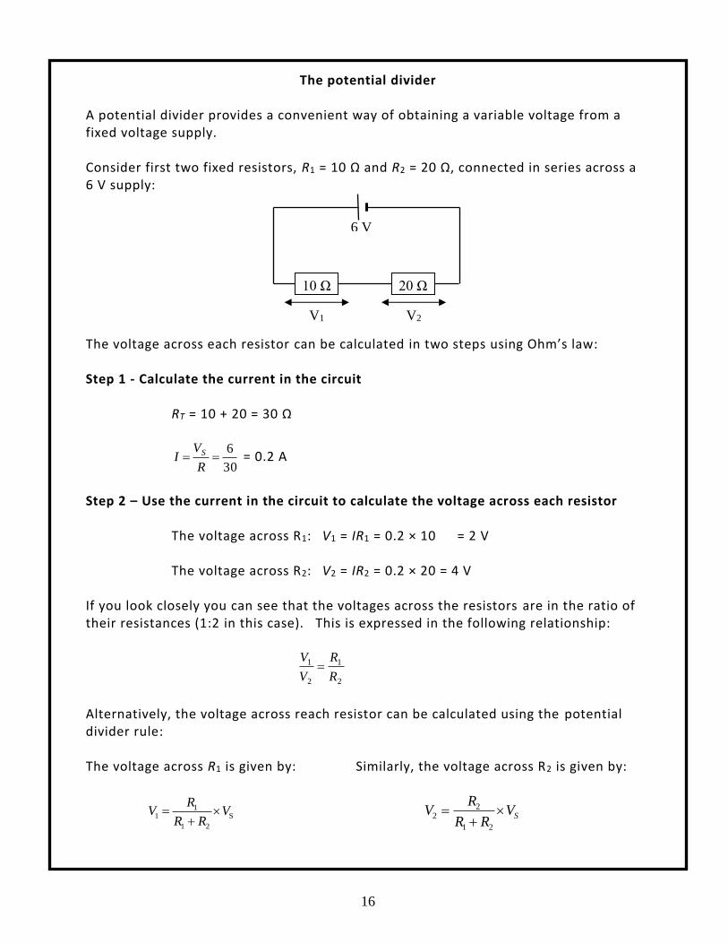
The potential divider
A potential divider provides a convenient way of obtaining a variable voltage from a fixed voltage supply. Consider first two fixed resistors, R1 = 10 Ω and R2 = 20 Ω, connected in series across a 6 V supply:
The voltage across each resistor can be calculated in two steps using Ohm’s law: Step 1 - Calculate the current in the circuit RT = 10 + 20 = 30 Ω
30
6
R
VI S = 0.2 A
Step 2 – Use the current in the circuit to calculate the voltage across each resistor The voltage across R1: V1 = IR1 = 0.2 × 10 = 2 V The voltage across R2: V2 = IR2 = 0.2 × 20 = 4 V If you look closely you can see that the voltages across the resistors are in the ratio of their resistances (1:2 in this case). This is expressed in the following relationship:
2
1
2
1
R
R
V
V
Alternatively, the voltage across reach resistor can be calculated using the potential divider rule: The voltage across R1 is given by: Similarly, the voltage across R2 is given by:
11 S
1 2
RV V
R R
SV
RR
RV
21
22
10 Ω 20 Ω
6 V
V1 V2
17
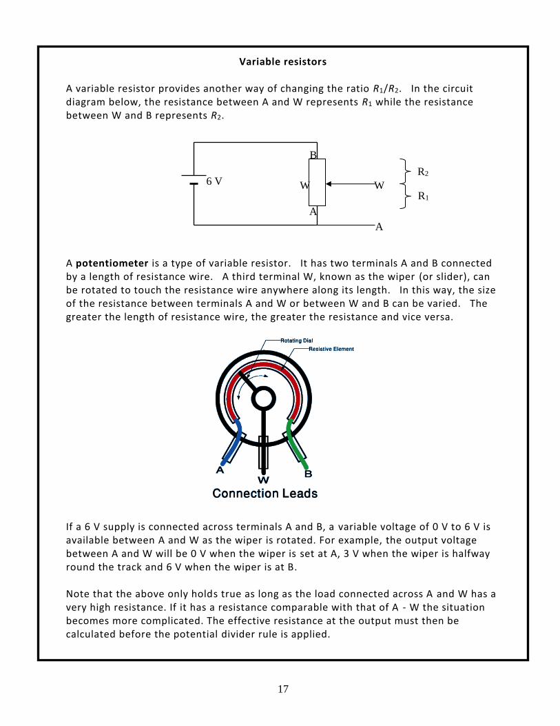
Variable resistors
A variable resistor provides another way of changing the ratio R1/R2. In the circuit diagram below, the resistance between A and W represents R1 while the resistance between W and B represents R2.
A potentiometer is a type of variable resistor. It has two terminals A and B connected by a length of resistance wire. A third terminal W, known as the wiper (or slider), can be rotated to touch the resistance wire anywhere along its length. In this way, the size of the resistance between terminals A and W or between W and B can be varied. The greater the length of resistance wire, the greater the resistance and vice versa.
If a 6 V supply is connected across terminals A and B, a variable voltage of 0 V to 6 V is available between A and W as the wiper is rotated. For example, the output voltage between A and W will be 0 V when the wiper is set at A, 3 V when the wiper is halfway round the track and 6 V when the wiper is at B. Note that the above only holds true as long as the load connected across A and W has a very high resistance. If it has a resistance comparable with that of A - W the situation becomes more complicated. The effective resistance at the output must then be calculated before the potential divider rule is applied.
A
W W
A
6 V
B
R2
R1

18
Worked example Consider the following voltage divider circuit:
(a) Calculate the voltage across XY.
R1 = 10 kΩ R2 = 20 kΩ VS = 12 V V1 = ?
(b) The circuit attached to XY has a resistance of 10 kΩ as shown below. Calculate the
effective resistance between XY and thus the voltage across XY.
The resistance between XY comes from the two identical 10 kΩ resistors in parallel. The combined resistance is therefore 5 kΩ. Use this resistance as R1 in the potential divider formula.
R1 = 5 kΩ R2 = 20 kΩ VS = 12 V V1 = ?
10 kΩ
Y
X
12 V
20 kΩ
10 kΩ Y
X
12 V
20 kΩ
10 kΩ
SVRR
RV
21
11
122010
101
V
V1 = 4 V
SVRR
RV
21
11
12205
51
V
V1 = 2.4 V
19
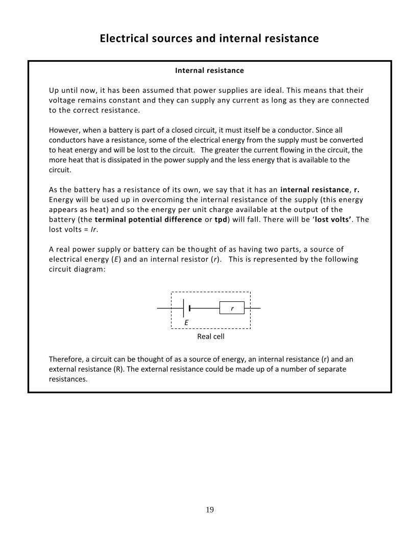
Electrical sources and internal resistance
Internal resistance
Up until now, it has been assumed that power supplies are ideal. This means that their voltage remains constant and they can supply any current as long as they are connected to the correct resistance. However, when a battery is part of a closed circuit, it must itself be a conductor. Since all conductors have a resistance, some of the electrical energy from the supply must be converted to heat energy and will be lost to the circuit. The greater the current flowing in the circuit, the more heat that is dissipated in the power supply and the less energy that is available to the circuit. As the battery has a resistance of its own, we say that it has an internal resistance, r. Energy will be used up in overcoming the internal resistance of the supply (this energy appears as heat) and so the energy per unit charge available at the output of the battery (the terminal potential difference or tpd) will fall. There will be ‘lost volts’. The lost volts = Ir. A real power supply or battery can be thought of as having two parts, a source of electrical energy (E) and an internal resistor (r). This is represented by the following circuit diagram:
Therefore, a circuit can be thought of as a source of energy, an internal resistance (r) and an external resistance (R). The external resistance could be made up of a number of separate resistances.
E
r
Real cell
20
E
r I = 0
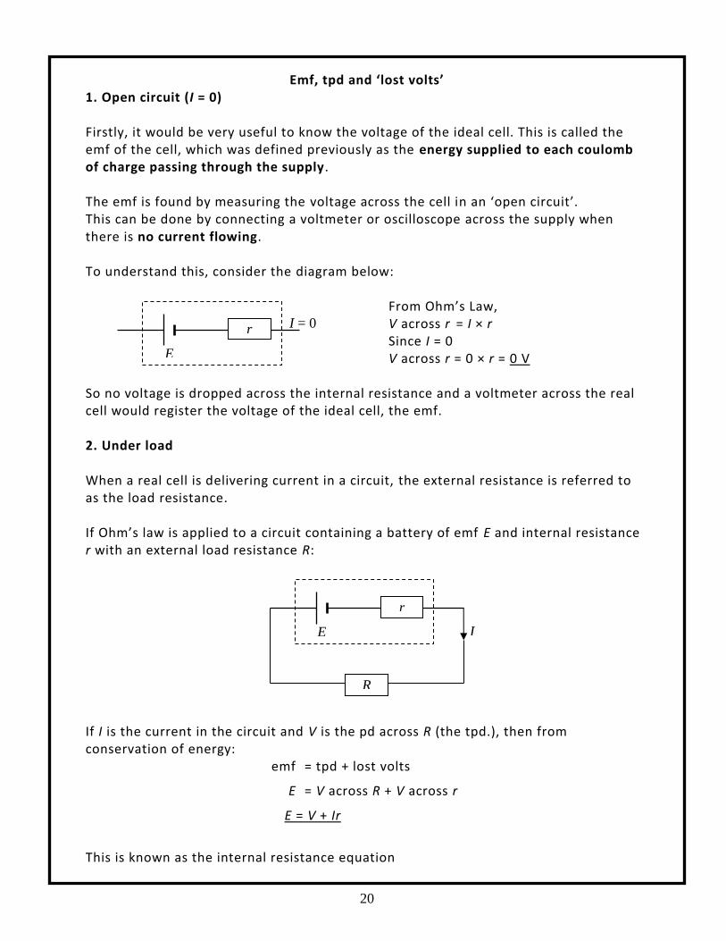
Emf, tpd and ‘lost volts’
1. Open circuit (I = 0) Firstly, it would be very useful to know the voltage of the ideal cell. This is called the emf of the cell, which was defined previously as the energy supplied to each coulomb of charge passing through the supply. The emf is found by measuring the voltage across the cell in an ‘open circuit’. This can be done by connecting a voltmeter or oscilloscope across the supply when there is no current flowing. To understand this, consider the diagram below: From Ohm’s Law,
V across r = I × r Since I = 0 V across r = 0 × r = 0 V
So no voltage is dropped across the internal resistance and a voltmeter across the real cell would register the voltage of the ideal cell, the emf. 2. Under load When a real cell is delivering current in a circuit, the external resistance is referred to as the load resistance. If Ohm’s law is applied to a circuit containing a battery of emf E and internal resistance r with an external load resistance R:
If I is the current in the circuit and V is the pd across R (the tpd.), then from conservation of energy: emf = tpd + lost volts
E = V across R + V across r
E = V + Ir
This is known as the internal resistance equation
E
r
I
R

21
E
r
11.4 Ω
V
0.6 Ω I = 0.5 A
The internal resistance equation can clearly be rearranged into different forms, for example:
E = V + Ir or V = E – Ir since V = IR,
E = IR + Ir or E = I(R + r) Consider the case of a cell with an internal resistance of 0.6 Ω delivering current to an external resistance of 11.4 Ω: Cell emf. = 6 V Current = 0.5 A The voltage measured across the terminals of the cell will be the voltage across the 11.4 Ω resistor: V = IR = 0.5 × 11.4 = 5.7 V and the voltage across the internal resistance: V = Ir = 0.5 × 0.6 = 0.3 V The voltage across the terminals is known as the terminal potential difference or tpd. This is only 5.7 V because of the 0.3 V voltage dropped across the internal resistance of the cell. This is called the lost volts. 3. Short circuit (R = 0) The maximum current is the short-circuit current. This is the current that will flow when the terminals of the supply are joined with a short piece of thick wire (ie there is no external resistance). By substituting R = 0 in the above equation we get:
E = I(0 + r)
E = Ir

22
E
r
R
V
I
Measuring E and r by a graphical methods
First graphical method When we increase the current in a circuit like the one shown below, the energy lost in the supply due to heating will increase. Therefore, the ‘lost volts’ will increase and the tpd will decrease. If we plot a graph of V on the y-axis against I on the x-axis, we get a straight line of negative gradient. We can use this graph to determine the emf and internal resistance: From the internal resistance equation,
V = E – Ir
Re-arranging,
V = (–r) × I + E Comparing this with the equation of a straight line,
y = mx + c The gradient of the line (m) is equivalent to –r and the y-intercept (c) is E.
Current
Voltage Gradient (m) = –r (internal resistance)
Intercept (c) = E (emf)
23
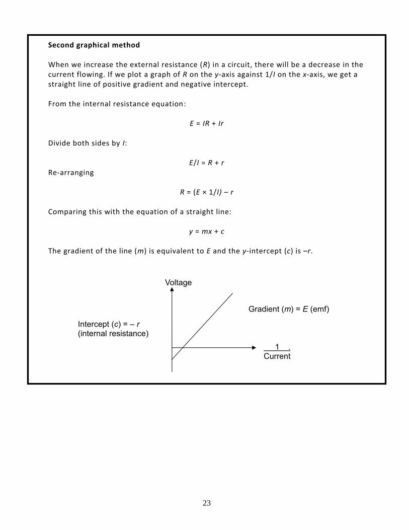
Second graphical method When we increase the external resistance (R) in a circuit, there will be a decrease in the current flowing. If we plot a graph of R on the y-axis against 1/I on the x-axis, we get a straight line of positive gradient and negative intercept. From the internal resistance equation:
E = IR + Ir Divide both sides by I:
E/I = R + r Re-arranging
R = (E × 1/I) – r Comparing this with the equation of a straight line:
y = mx + c The gradient of the line (m) is equivalent to E and the y-intercept (c) is –r.
1 . Current
Voltage
Gradient (m) = E (emf)
Intercept (c) = – r (internal resistance)

24
1.5 V
r
I 2 Ω
Worked example
A cell of emf 1.5 V is connected in series with a 28 Ω resistor. A voltmeter measures the voltage across the cell as 1.4 V.
Calculate: (a) the internal resistance of the cell (b) the current if the cell terminals are short circuited (c) the lost volts if the external resistance R is increased to 58 Ω. Solution: (a) E = V + Ir In this case we do not know the current, I, but we do know that the voltage across the 28 Ω resistor is 1.4 V, and I = V/R , so I = 0.05 A. 1.5 = 1.4 + 0.05r
05.0
1.0r 2 Ω
(b) Short circuit: Total resistance = 2 Ω
2
5.1
r
EI 0.75 A
(c) E = I(R + r) 1.5= I(58 + 2) I = 1.5/60 = 0.025 A lost volts = Ir = 0.025 × 2 = 0.05 V
E
r
28 Ω
V

25
Capacitors
Capacitance
Capacitance is the ability (or capacity) of a component to store charge. A device that stores charge is called a capacitor. Practical capacitors consist of two conducting layers separated by an insulator. The simplest type is two metal plates with an air gap between them. The circuit symbol for a capacitor is based on this:
Relationship between charge and pd
A capacitor is charged to a chosen voltage by setting the switch to A. The charge stored can be measured directly by discharging through the coulomb meter by moving the switch to B.
In this way pairs of readings of voltage and charge are obtained. When a graph of charge stored on the capacitor is plotted against the pd (voltage), it is found that the charge is directly proportional to the pd (voltage) across it:
Notice that this means that capacitance is the gradient of the above graph.
p.d.
Charge
0
From the graph:
Q V This constant is defined as the capacitance, C:
V
QC or Q = CV
= a constant
26
For any capacitor, the ration Q/V is a constant and is called the capacitance Therefore, the formal definition of capacitance is the charge stored per unit voltage. The unit of capacitance is the farad (F). From the above formula: 1 farad = 1 coulomb per volt. The farad is too large a unit for practical purposes and the following submultiples are used: 1 mF (microfarad) = 1 × 10⁻⁶ F and 1 nF (nanofarad) = 1 × 10⁻⁹ F Note: When a capacitor is charging, the current is not constant (more on this later). This means the formula Q = It cannot be used to work out the charge stored. Example: A capacitor stores 4 × 10⁻⁴ C of charge when the potential difference across
it is 100 V. Calculate the capacitance. Q = 4 x 10⁻⁴ C
V = 100 V 64
104100
104
V
QC F = 4 μF
C = ?
Capacitance = voltage
charge
farad (F)
Coulombs (C)
Volts (V)
27
Energy stored in a capacitor
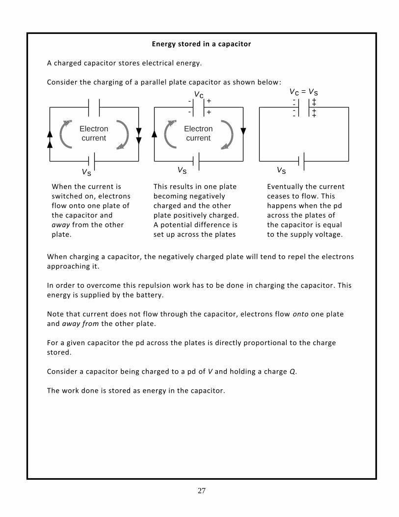
A charged capacitor stores electrical energy. Consider the charging of a parallel plate capacitor as shown below:
When charging a capacitor, the negatively charged plate will tend to repel the electrons approaching it. In order to overcome this repulsion work has to be done in charging the capacitor. This energy is supplied by the battery. Note that current does not flow through the capacitor, electrons flow onto one plate and away from the other plate. For a given capacitor the pd across the plates is directly proportional to the charge stored. Consider a capacitor being charged to a pd of V and holding a charge Q. The work done is stored as energy in the capacitor.
V s V s
Electron
current
V s
Electron
current
+ -
+ -
V c V c = V s
+ - + - + - + -
When the current is switched on, electrons flow onto one plate of the capacitor and away from the other plate.
This results in one plate becoming negatively charged and the other plate positively charged. A potential difference is set up across the plates
Eventually the current ceases to flow. This happens when the pd across the plates of the capacitor is equal to the supply voltage.
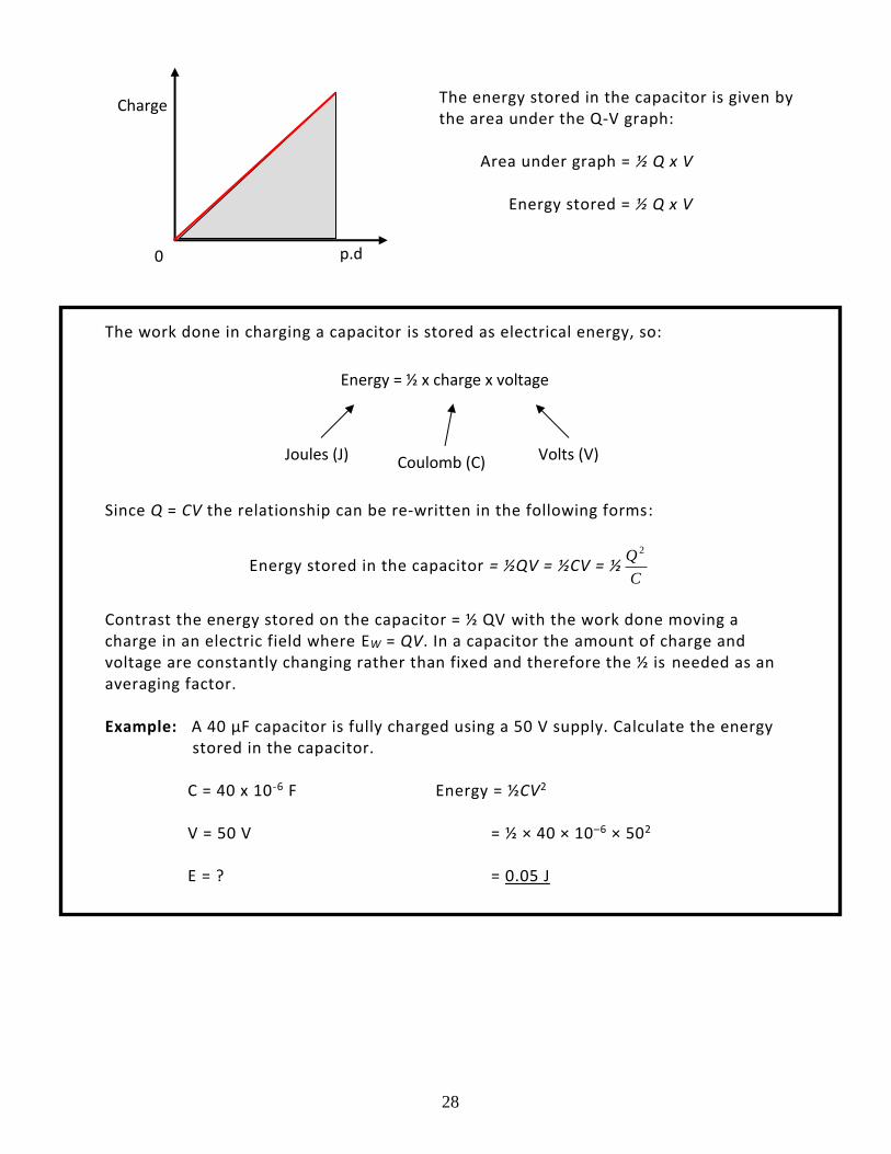
28
The work done in charging a capacitor is stored as electrical energy, so:
Since Q = CV the relationship can be re-written in the following forms:
Energy stored in the capacitor = ½QV = ½CV = ½C
Q 2
Contrast the energy stored on the capacitor = ½ QV with the work done moving a charge in an electric field where EW = QV. In a capacitor the amount of charge and voltage are constantly changing rather than fixed and therefore the ½ is needed as an averaging factor. Example: A 40 μF capacitor is fully charged using a 50 V supply. Calculate the energy
stored in the capacitor.
C = 40 x 10-6 F Energy = ½CV2
V = 50 V = ½ × 40 × 10–6 × 502
E = ? = 0.05 J
p.d.
Charge
0
Energy = ½ x charge x voltage
Joules (J) Coulomb (C) Volts (V)
The energy stored in the capacitor is given by the area under the Q-V graph: Area under graph = ½ Q x V Energy stored = ½ Q x V

29
Charging and discharging a capacitor
Charging Consider the following circuit: When the switch is closed the current flowing in the circuit and the voltage across the capacitor behave as shown in the graphs below:
Consider the circuit at three different times.
time
c urrent
0
Supply voltage
pd across capacitor
0 time
As soon as the switch is closed there is no charge on the capacitor. The current is limited only by the resistance in the circuit and can be found using Ohm’s law.
As the capacitor charges a pd develops across the plates which opposes the pd of the cell. As a result, the current from the supply decreases
The capacitor becomes fully charged and the pd across the plates is equal and opposite to that across the cell and the charging current becomes zero.
30
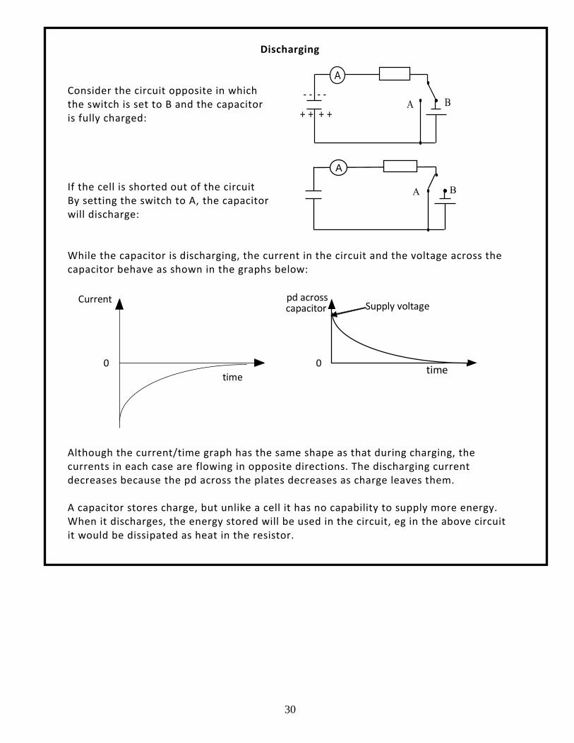
If the cell is taken out of the circuit and the switch is set to A, the capacitor will discharge
Consider this circuit when the capacitor is fully charged, switch to position B
A A
- - - -
+ + + +
B A A B
If the cell is taken out of the circuit and the switch is set to A, the capacitor will discharge
Consider this circuit when the capacitor is fully charged, switch to position B
A A
- - - -
+ + + +
B A A B
Discharging
Consider the circuit opposite in which the switch is set to B and the capacitor is fully charged: If the cell is shorted out of the circuit By setting the switch to A, the capacitor will discharge: While the capacitor is discharging, the current in the circuit and the voltage across the capacitor behave as shown in the graphs below: pd across
capacitor
time
Current
0 0 time
Supply voltage
Although the current/time graph has the same shape as that during charging, the currents in each case are flowing in opposite directions. The discharging current decreases because the pd across the plates decreases as charge leaves them. A capacitor stores charge, but unlike a cell it has no capability to supply more energy. When it discharges, the energy stored will be used in the circuit, eg in the above circuit it would be dissipated as heat in the resistor.
31
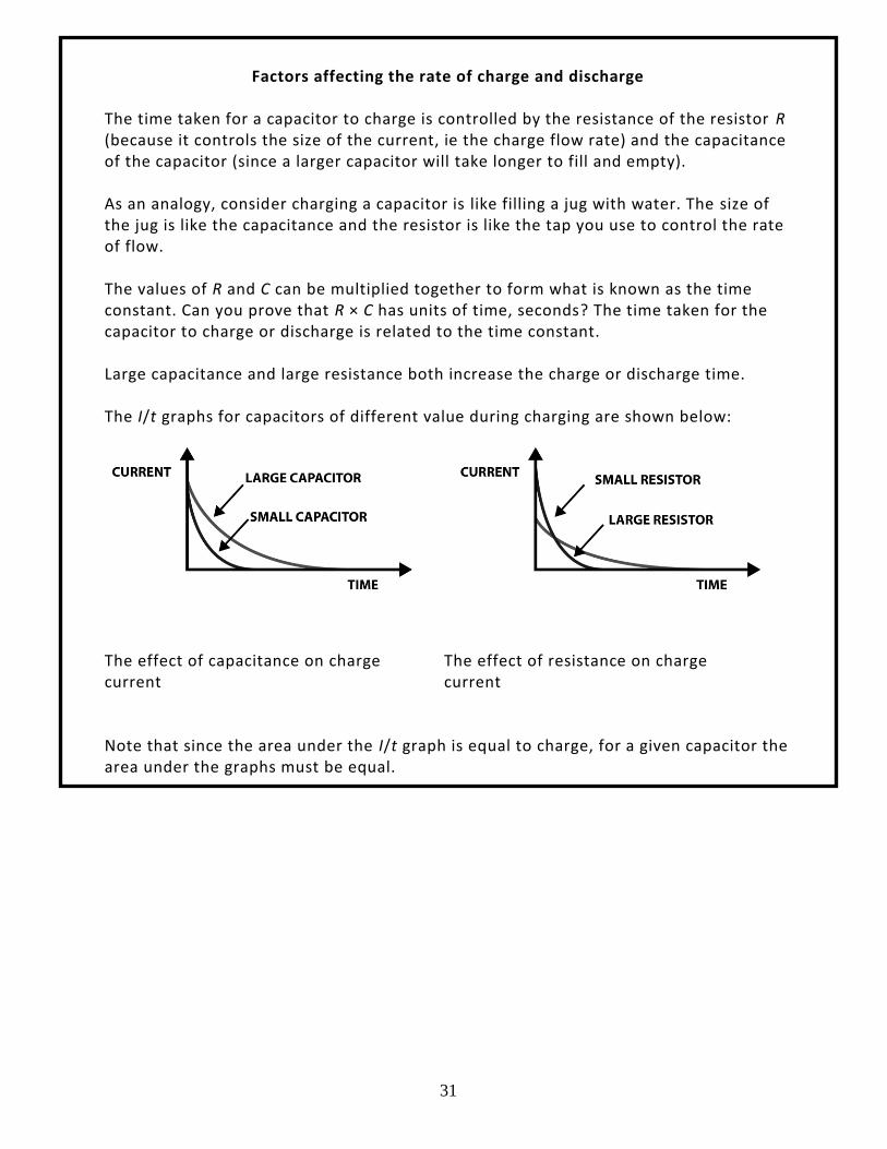
Factors affecting the rate of charge and discharge The time taken for a capacitor to charge is controlled by the resistance of the resistor R (because it controls the size of the current, ie the charge flow rate) and the capacitance of the capacitor (since a larger capacitor will take longer to fill and empty). As an analogy, consider charging a capacitor is like filling a jug with water. The size of the jug is like the capacitance and the resistor is like the tap you use to control the rate of flow. The values of R and C can be multiplied together to form what is known as the time constant. Can you prove that R × C has units of time, seconds? The time taken for the capacitor to charge or discharge is related to the time constant. Large capacitance and large resistance both increase the charge or discharge time. The I/t graphs for capacitors of different value during charging are shown below:
The effect of capacitance on charge The effect of resistance on charge current current Note that since the area under the I/t graph is equal to charge, for a given capacitor the area under the graphs must be equal.
32
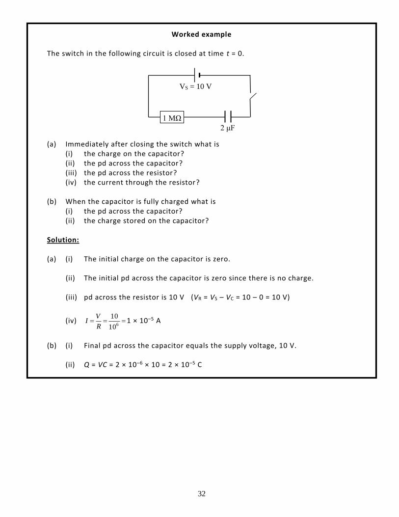
Worked example The switch in the following circuit is closed at time t = 0.
(a) Immediately after closing the switch what is (i) the charge on the capacitor? (ii) the pd across the capacitor? (iii) the pd across the resistor? (iv) the current through the resistor? (b) When the capacitor is fully charged what is (i) the pd across the capacitor? (ii) the charge stored on the capacitor? Solution: (a) (i) The initial charge on the capacitor is zero.
(ii) The initial pd across the capacitor is zero since there is no charge. (iii) pd across the resistor is 10 V (VR = VS – VC = 10 – 0 = 10 V)
(iv) 610
10
R
VI 1 × 10⁻⁵ A
(b) (i) Final pd across the capacitor equals the supply voltage, 10 V. (ii) Q = VC = 2 × 10–6 × 10 = 2 × 10⁻⁵ C
1 MΩ
VS = 10 V
2 μF
33
3.2 Electrons at Work Conductors, Semi conductors and Insulators
Classifying materials
By considering the electrical properties of materials, we can divide them into three groups:
Material Electrical properties
Conductor Materials with many free electrons. These electrons can easily be made to flow through the material. Examples: all metals, semi-metals like carbon- graphite, antimony and arsenic.
Insulator Materials that have very few free electrons. Examples: plastic, glass and wood.
Semi -conductor Materials that behave like insulators when pure, but will conduct when an impurity is added and/ or in response to light, heat, voltage etc. Examples: Elements: silicon, germanium, selenium Compounds: gallium arsenide and indium antimonide.
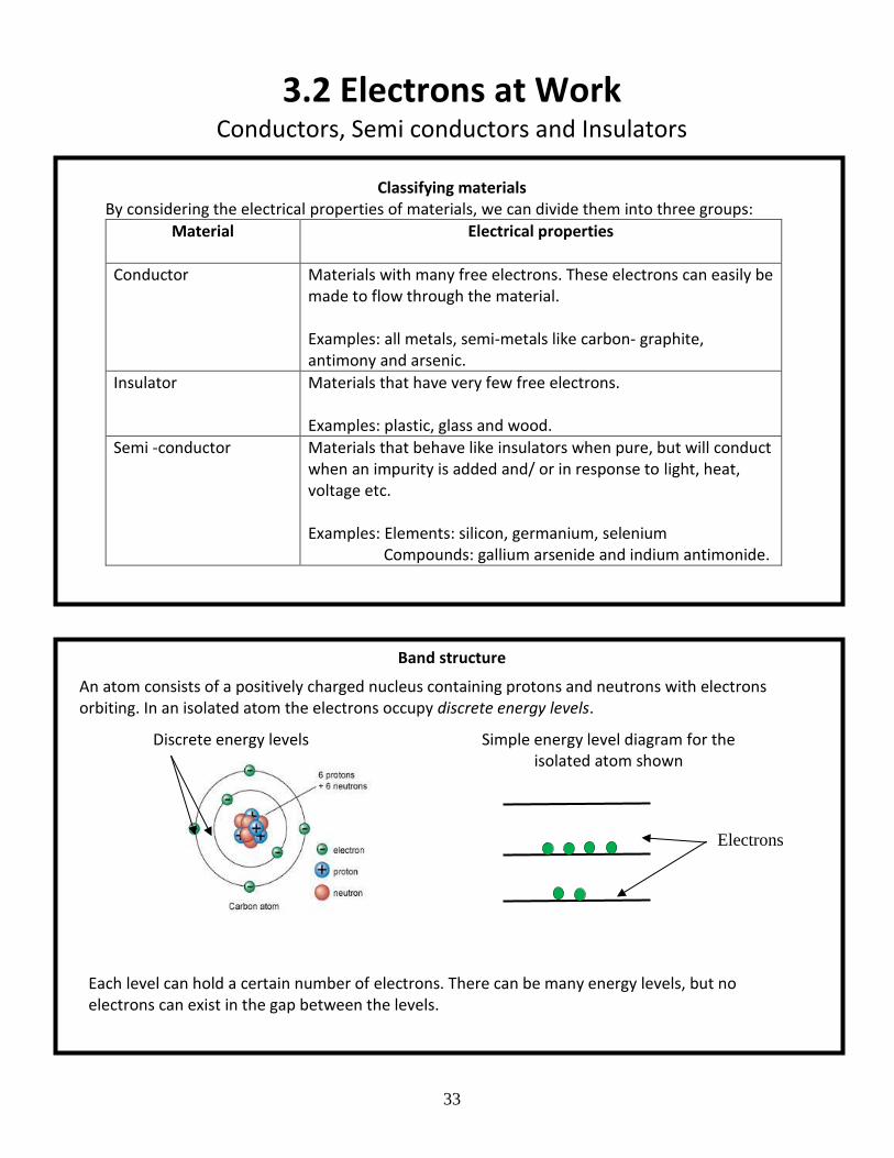
Band structure
An atom consists of a positively charged nucleus containing protons and neutrons with electrons orbiting. In an isolated atom the electrons occupy discrete energy levels.
Each level can hold a certain number of electrons. There can be many energy levels, but no electrons can exist in the gap between the levels.
Discrete energy levels
Electrons
Simple energy level diagram for the isolated atom shown
34
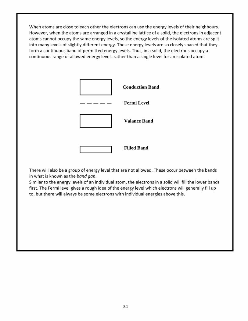
When atoms are close to each other the electrons can use the energy levels of their neighbours. However, when the atoms are arranged in a crystalline lattice of a solid, the electrons in adjacent atoms cannot occupy the same energy levels, so the energy levels of the isolated atoms are split into many levels of slightly different energy. These energy levels are so closely spaced that they form a continuous band of permitted energy levels. Thus, in a solid, the electrons occupy a continuous range of allowed energy levels rather than a single level for an isolated atom.
There will also be a group of energy level that are not allowed. These occur between the bands in what is known as the band gap. Similar to the energy levels of an individual atom, the electrons in a solid will fill the lower bands first. The Fermi level gives a rough idea of the energy level which electrons will generally fill up to, but there will always be some electrons with individual energies above this.
Conduction Band
Fermi Level
Valance Band
Filled Band
35
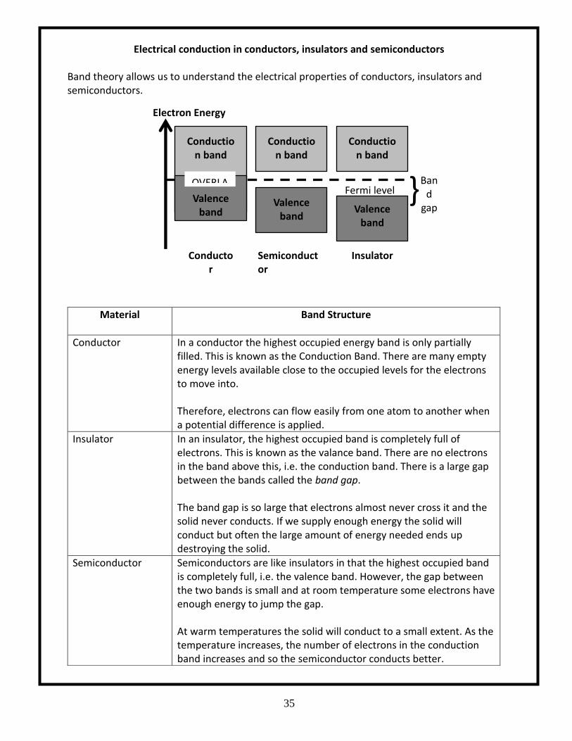
Electrical conduction in conductors, insulators and semiconductors
Band theory allows us to understand the electrical properties of conductors, insulators and
semiconductors.
Material Band Structure
Conductor In a conductor the highest occupied energy band is only partially filled. This is known as the Conduction Band. There are many empty energy levels available close to the occupied levels for the electrons to move into. Therefore, electrons can flow easily from one atom to another when a potential difference is applied.
Insulator In an insulator, the highest occupied band is completely full of electrons. This is known as the valance band. There are no electrons in the band above this, i.e. the conduction band. There is a large gap between the bands called the band gap. The band gap is so large that electrons almost never cross it and the solid never conducts. If we supply enough energy the solid will conduct but often the large amount of energy needed ends up destroying the solid.
Semiconductor Semiconductors are like insulators in that the highest occupied band is completely full, i.e. the valence band. However, the gap between the two bands is small and at room temperature some electrons have enough energy to jump the gap. At warm temperatures the solid will conduct to a small extent. As the temperature increases, the number of electrons in the conduction band increases and so the semiconductor conducts better.
Conductor
Insulator Semiconductor
Electron Energy
Conduction band
Conduction band
Conduction band
Valence band
Valence band
}
Band
gap
Fermi level Valence
band
OVERLA
36
Bonding in Semiconductors
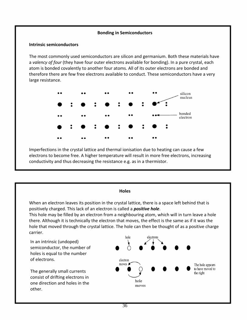
Intrinsic semiconductors The most commonly used semiconductors are silicon and germanium. Both these materials have a valency of four (they have four outer electrons available for bonding). In a pure crystal, each atom is bonded covalently to another four atoms. All of its outer electrons are bonded and therefore there are few free electrons available to conduct. These semiconductors have a very large resistance.
Imperfections in the crystal lattice and thermal ionisation due to heating can cause a few electrons to become free. A higher temperature will result in more free electrons, increasing conductivity and thus decreasing the resistance e.g. as in a thermistor.
Holes
When an electron leaves its position in the crystal lattice, there is a space left behind that is positively charged. This lack of an electron is called a positive hole. This hole may be filled by an electron from a neighbouring atom, which will in turn leave a hole there. Although it is technically the electron that moves, the effect is the same as if it was the hole that moved through the crystal lattice. The hole can then be thought of as a positive charge carrier.
p – n junctions
Doping
In an intrinsic (undoped) semiconductor, the number of holes is equal to the number of electrons. The generally small currents consist of drifting electrons in one direction and holes in the other.

37
p – n junctions
Doping The electrical properties of semiconductors make them very important in electronic devices such as transistors, diodes and light dependant resistors (LDRs). Doping is the addition of a very small amount of impurity e.g. arsenic, to a pure semiconductor. This action dramatically changes the electrical properties of a material, i.e. allows a semiconductor to conduct. Once doped these materials are known as extrinsic semiconductors.
n –type semiconductors
If an impurity such as arsenic (As), which has five outer electrons, is present in the crystal lattice, then four of its electrons will be used in bonding with the silicon. The fifth will be free to move about and conduct. Since the ability of the crystal to conduct is increased, the resistance of the semiconductor is therefore reduced.
This type of semiconductor is called n-type, since most conduction is by the movement of free electrons, which are negatively charged.
38
p –type semiconductors
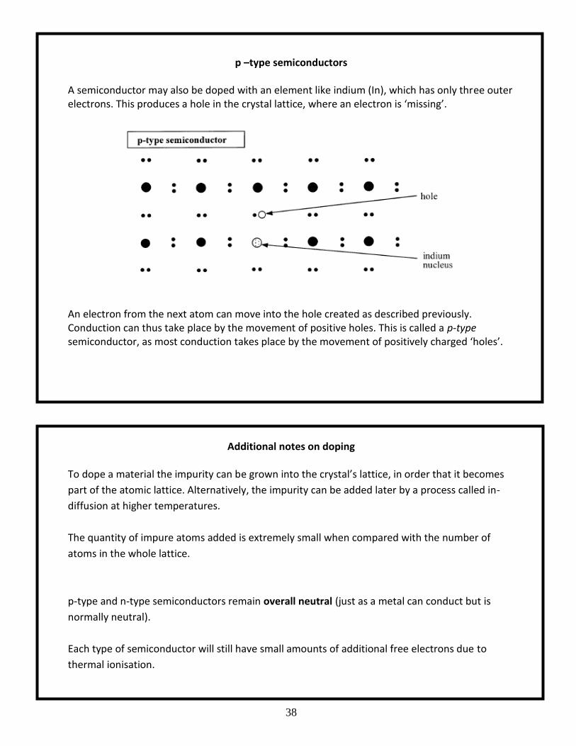
A semiconductor may also be doped with an element like indium (In), which has only three outer electrons. This produces a hole in the crystal lattice, where an electron is ‘missing’.
An electron from the next atom can move into the hole created as described previously. Conduction can thus take place by the movement of positive holes. This is called a p-type semiconductor, as most conduction takes place by the movement of positively charged ‘holes’.
Additional notes on doping
To dope a material the impurity can be grown into the crystal’s lattice, in order that it becomes
part of the atomic lattice. Alternatively, the impurity can be added later by a process called in-
diffusion at higher temperatures.
The quantity of impure atoms added is extremely small when compared with the number of
atoms in the whole lattice.
p-type and n-type semiconductors remain overall neutral (just as a metal can conduct but is
normally neutral).
Each type of semiconductor will still have small amounts of additional free electrons due to
thermal ionisation.

39
How doping affects Band Structure
In terms of band structure, we can represent the electrons as dots in the conduction band, and holes as circles in the valance band, as shown in the diagram below. The diagram also illustrates how the additional energy levels produced by the addition of the impure atoms changes the Fermi level (the top of the collection of electron energy levels at absolute zero) and make it easier for electrons to move up to the conduction band in n-type semiconductors and for holes to be created in the valance band of the p-type.
n –type semiconductor: extra electrons present, the Fermi level is closer to the conduction band. p – type semiconductor: fewer electrons present.
FERMI LEVEL
INCREASED
FERMI LEVEL
DECREASED
40
p –n junctions
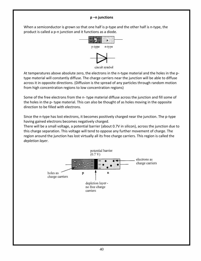
When a semiconductor is grown so that one half is p-type and the other half is n-type, the product is called a p-n junction and it functions as a diode.
At temperatures above absolute zero, the electrons in the n-type material and the holes in the p-type material will constantly diffuse. The charge carriers near the junction will be able to diffuse across it in opposite directions. (Diffusion is the spread of any particles through random motion from high concentration regions to low concentration regions) Some of the free electrons from the n- type material diffuse across the junction and fill some of the holes in the p- type material. This can also be thought of as holes moving in the opposite direction to be filled with electrons. Since the n-type has lost electrons, it becomes positively charged near the junction. The p-type having gained electrons becomes negatively charged. There will be a small voltage, a potential barrier (about 0.7V in silicon), across the junction due to this charge separation. This voltage will tend to oppose any further movement of charge. The region around the junction has lost virtually all its free charge carriers. This region is called the depletion layer.
41
p– n junctions: Band energy diagrams
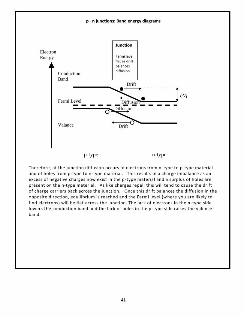
Therefore, at the junction diffusion occurs of electrons from n-type to p-type material and of holes from p-type to n-type material. This results in a charge imbalance as an excess of negative charges now exist in the p-type material and a surplus of holes are present on the n-type material. As like charges repel, this will tend to cause the drift of charge carriers back across the junction. Once this drift balances the diffusion in the opposite direction, equilibrium is reached and the Fermi level (where you are likely to find electrons) will be flat across the junction. The lack of electrons in the n-type side lowers the conduction band and the lack of holes in the p-type side raises the valence band.
Electron
Energy
Fermi Level
n-type p-type
Conduction
Band
Valance
Band
eVi
Drift
Drift
Diffusion
Diffusion
Junction Fermi level flat as drift balances diffusion
42
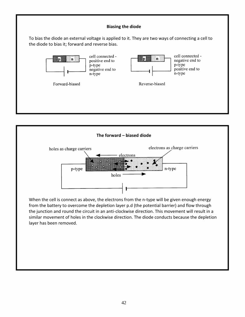
Biasing the diode
To bias the diode an external voltage is applied to it. They are two ways of connecting a cell to the diode to bias it; forward and reverse bias.
The forward – biased diode
When the cell is connect as above, the electrons from the n-type will be given enough energy from the battery to overcome the depletion layer p.d (the potential barrier) and flow through the junction and round the circuit in an anti-clockwise direction. This movement will result in a similar movement of holes in the clockwise direction. The diode conducts because the depletion layer has been removed.
43
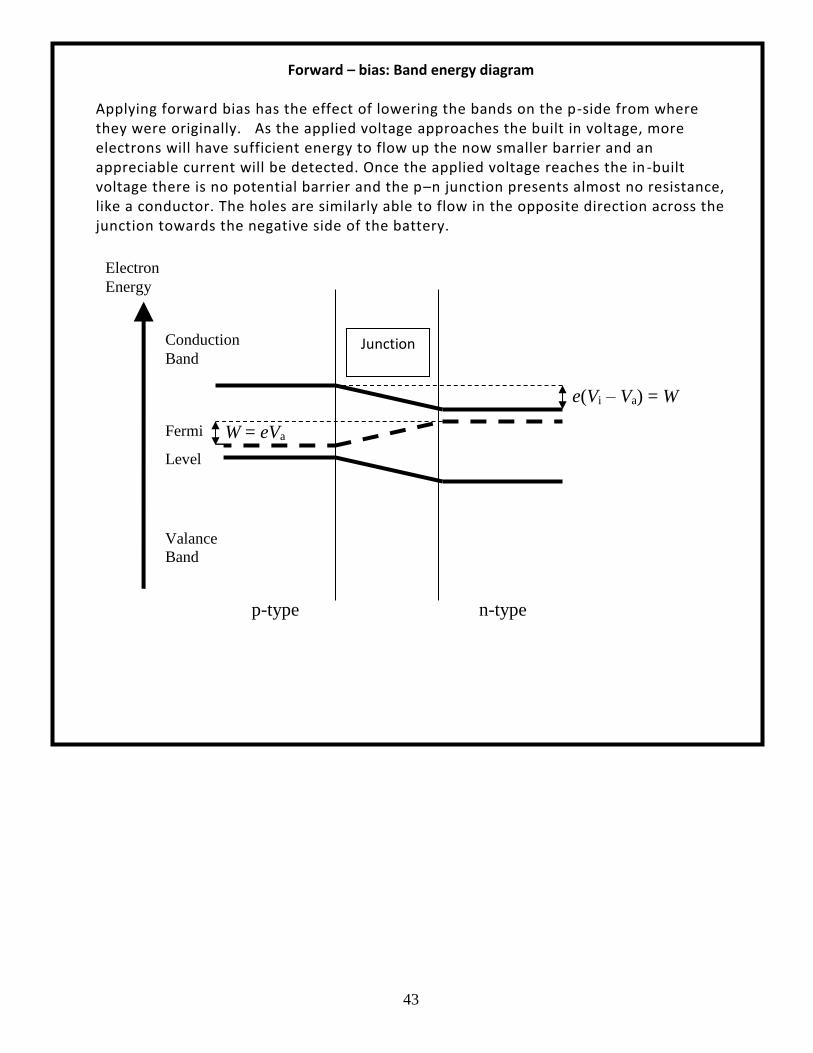
Forward – bias: Band energy diagram Applying forward bias has the effect of lowering the bands on the p-side from where they were originally. As the applied voltage approaches the built in voltage, more electrons will have sufficient energy to flow up the now smaller barrier and an appreciable current will be detected. Once the applied voltage reaches the in -built voltage there is no potential barrier and the p–n junction presents almost no resistance, like a conductor. The holes are similarly able to flow in the opposite direction across the junction towards the negative side of the battery.
Junction
Electron
Energy
Fermi
level
n-type p-type
Conduction
Band
Valance
Band
e(Vi – Va) = W
W = eVa
Level
44
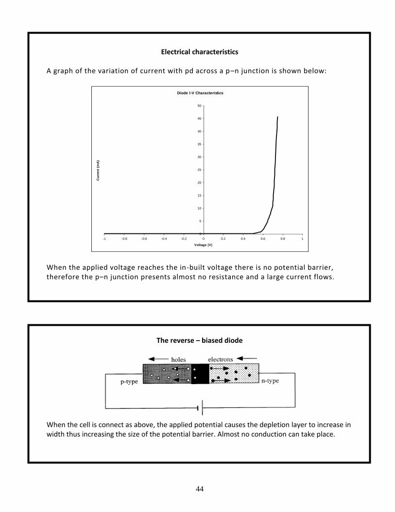
Electrical characteristics
A graph of the variation of current with pd across a p–n junction is shown below:
When the applied voltage reaches the in-built voltage there is no potential barrier, therefore the p–n junction presents almost no resistance and a large current flows.
The reverse – biased diode
When the cell is connect as above, the applied potential causes the depletion layer to increase in width thus increasing the size of the potential barrier. Almost no conduction can take place.
Diode I-V Characteristics
0
5
10
15
20
25
30
35
40
45
50
-1 -0.8 -0.6 -0.4 -0.2 0 0.2 0.4 0.6 0.8 1
Voltage (V)
Cu
rren
t (m
A)
45
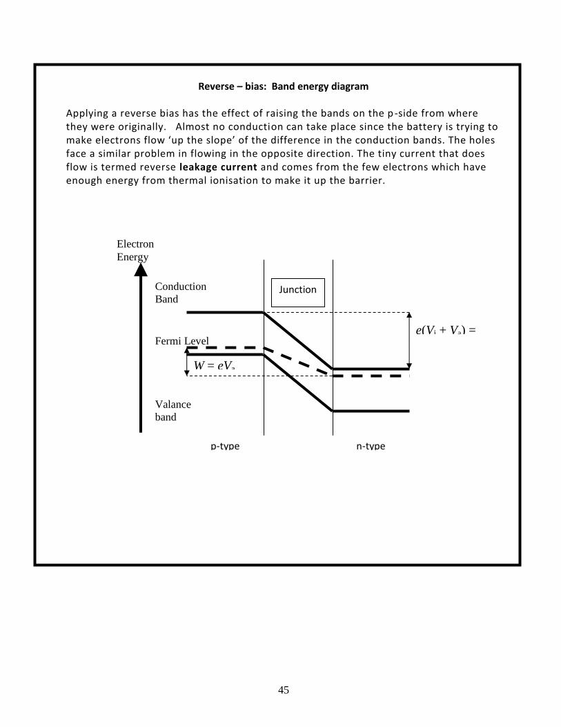
Reverse – bias: Band energy diagram
Applying a reverse bias has the effect of raising the bands on the p -side from where they were originally. Almost no conduction can take place since the battery is trying to make electrons flow ‘up the slope’ of the difference in the conduction bands. The holes face a similar problem in flowing in the opposite direction. The tiny current that does flow is termed reverse leakage current and comes from the few electrons which have enough energy from thermal ionisation to make it up the barrier.
Electron
Energy
Fermi Level
n-type p-type
Conduction
Band
Valance
band
e(Vi + Va) =
W
W = eVa
Junction

46
Current flow in p-n junctions
In conclusion, a p-n junction will only allow current to flow through it one way, as indicated below.
In practice, a very small current will flow in the opposite direction i.e. the leakage current. This is important in some applications such as a light dependant resistor.
The light emitting diode (LED)
One application of the p-n junction is the LED. An LED consists of a p-n junction diode connected to a positive and negative terminal. The junction is encased in a transparent plastic as shown below.
current flow
current flow
47
How does an LED work?
When the p-n junction is connected in forward bias, electrons and holes pass through the junction in opposite directions. Sometimes the holes and electrons will meet and recombine. When this happens energy is emitted in the form of a photon of radiation. For each recombination of electron and hole, one photon of radiation is emitted. Depending on the type of semiconductor used the radiation may be in the form of heat resulting in a temperature increase. However, in some semiconductors such as gallium arsenic phosphide, the energy is emitted as photons of light. The colour of the emitted light depends on the relative amounts of gallium, arsenic and phosphorous used to produce the semiconductor. The frequency of light from the LED’s is controlled by the size of the energy gap between the conduction and valence bands. A bigger gap will result in a larger energy change and a higher frequency of light will be emitted. The recombination energy can be calculated using E = h f, if the frequency is known. [As discussed previously, the diode does not conduct in reverse bias, therefore an LED will not work when connect in reverse bias.]
LED: worked example
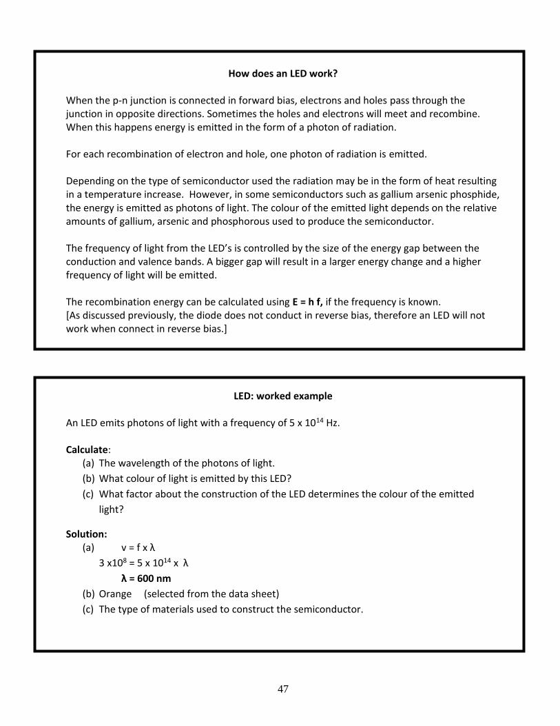
An LED emits photons of light with a frequency of 5 x 10¹⁴ Hz. Calculate:
(a) The wavelength of the photons of light.
(b) What colour of light is emitted by this LED?
(c) What factor about the construction of the LED determines the colour of the emitted
light?
Solution: (a) v = f x λ
3 x108 = 5 x 10¹⁴ x λ
λ = 600 nm
(b) Orange (selected from the data sheet)
(c) The type of materials used to construct the semiconductor.
48
The Photodiode
A p-n junction in a transparent coating will react to light due to the photoelectric effect.
The photodiode can be used in two modes; photovoltaic mode and photoconductive mode.
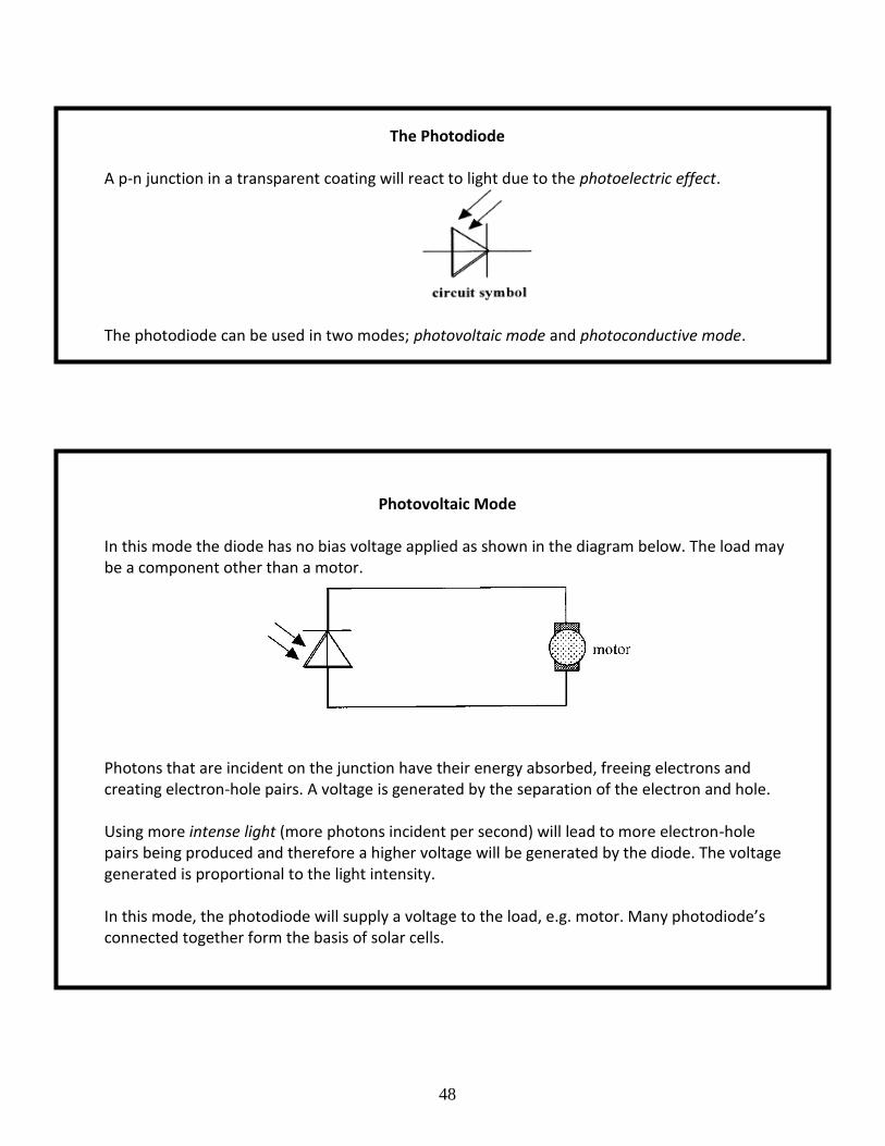
Photovoltaic Mode
In this mode the diode has no bias voltage applied as shown in the diagram below. The load may be a component other than a motor.
Photons that are incident on the junction have their energy absorbed, freeing electrons and creating electron-hole pairs. A voltage is generated by the separation of the electron and hole. Using more intense light (more photons incident per second) will lead to more electron-hole pairs being produced and therefore a higher voltage will be generated by the diode. The voltage generated is proportional to the light intensity. In this mode, the photodiode will supply a voltage to the load, e.g. motor. Many photodiode’s connected together form the basis of solar cells.
49
Photoconductive Mode
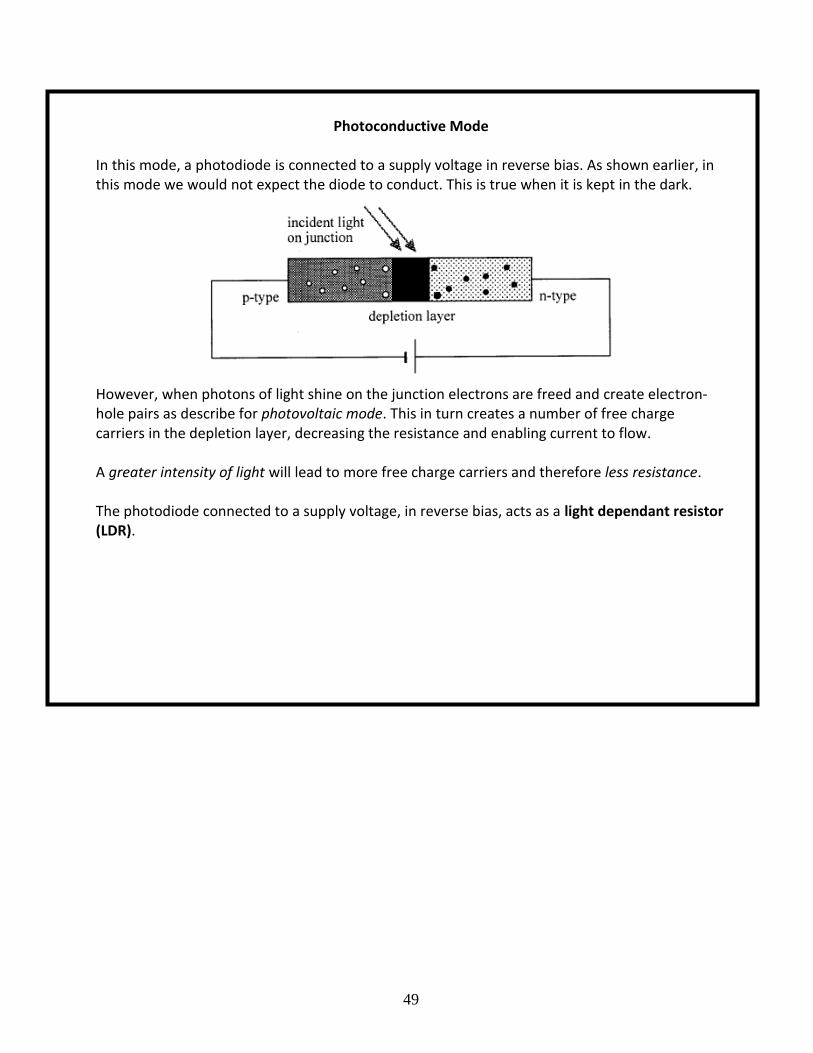
In this mode, a photodiode is connected to a supply voltage in reverse bias. As shown earlier, in this mode we would not expect the diode to conduct. This is true when it is kept in the dark.
However, when photons of light shine on the junction electrons are freed and create electron-hole pairs as describe for photovoltaic mode. This in turn creates a number of free charge carriers in the depletion layer, decreasing the resistance and enabling current to flow. A greater intensity of light will lead to more free charge carriers and therefore less resistance. The photodiode connected to a supply voltage, in reverse bias, acts as a light dependant resistor (LDR).


