Page 1
CHAPTER 1
INTRODUCTION
The knowledge behind the electric power generated by the direct conversion of solar
energy in the past was low simply because little attention was paid to what was space
technology, which was also utilising this solar energy conversion. But its potential is
gaining prominence and as a result, the physical processes involved are looked into.
Solar cells are basically solid-state (especially p-n diode) devices, which are made from
semiconductors. As such, the physics of the photovoltaic effect are linked with some
aspects of the semiconductor physics. The explanation used will be based on the classical
theory of a non-illuminated diode developed by Schottky and Spenke as the crystal
(material), the dopant and the junction are linked with the diode operation.
A quick look at the history shows that Becquerel first observed photovoltaic effect in an
electrolyte in 1839. This PV effect was then discovered in 1876, on a semiconductor
(selenium) by Adams and Day. But the PV effect could not be explained until in 1905,
when Einstein used the quantum theory developed by Planck. Light was regarded as
travelling in wave packets (photons), which upon striking a material will cause the
material to eject electrons. This, of course, could only take place if the photon energy
(which depends on the frequency) was high as some of its energy would be transferred to
the electrons. Many experiments were later conducted which led to the creation of solar
cells and were used in a satellite (VANGUARD) in 1958 and for terrestrial applications
such as navigation lights and communication stations in 1956.
Materials are classified as conductors (metals), insulators and semiconductors based on
their current capabilities. In a conductor, electrons in the outer shell (1 or 2) of an atom
Page 2
2
are always free to roam about and hence conduct electricity. The reverse is the case in an
insulator as the electrons in the outer shell (6 or 7) are held tightly to the atom and do not
conduct electricity. For a semiconductor, which is in between the conductor and the
insulator, it has some electrons that become loose and roam about once there is a
temperature increase. The fraction of electrons f, having energy equal to or greater than E
is f = exp ( - E / kT ). This is as a result of the average energy, known as the energy gap,
Eg, acquired allowing its conductivity to rise. The conductivities of these materials are
given below (Table 1.1).
Table 1.1. Conductivities of materials [2]
Material
Conductivity (Siemens/cm-1
)
Conductor
Insulator
Semiconductor
>106
< 10-10
10-8
– 102
Page 3
3
CHAPTER 2
SEMICONDUCTOR MATERIALS
Semiconductors exist in crystalline, polycrystalline or amorphous form. The table below
shows their atomic/molecular arrangement (Table 2.1).
Table 2.1. Arrangement of atoms/molecules in semiconductors
Crystalline
Polycrystalline
Amorphous
The atoms/molecules are
symmetrically arranged
and the array periodic
throughout the crystal
The atoms are also
symmetrically arranged but the
arrays are not well uniformed
with the atomic order and
regularity being totally
irregular
The atoms are not an
ordered array on any
macroscopic scale
Since silicon is very common element, focus will be given to their study. As the silicon
solar cells operate in the same way as other solar cells; they will be used as an example.
Pure, intrinsic silicon (i.e., silicon having the desired characteristic) has very little
impurities (the impurities have a concentration of less than 1018
m-3
) and electrical
resistivity ρ, of 2500 Ωm with four electrons at their outer shell, which have a covalent
bond with other neighbouring silicon atoms. As their crystals have different crystal
arrangements, their physical properties are not the same and as such affects the working
operation of the cells made from them. The properties of silicon can be looked in [2]. In a
Page 4
4
silicon crystal, each atom is equally spaced with four other atoms and all have four
electrons in their outer shells that are covalently bonded as seen in Figure 2.1.
Figure 2.1. Silicon at absolute zero (Source: Savant C. J. et al, (1991) Electronic Design: Circuits and
System, 2nd ed., The Benjamin/Cummings Company Inc., California)
At absolute zero, the crystal behaves like an insulator. In terms of energy bands, the
valence band is occupied by the electrons while the conduction band is completely
empty. As a result, since they cannot move to the conduction band, there is no change in
electrical conductivity. But if a strong external energy is applied, the electrons that are
covalently bonded acquire this energy and become free to move leaving in its initial
position a void, as the electron binding energy (forbidden energy band) is low. This void
(called a hole) assumes a positive charge and can be occupied by another electron from a
neighbouring silicon atom (Figure 2.2). This in turn creates another hole in the presence
of an electric field and we have equal number of electrons and holes.
Figure 2.2. Conduction from broken covalent bond (Source: Savant C. J. et al, (1991) Electronic Design:
Circuits and System, 2nd ed., The Benjamin/Cummings Company Inc., California)
Page 5
5
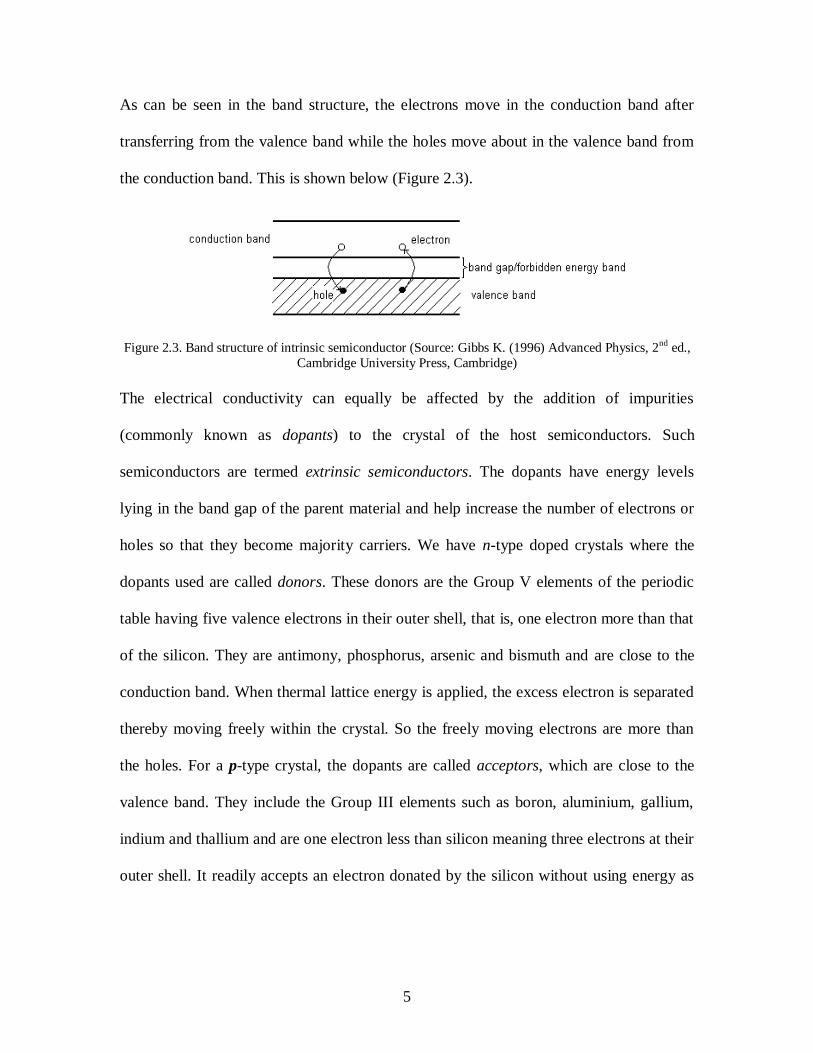
As can be seen in the band structure, the electrons move in the conduction band after
transferring from the valence band while the holes move about in the valence band from
the conduction band. This is shown below (Figure 2.3).
Figure 2.3. Band structure of intrinsic semiconductor (Source: Gibbs K. (1996) Advanced Physics, 2nd ed.,
Cambridge University Press, Cambridge)
The electrical conductivity can equally be affected by the addition of impurities
(commonly known as dopants) to the crystal of the host semiconductors. Such
semiconductors are termed extrinsic semiconductors. The dopants have energy levels
lying in the band gap of the parent material and help increase the number of electrons or
holes so that they become majority carriers. We have n-type doped crystals where the
dopants used are called donors. These donors are the Group V elements of the periodic
table having five valence electrons in their outer shell, that is, one electron more than that
of the silicon. They are antimony, phosphorus, arsenic and bismuth and are close to the
conduction band. When thermal lattice energy is applied, the excess electron is separated
thereby moving freely within the crystal. So the freely moving electrons are more than
the holes. For a p-type crystal, the dopants are called acceptors, which are close to the
valence band. They include the Group III elements such as boron, aluminium, gallium,
indium and thallium and are one electron less than silicon meaning three electrons at their
outer shell. It readily accepts an electron donated by the silicon without using energy as
Page 6
6
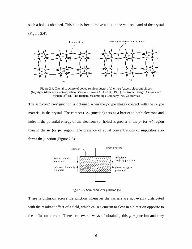
such a hole is obtained. This hole is free to move about in the valence band of the crystal
(Figure 2.4).
Figure 2.4. Crystal structure of doped semiconductors (a) n-type (excess electron) silicon
(b) p-type (deficient electron) silicon (Source: Savant C. J. et al, (1991) Electronic Design: Circuits and
System, 2nd ed., The Benjamin/Cummings Company Inc., California)
The semiconductor junction is obtained when the p-type makes contact with the n-type
material in the crystal. The contact (i.e., junction) acts as a barrier to both electrons and
holes if the potential energy of the electrons (or holes) is greater in the p- (or n-) region
than in the n- (or p-) region. The presence of equal concentrations of impurities also
forms the junction (Figure 2.5).
Figure 2.5. Semiconductor junction [5]
There is diffusion across the junction whenever the carriers are not evenly distributed
with the resultant effect of a field, which causes current to flow in a direction opposite to
the diffusion current. There are several ways of obtaining this p-n junction and they
Page 7
7
include: (a) ion implantation, (b) diffusion, (c) growing n-type impurity in p-type crystal
or vice versa, (d) alloy junction.
Page 8
8
CHAPTER 3
PHOTON ENERGY
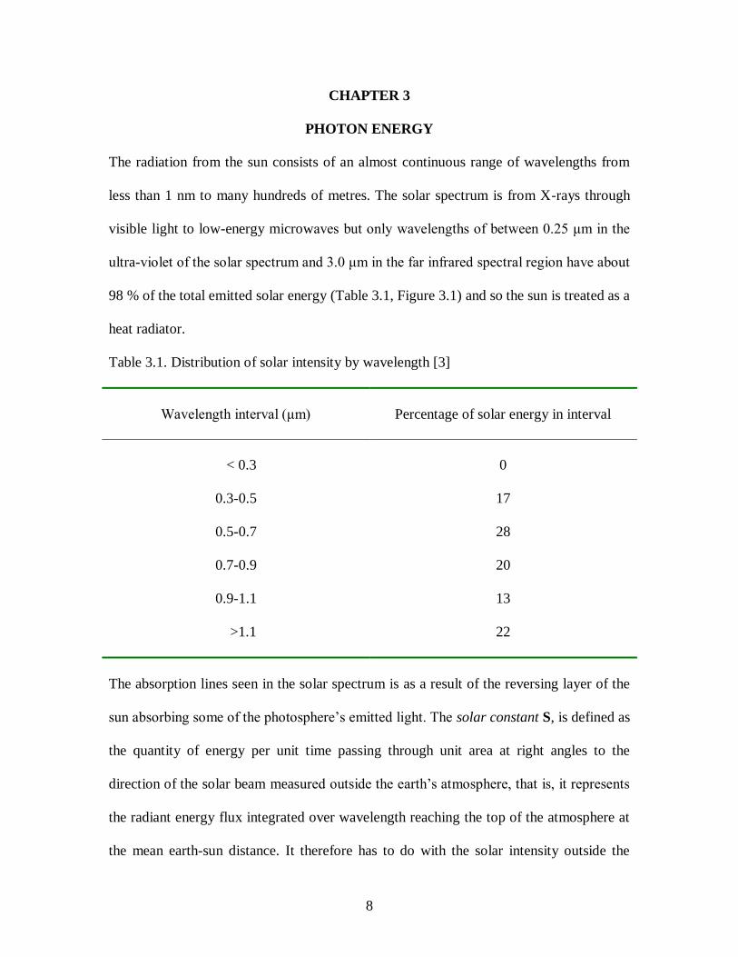
The radiation from the sun consists of an almost continuous range of wavelengths from
less than 1 nm to many hundreds of metres. The solar spectrum is from X-rays through
visible light to low-energy microwaves but only wavelengths of between 0.25 μm in the
ultra-violet of the solar spectrum and 3.0 μm in the far infrared spectral region have about
98 % of the total emitted solar energy (Table 3.1, Figure 3.1) and so the sun is treated as a
heat radiator.
Table 3.1. Distribution of solar intensity by wavelength [3]
Wavelength interval (μm)
Percentage of solar energy in interval
< 0.3
0.3-0.5
0.5-0.7
0.7-0.9
0.9-1.1
>1.1
0
17
28
20
13
22
The absorption lines seen in the solar spectrum is as a result of the reversing layer of the
sun absorbing some of the photosphere’s emitted light. The solar constant S, is defined as
the quantity of energy per unit time passing through unit area at right angles to the
direction of the solar beam measured outside the earth’s atmosphere, that is, it represents
the radiant energy flux integrated over wavelength reaching the top of the atmosphere at
the mean earth-sun distance. It therefore has to do with the solar intensity outside the
Page 9
9
earth’s atmosphere, which has a value of 1370 W/m2 (according to satellite
measurements).
Figure 3.1. Sensitivity range of silicon solar cells, compared with the solar spectrum outside the atmosphere
and at ground level [4]
The Air Mass is the changes in the sun’s beam path length as a result of the changes in
the sun’s zenith angle during the day. Therefore, Air Mass Zero (AM-0) means that when
the sun is at zenith the solar radiation is at sea level, which means the conditions are the
same to solar intensity of 1370 W/m2. A better way to put it, AM-0 is the solar light
outside the atmosphere. Its curve is called the solar spectral irradiance curve. The
Page 10
10
maximum light on the ground at sea level is called Air Mass One (AM-1) and its solar
intensity is nearly 1000 W/m2. In high mountains, the intensity increases to 1070 W/m
2
(Figure 3.2).
Figure 3.2. Relationship of air mass 1, 2 and 3 and declination is shown (Source: Hunt D. V. (1982) Solar
Energy Dictionary, Industrial Press Inc., New York)
Solar light consists of minute energy packet of electromagnetic radiation called photons
and the energy of a photon depends on radiation frequency. When an electron interacts
with light, it gains energy and this photon energy is given by Ef = hν where h is Planck’s
constant, which has a value of 6.63 x 10⁻³⁴
Js and ν is the light frequency. Once this
electron has this energy, which must be greater than the energy gap of the electron, it will
escape from the atom. This implies that the number of photons alongside with the solar
radiation energy must be known beforehand.
As a large portion of solar irradiance can be found in the far infra-red region, solar cells
cannot exploit the energy there as they are insensitive to that part of the solar spectrum
(as the crystal melts or the electrons will not be excited). Instead, the different spectral
Page 11
11
composition at sea level has the effect of concentrating more of the incoming energy in
the part of the spectrum where solar cells are sensitive (Figure 3.3).
Figure 3.3. Spectral response curve of a conventional silicon solar cell [4]
Page 12
12
CHAPTER 4
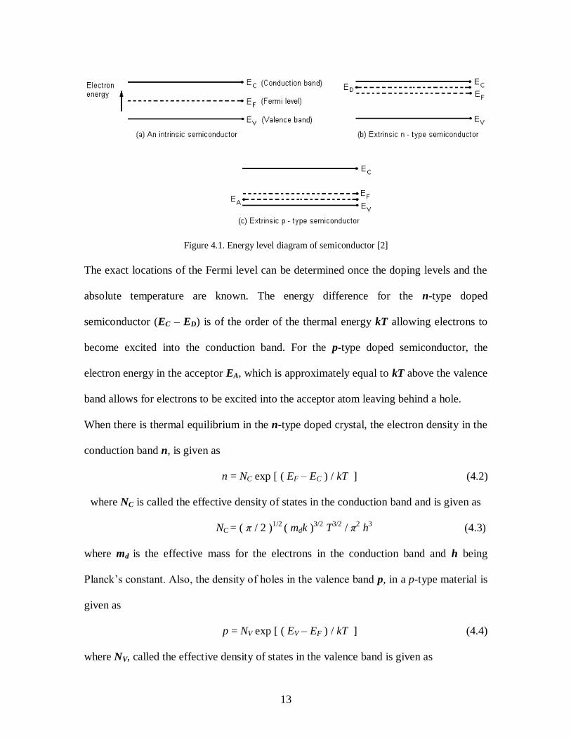
ELECTRON-HOLE CONCENTRATION AND FERMI LEVEL
Electrons are usually excited to higher state when they interact with phonons and
photons. But the number of electrons that can be allowed at any excited energy level is
determined by Pauli Exclusion Principle. This energy level is called the Fermi level. If
energy is given to electrons that is above the Fermi level, the distribution of electrons in
the allowed levels can be described using the Fermi-Dirac distribution function f ( E ),
given as
f (E) = 1 / { 1 + exp [ (E – EF ) / kT ] } (4.1)
where E is the energy of an allowed state, EF is the Fermi energy, k is Boltzmann’s
constant and T is the absolute temperature. At T = 0 K, f ( E ) = 1 up to an energy EF. The
Fermi level EF, is any energy level having the probability that is exactly one-half filled
with electrons. In an intrinsic (pure) semiconductor, the Fermi level is halfway in
between the energy gap, that is, EF = Eg / 2 so there are equal concentrations of electrons
and holes (Figure 4.1(a)). But for the extrinsic semiconductors, which have been doped,
the Fermi levels are in different positions, whether it is an n- or p-type doped crystal as
seen in Figures 4.1 (b) and 4.1 (c) respectively. For the n-type doped crystal, the Fermi
level is closer to the donor level ED while for the p-type doped crystal, the Fermi level is
closer to the acceptor level EA.
Page 13
13
Figure 4.1. Energy level diagram of semiconductor [2]
The exact locations of the Fermi level can be determined once the doping levels and the
absolute temperature are known. The energy difference for the n-type doped
semiconductor (EC – ED) is of the order of the thermal energy kT allowing electrons to
become excited into the conduction band. For the p-type doped semiconductor, the
electron energy in the acceptor EA, which is approximately equal to kT above the valence
band allows for electrons to be excited into the acceptor atom leaving behind a hole.
When there is thermal equilibrium in the n-type doped crystal, the electron density in the
conduction band n, is given as
n = NC exp [ ( EF – EC ) / kT ] (4.2)
where NC is called the effective density of states in the conduction band and is given as
NC = ( π / 2 )1/2
( mdk )3/2
T3/2
/ π2 h
3 (4.3)
where md is the effective mass for the electrons in the conduction band and h being
Planck’s constant. Also, the density of holes in the valence band p, in a p-type material is
given as
p = NV exp [ ( EV – EF ) / kT ] (4.4)
where NV, called the effective density of states in the valence band is given as
Page 14
14
NV = ( π / 2 )1/2
( mvk )3/2
T3/2
/ π2 h
3 (4.5)
where mv is the effective mass for the holes in the valence band.
For an intrinsic semiconductor, since there are no impurities present, the number of holes
and electrons is equal. It is this number per unit volume that is called the intrinsic carrier
concentration ni.
n = p = ni (4.6)
Therefore, the product of the number of holes and electrons is constant when the
semiconductor is in thermal equilibrium, that is,
np = ni2 = NC NV exp [ - ( EC – EV ) / kT ]
= NC NV exp [ - ( Eg ) / kT ] (4.7)
From equations (4.6) and (4.7), the Fermi energy level can be obtained as
EF = ( EC + EV ) / 2 + kT / 2 ln ( NV / NC ) (4.8)
The implication of the above equation is that the Fermi level is exactly halfway in
between the conduction and valence band once they have equal numbers of electrons and
holes and moves closer to either of the bands whenever the density of states rises or falls.
Since the total macroscopic change neutrality is neither altered nor affected by the
addition of impurities, it fulfils the following condition:
p – n = N -A – N
+D (4.9)
where N -A and N
+D are the ionised acceptor and donor atoms and are given as
N -A = NA / { 1 + exp [ (EA – EF ) / kT ] } (4.10)
and
N +
D = ND exp [ (ED – EF ) / kT ] / { 1 + exp [ (ED – EF ) / kT ] } (4.11)
Page 15
15
where EA, ED are the electron energies of the acceptor and donor atoms while NA, ND are
the acceptor and donor impurity concentrations respectively.
The presence of impurities allows for the determination of the Fermi level position using
equations (4.2) and (4.4). Therefore,
ND = n = NC exp [ ( EF – EC ) / kT ]
Then,
ND / NC = exp [ ( EF – EC ) / kT ]
ln ND / NC = [ ( EF – EC ) / kT ]
EF – EC = kT ln ( ND / NC ) (4.12)
and
NA = p = NV exp [ ( EV – EF ) / kT ]
EV – EF = kT ln ( NA / NV ) (4.13)
The number of charge carriers determines the electrical conductivity σ, and is given as
the sum of both hole and electron conductivities;
σ = σn + σp = q (n μn + p μp ) (4.14)
where q is the electronic charge and μn and μp are the electron and hole mobilities
respectively and is given as
μ = v / E (4.15)
where v is the charge carrier velocity and E is the applied field. In a semiconductor, the
electron or hole is always in random motion colliding with other atoms of both the
material and the impurity and other charge carriers. The mobility depends on the impurity
concentration and temperature if the electric field is small. This is because the mobility
reduces if the semiconductor is heavily doped.
Page 16
16
CHAPTER 5
A P-N JUNCTION
An n-type material is made to have contact with a p-type material forming the p-n
junction ( ) in a crystal. Prior to this formation, both materials are electrically
neutral. In the n-type material, the electrons diffuse to the p-type material through the
junction. This is as a result of a potential gradient. The diffusion current in, that results, is
then given as
in = q Dn dn / dx (5.1)
where x is the distance in the crystal and Dn is the diffusion constant, which is obtained
using the relation
Dn = μn kT / q (5.2)
Symmetrically, a diffusion current of holes ip, flows in the opposite direction;
ip = q Dp dp / dx (5.3)
Because of the diffusion of electrons to the p-type material, the n-type material is now
positively charged while the p-type material is negatively charged since there is a
deficiency of holes. As a result, we have an induced electric polarisation in an
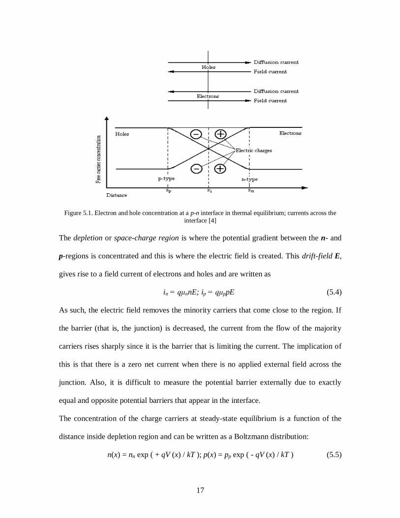
unilluminated p-n junction. The diffusion effect of the charge carriers is shown (Figure
5.1).
Page 17
17
Figure 5.1. Electron and hole concentration at a p-n interface in thermal equilibrium; currents across the
interface [4]
The depletion or space-charge region is where the potential gradient between the n- and
p-regions is concentrated and this is where the electric field is created. This drift-field E,
gives rise to a field current of electrons and holes and are written as
in = qμnnE; ip = qμppE (5.4)
As such, the electric field removes the minority carriers that come close to the region. If
the barrier (that is, the junction) is decreased, the current from the flow of the majority
carriers rises sharply since it is the barrier that is limiting the current. The implication of
this is that there is a zero net current when there is no applied external field across the
junction. Also, it is difficult to measure the potential barrier externally due to exactly
equal and opposite potential barriers that appear in the interface.
The concentration of the charge carriers at steady-state equilibrium is a function of the
distance inside depletion region and can be written as a Boltzmann distribution:
n(x) = nn exp ( + qV (x) / kT ); p(x) = pp exp ( - qV (x) / kT ) (5.5)
Page 18
18
where nn, pp are the electron and hole equilibrium concentrations in the n- and p-layers, V
(x) the junction built-in electric potential and n, p the charge carrier concentrations.
The diffusion voltage VD, is defined as the total voltage across the junction usually of the
order of 1 V and is bigger than the photovoltage as seen later.
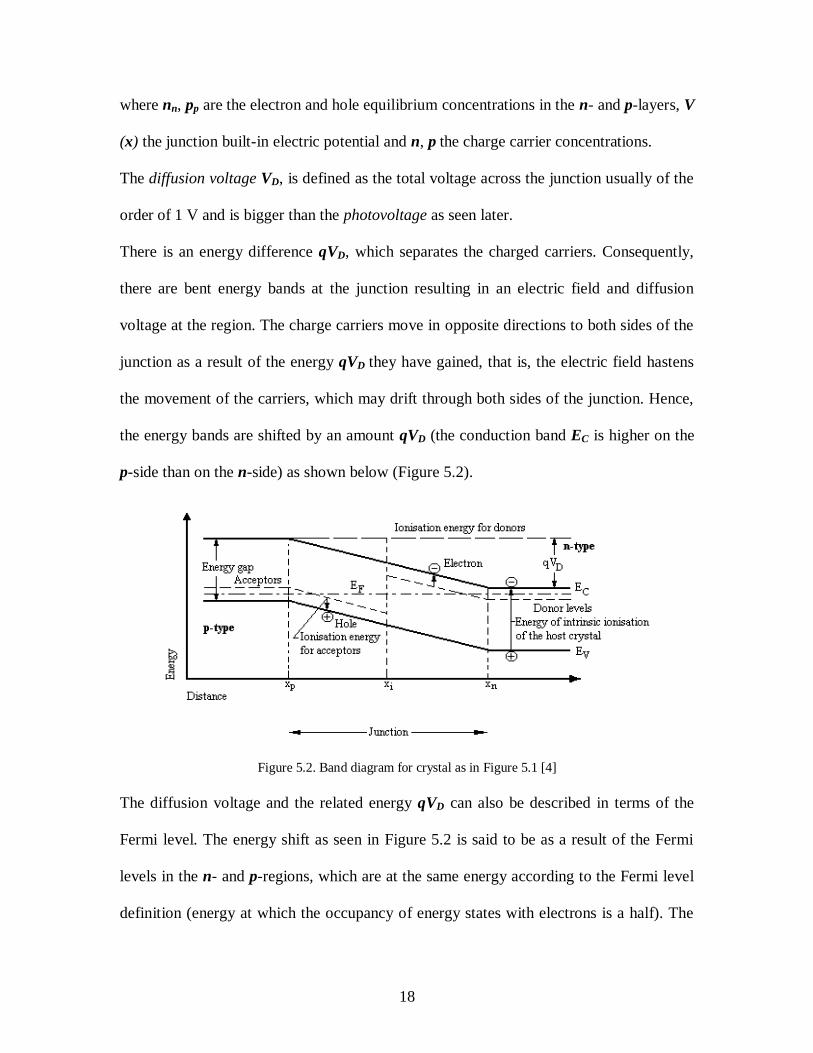
There is an energy difference qVD, which separates the charged carriers. Consequently,
there are bent energy bands at the junction resulting in an electric field and diffusion
voltage at the region. The charge carriers move in opposite directions to both sides of the
junction as a result of the energy qVD they have gained, that is, the electric field hastens
the movement of the carriers, which may drift through both sides of the junction. Hence,
the energy bands are shifted by an amount qVD (the conduction band EC is higher on the
p-side than on the n-side) as shown below (Figure 5.2).
Figure 5.2. Band diagram for crystal as in Figure 5.1 [4]
The diffusion voltage and the related energy qVD can also be described in terms of the
Fermi level. The energy shift as seen in Figure 5.2 is said to be as a result of the Fermi
levels in the n- and p-regions, which are at the same energy according to the Fermi level
definition (energy at which the occupancy of energy states with electrons is a half). The
Page 19
19
electrons move from the valence band to the conduction band due to thermal energy and
so we have more carriers above (for the electrons) and below (for the holes) the Fermi
level whenever there is an increase in the temperature. The Fermi level is closer to the
conduction band for an n-type material (with donors) that has a high concentration of
electrons while the Fermi level is closer to the valence band for a p-type material since
the amount of electrons in it is low. This can be seen in Figure 5.2. Above a certain
temperature, the Fermi level lies between the n- and the p-layer since more electrons
become thermally ionised from the valence band to the conduction band. This is a
consequence of the intrinsic transitions where the crystal behaves as if it is not doped and
so the junction disappears since there is an equal amount of electrons in the conduction
band. The photovoltage then vanishes when the crystal is under light.
At thermal equilibrium, the rate at which electrons are occupied at any given energy must
be equal throughout the material. Therefore, thermal equilibrium means homogeneous
Fermi level. This thermal equilibrium can be disrupted once a voltage or light is applied.
A charge dipole is created near the junction as a result of the field caused by the electrons
in the p-type material. So in thermal equilibrium there is no net current flow and therefore
no energy in the dipole, only a voltage.
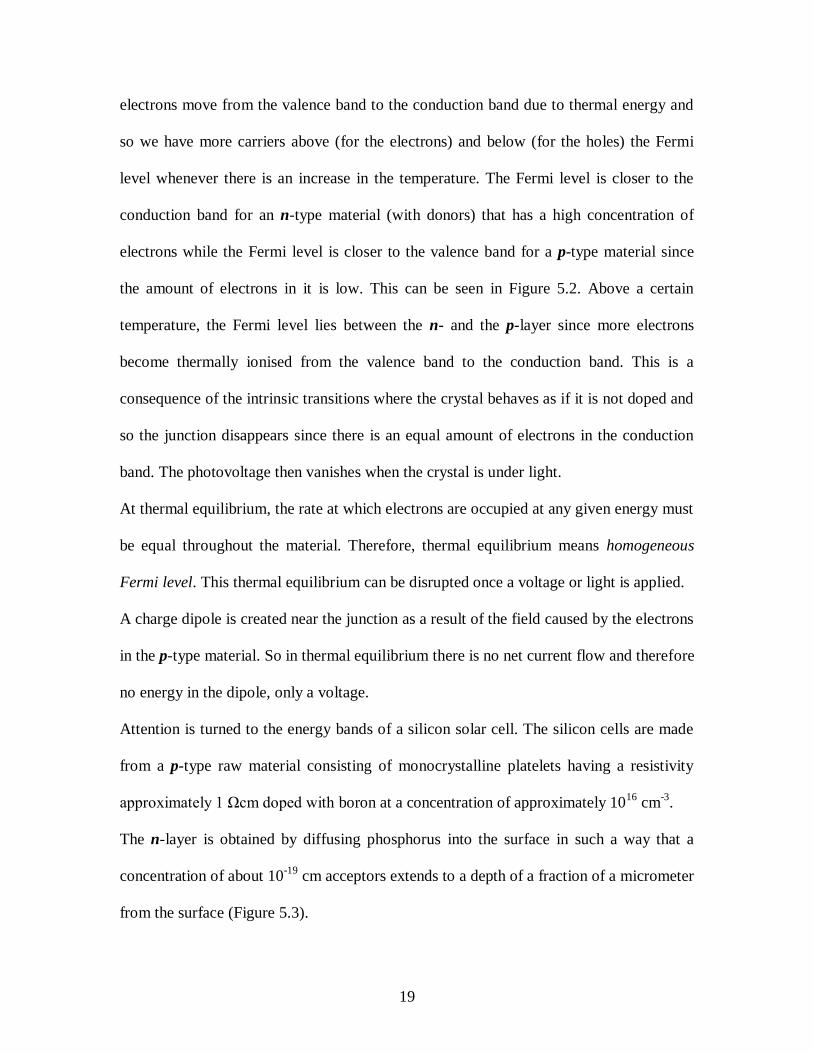
Attention is turned to the energy bands of a silicon solar cell. The silicon cells are made
from a p-type raw material consisting of monocrystalline platelets having a resistivity
approximately 1 Ωcm doped with boron at a concentration of approximately 1016
cm-3
.
The n-layer is obtained by diffusing phosphorus into the surface in such a way that a
concentration of about 10-19
cm acceptors extends to a depth of a fraction of a micrometer
from the surface (Figure 5.3).
Page 20
20
Figure 5.3. Schematic cross-section of conventional silicon solar cell [4]
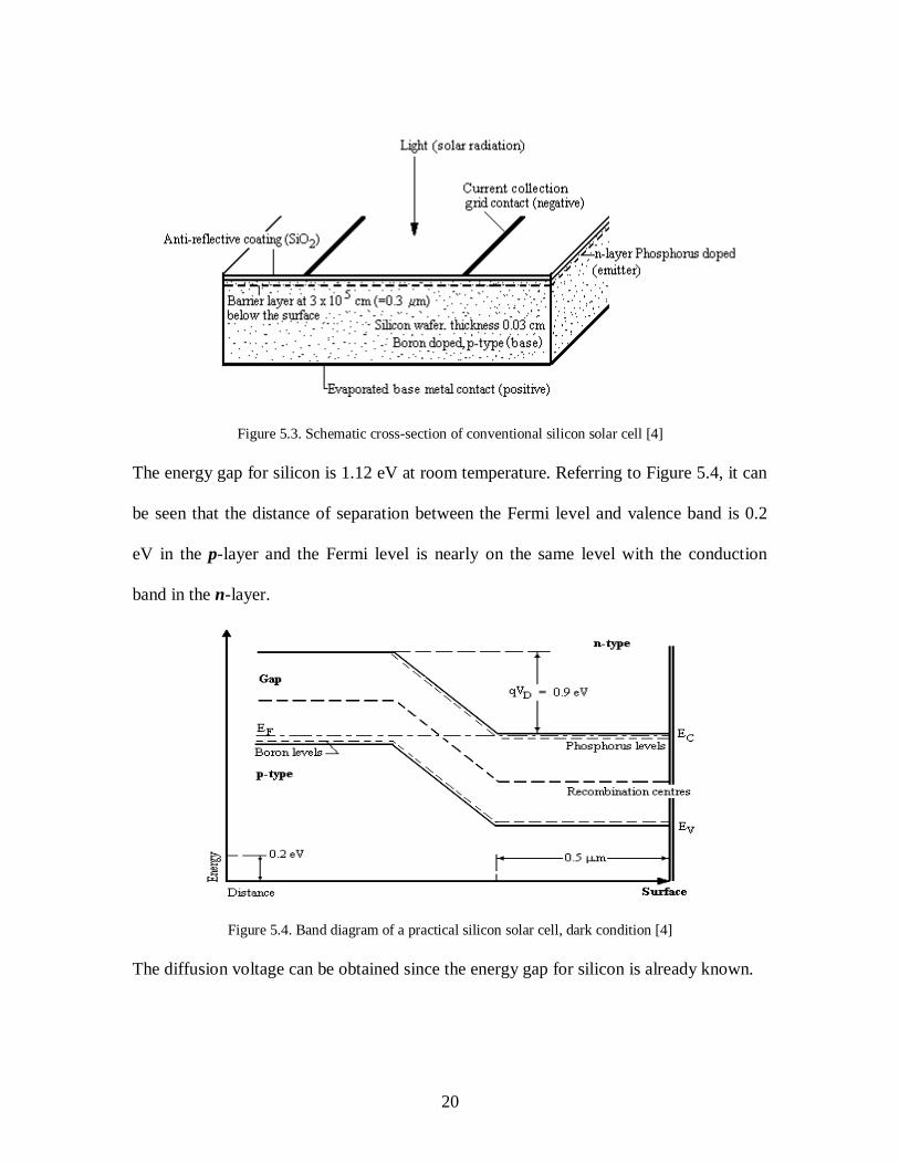
The energy gap for silicon is 1.12 eV at room temperature. Referring to Figure 5.4, it can
be seen that the distance of separation between the Fermi level and valence band is 0.2
eV in the p-layer and the Fermi level is nearly on the same level with the conduction
band in the n-layer.
Figure 5.4. Band diagram of a practical silicon solar cell, dark condition [4]
The diffusion voltage can be obtained since the energy gap for silicon is already known.
Page 21
21
The value is nearly 0.9 eV (= 1.12 – 0.2 eV) at room temperature and is the photovoltage
upper limit.
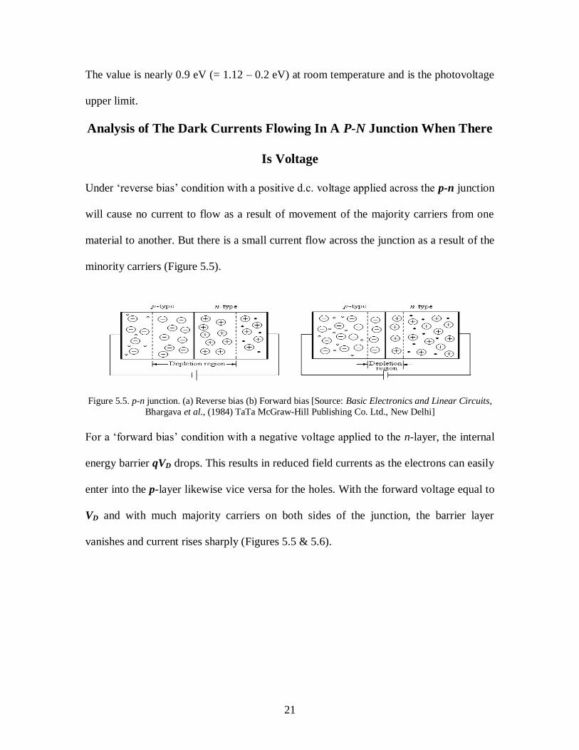
Analysis of The Dark Currents Flowing In A P-N Junction When There
Is Voltage
Under ‘reverse bias’ condition with a positive d.c. voltage applied across the p-n junction
will cause no current to flow as a result of movement of the majority carriers from one
material to another. But there is a small current flow across the junction as a result of the
minority carriers (Figure 5.5).
Figure 5.5. p-n junction. (a) Reverse bias (b) Forward bias [Source: Basic Electronics and Linear Circuits,
Bhargava et al., (1984) TaTa McGraw-Hill Publishing Co. Ltd., New Delhi]
For a ‘forward bias’ condition with a negative voltage applied to the n-layer, the internal
energy barrier qVD drops. This results in reduced field currents as the electrons can easily
enter into the p-layer likewise vice versa for the holes. With the forward voltage equal to
VD and with much majority carriers on both sides of the junction, the barrier layer
vanishes and current rises sharply (Figures 5.5 & 5.6).
Page 22
22
Figure 5.6. Band diagram of a practical silicon cell in the dark with a voltage of 0.5 V applied to the n-layer
(forward characteristic) [4]
The electron and hole currents can be described using Figures 5.1 & 5.3. At the point of
contact xi, the value of the electric current is the same as that of the hole current that is if
there is an equal amount of doping in both n- and p- materials of the crystal. Using the
Boltzmann distribution, at the point xn, the low concentration of holes at equilibrium is
given as
p(xn) = pn = pp exp ( - qVD / kT ) (5.6)
This concentration changes once there is an applied voltage VF. Thus,
p(xn)F = pp exp { - ( q [ VD - VF ] / kT ) } = pn exp ( qVF / kT ) (5.7)
The excess holes p(xn)F – p(xn) diffuses into the n- layer some distance and recombine
with electrons in the crystal defects or with metal ions of the n-material. This distance is
proportional to the diffusion constant Dp, measured cm2s
-1, and the lifetime of the holes
τp, which is defined as the times needed for the number of holes to decay to 1/ exp of the
previous values (here, it is assumed high). The average distance that the holes travel
before it is recombines is called the diffusion length Lp. As a result, the excess holes
concentration decays exponentially and the decay as a function of the distance from xn
can be written as
Page 23
23
p(x)F = pn { exp ( qV / kT ) }{ exp ( - [ x - xp ] / Lp ) } (5.8)
Likewise, at xp of the p-layer, the decay of excess electrons concentration can also be
written as
n(x)F = np { exp ( qV / kT ) }{ exp ( - [ xn - x ] / Ln ) } (5.9)
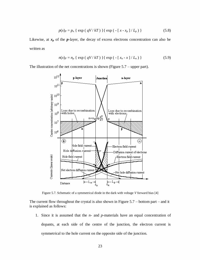
The illustration of the net concentrations is shown (Figure 5.7 – upper part).
Figure 5.7. Schematic of a symmetrical diode in the dark with voltage V forward bias [4]
The current flow throughout the crystal is also shown in Figure 5.7 – bottom part – and it
is explained as follows:
1. Since it is assumed that the n- and p-materials have an equal concentration of
dopants, at each side of the centre of the junction, the electron current is
symmetrical to the hole current on the opposite side of the junction.
Page 24
24
2. There is a diffusion current flow into the layers at xp and when there is an increase
in the applied voltage, the diffusion current rises exponentially. This current is the
limiting process for the current flow through the crystal.
3. Inside the layers is a field current that reduces towards the junction.
4. Inside the junction, the field and diffusion currents have higher values than in the
layers. The effective voltage in the junction is VD – Vapplied. Therefore, the field
current in the junction flows in the opposite direction to that in the layers, where
the applied voltage is ε x Vapplied (ε << 1).
The current-voltage (I-V) characteristic equation can then be derived based on the
schematic description of the diode currents. The diffusion current is written as
ip = - q Dp dpF / dx (5.10)
dpF / dx is derived using equation (5.8) and this is given as
dp(x)F / dx = - ( 1 / Lp ) pn { exp ( qV / kT ) }{ exp ( - [ x - xp ] / Lp ) }
dp(x)F / dx = - ( 1 / Lp ) p(x)F (5.11)
Therefore, the diffusion current can be rewritten as
ip = ( q Dp / Lp ) p(x)F (5.12)
In the n-layer, the amount of holes fed into it can be written as
p(x)F = p(x) – pn (5.13)
where p(x) is the total concentration and pn the concentration of holes in the n-layer in
thermal equilibrium. At xn, we have
ip(xp) = ( q Dp / Lp ) ( p(x) – pn ) (5.14)
Using equation (5.7), ip(xp) can be rewritten as
ip(xp) = ( q Dp / Lp ) pn { exp ( qVF / kT ) - pn }
Page 25
25
= ( q Dp / Lp ) { exp ( qVF / kT ) - 1 } pn (5.15)
Since xp is symmetrical to xn, in is then given as
in(xn) = ( q Dn / Ln ) { exp ( qVF / kT ) - 1 }np (5.16)
ip(xp) = ip(xn) when it crosses the junction since only a very small number of holes are
lost. So also, in(xn) = in(xp) as there is no reduction when it crosses the junction. The total
current for a biased diode can then be computed as either ip(xp) + in(xn) or ip(xn) + in(xp),
which gives
iF = q [ (Dp pn / Lp ) + ( Dn np / Ln ) ] { exp ( qVF / kT ) - 1 } (5.17)
(adding equations (5.15) and (5.16)). The first term is called the saturation (or dark)
current:
iS = q [ (Dp pn/ Lp ) + ( Dn np/ Ln ) ] (5.18)
This saturation current, therefore, depends on the diffusion of the minority carriers. The
values of np and pn can be obtained using the expressions
np = ni2 / Np = ni
2 / p; pn = ni
2 / Nn = ni
2 / n (5.19)
Dp = ( kT / q ) μp; Dn = ( kT / q ) μn (5.20)
Equation (5.20) is the Einstein relations. Lp and Ln are also obtained using the
expressions
Lp = (Dp τp)½; Ln = (Dn τn)
½ (5.21)
So the saturation current can be rewritten as
iS = q [ pn (Dp / τp )½
+ np (Dn / τn )½
] (5.22)
It is, thus, a function of equilibrium densities of carriers, diffusion rates and carrier
lifetimes. Going back to equation (5.17), it is then rewritten as
Page 26
26
iF = iS { exp ( qVF / kT ) - 1 } (5.23)
iF, which is the total current can equally be called the junction current or better still the
diode current under forward bias. So in all, because of the junction solar cells have diode
characteristics in the dark and this is important for the photovoltaic effect.
Some considerations have to be taken into cognisance when dealing with the practical
aspect such as the assumption that recombination is small everywhere in the crystal
which may not necessarily be so. It has been observed that, particularly within the space
region, recombination centres might have some effect on the current. As a result, the
recombination current as calculated by Shockley is given as
iR = iRO [ exp ( qVF / AkT ) – 1 ] (5.24)
where A is a constant.
Attention is now directed towards what happens when light is focussed on the p-n
junction.
The photovoltaic effect is responsible for the photocurrent generated by the solar cells.
When light is made to fall upon the semiconductor junction, each photon with EF > Eg
(as a result of internal ionisation) can cause one minority and one majority carrier to be
produced as electron-hole pairs in either of the two regions. The concentration of the
electrons and holes depends on the light absorption rate and the carrier lifetime.
Equilibrium is attained in the flow of both the majority and minority carriers as a result of
the decrease in the potential barrier caused by some of the minority carriers that have
been swept across the junction. With this decrease, the potential barrier (in volts) can be
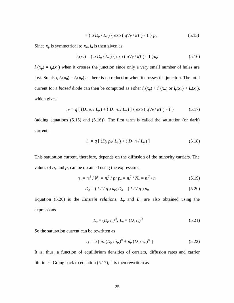
measured externally as seen in Figure 5.8 (a).
Page 27
27
(a) without external load (b) with external load
Figure 5.8. Solar cell equivalent [5]
In Figure 5.8 (a), the current in the diode IJ, is equal to the added photon-generated
minority carrier current Iph, so that
Iph = IJ (5.25)
If a load resistor is connected in parallel with the diode junction as in Figure 5.8 (b), the
photon-generated current Iph, will be divided between the diode and the resistor. The
electric current I, in the load resistor will be the difference between the diode current IJ,
and the photon-generated current Iph
Iph = IJ + ( - I (RL) ) (5.26)
(the minus sign indicates flow in the opposite direction).
I (RL) = IJ - Iph
= IS { exp ( qVF / kT ) - 1 } - Iph (5.27)
This is for an idealised solar cell. With the recombination current given from equation
(5.24), the electric current becomes
I (RL) = IS { exp ( qVF / kT ) - 1 } + IRO [ exp ( qVF / AkT ) – 1 ] - Iph (5.28)
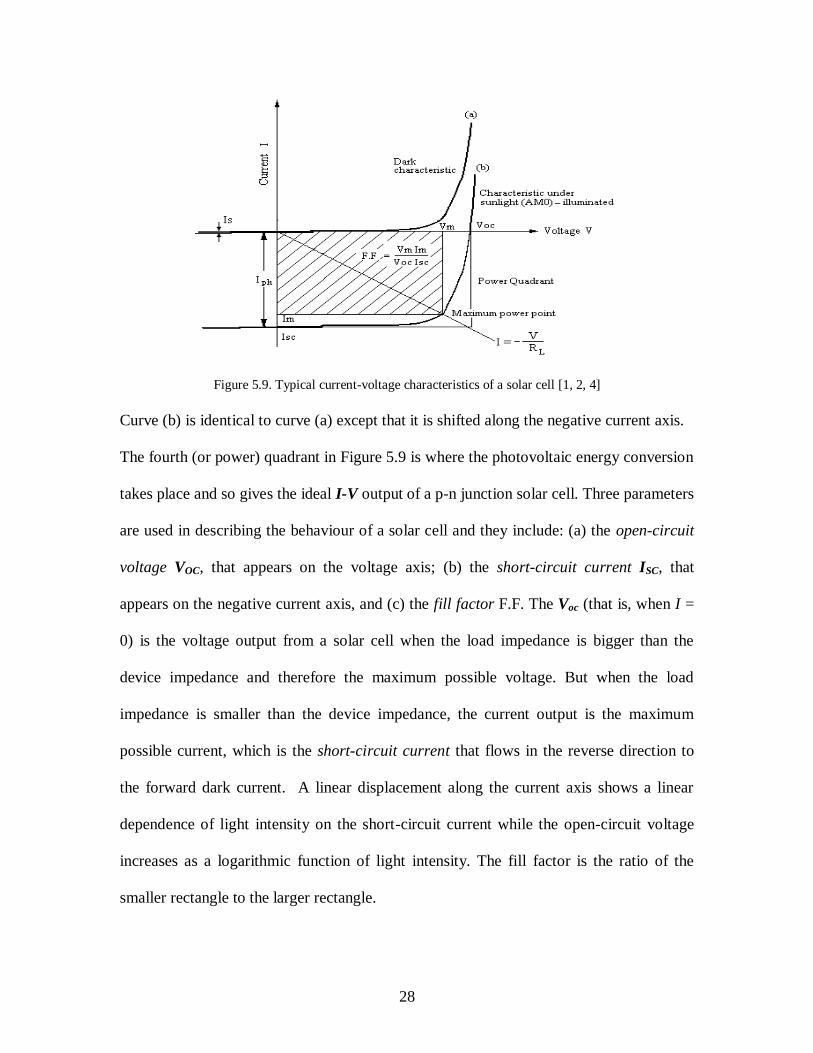
By varying the load resistance between zero and infinity, the current-voltage I-V,
characteristic of the solar cell may be gotten. For a p-n junction not illuminated, the I-V
characteristic is that as shown as curve (a) in Figure 5.9. Curve (b) is for an illuminated
p-n junction.
Page 28
28
Figure 5.9. Typical current-voltage characteristics of a solar cell [1, 2, 4]
Curve (b) is identical to curve (a) except that it is shifted along the negative current axis.
The fourth (or power) quadrant in Figure 5.9 is where the photovoltaic energy conversion
takes place and so gives the ideal I-V output of a p-n junction solar cell. Three parameters
are used in describing the behaviour of a solar cell and they include: (a) the open-circuit
voltage VOC, that appears on the voltage axis; (b) the short-circuit current ISC, that
appears on the negative current axis, and (c) the fill factor F.F. The Voc (that is, when I =
0) is the voltage output from a solar cell when the load impedance is bigger than the
device impedance and therefore the maximum possible voltage. But when the load
impedance is smaller than the device impedance, the current output is the maximum
possible current, which is the short-circuit current that flows in the reverse direction to
the forward dark current. A linear displacement along the current axis shows a linear
dependence of light intensity on the short-circuit current while the open-circuit voltage
increases as a logarithmic function of light intensity. The fill factor is the ratio of the
smaller rectangle to the larger rectangle.
Page 29
29
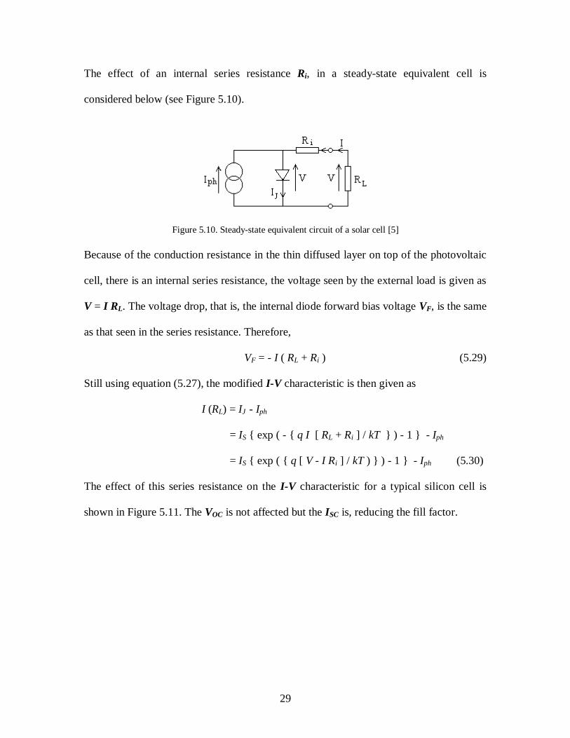
The effect of an internal series resistance Ri, in a steady-state equivalent cell is
considered below (see Figure 5.10).
Figure 5.10. Steady-state equivalent circuit of a solar cell [5]
Because of the conduction resistance in the thin diffused layer on top of the photovoltaic
cell, there is an internal series resistance, the voltage seen by the external load is given as
V = I RL. The voltage drop, that is, the internal diode forward bias voltage VF, is the same
as that seen in the series resistance. Therefore,
VF = - I ( RL + Ri ) (5.29)
Still using equation (5.27), the modified I-V characteristic is then given as
I (RL) = IJ - Iph
= IS { exp ( - { q I [ RL + Ri ] / kT } ) - 1 } - Iph
= IS { exp ( { q [ V - I Ri ] / kT ) } ) - 1 } - Iph (5.30)
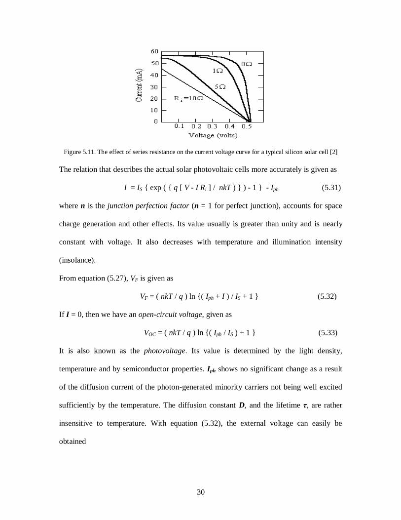
The effect of this series resistance on the I-V characteristic for a typical silicon cell is
shown in Figure 5.11. The VOC is not affected but the ISC is, reducing the fill factor.
Page 30
30
Figure 5.11. The effect of series resistance on the current voltage curve for a typical silicon solar cell [2]
The relation that describes the actual solar photovoltaic cells more accurately is given as
I = IS { exp ( { q [ V - I Ri ] / nkT ) } ) - 1 } - Iph (5.31)
where n is the junction perfection factor (n = 1 for perfect junction), accounts for space
charge generation and other effects. Its value usually is greater than unity and is nearly
constant with voltage. It also decreases with temperature and illumination intensity
(insolance).
From equation (5.27), VF is given as
VF = ( nkT / q ) ln {( Iph + I ) / IS + 1 } (5.32)
If I = 0, then we have an open-circuit voltage, given as
VOC = ( nkT / q ) ln {( Iph / IS ) + 1 } (5.33)
It is also known as the photovoltage. Its value is determined by the light density,
temperature and by semiconductor properties. Iph shows no significant change as a result
of the diffusion current of the photon-generated minority carriers not being well excited
sufficiently by the temperature. The diffusion constant D, and the lifetime τ, are rather
insensitive to temperature. With equation (5.32), the external voltage can easily be
obtained
Page 31
31
- I [ RL + Ri ] = ( nkT / q ) ln {( Iph + I ) / IS + 1 }
- I = ( nkT / q ) [ RL + Ri ]-1
ln {( Iph + I ) / IS + 1 }
Since V = - IRL, then
V / RL = ( nkT / q ) [ RL + Ri ]-1
ln {( Iph + I ) / IS + 1 }
V = ( nkT / q ) [ ( RL / RL + Ri ) ] ln {( Iph + I ) / IS + 1 }
= ( nkT / q ) [ ( 1 + Ri / RL ) ]-1
ln {( Iph + I ) / IS + 1 } (5.34)
The short-circuit current, that is, when V = 0 is given as the relation, using equation
(5.31)
ISC = IS { exp ( - qIRi / nkT ) - 1 } - Iph (5.35)
It can be seen then that ISC depends on the spectral response of the photovoltaic cell and
light spectrum. This spectral response also depends on some parameters such as the
optical absorption coefficient α, junction depth between xp and xn, depletion region width
W, lifetimes and mobilities of both sides of the junction, surface recombination velocity
s, the presence and absence of electric field.
For high quality cells, Ri can be removed or made small by metallisation of the material.
It then follows that ISC ≈ Iph. While the VOC is a strong function of temperature, the ISC is
not so dependent on the operating temperature as will be seen below.
The ISC can be interrelated with VOC. From equation (5.33)
Iph = IS { exp ( qVoc / kT ) - 1 } (5.36)
Substituting equation (5.36) into equation (5.35), we have
ISC = IS { exp ( qVoc / kT ) - exp ( - qIRi / kT ) } (5.37)
If Ri is made small for a good quality cell, then
ISC = IS { exp ( qVoc / kT ) - 1 } (5.38)
Page 32
32
The ISC can equally be written as
ISC = Ac T γ
exp ( - Ego / kT ) exp ( qVoc / kT ) (5.39)
where Ac is the area, Eg0 is the band gap at zero temperature, T, the temperature and γ
determines the temperature dependence of other terms determining IS, which lies between
1 and 4. The temperature rate of change of VOC can be determined using equation (5.39).
From equation (5.39)
VOC = Eg0 / q + kT / q ln ( ISC / Ac T γ ) (5.40)
dVOC / dT = k / q ln ( ISC / Ac T γ ) - γ k / q
= k / q { ln ( ISC / Ac T γ ) - γ } (5.41)
From equation (5.40)
ln ( ISC / Ac T γ ) = ( - Eg0 + q VOC ) / q (5.42)
Therefore,
dVOC / dT = k / q [ { ( q VOC - Eg0 ) / kT } - γ ]
= {VOC - Vg0 - ( kT / q ) } / T (5.43)
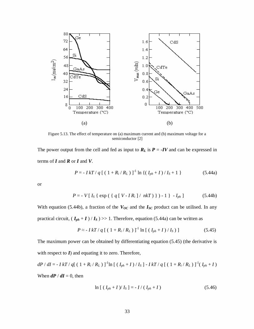
where Vg0 = Eg0 / q. It can therefore be deduced from equation (5.43) that an increase in
temperature results in a linear decrease in VOC. This is as a result, say, in silicon solar
cell, of the electron concentration n(xp), which balances the photon-generated current in
open-circuit condition as it depends exponentially on qVOC / kT. By allowing VOC to be
proportional to kT, that is, temperature, it is the only way to keep n(xp) constant. The
figure below (Figure 5.13 (a)) shows the temperature effect on maximum current Im, for
various semiconductors while Figure 5.13 (b) shows that on maximum voltage Vm.
Page 33
33
(a) (b)
Figure 5.13. The effect of temperature on (a) maximum current and (b) maximum voltage for a
semiconductor [2]
The power output from the cell and fed as input to RL is P = -IV and can be expressed in
terms of I and R or I and V.
P = - I kT / q [ ( 1 + Ri / RL ) ]-1
ln {( Iph + I ) / IS + 1 } (5.44a)
or
P = - V [ IS { exp ( { q [ V - I Ri ] / nkT ) } ) - 1 } - Iph ] (5.44b)
With equation (5.44b), a fraction of the VOC and the ISC product can be utilised. In any
practical circuit, ( Iph + I ) / IS ) >> 1. Therefore, equation (5.44a) can be written as
P ≈ - I kT / q [ ( 1 + Ri / RL ) ]-1
ln [ ( Iph + I ) / IS ) ] (5.45)
The maximum power can be obtained by differentiating equation (5.45) (the derivative is
with respect to I) and equating it to zero. Therefore,
dP / dI = - I kT / q[ ( 1 + Ri / RL ) ]-1
ln [ ( Iph + I ) / IS ] - I kT / q [ ( 1 + Ri / RL ) ]-1
( Iph + I )
When dP / dI = 0, then
ln [ ( Iph + I )/ IS ] = - I / ( Iph + I ) (5.46)
Page 34
34
This is a transcendental equation giving I in terms of Iph and IS. Equation (5.46) in
equation (5.45) gives the maximum available power from the solar cell as
Pmax = - Im kT / q [ ( 1 + Ri / RL ) ]-1
{ - Im / ( Iph + Im ) }
= kT / q [ ( 1 + Ri / RL ) ]-1
{ - Im / ( Iph + Im ) }(- Im )
Pm = Vm Im (5.47)
The efficiency of excited electrons collected determines the value of the maximum
current as it is less than ISC while the maximum voltage, which would be the voltage
across the load would probably be less than VOC / 2. This would give the power output as
nearly 32 % of the ideal value (48 %) as we shall see.
The fill factor (F.F.) can now be defined as the ratio of the maximum power to the
theoretical limit, that is, VOC and ISC product (Figure 5.9).
F.F. = Pm / VOC ISC (5.48)
which means the junction perfection factor and the series resistance are independent of
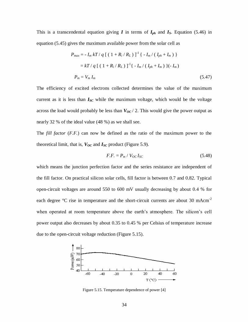
the fill factor. On practical silicon solar cells, fill factor is between 0.7 and 0.82. Typical
open-circuit voltages are around 550 to 600 mV usually decreasing by about 0.4 % for
each degree °C rise in temperature and the short-circuit currents are about 30 mAcm-2
when operated at room temperature above the earth’s atmosphere. The silicon’s cell
power output also decreases by about 0.35 to 0.45 % per Celsius of temperature increase
due to the open-circuit voltage reduction (Figure 5.15).
Figure 5.15. Temperature dependence of power [4]
Page 35
35
The efficiency η, of a solar cell is defined as the percentage of power supplied (when
electrical energy is converted from optical energy) and absorbed, when a solar cell is
connected to an electrical circuit. It is therefore the ratio between the electric power
obtained from the maximum power point of the I-V curve and the incident light.
η = Pm / Pin = ImVm / EAC (5.49)
where E is the input light irradiance under ‘standard’ test (AM-1.5) conditions measured
in W/m2 and AC the solar cell surface area. E is calculated using the expression
E = ∫0 ∞ ( hc / λ ) f ( λ ) d λ (5.50)
where f ( λ ) is the number of photons per square meter per second per unit bandwidth
incident on the cell surface at wavelength λ, hc / λ is the photon energy. Substitution of
equations (5.48) and (5.50) into equation (5.49) gives efficiency as
η = ( F.F. VOC ISC ) / [ AC ∫0 ∞ ( hc / λ ) f ( λ ) d λ ] (5.51)
It can equally be expressed in terms of mean number of carriers collected and mean
number of photons in the spectrum, given as
η = Q (Im / Isc )( Vm q nph(Eg) / Nph Eav ) ( Aa / AC ) ( 1 – R ) (5.52)
where Q is the mean collection efficiency given as the ratio of number of carriers
collected to Nph (Eg), nph (Eg) is the number of photons having energy greater than Eg per
square cm per second, R is the average reflectivity, Eav the mean photon energy, Aa the
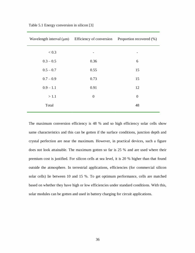
active area, AC the total device area. The table below (Table 5.1) shows the maximum
possible energy conversion in silicon at each wavelength.
Page 36
36
Table 5.1 Energy conversion in silicon [3]
Wavelength interval (μm)
Efficiency of conversion
Proportion recovered (%)
< 0.3
0.3 – 0.5
0.5 – 0.7
0.7 – 0.9
0.9 – 1.1
> 1.1
Total
-
0.36
0.55
0.73
0.91
0
-
6
15
15
12
0
48
The maximum conversion efficiency is 48 % and so high efficiency solar cells show
same characteristics and this can be gotten if the surface conditions, junction depth and
crystal perfection are near the maximum. However, in practical devices, such a figure
does not look attainable. The maximum gotten so far is 25 % and are used where their
premium cost is justified. For silicon cells at sea level, it is 20 % higher than that found
outside the atmosphere. In terrestrial applications, efficiencies (for commercial silicon
solar cells) lie between 10 and 15 %. To get optimum performance, cells are matched
based on whether they have high or low efficiencies under standard conditions. With this,
solar modules can be gotten and used in battery charging for circuit applications.
Page 37
37
CHAPTER 6
ABSORPTION IN A SEMICONDUCTOR
The absorption of light in a semiconductor is a function of wavelength of light and is
possible only if the wavelength is shorter than the absorption edge of the material under
light. It is expressed as
f ( λ, x ) = f0 ( λ ) exp ( - α( λ ) x ) (6.1)
where f ( λ, x ) is the photon flux, measured in mW/cm2 or photons per square cm per
second, f0 ( λ ) is the photon flux at x = 0 and α ( λ ) is the absorption coefficient. For an
electron to move from the valence band to the conduction band, the photon provides the
minimum energy at the absorption edge. There are two kinds of intrinsic absorption
observed in semiconductors; direct absorption and indirect absorption. As a result we
have the direct band-gap and indirect band-gap semiconductor.
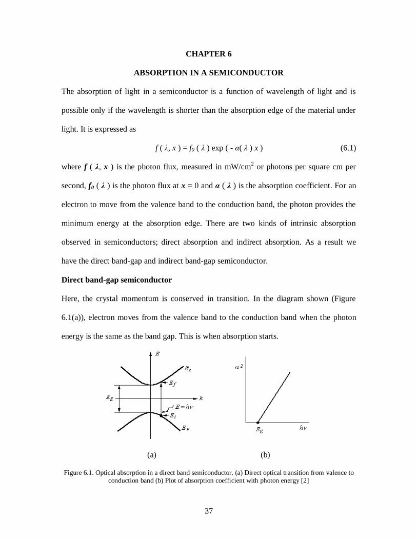
Direct band-gap semiconductor
Here, the crystal momentum is conserved in transition. In the diagram shown (Figure
6.1(a)), electron moves from the valence band to the conduction band when the photon
energy is the same as the band gap. This is when absorption starts.
(a) (b)
Figure 6.1. Optical absorption in a direct band semiconductor. (a) Direct optical transition from valence to
conduction band (b) Plot of absorption coefficient with photon energy [2]
Page 38
38
The absorption coefficient α, near the minimum energy for absorption band gap is given
as
α = ( 3.38 x 10⁷ / n ) ( me / mo )
1/2 ( Eg / hυ ) ( hυ - Eg )
1/2 (6.2)
where n is the index of refraction, mo is the free electron mass, me is the mass of electron.
( 3.38 x 10⁷ / n ) ( Eg / hυ ) is for allowed transitions while with forbidden transitions, the
absorption coefficient is given as
α = f (E) ( hυ - Eg ) 1/2
(6.3)
where f (E) is a function of energy. The plot of equation (6.3) is given in Figure 6.1(b).
The momentum of the photon is negligible and they include GaAs, GaN, CdS, CdTe,
CdSe, CuInSe2, Sn (grey), InAs, InSb, InN, ZnS, ZnO, S, Te, etc.
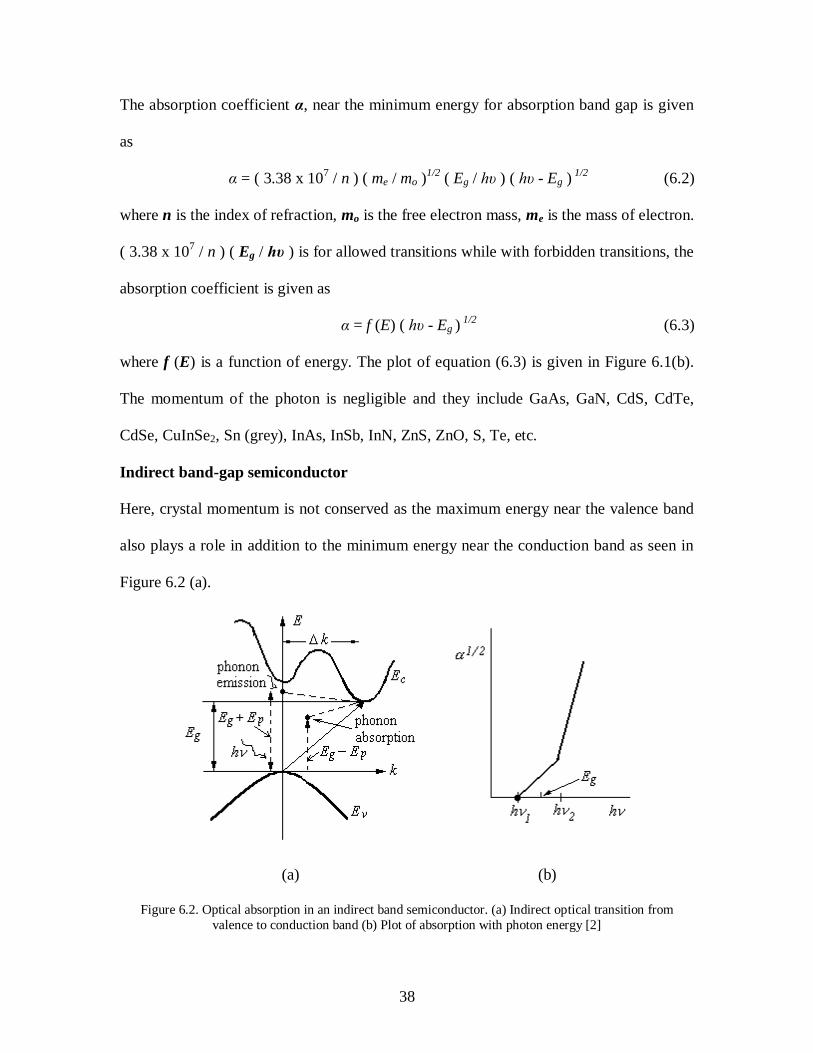
Indirect band-gap semiconductor
Here, crystal momentum is not conserved as the maximum energy near the valence band
also plays a role in addition to the minimum energy near the conduction band as seen in
Figure 6.2 (a).
(a) (b)
Figure 6.2. Optical absorption in an indirect band semiconductor. (a) Indirect optical transition from
valence to conduction band (b) Plot of absorption with photon energy [2]
Page 39
39
The process that happens in the direct band-gap semiconductor equally occurs here but in
a different manner. Here a phonon must be absorbed before transition can take place and
so
hν + Ep = Eg (6.4)
The minimum photon energy is therefore
hν = Eg - Ep (6.5)
where Ep is the absorbed phonon energy. The phonons have a high momentum but low
energy as compared with the photons. The absorption coefficient is given as
α = αa + αe (6.6)
where αa is due to phonon absorption while αe is the contribution due to phonon emission.
Both tend to zero if in the former hν < Eg - Ep and in the latter if hν < Eg + Ep. αa and αe
can be determined from these relations:
αa = A [ hν – ( Eg – Ep ) ]2 / [ exp ( Ep / kT ) – 1 ] (6.7a)
and
αe = A [ hν – ( Eg + Ep ) ]2 / [ 1– exp ( - Ep / kT ) ] (6.7b)
where A is a constant. For forbidden indirect transitions
α = f ( E, T ) [ hν – ( Eg – Ep ) ]2 (6.8)
where f ( E, T ) is a function of energy and temperature. With these, carriers gain more
energy than they have at thermal equilibrium. Compared to the direct band-gap, α is low.
Figure 6.2 (b) shows a plot of α1/2
and hν. The lower line intercepting at hν1 corresponds
to phonon absorption while the upper line intercepting at hν2 corresponds to phonon
emission. With this, the band gap and phonon energy can be written as
Eg = h ( ν1 + ν2 ) / 2; Ep = h ( ν1 - ν2 ) / 2 (6.9)
Page 40
40
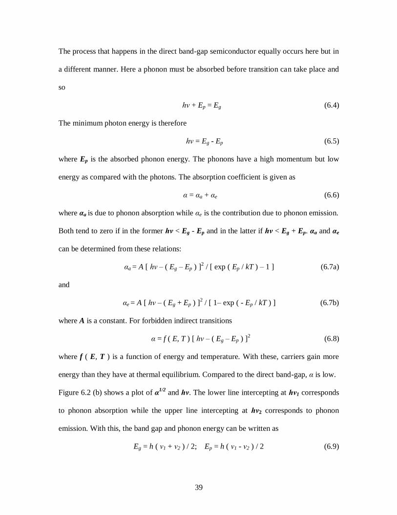
Examples of indirect band-gap semiconductor include Si, SiC, BaSi2, BeTe, AlAs, InP,
GaInAs, GaP, Ge, C (diamond), Se, etc. The optical absorption coefficient as a function
of photon energy is shown below (Figure 6.3).
Figure 6.3. Optical absorption coefficient as a function of photon energy for some semiconductors [2]
If the indirect band-gap material is used for solar cells, a very thick material is needed to
absorb most of the solar spectrum, as the absorption coefficient is inversely proportional
to the penetration depth of light. A thin direct gap material can equally be used though
they suffer from higher surface recombination losses.
In general, not every photon is able to produce an electron. The fraction of effective
photons is known as the quantum efficiency ηq, that is, it is an electron-hole pair that must
be produced from an incident photon. It is can be used in calculating the current, which is
given as
I = q ηq A Φbackground (6.10)
where Φbackground is the photon flux density, given in photons per second per square
centimetre, A is the junction area, and q is the electric charge respectively. The
expression A Φbackground is the light intensity H. So equation 6.10 can be rewritten as
Page 41
41
I = q ηq H (6.11)
For a p-n junction, the charge carriers created within the depletion region are directly
exposed to the strong field and this allows the carriers not to follow the mobility relation
μ = v / E. The strong field is given as VD / W where VD is the diffusion voltage and W is
the barrier width. The reason is that, in a strong field, interaction takes place between
electrons and optical phonons of the semiconductor lattice. Because the field current in
the junction is constant, it does not vary with voltage. This is the reason photon-generated
current remains constant irrespective of the applied voltage value to the solar cell
provided it is lower than VD. The photon-generated current is restricted to one side of the
junction for a direct band-gap semiconductor.
Page 42
42
CHAPTER 7
COMPARATIVE ANALYSIS OF SOLAR CELLS
The saturation current IS, can be written as a function of temperature. It is given as
IS = aT3 [ exp (– qEg / kT ) ] (7.1)
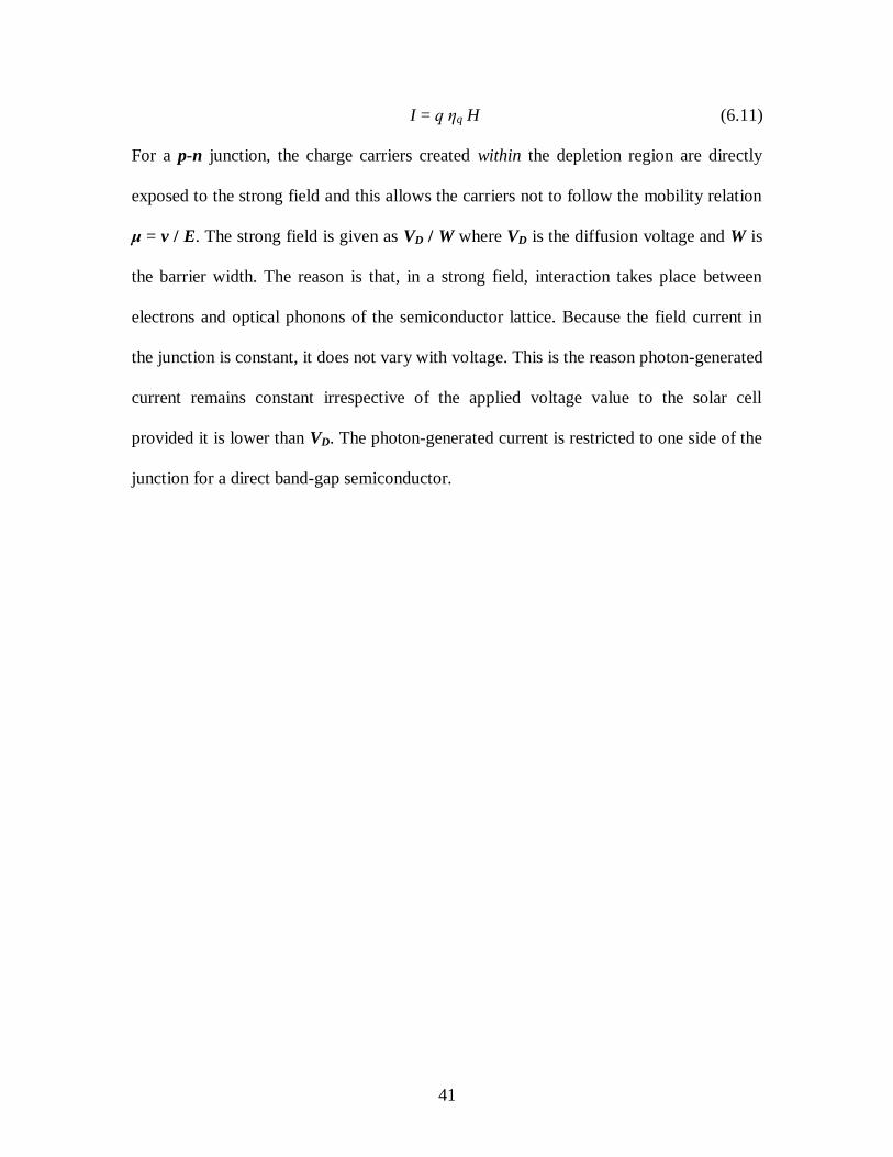
where a is obtained from semiconductor properties using a = q / kT and Eg is the
effective thermal energy gap. From equation (7.1), it is seen that maximum theoretical
efficiency of a solar cell is related with the semiconductor material energy gap. It is also a
function of spectral distribution of incident light and the temperature. If a p-n junction
has both the conduction band in the p-layer and the n-layer coinciding with the Fermi
level, then energy gap is equivalent to the maximum open-circuit voltage. This means an
increase in the band gap will see to a higher open-circuit voltage but will lead to a drop in
the short-circuit current and vice versa. This is because in materials with low band gaps,
their photon absorption edge is located at longer wavelengths and this shortcoming has to
be taken into account. The optimum band gap for solar cell of peak efficiency is between
1.4 and 1.6 eV. Figure 7.1 shows the maximum theoretical efficiency of semiconductors
as a function of their gap at room temperature.
Figure 7.1. Maximum theoretical conversion efficiency at room temperature for semiconductors, as a
function of band gaps [4]
Page 43
43
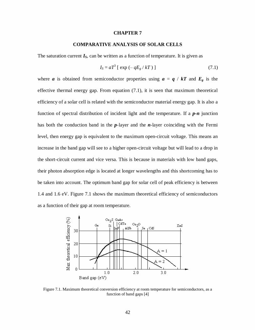
A is used as a result of the recombination current in the junction. The only snag with the
diagram above is that certain problems are not accounted for which do not allow for
maximum efficiency. The next diagram below (Figure 7.2) shows the variation of the
maximum theoretical efficiency calculated using equation (7.1) for different
temperatures. But the efficiency losses are also ignored. For a uniformly high steady-state
temperature, high concentration devices can be used with them. The decrease in
temperature, which is as a result of the Fermi level in the middle of the band gap leads to
a sharp efficiency decrease.
Figure 7.2. Temperature dependence of maximum efficiency [4]
For silicon solar cell under monochromatic visible light, the theoretical maximum
efficiency is about 45 – 50%. For AM-0, it is about 19%. On ground about 23 %.
Analysing the total system including the material used, its thickness and fabrication
techniques can lead to the reduction in the costs of solar cells by employing thin-film or
light absorbing technology and so on.
Page 44
44
REFERENCES
1. Bar-Lev A., (1997) Semiconductors and Electronic Devices, Prentice-Hall
International, London, 149-152.
2. Garg H. P., (1987) Heating, Agricultural and Photovoltaic Applications of Solar
Energy, Advances in Solar Energy Technology, Vol. 3, D. Reidel Publishing
Company, Holland, 279-285, 285-315, 325-329.
3. McMullan J. T. et al, (1979) Energy Resources and Supply, John Wiley and Sons,
New Jersey, 336-340.
4. Palz W., (1978) Solar Electricity: An Economic Approach To Solar Energy,
Butterworths and UNESCO, France, 179-189, 192, 217-223, 252-275.
5. Russell C. R., (1967) Elements Of Energy Conversion, 1st ed., Pergamon Press, New
York, 245-254.