DPMC, University of Geneva, CH-1211, Geneva 4, Switzerland
K. M. Rabe†
Department of Physics and Astronomy, Rutgers University, Piscataway, New Jersey 00854-8019, USA
J. F. Scott‡
Department of Earth Sciences, University of Cambridge, Cambridge CB2 3EQ, UnitedKingdom
�Published 17 October 2005�
This review covers important advances in recent years in the physics of thin-film ferroelectric oxides,the strongest emphasis being on those aspects particular to ferroelectrics in thin-film form. Theauthors introduce the current state of development in the application of ferroelectric thin films forelectronic devices and discuss the physics relevant for the performance and failure of these devices.Following this the review covers the enormous progress that has been made in the first-principlescomputational approach to understanding ferroelectrics. The authors then discuss in detail theimportant role that strain plays in determining the properties of epitaxial thin ferroelectric films.Finally, this review ends with a look at the emerging possibilities for nanoscale ferroelectrics, withparticular emphasis on ferroelectrics in nonconventional nanoscale geometries.
CONTENTS
I. Introduction 1084II. Ferroelectric Electronic Devices 1084
A. Ferroelectric memories 1084B. Future prospects for nonvolatile ferroelectric
memories 1086C. Ferroelectric field-effect transistors 1087D. Replacement of gate oxides in DRAMs 1088
III. Ferroelectric Thin-Film-Device Physics 1089A. Switching 1089
1. Ishibashi-Orihara model 10892. Nucleation models 10893. The scaling of coercive field with thickness 10904. Mobility of 90° domain walls 10905. Imaging of domain-wall motion 1090
B. Electrical characterization 10921. Standard measurement techniques 1092
a. Hysteresis 1092b. Current measurements 1093c. Dielectric permittivity 1093
2. Interpretation of dielectric permittivity data 1093a. Depletion charge versus intrinsic response 1093b. Domain-wall contributions 1094c. Dielectric measurements of phase transitions 1094
The aim of this review is to provide an account of theprogress made in the understanding of the physics offerroelectric thin-film oxides, particularly the physics rel-evant to present and future technology that exploits thecharacteristic properties of ferroelectrics. An overviewof the current state of ferroelectric devices is followedby identification and discussion of the key physics issuesthat determine device performance. Since technologi-cally relevant films for ferroelectric memories are typi-cally thicker than 120 nm, characterization and analysisof these properties can initially be carried out at compa-rable length scales. However, for a deeper understand-ing, as well as for the investigation of the behavior ofultrathin films with thickness on the order of lattice con-stants, it is appropriate to redevelop the analysis at thelevel of atomic and electronic structure. Thus, the sec-ond half of this review is devoted to a description of thestate of the art in first-principles theoretical investiga-tions of ferroelectric-oxide thin films, concluding with adiscussion of experiment and theory of nanoscale ferro-electric systems.
As a starting point for the discussion, it is helpful tohave a clear definition of ferroelectricity appropriate tothin films and nanoscale systems. Here we consider aferroelectric to be a pyroelectric material with two ormore stable states of different nonzero polarization. Un-like electrets, ferroelectrics have polarization states thatare thermodynamically stable, not metastable. Further-more, it must be possible to switch between the twostates by the application of a sufficiently strong electricfield, the threshold field being designated the coercivefield. This field must be less than the breakdown field ofthe material, or the material is merely pyroelectric andnot ferroelectric. Because of this switchability of thespontaneous polarization, the relationship between theelectric displacement D and the electric field E is hyster-etic.
For thin-film ferroelectrics the high fields that must beapplied to switch the polarization state can be achievedwith low voltages, making them suitable for integratedelectronics applications. The ability to create high-density arrays of capacitors based on thin ferroelectricfilms has spawned an industry dedicated to the commer-cialization of ferroelectric computer memories. The clas-sic textbooks on ferroelectricity �Fatuzzo and Merz,1967; Lines and Glass, 1967� though good, are now over20 years old, and predate the shift in emphasis from bulkceramics and single crystals towards thin-film ferroelec-trics. While much of the physics required to understandthin-film ferroelectrics can be developed from the under-standing of bulk ferroelectrics, there is also behaviorspecific to thin films that cannot be readily understood inthis way. This is the focus of the present review.
One of the points that will become clear is that aferroelectric thin film cannot be considered in isolation,but rather the measured properties reflect the entire sys-tem of films, interfaces, electrodes, and substrates. Wealso look in detail at the effects of strain on ferroelec-
trics. All ferroelectrics are grown on substrates whichcan impose considerable strains, meaning that propertiesof ferroelectric thin films can often be considerably dif-ferent from those of their bulk parent material. Theelectronic properties also have a characteristic behaviorin thin-film form. While bulk ferroelectric materials aretraditionally treated as good insulators, as films becomethinner it becomes more appropriate to treat them assemiconductors with a fairly large band gap. These ob-servations are key to understanding the potential andthe performance of ferroelectric devices, and to under-standing why they fail when they do.
In parallel with the technological developments in thefield, the power of computational electronic structuretheory has increased dramatically, giving us new ways ofunderstanding ferroelectricity. Over the last 15 years,more and more complex systems have been simulatedwith more accuracy; and as the length scales of experi-mental systems decrease, there is now an overlap in sizebetween the thinnest epitaxial films and the simulatedsystems. It is therefore an appropriate and exciting timeto review this work, and to make connections between itand the problems considered by experimentalists andengineers.
Finally, we look at some issues and ideas in nanoscaleferroelectrics, with particular emphasis on new geom-etries for ferroelectric materials on the nanoscale suchas ferroelectric nanotubes and self-patterned arrays offerroelectric nanocrystals.
We do not attempt to cover some of the issues whichare of great importance but instead refer readers to re-views by other authors. Some of the more importantapplications for ferroelectrics make use of their piezo-electric properties, for example, in actuators and mi-crosensors; this topic has been reviewed by Muralt�2000�. Relaxor ferroelectrics in which ferroelectric or-dering occurs through the interaction of polar nano-domains induced by substitution are also of great inter-est for a number of applications and have recently beenreviewed by Samara �2003�.
II. FERROELECTRIC ELECTRONIC DEVICES
A. Ferroelectric memories
The idea that electronic information can be stored inthe electrical polarization state of a ferroelectric mate-rial is a fairly obvious one; however, its realization is notso straightforward. The initial barrier to the develop-ment of ferroelectric memories was the necessity ofmaking them extremely thin films because the coercivevoltage of ferroelectric materials is typically of the orderof several kV/cm, requiring submicron thick films tomake devices that work on the voltage scale required forcomputing �all Si devices work at �5 V�. With today’sdeposition techniques this is no longer a problem, andnow high-density arrays of nonvolatile ferroelectricmemories are commercially available. However, reliabil-ity remains a key issue. The lack of good device modelsmeans that the design of ferroelectric memories is ex-
1084 Dawber, Rabe, and Scott: Physics of thin-film ferroelectric oxides
Rev. Mod. Phys., Vol. 77, No. 4, October 2005
pensive and that it is difficult to be able to guaranteethat a device will still operate ten years into the future.Because competing nonvolatile memory technologiesexist, ferroelectric memories can succeed only if theseissues are resolved.
A ferroelectric capacitor, while capable of storing in-formation, is not sufficient for making a nonvolatilecomputer memory. A pass-gate transistor is required sothat a voltage above the coercive voltage is only appliedto the capacitor when a voltage is applied to both theword and bit line; this is how one cell is selected from anarray of memories. The current measured through asmall load resistor in series with the capacitor is com-pared to that from a reference cell that is poled in adefinite direction. If the capacitor being read is in a dif-ferent state, the difference in current will be quite largewhere the displacement current associated with switch-ing accounts for the difference. If the capacitor does notswitch because it is already in the reference state, thedifference in current between the capacitor being readand the reference capacitor is zero.
Most memories use either a 1 transistor–1 capacitor�1T-1C� design or a 2 transistor–2 capacitor �2T-2C� de-sign �Fig. 1�. The important difference is that the 1T-1Cdesign uses a single reference cell for the entire memoryfor measuring the state of each bit, whereas in the 2T-2Cthere is a reference cell per bit. A 1T-1C design is muchmore space effective than a 2T-2C design, but has somesignificant problems, most significantly that the refer-ence capacitor will fatigue much faster than the othercapacitors, and so failure of the device occurs morequickly. In the 2T-2C design the reference capacitor ineach cell fatigues at the same rate as its correspondingstorage capacitor, leading to better device life. A prob-lem with these designs is that the read operation is de-structive, so every time a bit is read it needs to be writ-ten again. A ferroelectric field-effect transistor, in whicha ferroelectric is used in place of the metal gate on afield-effect transistor, would both decrease the size ofthe memory cell and provide a nondestructive readout;however, no commercial product has yet been devel-oped. Current efforts seem to run into serious problemswith data retention.
An example of a real commercially available memoryis the Samsung lead zirconate titanate-based 4 Mbit1T-1C ferroelectric memory �Jung et al., 2004�. The scan-ning electron microscopy cross section �Fig. 2� of thedevice gives some indication of the complexity of designinvolved in a real ferroelectric memory.
Lead zirconate titanate �PZT� has long been the lead-ing material considered for ferroelectric memories,though strontium bismuth tantalate �SBT�, a layeredperovskite, is also a popular choice due to its superiorfatigue resistance and the fact that it is lead-free �Fig. 3�.However, it requires higher-temperature processing,which creates significant integration problems. Recentlyprogress has been made in optimizing precursors. Untilrecently the precursors for Sr, Bi, and Ta/Nb did notfunction optimally in the same temperature range, butlast year Inorgtech developed Bi�mmp�3—a 2-methoxy-2-propanol propoxide that improves reaction and lowersthe processing temperature for SBT, its traditional maindisadvantage compared to PZT. This material also satu-rates the bismuth coordination number at 6. Recentlyseveral other layered perovskites, for example, bismuthtitanate, have also been considered.
FIG. 1. �a� 1T-1C memory design. When a voltage is applied to both the word and bit line, the memory cell is addressed. Alsoshown is the voltage applied to the capacitor and the current output, depending on whether a one or a zero is stored. The currentfor the zero state is pure leakage current and by comparison to a reference capacitor can be removed. �b� A 2T-2C memory cellin which the reference capacitor is part of the memory cell.
FIG. 2. Cross-sectional SEM image of the Samsung 4 Mbit1T-1C 3 metal FRAM.
1085Dawber, Rabe, and Scott: Physics of thin-film ferroelectric oxides
Rev. Mod. Phys., Vol. 77, No. 4, October 2005
As well as their applications as ferroelectric randomaccess memories �FRAMs�, ferroelectric materials havepotential use in dynamic random access memories�DRAMs� because of their high dielectric constant inthe vicinity of the ferroelectric phase transition, a topicwhich has been reviewed by Kingon, Maria, and Streif-fer �2000�. Barium strontium titanate �BST� is one of theleading materials in this respect since by varying thecomposition a transition temperature just below roomtemperature can be achieved, leading to a high dielectricconstant over the operating temperature range.
B. Future prospects for nonvolatile ferroelectric memories
There are two basic kinds of ferroelectric random ac-cess memories in production today: �1� the free-standingRAMs and �2� fully embedded devices �usually a CPU,which may be a complementary metal-oxide semicon-ductor electrically erasable programmable read-onlymemory �CMOS EEPROM�, the current generationwidely used nonvolatile memory technology, plus aFRAM and an 8-bit microprocessor�. The former havereached 4 Mbit at both Samsung �using PZT� and Mat-sushita �using SBT�. The Samsung device is not yet, asfar as the authors know, in commercial production forreal products, but the NEC FRAM is going into full-scale production this year in Toyama �near Kanazawa�.Fujitsu clearly leads in the actual commercial use of itsembedded FRAMs. The Fujitsu-embedded FRAM isthat used in the SONY Playstation 2. It consists of 64Mbit of EEPROM plus 8 kbit of RAM, 128-kbit ROM,and a 32-kbit FRAM plus security circuit. The device ismanufactured with a 0.5-�m CMOS process. The ca-pacitor is 1.6�1.9 �m2 and the cell size is either27.3 �m2 for the 2T-2C design or 12.5 �m2 for the 1T-1C.
The leading competing technologies in the long termfor nonvolatile computer memories are FRAM andmagnetic random access memories �MRAM�. These aresupposed to replace EEPROMs �electrically erasableprogramable read-only memories� and “Flash” memo-ries in devices such as digital cameras. Flash, thoughproving highly commercially successful at the moment,is not a long-term technology, suffering from poor long-term endurance and scalability. It will be difficult for
Flash to operate as the silicon logic levels decrease from5 at present to 3.3, 1.1, and 0.5 V in the near future. Themain problem for ferroelectrics is the destructive readoperation, which means that each read operation mustbe accompanied by a write operation leading to fasterdegradation of the device. The operation principle ofMRAMs is that the tunneling current through a thinlayer sandwiched between two ferromagnetic layers isdifferent depending on whether the ferromagnetic layershave their magnetization parallel or antiparallel to eachother. The information stored in MRAMs can thus beread nondestructively, but their write operation requireshigh power which could be extremely undesirable inhigh-density applications. We present a summary of thecurrent state of development in terms of design rule andspeed of the two technologies in Table I.
Partly in recognition of the fact that there are distinctadvantages for both ferroelectrics and ferromagnets,there has been a recent flurry of activity in the field ofmultiferroics, i.e., materials that display both ferroelec-tric and magnetic ordering, the hope being that onecould develop a material with a strong enough couplingbetween the two kinds of ordering to create a devicethat can be written electrically and read magnetically. Ingeneral multiferroic materials are somewhat rare, andcertainly the conventional ferroelectrics such as PbTiO3
and BaTiO3 will not display any magnetic behavior asthe Ti-O hybridization required to stabilize the ferro-electricity in these compounds will be inhibited by thepartially filled d orbitals that would be required for mag-netism �Hill, 2000�. However, there are other mecha-nisms for ferroelectricity and in materials where ferro-electricity and magnetism coexist there can be couplingbetween the two. For example, in BaMnF4 the ferroelec-tricity is actually responsible for changing the antiferro-magnetic ordering to a weak canted ferromagnetism�Fox et al., 1980�. In addition, the large magnetoelectriccoupling in these materials causes large dielectricanomalies at the Néel temperature and at the in-planespin-ordering temperature �Scott, 1977, 1979�. More re-cent theoretical and experimental efforts have focusedon BiMnO3, BiFeO3 �Seshadri and Hill, 2001; Moreirade Santos et al., 2002; Wang et al., 2003� and YMnO3�Fiebig et al., 2002; Van Aken et al., 2004�.
1086 Dawber, Rabe, and Scott: Physics of thin-film ferroelectric oxides
Rev. Mod. Phys., Vol. 77, No. 4, October 2005
C. Ferroelectric field-effect transistors
It has been known for some time that replacing themetal gate in a field-effect transistor �FET� by a ferro-electric could produce a device with nondestructivereadout in which the polarization of the gate �+ for “1”and − for “0”� could be sensed simply by monitoring thesource-drain current magnitude. Thus such a device re-quires no reset operation after each READ and will ex-perience very little fatigue in a normal frequent-read,occasional-write usage. The first mention of the idea of aferroelectric FET is in the U.S. patent of Ross �1957�and the first realization was by Moll and Tarui �1963�,while the first attempt to fabricate one on silicon was byWu �1974�. The early ferroelectric FETs utilized gates oflithium niobate �Rice University; Rabson et al., 1995� orBaMgF4 �Westinghouse; Sinharoy et al., 1991, 1992,1993�. An example of a ferroelectric FET device as fab-ricated by Mathews et al. �1997� is shown in Fig. 4.
The optimum parameters for such a ferroelectric-gatematerial are extremely different from those for pass-gate-switched capacitor arrays; in particular, the latterrequire a remanent polarization �10 �C/cm2, whereasthe ferroelectric-gated FETs can function well with 50times less �0.2 �C/cm2�. However, the switched capaci-tor array �FRAM� is very tolerant of surface traps in theferroelectric �which may be �1020 cm−3 in the interface
region near the electrode� since the ferroelectric makescontact only with a metal �or metal-oxide� electrode. Bycomparison, the ferroelectric gate in an FET contactsthe Si substrate directly �metal-oxide-semiconductorfield-effect-transistor channel�. Thus it must be bufferedfrom the Si to prevent charge injection. Unfortunately, ifa thin buffer layer of a low-dielectric material such asSiO2 is used, most of the applied voltage will drop acrossthe buffer layer and not the ferroelectric gate, making itimpossible to switch the gate. As a result, much of theferroelectric FET research has employed buffer layerswith relatively high dielectric constants, or else ratherthick buffer layers, for example, the first BaMnF4 FETmade at Symetrix �Scott, 1998� used a buffer layer of�40 nm of SiO2. Subsequent studies often used PZT�Kalkur et al., 1994� although the large remanent polar-ization in this case ��40 �C/cm2� is actually undesirablefor a ferroelectric FET gate.
As pointed out by Yoon and Ishiwara �2001�, the de-polarization field in a ferroelectric gate is inevitably gen-erated when the gate is grounded, and this makes it verydifficult to obtain �10 year data retention in an FE-FET.Their solution is to utilize a 1T-2C capacitor geometry inwhich this depolarization field is suppressed by polingthe two capacitors in opposite directions. With thisscheme Ishiwara and his colleagues achieved an on/offsource-drain current ratio of �1000 for a 150-nm-thickSBT film in a 5�50 �m2 metal-oxide-semiconductorfield-effect transistor channel, with Pt electrodes on theSBT capacitor.
Note that the direct contact of the ferroelectric ontoSi produces a semiconductor junction that is quite differ-ent from the metal-dielectric interface discussed above.The Schottky barrier heights for this case have been cal-culated by Peacock and Robertson �2002�. The electronscreening length in the Si will be much greater than inthe case of metal electrodes; in particular, this will in-crease the minimum ferroelectric film thickness requiredto stabilize the device against depolarization instabili-ties. Although this point was first emphasized by Batra
TABLE I. Some clarification of the numbers presented here isrequired. The size of the Fujitsu FRAM memory may seemsmall but it is for an actual commercial device in large-scaleuse �in every Playstation 2�, whereas the others are figuresfrom internal sampling of unreleased devices that have notbeen commercialized. No MRAMs exist in any commercialdevice, giving FRAMs a substantial edge in this regard. Themost recent commercial FRAM product actually shipped is alarge-cell-area six-transistor four-capacitor �6T-4C� memoryfor smart credit cards and radio-frequency identification tags�RF-ID� and features nondestructive readout �Masui et al.,2003�. A total of 2�108 ferroelectric memories of all typeshave been sold industry wide. The Sony MRAM, though small,has submicron design rules, meaning that in principle a work-ing device could be scaled up to Mb size.
CompanyDesign rule
�feature size�Speed
�access time�
MRAMsNEC/Toshiba 1 Mb
IBM 16 MbMatsushita 4 Mb
Sony 8kb 0.18 �mCypress 256 kb 70 ns
State of the art 16 Mb 0.09 �m 25 nsFRAMsFujitsu 32 kb 100 ns
1087Dawber, Rabe, and Scott: Physics of thin-film ferroelectric oxides
Rev. Mod. Phys., Vol. 77, No. 4, October 2005
and Silverman �1972�, it has been neglected in the morerecent context of ferroelectric FETs. In our opinion, thisdepolarization instability for thin ferroelectric gates onFETs is a significant source of the observed retentionfailure in the devices but has not yet been explicitlymodeled. If we are correct, the retention problem inferroelectric FETs could be minimized by making theferroelectric gates thicker and the Si contacts more con-ducting �e.g., p+ rather than p�. See Scott �2005� for afull discussion of all-perovskite FETs.
Table II lists a number of the most promising gatematerials under recent study, together with the bufferlayers employed in each case. Studies of the I�V� char-acteristics of such ferroelectric FETs have been given byMacleod and Ho �2001� and a disturb-free programmingscheme described by Ullman et al. �2001�.
Beyond its use in modulating the current in a semi-conductor channel the ferroelectric field effect can alsobe used to modify the properties of more exotic corre-lated oxide systems �Ahn, Triscone, and Mannhart,2003�.
D. Replacement of gate oxides in DRAMs
At present there are three basic approaches to solvingthe problem of SiO2-gate oxide replacement forDRAMs. The first is to use a high-dielectric �“high-k”�material such as SrTiO3 �k=300 is the dielectric con-stant; �=k−1 is the permittivity; for k�1 the terms are
nearly interchangeable� deposited by some form of epi-taxial growth. This is the technique employed at Mo-torola, but the view elsewhere is that it is too expensiveto become industry process worthy. The second ap-proach is to use a material of moderate k �of order 20�,with HfO2 favored but ZrO2 also a choice. Hafnium ox-ide is satisfactory in most respects but has the surprisingdisadvantage that it often degrades the n-channel mobil-ity catastrophically �by as much as 10 000 times�. Re-cently ST Microelectronics decided to use SrTiO3 butwith metal-organic chemical-vapor deposition from Aix-tron, thus combining high dielectric constant andcheaper processing.
The specific high-k integration problems are the fol-lowing four: �1� depletion effects in the polysilicon gate,�2� interface states, �3� strain effects, and �4� etching dif-ficulties �HfO2 is hard to wet etch�. The use of a poly-Sigate instead of a metal gate produces grain-boundarystress in the poly, with resultant poor conductivity. Thismobility degradation is only partly understood. The gen-eral view is that a stable amorphous HfO2 would be agood strain-free solution. Note that HfO2 normally crys-tallizes into two or three phases, one of which is mono-clinic �Morrison et al., 2003�. Hurley in Cork has beenexperimenting with a liquid injection system that re-sembles Isobe’s earlier SONY device for deposition ofviscous precursors with flash evaporation at the target.
TABLE II. A number of the most promising gate materials under recent study, together with thebuffer layers employed in each case. Studies of the I�V� characteristics of such ferroelectric FETshave been given by Macleod and Ho �2001� and a disturb-free programming scheme described byUllman et al. �2001�.
FET gate Buffer layer Reference
LiNbO3 none Rabson et al. �1995�SBT SrTa2O6 Ishiwara �1993�,
Ishiwara et al. �1997�,Ishiwara �2001�
SBT CeO2 Shimada et al. �2001�,Haneder et al. �2001�
SBT SiO2 Okuyuma et al. �2001�SBT ZrO2 Park and Oh �2001�SBT Al2O3 Shin et al. �2001�SBT Si3N4 Han et al. �2001�SBT Si3N4/SiO2 Sugiyama et al. �2001�SBT poly-Si+Y2O3 Kalkur and Lindsey �2001�
Pb5Ge3O11 none Li and Hsu �2001�YMnO3 Y2O3 Cheon et al. �2001�,
Choi et al. �2001�Sr2�Ta2xNb2−2x�O7 none Kato �2001�
PZT CeO2 Xiaohua et al. �2001�BST�strained� YSZ�zirconia� Jun and Lee �2001�
BaMnF4 SiO2 Scott �1998�,Kalkur et al. �1994�
1088 Dawber, Rabe, and Scott: Physics of thin-film ferroelectric oxides
Rev. Mod. Phys., Vol. 77, No. 4, October 2005
III. FERROELECTRIC THIN-FILM-DEVICE PHYSICS
We now turn to some of the physics questions whichare relevant to ferroelectric thin-film capacitors.
A. Switching
In the ferroelectric phase, ferroelectric materials formdomains where the polarization is aligned in the samedirection in an effort to minimize energy. When a field isapplied, the ferroelectric switches by the nucleation ofdomains and the movement of domain walls and not bythe spontaneous reorientation of all of the polarizationin a domain at once. In contrast to ferromagnets, whereswitching usually occurs by the sideways movement ofexisting domain walls, ferroelectrics typically switch bythe generation of many new reverse domains at particu-lar nucleation sites, which are not random; i.e., nucle-ation is inhomogeneous. The initial stage is nucleation ofopposite domains at the electrode, followed by fast for-ward propagation of domains across the film, and thenslower widening of the domains �Fig. 5�. In perovskiteoxides the final stage of the switching is usually muchslower than the other two stages, as first established byMerz �1954�. In other materials nucleation can be theslowest �rate-limiting� step.
1. Ishibashi-Orihara model
For many years the standard model to describe thisprocess has been the Ishibashi-Orihara model �Oriharaet al., 1994� based on Kolomogorov-Avrami growth ki-netics. In this model one considers a nucleus formed attime t� and then a domain propagating outwards from itwith velocity V. In the Ishibashi-Orihara model the ve-locity is assumed to be dependent only on the electricfield E, and not on the domain radius r�t�. This makesthe problem analytically tractable but gives rise to un-physical fitting parameters, such as fractional dimension-ality D. The fractional D is not related to fractals. It isan artifact that arises because the domain-wall velocityV is actually proportional to 1/r�t� for each domain andis not a constant at constant E. The volume of a domainat time t is given by
C�t,t�� = CD��t�
t
V�t��dt��D
, �1�
where D is the dimensionality of the growth and CD is aconstant which depends on the dimensionality. It is alsoassumed within this model that the nucleation is deter-ministic and occurs at predefined places; i.e., this is amodel of inhomogeneous nucleation. This is an impor-tant point since some researchers still use homogeneousnucleation models. These are completely inappropriatefor ferroelectrics �where the nucleation is inhomoge-neous, as is demonstrated by imaging experiments �Shur,1996; Shur et al., 2000; Ganpule et al., 2001��.
The result of the model is that the fraction of switchedcharge as a function of field and frequency may be ex-pressed as
Q�E,f� = 1 − exp�− f−D��E�� , �2�
where ��E� depends on the wave form used for switch-ing. After some consideration and the substitution��E�=Ek one obtains a useful relationship for the de-pendence of the field on frequency:
Ec = fD/k. �3�
This relationship has been used to fit data fairly wellin TGS �Hashimoto et al., 1994�, PZT, and SBT �Scott,1996�. More recently, however, Tsurumi et al. �2001� andJung et al. �2002� have found that over larger frequencyranges the data on several materials is better fitted bythe nucleation-limited model of Du and Chen �1998a�.Tagantsev et al. �2002� have also found that over largetime ranges the Ishibashi-Orihara model is not a gooddescription of switching-current data and that anucleation-limited model is more appropriate. It is quitepossible of course that domain-wall-limited switching�Ishibashi� is operative in one regime of time and fieldbut that in another regime the switching is nucleationlimited.
2. Nucleation models
Some of the earliest detailed studies of switching inferroelectrics developed nucleation-limited switchingmodels where the shape of the nucleus of the reverseddomain was very important. In the work of Merz �1954�and Wieder �1956, 1957� a nucleation-limited model wasused in which when dagger-shaped nuclei were assumed,the correct dependence of the switching current on elec-tric field could be derived. This approach leads to theconcept of an activation field for nucleation �somewhatdifferent from the coercive field�. Activation fields inthin-film PZT capacitors were measured by Scott et al.�1988�; very recently, Jung et al. �2004� have studied theeffects of microgeometry on the activation field in PZTcapacitors.
The switching model of Tagantsev et al. �2002� is adifferent approach in which a number of noninteractingelementary switching regions are considered. Theseswitch according to a broad distribution of waiting times.
FIG. 5. The three phases of domain reversal: I, nucleation�fast�; II, forward growth �fast�; III, sideways growth �slow�.
1089Dawber, Rabe, and Scott: Physics of thin-film ferroelectric oxides
Rev. Mod. Phys., Vol. 77, No. 4, October 2005
3. The scaling of coercive field with thickness
For the last 40 years the semiempirical scaling law�Janovec, 1958; Kay and Dunn, 1962�, Ec�d��d−2/3, hasbeen used successfully to describe the thickness depen-dence of the coercive field in ferroelectric films rangingfrom 100 �m to 200 nm �Scott, 2000b�. In the ultrathinPVDF films of Bune et al. �1998� a deviation from thisrelationship was seen for the thinnest films �Ducharmeet al., 2000�. Although they attribute this to a new kindof switching taking place �simultaneous reversal of po-larization, as opposed to nucleation and growth of do-mains�, Dawber, Chandra, et al. �2003� have shown, tothe contrary, that if the effects of a finite depolarizationfield due to incomplete screening in the electrode aretaken into account, then the scaling law holds over sixdecades of thickness and the coercive field does not de-viate from the value predicted by the scaling law �Fig. 6�.Recently, Pertsev et al. �2003� measured coercive fieldsin very thin PZT films. Although they have used a dif-ferent model to explain their data, it can be seen that infact the scaling law describes the data very well.
4. Mobility of 90° domain walls
The mobility of domain walls, especially 90° walls, de-pends upon their width. In this respect the question hasbeen controversial, with some authors claiming very
wide widths �hundreds of angstroms� and immobilewalls. Some recent papers show experimentally that 90°domain walls in perovskite ferroelectrics are extremelynarrow �Tsai et al., 1992; Stemmer et al., 1995; Floquet etal., 1997; Foeth et al., 1999�. In PbTiO3 they are1.0±0.3 nm wide. This connects the general question ofhow wide they are and whether they are immobile. Thereview by Floquet and Valot �1999� is quite good. Theymake the point that in ceramics these 90° walls are 14.0nm wide �an order of magnitude wider than in singlecrystals�. This could be why theory and experiment dis-agree, i.e., that something special in the ceramics makesthem 10–15 times wider �and less mobile?�. The latterpoint is demonstrated clearly in experiments on KNbO3,together with a theoretical model that explains geo-metrical pinning in polyaxial ferroelectrics in terms ofelectrostatic forces. In this respect the first-principlesstudy of Meyer and Vanderbilt �2002� is extremely inter-esting. Not only do they show that 90° domain walls inPbTiO3 are narrow and form much more easily than180° domain walls, but that they should be much moremobile as well, the barrier for motion being so low theypredict thermal fluctuation of about 12 unit cells at roomtemperature, which could perhaps explain why they ap-pear to be wide.
Some experimental studies using atomic force micros-copy have attempted to answer the question of whether90° domain walls were mobile or not. In certain circum-stances they were immobile �Ganpule, Nagarajan, Li, etal., 2000; Ganpule, Nagarajan, Ogale, et al., 2000�, but inanother study �Nagarajan et al., 2003� the motion of 90°domain walls under an applied field was directly ob-served. It seems that in principle 90° domain walls canmove, but this depends quite strongly on the sampleconditions. Recently Shilo et al. �2004� and Salje and Lee�2004� have shown that domain wall widths are not acharacteristic of the material per se but vary greatly withlocation in the sample due to nearby impurities. Thisreconciles the diverse values reported.
5. Imaging of domain-wall motion
The direct imaging of ferroelectric domain walls is anexcellent method for understanding domain-wall motionand switching. At first this was carried out in materialswhere the domains were optically distinct such as leadgermanate �Shur et al., 1990�, but more recently atomicforce microscopy has become a powerful tool for ob-serving domain-wall motion. The polarization at a pointcan be obtained from the piezoresponse detected by thetip, and the tip itself can be used to apply a field to theferroelectric sample and initiate switching. It is thus pos-sible to begin switching events and watch their evolutionover time. Atomic force microscopy domain writing offerroelectric domains can also be used to write ex-tremely small domain structures in high-density arrays�Paruch et al., 2001� or other devicelike structures, suchas surface acoustic wave devices �Sarin Kumar et al.,2004�.
FIG. 6. �Color� The scaling of coercive field with thickness inferroelectrics; from mm to nm scale. From Dawber, Chandra,et al., 2003. The bottom is the three sets of data from the upperall normalized to the same value at 10−6.5 m.
1090 Dawber, Rabe, and Scott: Physics of thin-film ferroelectric oxides
Rev. Mod. Phys., Vol. 77, No. 4, October 2005
The backswitching studies of Ganpule et al. �2001�show two very interesting effects �Fig. 7�. The first is thefinding that reverse domains nucleate preferentially atantiphase boundaries. This was studied in more detailsubsequently by Roelofs et al. �2002� who invoked adepolarization-field-mediated mechanism to explain theresult. Another explanation might be that the strain isrelaxed at these antiphase boundaries resulting in favor-able conditions for nucleation. Second, the influence ofcurvature on the domain-wall relaxation is accounted forwithin the Kolomogorov-Avrami framework. The veloc-ity of the domains is dependent on curvature, and, as therelaxation proceeds, the velocity decreases and the do-main walls become increasingly faceted. In Fig. 7 thewhite polarization state is stable, whereas the black isnot. The sample is poled into the black polarization stateand then allowed to relax back.
A different kind of study was undertaken by Tybell etal. �2002�, in which they applied a voltage pulse to switcha region of the ferroelectric using an atomic force mi-croscopy tip and watched how the reversed domain grewas a function of pulse width and amplitude. They wereable to show that the process was well described by acreep mechanism thought to arise due to random pin-ning of domain walls in a disordered system �Fig. 8�.Though the exact origin of the disorder was not clear, itsuggests that it is connected to oxygen vacancies, whichalso play a role in pinning the domain walls during a
fatigue process due to their ordering �Park and Chadi,1998; Scott and Dawber, 2000�.
An unsolved puzzle is the direct observation viaatomic force microscopy of domain walls penetratinggrain boundaries �Gruverman et al., 1997�. This is con-trary to some expectations and always occurs at non-normal incidence, i.e., at a small angle to the grainboundary.
One of the interesting things to come out of the workin lead germanate �where ferroelectric domains are op-tically distinct due to electrogyration� by Shur et al.�1990� is that at high applied electric fields �15 kV cm−1�tiny domains are nucleated in front of the moving do-main wall �Fig. 9�. A very similar effect is seen in ferro-magnets as observed by Randoshkin �1995� in a single-crystal iron-garnet film.
However, in ferromagnets the effect is modeled by aspin-wave mechanism �Khodenkov, 1975�. This mecha-nism is based on the gyrotropic model of domain-wallmotion in uniaxial materials �Walker, 1963�. When astrong magnetic driving field �exceeding the Walkerthreshold� acts upon a domain wall, the magnetizationvectors in the domain wall begin to precess with a fre-quency H, where is the effective gyromagnetic ratio.By relating the precession frequency in the domain wallwith the spin-wave frequency in the domain, good pre-dictions can be made for the threshold fields at whichthe effect occurs. We note that the domains nucleated in
FIG. 7. Piezoresponse scans of a single cell inPbZr0.2Ti0.8O3. �b�–�d� The spontaneous re-versal of polarization within this region afterwait times of �b� 1.01�103, �c� 1.08�105, �d�1.61�105, and �e� 2.55�105 s. Faceting canbe seen in �c�, �d�, and �e�. �f� Transformation-time curve for the data in �b�–�e�. From Gan-pule et al., 2001.
FIG. 8. �a� Domain size increases logarithmi-cally with pulse widths longer than 20 �s andsaturates for shorter times as indicated by theshaded area. �b� Domain-wall speed as a func-tion of the inverse applied electric field for290-, 370-, and 810-Å-thick samples. The datafit well the characteristic velocity-field rela-tionship of a creep process. From Tybell et al.,2002.
1091Dawber, Rabe, and Scott: Physics of thin-film ferroelectric oxides
Rev. Mod. Phys., Vol. 77, No. 4, October 2005
front of the wall may be considered as vortexlike Skyr-mions. The similarity between these effects is thus quitesurprising and suggests that perhaps there is more incommon between ferroelectric domain-wall motion andferromagnet domain-wall motion than is usually consid-ered. However, whereas Democritov and Kreines �1988�have shown that magnetic domain walls can be drivensupersonically �resulting in a phase-matched Cherenkov-like bow wave of acoustic phonon emission�, there is nodirect evidence of supersonic ferroelectric domains. Pro-cesses such as the nanodomain nucleation describedabove seem to occur instead when the phase velocity ofthe domain-wall motion approaches the speed of sound.Of course the macroscopic electrical response to switch-ing can arrive at a time tv /d, where v is the soundvelocity and d the film thickness, simply from domainnucleation within the interior of the film between cath-ode and anode.
B. Electrical characterization
1. Standard measurement techniques
Several kinds of electrical measurements are made onferroelectric capacitors. We briefly introduce them herebefore proceeding to the following sections where wediscuss in detail the experimental results obtained byusing these techniques.
a. Hysteresis
One of the key measurements is naturally the mea-surement of the ferroelectric hysteresis loop. There aretwo measurement schemes commonly used. Tradition-ally a capacitance bridge as first described by Sawyerand Tower �1930� was used �Fig. 10�. Although this is nolonger the standard way of measuring hysteresis, the cir-cuit is still useful �and very simple and cheap� and wehave made several units which are now in use in theteaching labs in Cambridge for a demonstration in whichstudents are able to make and test their own ferroelec-tric KNO3 capacitor �Dawber, Farnan, and Scott, 2003�.
This method is not very suitable in practice for manyreasons, for example, the need to compensate for dielec-tric loss and the fact that the film is being continuouslycycled. Most testing of ferroelectric capacitors is now
carried out using commercial apparatus from one of twocompanies, Radiant Technologies and AixAcct. Bothcompanies’ testers can carry out a number of tests andmeasurements, and both machines use charge or currentintegration techniques for measuring hysteresis. Bothmachines also offer automated measurement of charac-teristics such as fatigue and retention.
In measuring P�E� hysteresis loops several kinds ofartifacts can arise. Some of these are entirely instrumen-tal, and some arise from the effects of conductive �leaky�specimens.
Hysteresis circuits do not measure polarization P di-rectly. Rather, they measure switched charge Q. For anideal ferroelectric insulator
Q = 2PrA , �4�
where Pr is the remanent polarization and A is the elec-trode area for a parallel-plate capacitor. For a somewhatconductive sample
Q = 2PrA + �Eat , �5�
where � is the electrical conductivity, Ea is the appliedfield, and t the measuring time. Thus Q in a pulsed mea-suring system depends on the pulse width.
The four basic types of apparent hysteresis curves thatare artifacts are shown in Fig. 11.
FIG. 9. Nucleation of nanodomains in front of domain wall inlead germanate at high electric field. Black and white representthe two directions of polarization. From Gruverman, 1990.
FIG. 10. �a� The original Sawyer-Tower circuit, �b� hysteresisin Rochelle salt measured using this circuit by Sawyer andTower at various temperatures. From Sawyer and Tower, 1930.
FIG. 11. Common hysteresis artifacts: �a� dead short, �b� linearlossy dielectric, �c� saturated amplifier, and �d� nonlinear lossydielectric.
1092 Dawber, Rabe, and Scott: Physics of thin-film ferroelectric oxides
Rev. Mod. Phys., Vol. 77, No. 4, October 2005
Figure 11�a� is a dead short in a Sawyer-Tower circuitor modern variant and is discussed in the instructiondocumentation for both the AixAcct1 and Radiant2
testers.Figure 11�b� shows a linear lossy dielectric. The points
where the loop crosses Va=0 are often misinterpreted asPr values. Actually this curve is a kind of Lissajous fig-ure. It can be rotated out of the page to yield a straightline �linear dielectric response�. Such a rotation can bedone electrically and give a “compensated” curve. Herecompensation means to compensate the phase shiftcaused by dielectric loss.
Figure 11�c� is more subtle. Here are two seeminglyperfect square hysteresis loops obtained on the same ornominally equivalent specimens at different maximumfields. The smallest loop was run at an applied voltage ofVa=10 V, and yields Pr=30 �C cm−2 and the larger atVa=50 V and yields Pr=100 �C cm−2. Note that bothcurves are fully saturated �flat tops�. This is impossible.If the dipoles of the ferroelectric are saturated at Pr
=30 �C cm−2 then there are no additional dipoles toproduce Pr=100 �C cm−2 in the larger loop at high volt-age. What actually occurs in the illustration is saturationof the amplifier in the measuring system, not saturationof the polarization in the ferroelectric. The figure istaken from Jaffe, Cook, and Jaffe �1971� where this ef-fect is discussed �p. 39�. It will be a serious problem ifconductivity is large in Eq. �5�. “Large” in this sense is��10−6 �� cm�−1 and “small” is �10−7 �� cm�−1. Thisis probably the source of Pr�150 �C cm−2 reports inBiFeO3 where � can exceed 10−4 �� cm�−1.
Finally, Fig. 11 is a nonlinear lossy dielectric. If it isphase compensated it still resembles real hysteresis. Onecan verify whether it is real or an artifact only by varyingthe measuring frequency. Artifacts due to dielectric lossare apt to be highly frequency dependent. Figures 11�b�and 11�d� are discussed in Lines and Glass �1967, p. 104�.
No data resembling Figs. 11�a�–11�d� should be pub-lished as ferroelectric hysteresis.
b. Current measurements
Another measurement of importance which is carriedout in an automated way by these machines is the mea-surement of the leakage current. This is normally dis-cussed in terms of a current-voltage �I-V� curve, wherethe current is measured at a specified voltage. It is im-portant, however, that sufficient time is allowed for eachmeasurement step so that the current is in fact truesteady-state leakage current and not relaxation current.For this reason current-time �I-t� measurements can alsobe important �Dietz and Waser, 1995�. Relaxation timesin ferroelectric oxides such as barium titanate are typi-cally 1000 s at room temperature.
c. Dielectric permittivity
An impedance analyzer measures the real and imagi-nary parts of the impedance by use of a small-amplitudeac signal which is applied to the sample. The actual mea-surement is then made by balancing the impedance ofthe sample with a set of references inside the impedanceanalyzer. From this the capacitance and loss can be cal-culated �all this is done automatically by the machine�. Itis possible at the same time to apply a dc bias to thesample, so the signal is now a small ac ripple superim-posed on a dc voltage. Ferroelectric samples display acharacteristic “butterfly loop” in their capacitance-voltage relationships, because the capacitance is differ-ent for increasing and decreasing voltage. The measure-ment is not exactly equivalent to the hysteresismeasurement. In a capacitance-voltage measurement astatic bias is applied and the capacitance measured atthat bias, whereas in a hysteresis measurement the volt-age is being varied in a continuous fashion. Therefore itis not strictly true that C�V�= �d /dV�P�V� �area taken asunity� as claimed in some textbooks, since the frequencyis not the same in measurements of C and P. Impedancespectroscopy �where the frequency of the ac signal isvaried� is also a powerful tool for analysis of films, espe-cially as it can give information on the time scales atwhich processes operate. Interpretation of these resultsmust be undertaken carefully, as artifacts can arise inmany circumstances and even when this is not the casemany elements of the system �e.g., electrodes, grainboundaries, leads, etc.� can contribute to the impedancein complicated ways.
2. Interpretation of dielectric permittivity data
a. Depletion charge versus intrinsic response
Before looking for ferroelectric contributions to a sys-tem’s electrical properties one should make sure thereare not contributions due to the properties of the systemunrelated to ferroelectricity. Although much is some-times made of the dependence of capacitance on volt-age, it is worth noting that metal-semiconductor-metalsystems have a characteristic capacitance voltage whicharises from the response of depletion layers to appliedvoltage �Fig. 12�.
Essentially the problem boils down to the fact thatthere are two possible sources of the dependence of ca-pacitance on applied field, either changes in depletionwidth or changes in the dielectric constant of the mate-rial, i.e.,
C�E�A
=��E�d�E�
. �6�
Several groups have assumed that the change in thecapacitance with field C�E� comes from change in deple-tion width d�E� and that ��E� is changing negligibly. Thefirst to suggest this was Evans �1990�, who found d=20 nm in PZT. Later Sandia claimed that there was nodepletion �d=0 or d= � �Miller et al., 1990�. Several au-thors have assumed that d�E� is responsible for C�E�
1093Dawber, Rabe, and Scott: Physics of thin-film ferroelectric oxides
Rev. Mod. Phys., Vol. 77, No. 4, October 2005
�Brennan, 1992; Mihara et al., 1992; Sayer et al., 1992;Scott et al., 1992; Hwang, 1998; Hwang et al., 1998�.
In contrast to the approach of explaining these char-acteristics using semiconductor models, Basceri et al.�1997� account for their results on the basis of a Landau-Ginzburg-style expansion of the polarization �Fig. 13�.The change in field due to its nonlinearity has also beencalculated by both Outzourhit et al. �1995� and Dietz etal. �1997�. The real problem is that both pictures arefeasible. One should not neglect the fact that the mate-rials have semiconductor aspects; but at the same time itis not unreasonable to expect that the known nonlinear-ity of the dielectric response in these materials should beexpressed in the capacitance-voltage characteristic.Probably the best approach is to avoid making any con-clusions on the basis of these kinds of measurementsalone, as it is quite possible that the relative sizes of the
contributions will vary greatly from sample to sample, oreven in the same sample under different experimentalconditions.
b. Domain-wall contributions
Below the coercive field there are also contributionsto the permittivity from domain walls, as first pointedout by Fouskova �1965; Fouskova and Janousek, 1965�.In PZT the contributions of domain-wall pinning to thedielectric permittivity have been studied in detail byDamjanovic and Taylor �Damjanovic, 1997; Taylor andDamjanovic, 1997, 1998�, who showed that the subcoer-cive field contributions of the permittivity were de-scribed by a Raleigh law with both reversible and irre-versible components, the irreversible component beingdue to domain-wall pinning.
c. Dielectric measurements of phase transitions
One of the most common approaches to measuringthe transition temperature of a ferroelectric material isnaturally to measure the dielectric constant and loss.However, in thin films there are significant complica-tions. In bulk the maximum in the dielectric constant isfairly well correlated with the transition temperature,but this does not always seem to be the case in thin films.As pointed out by Vendik and Zubko �2000�, a seriescapacitor model is required to extract the true transitiontemperature, which in the case of BST has been shownto be independent of thickness �Lookman et al., 2004�, incontrast to the temperature at which the permittivitymaximum occurs, which can depend quite strongly onthickness �Fig. 14�. The smearing of phase transitionsdue to a surface effect or a bulk inhomogeneity has re-
FIG. 12. Current-voltage and capacitance-voltage relationship of Pt-Si-Pt punch-through diode. The characteristics are verysimilar to those obtained in metal-ferroelectric-metal systems. Reprinted from Sze et al., 1971, with permission from Elsevier.
1094 Dawber, Rabe, and Scott: Physics of thin-film ferroelectric oxides
Rev. Mod. Phys., Vol. 77, No. 4, October 2005
cently been studied theoretically by Bratkovsky and Le-vanyuk �2005�.
3. Schottky barrier formation at metal-ferroelectricjunctions
In general, since ferroelectric materials are good insu-lators the majority of carriers are injected from the elec-trode. When a metal is attached to a ferroelectric mate-rial, a potential barrier is formed if the metal workfunction is greater than the electron affinity of the ferro-electric. This barrier must be overcome if charge carriersare to enter the ferroelectric. On the other hand, if theelectron affinity is greater than the work function, thenan Ohmic contact is formed. For the usual applicationsof ferroelectrics �capacitors� it is desirable to have thelargest barrier possible. If a metal is brought into contactwith an intrinsic pure ferroelectric and surface states donot arise �i.e., the classic metal-insulator junction�, thenthe barrier height is simply
�b = �m − � . �7�
In this case the Fermi level of the metal becomes theFermi level of the system, as there is no charge withinthe insulator with which to change it. On the other hand,if there are dopants or surface states, then there can be atransfer of charge between the metal and ferroelectric,which allows the ferroelectric to bring the system Fermilevel towards its own Fermi level.
Single crystals of undoped ferroelectric titanates tendto be slightly p type simply because there are greaterabundances of impurities with lower valences than thoseof the ions for which they substitute �Na+ for Pb+2; Fe+3
for Ti+4� �Chan et al., 1976, 1981; Smyth, 1984�. In realitymost ferroelectric capacitors are fine-grained polycrys-talline ceramics and are almost always oxygen deficient.
Typically the regions of the capacitor near the interfaceare more oxygen deficient than the bulk. Oxygen vacan-cies act as donor ions, and this means there can be atransition from n-type behavior at the interface top-type behavior in the center of the film as is evident inthe Kelvin probe study of Nowotny and Rekas �1994�,who found that in bulk BaTiO3 with Pt electrodes achange in work function from 2.5±0.3 for surfaces to4.4±0.4 eV in the bulk of the material. The nature of thematerial near the surface is important since it deter-mines whether a blocking or Ohmic contact is formed. Ithas been shown by Dawber and Scott �2002� that thedefect concentration profile as measured by thecapacitance-voltage technique may be explained by amodel of combined bulk and grain-boundary diffusionof oxygen vacancies during the high-temperature pro-cessing of a film.
Regardless of the p-type or n-type nature of the ma-terial, in most oxide ferroelectrics on elemental metalelectrodes the barrier height for electrons is significantlyless than the barrier height for holes �Robertson andChen, 1999�, and so the dominant injected charge carri-ers are electrons. As the injected carriers dominate theconduction, leakage currents in ferroelectrics are elec-tron currents and not hole currents, contrary to the sug-gestion of Stolichnov and Tagantsev �1998�.
The first picture of barrier formation in semiconduc-tors is due to Schottky �1938� and Mott �1938�. In thispicture the conduction band and valence band bendsuch that the vacuum levels at the interface are the sameand the Fermi level is continuous through the interface,but deep within the bulk of the semiconductor it retainsits original value relative to the vacuum level. This isachieved by the formation of a depletion layer whichshifts the position of the Fermi level by altering thenumber of electrons within the interface.
Motivated by the experimental observation that manySchottky barrier heights seemed to be fairly indepen-dent of the metal used for the electrode, Bardeen �1947�proposed a different model of metal-semiconductorjunctions. In this picture the Fermi level of the semicon-ductor is “pinned” by surface states to the originalcharge neutrality level. These states, as first suggested byHeine �1965�, are not typically real surface states butrather states induced in the band gap of the semiconduc-tor by the metal.
Most junctions lie somewhere between the Schottkyand Bardeen limits. The metal-induced gap states canaccommodate some but not all of the difference in theFermi level between the metal and the semiconductor,and so band bending still occurs to some extent. Thefactor S=d�b /d�m is used to define this, with S=1 beingthe Schottky limit and S=0 representing the Bardeenlimit. The value of S is determined by the nature of thesemiconductor; originally experimental trends linkingthis to the covalency or ionicity of the bonding in thematerial were observed �with covalent materials devel-oping many more metal-induced gap states than ionicmaterials; Kurtin et al., 1969�. However, better correla-tion was found between the effective band gaps �depen-
1095Dawber, Rabe, and Scott: Physics of thin-film ferroelectric oxides
Rev. Mod. Phys., Vol. 77, No. 4, October 2005
dent on the electronic dielectric constant � ; Schluter,1978�, with �Monch, 1986�
1
S− 1 = 0.1�� − 1�2. �8�
Although SrTiO3 was invoked as one of the materialsthat violated the electronegativity rule by Schluter�1978�, it is omitted from the plot against � −1. The ex-perimental value for S in SrTiO3 can be measured fromDietz’s data as approximately 0.5. This does not agreewell with what one would expect from Monch’s empiri-cal relation, which gives S=0.28 �as used by Robertsonand Chen �1999��. Note that the use of the ionic trap-free value S=1 for BST gives a qualitative error. It pre-dicts that BST on Al should be Ohmic, whereas in actu-ality it is a blocking junction; an S value ofapproximately 0.3 predicts a 0.4 eV Schottky barrierheight, in agreement with experiment �Scott, 2000b�.
We can extract the penetration depth for Pt states intoBaTiO3 from the first-principles calculation of Rao et al.�1997� by fitting the density of states of platinum statesin the oxygen layers to an exponential relationship toextract the characteristic length as 1.68 Å.
Cowley and Sze �1965; Fig. 15� derived an expressionfor the barrier height for junctions between the two ex-tremes. In this approach the screening charges in theelectrode and the surface states are treated as deltafunctions of charge separated by an effective thickness�eff. This effective thickness takes into account both theThomas-Fermi screening length in the metal and thepenetration length of the metal-induced gap states, andis essentially an air-gap approach.
The expression for the barrier height is
�b = S��m − �� + �1 − S��Eg − �0� + � , �9�
� =S2C
2− S3/2�C��m − �� + �1 − S��Eg − �0�
C
S
−C
S�Eg − Ef + kT� +
C2S
4�1/2
. �10�
In the above S=1/ �1+q2�effDs�, C=2q�sND�eff2 . When
�s10�0 and ND1018 cm−3, C is of the order of 0.01 eVand it is reasonable to discard the term � as Cowley andSze �1965� did. Neglecting this term, as has been pointed
out by Rhoderick and Williams �1988�, is equivalent toneglecting the charge in the depletion width. In the sys-tems under consideration here this term should not beneglected as it can be quite large. To demonstrate theeffect on the barrier height we calculate the barrierheight for a Pt-SrTiO3 barrier over a wide range of va-cancy concentrations �Fig. 16�.
It can be seen that the effect of vacancies on barrierheight becomes important for typical concentrations ofvacancies encountered in ferroelectric thin films. Daw-ber et al. �2001� have addressed this issue and also theeffect of introduced dopants on barrier heights. Despitetheir omission of the term discussed above, the work ofRobertson and Chen is valuable because of their calcu-lation of the charge neutrality levels for several ferro-electric materials, an essential parameter for the calcu-lation of metal-ferroelectric barrier heights.
In a ferroelectric thin film this distribution of chargesat the interface manifests itself in more ways than simplyin the determination of the Schottky barrier height.Electric displacement in the system is screened over theentire charge distribution.
In measuring the small-signal capacitance againstthickness there is always a nonzero intercept, which hasbeen typically associated with a “dead layer” at themetal-film interface. However, in most cases this interfa-cial capacitance can be understood by recognizing that afinite potential exists across the charge at the interface.In the simplest approximation one neglects any chargein the ferroelectric and uses a Thomas-Fermi screeningmodel for the metal. This was initially considered by Kuand Ullman �1964� and first applied to high-k dielectricsby Black and Welser �1999�. In their work they use alarge value for the dielectric constant of the oxide metal,considering it as the dielectric response of the ionsstripped of their electrons. This may seem quite reason-able but is not, however, appropriate. In general wethink of metals not being able to sustain fields, and inthe bulk they certainly cannot, but the problem of thepenetration of electric fields into metals is actually wellknown in a different context, that of the microwave skindepth. It is very instructive to go through the derivationas an ac current problem and then find the dc limitwhich will typically apply for our cases of interest.
FIG. 15. Energy-band diagram of a metal n-type semiconduc-tor contact. Adapted from Cowley and Sze, 1965. FIG. 16. Schottky barrier height of Pt-SrTiO3 as a function of
oxygen-vacancy concentration. Note that this may explain thevariation of experimental values from �0.7 to 1.0 eV.
1096 Dawber, Rabe, and Scott: Physics of thin-film ferroelectric oxides
Rev. Mod. Phys., Vol. 77, No. 4, October 2005
We describe the metal in this problem using theDrude free-electron theory:
� =�0
1 + i��. �11�
There are three key equations to describe the chargedistribution in the metal: Poisson’s equation for freecharges,
��z� =1
4�
�E�z��z
; �12�
the continuity equation,
− i���z� =�j�z��z
; �13�
and the Einstein transport equation,
j = �E − D��
�z. �14�
These are combined to give
�2�
�z2 =4��
D1 +
i�
4�����z� . �15�
This tells us that if at a boundary of the metal thereexists a charge, it must decay with the metal exponen-tially with characteristic screening length �:
� = �4��
D1 +
i�
4����−1/2
. �16�
In the dc limit �which applies for most frequencies ofour interest� this length is the Thomas-Fermi screeninglength,
�0 = 4��0
D�−1/2
. �17�
So it becomes clear that the screening charge in themetal may be modeled by substituting a sheet of chargedisplaced from the interface by the Thomas-Fermiscreening length, but that in calculating the dielectricthickness of this region the effective dielectric constantthat must be used is 1, consistent with the derivation ofthe screening length. Had we used a form of the Poissonequation that had a nonunity dielectric constant, i.e.,
��z� =�
4�
�E�z��z
, �18�
then our screening length would be
�0 = 4��0
�D�−1/2
, �19�
which is not the Thomas-Fermi screening length. Thusthe use of a nonunity dielectric constant for the metal isnot compatible with the use of the Thomas-Fermiscreening length.
Measurements on both sol-gel and chemical-vapordeposition lead zirconate titanate �PZT� films down to�60 nm thickness show that reciprocal capacitance
1/C�d� versus thickness d extrapolates to finite values atd=0, demonstrating an interfacial capacitance. However,whereas the value for the sol-gel films is consistent withthe Thomas-Fermi screening approach �0.05 nm�, thevalue of interfacial thickness �0.005 nm� for thechemical-vapor deposition films is only 10% of the inter-facial capacitance that would arise from the knownFermi-Thomas screening length of 0.05 nm in the Ptelectrodes �Dawber, Chandra, et al., 2003�. That is, if thisresult were interpreted in terms of a “dead layer,” thedead layer would have negative width. This result mayarise from a compensating “double layer” of spacecharge inside the semiconducting PZT dielectric; theArmstrong-Horrocks �1997� semiconductor formalismform of the earlier Helmholtz and Gouy-Chapmanpolar-liquid models of the double layer can be used.Such a double layer is unnecessary in PVDF becausethat material is highly insulating �Moreira, 2002�. Thisexplains quantitatively the difference �8 times� of inter-facial capacitance in sol-gel PZT films compared withchemical-vapor deposition PZT films of the same thick-ness. The magnitude of the electrokinetic potential �orzeta potential� �=�d� /��0 that develops from the Helm-holtz layer can be estimated without adjustable param-eters from the oxygen-vacancy gradient data of Dey fora typical oxide perovskite, SrTiO3; using Dey’s surfacecharge density � of 2.8�1018 e /m2, a Gouy screeninglength in the dielectric d�=20 nm, and a dielectric con-stant of �=1300 yields �=0.78 eV. Since this is compa-rable to the Schottky barrier height, it implies that muchof the screening is provided internally by mobile oxygenvacancies. �Here ��� ,�� is a function of time � and mo-bility � for a bimodal �ac� switching process.�
4. Conduction mechanisms
In general, conduction is undesirable in memory de-vices based on capacitors, and so the understanding andminimization of conduction has been a very active areaof research over the years. Many mechanisms have beenproposed for the conduction in ferroelectric thin films.
a. Schottky injection
Perhaps the most commonly observed currents in fer-roelectrics are due to thermionic injection of electronsfrom the metal into the ferroelectric. The current-voltage characteristic is determined by the image forcelowering of the barrier height when a potential is ap-plied. A few points should be made about Schottky in-jection in ferroelectric thin films. The first is about thedielectric constant appropriate for use. In ferroelectricsthe size of the calculated barrier-height lowering de-pends greatly on which dielectric constant, the static orthe electronic, is used. The correct dielectric constant isthe electronic one ��5.5�, as discussed by Scott �1999�and used by Dietz and Waser �1997�, and by Zafar et al.�1998�. Dietz and Waser �1997� used the more generalinjection law of Murphy and Good �1956� to describecharge injection in SrTiO3 films. They found that forlower fields the Schottky expression was valid, but at
1097Dawber, Rabe, and Scott: Physics of thin-film ferroelectric oxides
Rev. Mod. Phys., Vol. 77, No. 4, October 2005
higher fields numerical calculations using the general in-jection law were required. They did not, however, findthat Fowler-Nordheim tunneling was a good descriptionof any of the experimental data.
It has been shown by Zafar et al. �1998� that in fact thecorrect form of the Schottky equation that should beused for ferroelectric thin films is the diffusion-limitedequation of Simmons. Furthermore, very recently Daw-ber and Scott �2004� have shown that when one consid-ers the ferroelectric capacitor as a metal-insulator-metalsystem with diffusion-limited current �as opposed to asingle metal-insulator junction�, the leakage current isexplained well; in addition, a number of unusual effects,such as the negative differential resistivity observed byWatanabe et al. �1998� and the PTCR effect observed byHwang et al. �1997, 1998�, are accounted for.
b. Poole-Frenkel
One of the standard ways of identifying a Schottkyregime is to plot log�J /T� against V1/2. In this case theplot will be linear if the current injection mechanism isSchottky injection. Confusion can arise because carrierscan also be generated from internal traps by the Poole-Frenkel effect, which on the basis of this plot is indistin-guishable from Schottky injection. However, if the I-Vcharacteristic is asymmetric with respect to positive andnegative voltages �as is usually the case� then the injec-tion process is most probably Schottky injection. Thereare, however, some results that show symmetrical I-Vcurves and correctly explain their data on the basis of aPoole-Frenkel conduction mechanism �Chen et al.,1998�.
c. Fowler-Nordheim tunneling
Many researchers have discussed the possibility oftunneling currents in ferroelectric thin-film capacitors.For the most part they are not discussing direct tunnel-ing through the film, which would be impossible for typi-cal film thicknesses, but instead tunneling through thepotential barrier at the electrode. The chief experimen-tal evidence that it might indeed be possible is fromStolichnov et al. �1998�, who have seen currents that theyclaim to be entirely tunneling currents in PZT films 450nm thick at temperatures between 100 and 140 K. Itshould be noted, however, that they only observed tun-neling currents above 2.2 MV/cm, below which theywere unable to obtain data. The narrowness of the rangeof fields for which they have collected data is a cause forconcern, since the data displayed in their paper go from2.2 to 2.8 MV/cm. We conducted leakage-current mea-surements on a 70-nm BST thin film at 70 K and foundthat the leakage current, while of much lower magni-tude, was still well described by a Schottky injection re-lationship; although if one fitted this data to a similarlynarrow field region, it did appear to satisfy the Fowler-Nordheim relationship well �Fig. 17�.
The effective masses for tunneling obtained in thestudies of Stolichnov et al. �1999� and Baniecki et al.�2001� also seem to be at odds with the normal effective
masses considered for these materials. Whereas they useeffective masses of 1.0, the effective masses in perov-skite oxides seem to be somewhat larger, �5–7�me forbarium titanate and strontium titanate �Scott et al.,2003�. Although the tunneling mass and the effective�band� mass need not be the same in general, if the tun-neling is through thicknesses of �2 nm, they are nearlyso. �Conley and Mahan �1967� and Schnupp �1967� alsofind that the tunneling mass due to light holes in GaAsfits the band mass very well.�
d. Space-charge-limited currents
The characteristic quadratic relationship between cur-rent and voltage that is the hallmark of space-charge-limited currents is often seen in ferroelectrics. Some-times it is observed that space-charge-limited currentsare seen when a sample is biased in one direction,whereas for the opposite bias Schottky injection domi-nates.
e. Ultrathin films—direct tunneling
Recently Rodriguez Contreras et al. �2003� have suc-ceeded in producing metal-PZT-metal junctions suffi-ciently thin �6 nm� that it appears that direct tunnelingor phonon-assisted tunneling �in contrast to Fowler-Nordheim tunneling� through the film may occur, thoughthis result requires more thorough investigation sincethe authors note the barrier heights extracted from theirdata using a direct tuneling model are much smaller thanexpected. The principal result of this paper is resistiveswitching, which may be of considerable interest in de-vice applications, but also requires more thorough inves-tigation. This very interesting experimental study raisesimportant questions about the way that metal wavefunctions penetrating from the electrode and ferroelec-tric polarization interact with each other in the thinnestferroelectric junctions.
f. Grain boundaries
Grain boundaries are often considered to be impor-tant in leakage current because of the idea that they willprovide conduction pathways through the film.
Gruverman’s results �private communication, repro-duced in Dawber and Scott �2001�� suggest that this is
FIG. 17. �Color� Leakage-current data from Au-BST-SrRuO3 film at room temperature and at T=70 K.
1098 Dawber, Rabe, and Scott: Physics of thin-film ferroelectric oxides
Rev. Mod. Phys., Vol. 77, No. 4, October 2005
not the case in SBT. In his experiment an atomic forcemicroscopy tip is rastered across the surface of a poly-crystalline ferroelectric film. The imaged pattern recordsthe leakage current at each point: white areas are high-current spots; dark areas, low current. If the leakagewere predominantly along grain boundaries, we shouldsee dark polyhedral grains surrounded by white grainboundaries, which become brighter with increasing ap-plied voltage. In fact, the opposite situation occurs. Thisindicates that the grains have relatively low resistivity,with high-resistivity grain boundaries. The second sur-prise is that the grain conduction comes in a discretestep; an individual grain suddenly “turns on” �like a lightswitch�. Smaller grains generally conduct at lower volt-ages �in accord with Maier’s theory of space-charge ef-fects being larger in small grains with higher surface-volume ratios �Lubomirsky et al., 2002��.
C. Device failure
1. Electrical breakdown
The process of electrical shorting in ferroelectric PZTwas first shown by Plumlee �1967� to arise from den-dritelike conduction pathways through the material, ini-tiated at the anodes and/or cathodes. These were mani-fest as visibly dark filamentary paths in an otherwiselight material when viewed through an optical micro-scope. They have been thought to arise as “virtual cath-odes” via the growth of ordered chains of oxygen-deficient material. This mechanism was modeled indetail by Duiker et al. �Duiker, 1990; Duiker and Beale,1990; Duiker et al., 1990�.
To establish microscopic mechanisms for breakdownin ferroelectric oxide films one must show that the de-pendences of breakdown field EB upon film thickness d,ramp rate, temperature, doping, and electrodes are sat-isfied. The dependence for PZT upon film thickness ismost compatible with a low power-law dependence or ispossibly logarithmic �Scott et al., 2003�. The physicalmodels compatible with this include avalanche �logarith-mic�, collision ionization from electrons injected via fieldemission from the cathode �Forlani and Minnaja, 1964�,which gives
EB = Ad−w, �20�
with 1/4w1/2, or the linked defect model of Gersonand Marshall �1959�, where w=0.3. The dependence onelectrode material arises from the electrode work func-tion and the ferroelectric electron affinity through theresultant Schottky barrier height. Following Von Hippel�1935� we have �Scott �2000a�, p. 62�
eEB� = h��M − �FE� , �21�
where �M and �FE are the work functions of the metaland of the semiconducting ferroelectric, � is electronmean free path, and h is a constant of order unity.
Even in films for which there is considerable Poole-Frenkel limitation of current �a bulk effect�, theSchottky barriers at the electrode interfaces will stilldominate breakdown behavior.
In general, electrical breakdown in ferroelectric ox-ides is a hybrid mechanism �like spark discharge in air�in which the initial phase is electrical but the final stageis simple thermal runaway. This makes the dependenceupon temperature complicated.
There are at least three different contributions to thetemperature dependence. The first is the thermal prob-ability of finding a hopping path through the material.Following Gerson and Marshall �1959� and assuming arandom isotropic distribution of traps, Scott �1995�showed that
EB = G −kBT
Blog A , �22�
which gives both the dependence on temperature T andelectrode area A in agreement with all experiments onPZT, BST, and SBT.
In agreement with this model the further assumptionof exponential conduction �nonohmic� estimated to oc-cur for applied field E�30 MV/m �Scott, 2000a�,
��T� = �0exp − b
kBT� �23�
in these materials yields the correct dependence ofbreakdown time tB upon field
log tB = c1 − c2EB �24�
as well as the experimentally observed dependence ofEB on rise time tc of the applied pulse:
EB = c3tc−1/2. �25�
Using the same assumption of exponential conduc-tion, which is valid for
aeE � kBT , �26�
where a is the lattice nearest-neighbor oxygen-site hop-ping distance �approximately a lattice constant� and e,the electron charge, Scott �2000a� showed that the gen-eral breakdown field expression
CVdT
dt− ��K · �T� = �EB
2 �27�
in the impulse approximation �in which the second termin the above equation is neglected� yields
EB�T� = �3CVK
�0btc�1/2
T exp b
2kBT� , �28�
which suffices to estimate the numerical value of break-down field for most ferroelectric perovskite oxide films;values approximating 800 MV/m are predicted andmeasured.
A controversy has arisen regarding the temperaturedependence of EB�T� and the possibility of avalanche�Stolichnov et al., 2001�. In low carrier-concentration
1099Dawber, Rabe, and Scott: Physics of thin-film ferroelectric oxides
Rev. Mod. Phys., Vol. 77, No. 4, October 2005
single crystals, especially Si, avalanche mechanisms givea temperature dependence that is controlled by themean free path of the injected carriers. This is physicallybecause at higher temperatures the mean free path �decreases due to phonon scattering and thus one mustapply a higher field EB to achieve avalanche conditions,
� = �0tanhEB
kT� . �29�
However, this effect is extremely small even for lowcarrier concentrations �10% change in EB between 300and 500 K for n=1016 cm−3� and negligible for higherconcentrations. The change in EB in BST between 600and 200 K is �500% and arises from Eq. �22�, not Eq.�29�. Even if the ferroelectrics were single crystals, with1020 cm−3 oxygen vacancies near the surface, any T de-pendence from Eq. �29� would be unmeasurably small;and for the actual fine-grained ceramics �40 nm graindiameters�, the mean free path is �1 nm and limited bygrain boundaries �T independent�. Thus the conclusionof Stolichnov et al. �2001� regarding avalanche is quali-tatively and quantitatively wrong in ferroelectric oxides.
2. Fatigue
Polarization fatigue, which is the process whereby theswitchable ferroelectric polarization is reduced by re-
petitive electrical cycling, is one of the most serious de-vice failure mechanisms in ferroelectric thin films. It ismost commonly a problem when Pt electrodes, desirablebecause of their high work functions, are used.
Importantly fatigue occurs through the pinning of do-main walls, which pins the polarization in a particulardirection, rather than any fundamental reduction of thepolarization. Scott and Pouligny �1988� demonstrated inKNO3 via Raman spectroscopy that only a very smallpart of the sample was converted from the ferroelectricto the nonferroelectric phase with fatigue, thus implyingthat fatigue must be caused by pinning of the domainwalls. They also demonstrated that the domain wallscould be depinned via the application of a large field, asshown in Fig. 18. The pinning of domain walls has alsobeen observed directly with atomic force microscopy byGruverman et al. �1996� and by Colla et al. �1998�.
There is a fairly large body of evidence that oxygenvacancies play some key part in the fatigue process. Au-ger data of Scott et al. �1991� show areas of low oxygenconcentration in a region near the metal electrodes, im-plying a region of greater oxygen-vacancy data. Scott etal. also reproduced Auger data from Troeger �1991� fora film that had been fatigued by 1010 cycles showing anincrease in the width of the region with depleted oxygennear the platinum electrode �Fig. 19�. There is, however,no corresponding change at the gold electrode. Golddoes not form oxides. This might be an explanation ofthe different behavior at the two electrodes. Althoughsome researchers believe that platinum also does notform oxides, the adsorption of oxygen onto Pt surfaces isactually a large area of research because of the impor-tant role platinum plays as a catalyst in fuel-cell elec-trodes. Oxygen is not normally adsorbed onto gold sur-faces but can be if there is significant surface roughness�Mills et al., 2003�.
It has also been found experimentally that films fa-tigue differently in atmospheres containing differentoxygen partial pressures �Brazier et al., 1999�. Pan et al.
1100 Dawber, Rabe, and Scott: Physics of thin-film ferroelectric oxides
Rev. Mod. Phys., Vol. 77, No. 4, October 2005
�1996� claim to have seen oxygen actually leaving aferroelectric sample during switching, though we notethat Nuffer et al. �2001� claim this to be an experimentalartifact. The results of Schloss et al. �2002� are very in-teresting in that they show directly by O18 tracer studiesthat the oxygen vacancies redistribute themselves duringvoltage cycling. In their original paper they concludedthat the redistribution of oxygen vacancies was not thecause of fatigue because they did not see redistributionof O18 when the sample had been annealed. However, ina more recent publication they conclude the reason theycould not see the oxygen tracer distribution was moreprobably due to a change in the oxygen permeability ofthe electrode after annealing �Schloss et al., 2004�.
It has been known for some time that the fatigue ofPZT films can be improved by the use of oxide elec-trodes, such as iridium oxide or ruthenium oxides. deAraujo et al. �1995� explained the improved fatigue re-sistance by the fact that oxides of iridium and platinumcan reduce or reoxidize reversibly and repeatedly with-out degradation. For this same reason iridium is pre-ferred to platinum as an electrode material for medicalapplications, for which this property was originally stud-ied by Robblee and Cogan �1986�. This property doesmake the leakage-current properties of these electrodesmore complicated, and generally films with Ir/IrO2 orRu/RuO2 electrodes have higher leakage currents thanthose with platinum electrodes. Unless carefully an-nealed at a certain temperature RuO2 electrodes willhave elemental Ru metallic islands. Since the work func-tion for Ru is 4.65 eV and that for RuO2 is 4.95 eV,almost all the current will pass through the Ru islands,producing hot spots and occasional shorts �Hartmann etal., 2000�. By contrast, although one expects that therewill be similar issues with mixtures of Ir and IrO2 iniridium-based electrodes, when metallic Ir is oxidized toIrO2 its work function decreases to 4.23 eV �Chalamalaet al., 1999�.
The idea that planes of oxygen vacancies perpendicu-lar to the polarization direction could pin domain wallsis originally due to Brennan �1993�. Subsequently, in atheoretical microscopic study of oxygen-vacancy defectsin PbTiO3, Park and Chadi �1998� showed that planes ofvacancies are much more effective at pinning domainwalls than single vacancies. Arlt and Neumann �1988�have discussed how under repetitive cycling in bulk fer-roelectrics the vacancies can move from their originallyrandomly distributed sites in the perovskite structure tosites in planes parallel to the ferroelectric-electrode in-terface. We suspect that while this may account for fa-tigue in bulk ferroelectrics it is not the operative mecha-nism in thin films. Scott and Dawber �2000� havesuggested that in thin films the vacancies can reach suf-ficiently high concentrations that they order themselvesinto planes in a similar way as occurs in Fe-doped bulksamples and on the surfaces of highly reduced speci-mens. Direct evidence that this occurs in bulk PZT wasfound using atomic force microscope imagery of PZTgrains by Lupascu and Rabe �2002; Fig. 20�. Recently,evidence of oxygen-vacancy ordering has also been
found in barium titanate reduced after an acceleratedlife test �Woodward et al., 2004�.
While most researchers acknowledge that oxygen va-cancies play a role in fatigue, it should be noted thatTagantsev et al. �2001� have aggressively championed amodel of charge injection; however, since this model isnot developed into a quantitative form, it is very hard toverify or falsify it. Charge injection probably does play arole in fatigue, an idea at least in part supported by thedetailed experimental study of Du and Chen �1998b�,but in the model of Dawber and Scott �2000� �whichdraws upon the basic idea of Yoo and Desu �1992� thatfatigue is due to the electromigration of oxygen vacan-cies� it is not included; nevertheless, most of the experi-mental results in the literature may be accounted for.The model of Dawber and Scott �2000� basically showsthat in a ferroelectric thin film under an ac field there isin fact a net migration of vacancies towards the interfaceand it is the high concentration of vacancies in this re-gion that results in ordering of the vacancies and pinningof domain walls. The interfacial nature of fatigue in thinfilms has been demonstrated by Dimos et al. �1994� andby Colla et al. �1998�.
To understand fatigue better, what are needed aremore experiments that try to look at the problem innovel ways. Standard electrical measurements aloneprobably cannot shed a great deal of additional light onthe problem, especially given the problems betweencomparing samples grown in different labs using differ-ent techniques. Recently, a very interesting study wasundertaken by Do et al. �2004� using x-ray microdiffrac-tion to observe fatigue in PZT. Using this technique theywere able to see how regions of the film stopped switch-ing as it fatigued. One of the key findings of this studywas that there appear to be two fatigue effects opera-
FIG. 20. Atomic force microscopy images �a� before and �b�after cycling showing evidence of planes of oxygen vacancies inthe fatigued sample. Image width=10 �m. From Lupascu andRabe, 2002.
1101Dawber, Rabe, and Scott: Physics of thin-film ferroelectric oxides
Rev. Mod. Phys., Vol. 77, No. 4, October 2005
tive, a reversible effect that occurs when low to moder-ate fields are used for switching and an irreversible ef-fect which occurs under very high fields.
3. Retention failure
Clearly a nonvolatile memory that fails to retain theinformation stored in it will not be a successful device.Furthermore, producers of memories need to be able toguarantee retention times over much longer periods oftime than they can possibly test. A better understandingof retention failure is thus required so that models canbe used that allow accelerated retention tests to be car-ried out. The work of Kim et al. �2001� is a step in thisdirection.
It seems that imprint and retention failure are closelylinked phenomena; i.e., if a potential builds up over aperiod of time, it can destabilize the ferroelectric polar-ization state and thus cause loss of information. Furthercomparison of retention-time data and fatigue data sug-gests a link between the two effects. Direct current deg-radation of resistance in BST seems also to be a relatedeffect �Zafar et al., 1999�. The electromigration of oxy-gen vacancies under an applied field in a Fe-dopedSrTiO3 single crystal has been directly observed via elec-trochromic effects �Waser et al., 1990�. Oxygen-vacancyredistribution under an applied field has also been in-voked to explain a slow relaxation of the capacitance inBST thin films �Boikov et al., 2001�. It would seem tomake sense that whereas fatigue relates to the cumula-tive motion of oxygen vacancies under an ac field, resis-tance degradation is a result of their migration under anapplied dc field, and retention failure is a result of theirmigration under the depolarization field or other built-infields in the material.
IV. FIRST PRINCIPLES
With continuing advances in algorithms and computerhardware, first-principles studies of the electronic struc-ture and structural energetics of complex oxides cannow produce accurate, material-specific information rel-evant to the properties of thin-film ferroelectrics. In thissection, we focus on first-principles studies that identifyand analyze the characteristic effects specific to thinfilms. First, we briefly review the relevant methodologi-cal progress and the application of these methods tobulk ferroelectric materials. Next, we survey the first-principles investigations of ferroelectric thin films andsuperlattices reported in the literature. It will be seenthat the scale of systems that can be studied directly byfirst-principles methods is severely limited at present bypractical considerations. This can be circumvented bythe construction of nonempirical models with param-eters determined by fitting to the results of selected first-principles calculations. These models can be param-etrized interatomic potentials, permitting molecular-dynamics studies of nonzero temperature effects, orfirst-principles effective Hamiltonians for appropriatedegrees of freedom �usually local polarization and
strain�. The form of the latter strongly resembles that ofa Landau-Devonshire theory, providing a connection be-tween first-principles approaches and the extensive lit-erature on phenomenological models for the behavior ofthin-film ferroelectrics. The advantages and disadvan-tages of using first-principles results rather than experi-mental data to construct models will be considered. Inaddition to allowing the study of systems far more com-plex than those that can be considered by first principlesalone, this modeling approach yields physical insightinto the essential differences between bulk and thin-filmbehavior, which will be discussed at greater length inSec. IV.B.5. Finally, it will be seen that, despite practicallimitations, the complexity of the systems for which ac-curate calculations can be undertaken has steadily in-creased in recent years, to the point where films of sev-eral lattice constants in thickness can be considered.While this is still far thinner than the films of currenttechnological interest, concommitent improvements inthin-film synthesis and characterizaton have made it pos-sible to achieve a high degree of atomic perfection incomparable ultrathin films in the context of research.This progress has led to a true relevance of calculationalresults to experimental observations, opening a mean-ingful experimental-theoretical dialog. However, thisprogress in some ways only serves to highlight the fullcomplexity of the physics of real ferroelectric films: asquestions get answered, more questions, especiallyabout phenomena at longer length scales and about dy-namics, are put forth. These challenges will be discussedin Sec. IV.B.6.
A. Density-functional-theory studies of bulk ferroelectrics
In parallel with advances in laboratory synthesis, thepast decade has seen a revolution in the atomic-scaletheoretical understanding of ferroelectricity, especiallyin perovskite oxides, through first-principles density-functional-theory investigations. The central result of adensity-functional-theory calculation is the ground-stateenergy computed within the Born-Oppenheimer ap-proximation; from this the predicted ground-state crystalstructure, phonon dispersion relations, and elastic con-stants are directly accessible. The latter two quantitiescan be obtained by finite-difference calculations, or,more efficiently, through the direct calculation of deriva-tives of the total energy through density-functional per-turbation theory �Baroni et al., 2001�.
For the physics of ferroelectrics, the electric polariza-tion and its derivatives, such as the Born effectivecharges and the dielectric and piezoelectric tensors, areas central as the structural energetics, yet proper formu-lation in a first-principles context long proved to bequite elusive. Expressions for derivatives of the polariza-tion corresponding to physically measurable quantitieswere presented and applied in density-functional pertur-bation theory calculations in the late 1980s �de Gironcoliet al., 1989�. A key conceptual advance was establishingthe correct definition of the electric polarization as abulk property through the Berry-phase formalism of
1102 Dawber, Rabe, and Scott: Physics of thin-film ferroelectric oxides
Rev. Mod. Phys., Vol. 77, No. 4, October 2005
King-Smith, Vanderbilt, and Resta �King-Smith andVanderbilt, 1993; Resta, 1994�. With this and the relatedWannier function expression �King-Smith and Vander-bilt, 1994�, the spontaneous polarization and its deriva-tives can be computed in a post-processing phase of aconventional total-energy calculation, greatly facilitatingstudies of polarization-related properties.
For perovskite oxides, the presence of oxygen andfirst-row transition metals significantly increases thecomputational demands of density-functional total-energy calculations compared to those for typical semi-conductors. Calculations for perovskite oxides havebeen reported using essentially all of the available first-principles methods for accurate representation of theelectronic wave functions: all-electron methods, mainlylinearized augmented plane wave �LAPW� and full-potential linearized augmented plane wave �FLAPW�,linear muffin-tin orbitals, norm-conserving and ultrasoftpseudopotentials, and projector-augmented wave-function potentials. The effects of different choices forthe approximate density functional have been examined;while most calculations are carried out with the local-density approximation, for many systems the effects ofthe generalized-gradient approximation and weighted-density approximation �Wu et al., 2004� have been inves-tigated, as well as the alternative use of the Hartree-Fock approach. Most calculations being currentlyreported are performed with an appropriate standardpackage, mainly VASP �Kresse and Hafner, 1993; Kresseand Furthmuller, 1996�, with ultrasoft pseudopotentialsand projector-augmented wave function potentials,ABINIT �Gonze et al., 2002�, with norm-conservingpseudopotentials and projector-augmented wave func-tion potentials, PWscf �Baroni et al.�, with norm-conserving and ultrasoft pseudopotentials, SIESTA �Soleret al., 2002�, with norm-conserving pseudopotentials,WIEN97 �FLAPW� �Blaha et al., 1990� and CRYSTAL�Hartree-Fock� �Dovesi et al., 2005�.
To predict ground-state crystal structures, the usualmethod is to minimize the total energy with respect tofree structural parameters in a chosen space group, in aspirit similar to that of a Rietveld refinement in an ex-perimental structural determination. The space group isusually implicitly specified by a starting guess for thestructure. For efficient optimization, the calculation offorces on atoms and stresses on the unit cell is essentialand is included now in every standard first-principlesimplementation following the formalism of Hellmannand Feynman �1939� for the forces and Nielsen and Mar-tin �1985� for stresses.
The accuracy of density-functional theory for predict-ing the ground-state structures of ferroelectrics was firstinvestigated for the prototypical cases of BaTiO3 andPbTiO3 �Cohen and Krakauer, 1990, 1992; Cohen, 1992�and then extended to a larger class of ferroelectric per-ovskites �King-Smith and Vanderbilt, 1994�. Extensivestudies of the structures of perovskite oxides and relatedferroelectric-oxide structures have since been carriedout �Resta, 2003�. The predictive power of first-principles calculations is well illustrated by the results of
Singh for PbZrO3 �Singh, 1995�, in which the correctenergy ordering between ferroelectric and antiferroelec-tric structures was obtained and, furthermore, compari-sons of the total energy resolved an ambiguity in thereported space group and provided an accurate determi-nation of the oxygen positions.
It is important to note, however, that there seem to belimitations on the accuracy to which structural param-eters, particularly lattice constants, can be obtained.Most obvious is the underestimation of the lattice con-stants within the local-density approximation, typicallyby about 1% �generalized-gradient approximation tendsto shift lattice constants upward, sometimes substantiallyovercorrecting�. Considering that the calculation in-volves no empirical input whatsoever, an error as smallas 1% could be regarded not as a failure, but as a successof the method. Moreover, the fact that the underesti-mate varies little from compound to compound meansthat the relative lattice constants and thus the type oflattice mismatch �tensile/compressive� between two ma-terials in a heterostructure is generally correctly repro-duced when using computed lattice parameters. How-ever, for certain questions, even a 1% underestimate canbe problematic. The ferroelectric instability in the per-ovskite oxides, in particular, is known to be very sensi-tive to pressure �Samara, 1987� and thus to the latticeconstant, so that 1% can have a significant effect on theferroelectric instability. In addition, full optimization ofall structural parameters in a low-symmetry space groupcan in some cases, PbTiO3 being the most well-studiedexample, lead to an apparently spurious prediction,though fixing the lattice constants to their experimentalvalues leads to good agreement for the other structuralparameters �Saghi-Szabo et al., 1998�. Thus it has be-come acceptable, at least in certain first-principles con-texts, to fix the lattice parameters or at least the volumeof the unit cell, to the experimental value when thisvalue is known.
In a first-principles structural prediction, the initialchoice of space group may appear to limit the chancethat a true ground-state structure will be found. In gen-eral, once a minimum is found, it can be proved �or not�to be a local minimum by computation of the full pho-non dispersion and of the coupling, if allowed by sym-metry, between zone-center phonons and homogeneousstrain �Garcia and Vanderbilt, 1996�. Of course, this doesnot rule out the possibility of a different local minimumwith lower energy with an unrelated structure.
For ferroelectrics, the soft-mode theory of ferroelec-tricity provides a natural conceptual framework for theidentification of low-symmetry ground-state structuresand for estimating response functions. The starting pointis the identification of a high-symmetry reference struc-ture. For perovskite compounds, this is clearly the cubicperovskite structure, and for layered perovskites, it isthe nonpolar tetragonal structure. The lattice instabili-ties of the reference structure can be readily identifiedfrom the first-principles calculation of phonon disper-sion relations �Waghmare and Rabe, 1997a; Ghosez etal., 1999; Sai and Vanderbilt, 2000�, this being especially
1103Dawber, Rabe, and Scott: Physics of thin-film ferroelectric oxides
Rev. Mod. Phys., Vol. 77, No. 4, October 2005
efficient within density-functional perturbation theory.In simple ferroelectric perovskites, the ground-statestructure is obtained to lowest order by freezing in themost unstable mode �a zone-center polar mode�. Thispicture can still be useful for more complex ground-statestructures that involve the freezing in two or morecoupled modes �e.g., PbZrO3� �Waghmare and Rabe,1997b; Cockayne and Rabe, 2000�, as well as for identi-fying low-energy structures that might be stabilized bytemperature or pressure �Stachiotti et al., 2000; Fennieand Rabe, 2005�. The polarization induced by the softpolar mode can be obtained by computation of the Borneffective charges, yielding the mode effective charge.The temperature-dependent frequency of the soft polarmode and its coupling to strain are expected largely todetermine the dielectric and piezoelectric response offerroelectric and near-ferroelectric perovskite oxides;this idea has been the basis of several calculations�Cockayne and Rabe, 1998; Garcia and Vanderbilt,1998�.
Minimization of the total energy can similarly be usedto predict atomic arrangements and formation energiesof point defects �Park and Chadi, 1998; Poykko andChadi, 2000; Betsuyaku et al., 2001; Man and Feng, 2002;Park, 2003; Robertson, 2003; Astala and Bristowe, 2004�,domain walls �Poykko and Chadi, 2000; Meyer andVanderbilt, 2002; He and Vanderbilt, 2003�, and non-stoichiometric planar defects such as antiphase domainboundaries �Suzuki and Fujimoto, 2001; Li et al., 2002�,in bulk perovskite oxides. The supercell used must ac-commodate the defect geometry and generally mustcontain many bulk primitive cells to minimize the inter-action of a defect with its periodically repeated images.Thus these calculations are extremely computationallyintensive, and many important questions remain to beaddressed.
While much of the essential physics of ferroelectricsarises from the structural energetics, the polarization,and the coupling between them, there has been increas-ing interest in ferroelectric oxides as electronic and op-tical materials, for which accurate calculations of the gapand dipole matrix elements are important. Furthermore,as we shall discuss in detail below, the band structuresenter in an essential way in understanding the chargetransfer and dipole layer formation of heterostructuresinvolving ferroelectrics, other insulators, and metals.While density-functional theory provides a rigorousfoundation only for the computation of Born-Oppenheimer ground-state total energies and electroniccharge densities, it is also often used for investigation ofelectronic structure. In the vast majority of density-functional implementations, calculation of the ground-state total energy and charge density involves the com-putation of a band structure for independent electronstates in an effective potential, following the work ofKohn and Sham �1965�. This band structure is generallyregarded as a useful guide to the electronic structure ofmaterials, including perovskite and layered perovskiteoxides �Cohen, 1992; Robertson et al., 1996; Tsai et al.,2003�. It should be noted that with approximate func-
tionals, such as the local-density approximation, the fun-damental band gaps of insulators and semiconductors,including perovskite ferroelectrics, are substantially un-derestimated. While for narrow gap materials the systemmay even be erroneously found to be metallic, for widergap systems such as most of the simple ferroelectric per-ovskite compounds considered here, the band gap is stillnonzero and thus the structural energetics in the vicinityof the ground-state structure is unaffected. While thiserror might be considered to be an insuperable stum-bling block to first-principles investigation of electronicstructure and related properties, there is at present nowidely available, computationally tractable, alternative�there are, though, some indications that the use ofexact-exchange functionals can eliminate much of thiserror �Piskunov et al., 2004�; it has long been known thatHartree-Fock, i.e., exact exchange only, leads to overes-timates of the gaps�. The truth is that, as will be dis-cussed further below, these results can, with care, aware-ness of the possible limitations, and judicious use ofexperimental input, be used to extract useful informa-tion about the electronic structure and related proper-ties in individual material systems.
At present, the computational limitations of full first-principles calculations to 70–100 atoms per supercellhave stimulated considerable interest in the develop-ment and use in simulations of effective models, fromwhich a subset of the degrees of freedom have beenintegrated out. Interatomic shell-model potentials havebeen developed for a number of perovskite-oxide sys-tems, eliminating most of the electronic degrees of free-dom except for those represented by the shells �Tinte etal., 1999; Heifets, Kotonin, and Maier, 2000; Sepliarskyet al., 2004�. A more dramatic reduction in the numberof degrees of freedom is performed to obtain effectiveHamiltonians, in which typically one vector degree offreedom decribes the local polar distortion in each unitcell. This approach has proved useful for describingfinite-temperature structural transitions in compoundsand solid solutions �Zhong et al., 1994; Rabe and Wagh-mare, 1995, 2002; Waghmare and Rabe, 1997a; Bellaicheet al., 2000�. To the extent that the parameters appearingin these potentials are determined by fitting to selectedfirst-principles results �e.g., structures, elastic constants,phonons�, these approaches can be regarded as approxi-mate first-principles methods. They allow computationof the polarization as well as of the structural energetics,but not, however, of the electronic states. Most of theeffort has been focused on BaTiO3, though other per-ovskites, including PbTiO3 and KNbO3, SrTiO3 and�Ba,Sr�TiO3, and Pb�Zr,Ti�O3, have been investigatedin this way and useful results obtained.
B. First-principles investigation of ferroelectric thin films
The interest in ferroelectric thin films and superlat-tices lies in the fact that the properties of the system as awhole can be so different from the individual propertiesof the constituent material�s�. Empirically, it has beenobserved that certain desirable bulk properties, such as a
1104 Dawber, Rabe, and Scott: Physics of thin-film ferroelectric oxides
Rev. Mod. Phys., Vol. 77, No. 4, October 2005
high dielectric response, can be degraded in thin films,while in other investigations there are signs of novel in-teresting behavior obtained only in thin-film form.
Theoretical analysis of the observed properties of thinfilms presents a daunting challenge. It is well known thatthe process of thin-film growth itself can lead to non-trivial differences from the bulk material, as observed instudies of homoepitaxial oxide films such as SrTiO3�Klenov et al., 2004�. However, as synthetic methodshave developed, the goal of growing nearly ideal, atomi-cally ordered, single-crystal films and superlattices iscoming within reach, and the relevance of first-principlesresults for perfect single-crystal films to experimentalobservations emerging.
As will be clear from the discussion in the rest of thissection, an understanding of characteristic thin-film be-havior can best be achieved by detailed quantitative ex-amination of individual systems combined with the con-struction of models incorporating various aspects of thephysics, from which more general organizing principlescan be identified. In first-principles calculations, there isa freedom to impose constraints on structural param-eters and consider hypothetical structures that goes farbeyond anything possible in a real system being studiedexperimentally. This will allow us to isolate and examinevarious influences on the state of a thin film: epitaxialstrain, macroscopic electric fields, surfaces and inter-faces, characteristic defects associated with thin-filmgrowth, and “true” finite-size effects, and how theychange the atomic arrangements, electronic structure,polarization, vibrational properties, and responses to ap-plied fields and stresses. While the main focus of thisreview is on thin films, this approach also applies natu-rally to multilayers and superlattices. Extending our dis-cussion to include these latter systems will allow us toconsider the effects of the influencing factors in differentcombinations, for example, the changing density of in-terfaces, the degree of mismatch strain, and the polariza-tion mismatch. These ideas are also relevant to investi-gating the behavior of bulk-layered ferroelectrics, whichcan be regarded as natural short-period superlattices.
Within this first-principles modeling framework, wecan more clearly identify specific issues and results forinvestigation and analysis. The focus on modeling is alsokey to the connection of first-principles results to theextensive literature on phenomenological analysis andto experimental observations. This makes the most ef-fective use of first-principles calculations in developing aconceptual and quantitative understanding of character-istic thin-film properties, as manifested by thickness de-pendence as well as by the dependence on choice ofmaterials for the film, substrate, and electrodes.
1. First-principles methodology for thin films
The fundamental geometry for the study of thin films,surfaces, and interfaces is that of an infinite single-crystalline planar slab. Since three-dimensional period-icity is required by most first-principles implementa-tions, in those cases the slab is periodically repeated to
produce a supercell; a few studies have been carried outwith electronic wave-function basis sets that permit thestudy of an isolated slab. The variables to be specifiedinclude the orientation, the number of atomic layers in-cluded, choice of termination of the surfaces, and widthof vacuum layer separating adjacent slabs. As in thefirst-principles prediction of the bulk crystal structure,choice of a space group for the supercell is usually es-tablished by the initial structure; relaxations followingforces and stresses do not break space-group symme-tries. The direction of the spontaneous polarization isconstrained by the choice of space group, allowing com-parison of unpolarized �paraelectric� films with films po-larized along the normal or in the plane of the film.
As we shall see below, in most cases the slabs are verythin �ten atomic layers or fewer�. It is possible to relatethe results to the surface of a semi-infinite system or acoherent epitaxial film on a semi-infinite substrate byimposing certain constraints on the structures consid-ered. In the former case, the atomic positions for inte-rior layers are fixed to correspond to the bulk crystalstructure. In the latter, the in-plane lattice parameters ofthe supercell are fixed to the corresponding bulk latticeparameters of the substrate, which is not otherwise ex-plicitly included in the calculation. More sophisticatedmethods developed to deal with the coupling of vibra-tional modes at the surface with bulk modes of the sub-strate �Lewis and Rappe, 1996� could also be applied toferroelectric thin films, though this has not yet beendone.
The local-density approximation underestimate of theequilibrium atomic volume will in general also affectslab calculations, and similar concerns arise on the cou-pling of strain and the ferroelectric instability. As in thebulk crystal structure prediction, it may in some cases beappropriate to fix certain structural parameters accord-ing to experimental or bulk information. In the case ofsuperlattices and supercells of films on substrates, it may,on the other hand, be a good choice to work consistentlyat the �compressed� theoretical lattice constant since thegeneric underestimate of the atomic volume ensures thatthe lattice mismatch and relative tensile/compressivestrain will be correctly reproduced. This applies, for ex-ample, to the technique mentioned in the previous para-graph, in which the effects of epitaxial strain are inves-tigated by performing slab calculations with anappropriate constraint on the in-plane lattice param-eters.
As in first-principles predictions of the bulk crystalstructure, the initial choice of space group constrains, toa large extent, the final “ground-state” structure. If thesupercell is constructed by choosing a bulk termination,the energy minimization based on forces and stresseswill preserve the initial symmetry, yielding informationabout surface relaxations of the unreconstructed surface.A lower-energy structure might result from breaking ad-ditional point or translational symmetries to obtain asurface reconstruction. This type of surface reconstruc-tion could be detected by computing the Hessian matrix�coupled phonon dispersion and homogeneous strain�
1105Dawber, Rabe, and Scott: Physics of thin-film ferroelectric oxides
Rev. Mod. Phys., Vol. 77, No. 4, October 2005
for the relaxed surface. More complex reconstructionsinvolving adatoms, vacancies, or both would have to bestudied using appropriate starting supercells. Informa-tion regarding the existence and nature of such recon-structions might be drawn from experiments and/orfrom known reconstructions in related materials.
One very important consideration in the theoreticalprediction of stable surface orientations and termina-tions and of favorable surface reconstructions is thatthese depend on the relative chemical potential of theconstituents. Fortunately, since the chemical potentialcouples only to the stoichiometry, the prediction of thechange of relative stability with chemical potential canbe made with a single total-energy calculation for eachstructure �see, for example, Meyer et al., 1999�. Becauseof the variation in stoichiometry for different �001� sur-face terminations, what is generally reported is the aver-age surface energy of symmetric AO- and BO2-terminated slabs.
A problem peculiar to the study of periodically re-peated slabs with polarization along the normal is theappearance of electric fields in the vacuum. As shown inFig. 21, this occurs because there is a nonzero macro-scopic depolarizing field in the slab and thus a nonzeropotential drop between the two surfaces of the slab. Asthe potential drop across the entire supercell must be
zero, this inevitably leads to a nonzero electric field inthe vacuum. Physically, this can be interpreted as an ex-ternal field applied uniformly across the unit cell whichacts partially to compensate the depolarizing field. Ananalogous situation arises for an asymmetrically termi-nated slab when the two surfaces have different workfunctions. To eliminate the artificial field in the vacuum,one technique is to introduce a dipole layer in the mid-vacuum region far away from the slab �Bengtsson, 1999�.This can accommodate a potential drop up to a criticalvalue, at which point electrons begin to accummulate inan artificial well in the vacuum region �see Fig. 21�. Thisapproach can also be used to compensate the depolar-ization field in a perpendicular polarized film, though itmay happen that the maximum field that can be appliedis smaller than that needed for full compensation. Alter-natively, by using a first-principles implementation witha localized basis set, it is possible to perform computa-tions for isolated slabs and thus avoid not only the spu-rious electric fields, but also the interaction between pe-riodic slab images present even for symmetric nonpolarslabs. Comparison between results obtained with thetwo approaches is presented by Fu et al. �1999�.
In determining the properties of an ultrathin film, thefilm-substrate and/or film-electrode interface plays arole at least as important as the free surface. In first-principles calculations, the atomic and electronic struc-ture of the relevant interface�s� is most readily obtainedby considering a periodic multilayer geometry identicalto that used for computing the structure and propertiesof superlattices. To simulate a semi-infinite substrate,the in-plane lattice constant should be fixed to that ofthe substrate bulk. The relaxation of a large number ofstructural degrees of freedom requires substantial com-puter resources, and some strategies for efficiently gen-erating a good starting structure will be described in thediscussion of specific systems in Sec. IV.B.3.
Calculations of quantities characterizing the electronicstructure are based on use of the Kohn-Sham one-electron energies and wave functions. Band structuresfor 1�1 �001� slabs are generally displayed in the 2Dsurface Brillouin zone for ksupercell,z=0. One way to iden-tify surface states is by comparison with the appropri-ately folded-in bulk band structure. Another analysismethod is to compute the partial density of states pro-jected onto each atom in the slab. From these plots, thedominant character of a state at a particular energy canbe found. In addition, an estimate of valence-band off-sets and Schottky barriers at an interface can be ob-tained by analyzing the partial density of states for asuperlattice of the two constituents. This is done com-paring the energies of the highest occupied states in theinterior of the relevant constituent layers �because of theband-gap problem, the positions of the conductionbands are computed using the experimental bulk bandgaps�. This estimate can be refined, as described in Jun-quera et al. �2003�, by computation of the average elec-trostatic energy difference between the relevant con-stituent layers.
FIG. 21. Schematic picture of the planar-averaged potentialv�z� for periodically repeated slabs: �a� with periodic boundaryconditions, �b� potential of the dipole layer, �c� dipole-corrected slabs with vanishing external electric field, and �d�dipole-corrected slabs with vanishing internal electric field.From Meyer and Vanderbilt, 2001.
1106 Dawber, Rabe, and Scott: Physics of thin-film ferroelectric oxides
Rev. Mod. Phys., Vol. 77, No. 4, October 2005
As the computational resources required for full first-principles calculations even for the simplest slab-vacuumsystem are considerable, there is a strong motivation toturn to interatomic potentials and effective Hamilto-nians. Interatomic potentials based on shell models fit-ted to bulk structural energetics are generally directlytransferred to the isolated slab geometry, with nochanges for the undercoordinated atoms at the surface.As discussed below, this approach seems to be successfulin reproducing the relaxations observed in full first-principles studies and has been applied to far larger su-percells and superlattices. In the case of effective Hamil-tonians, it is, at least formally, possible simply toperform a simulation by removing unit cells and usingbulk interaction parameters for the unit cells in the film.For a more accurate description, modification of the ef-fective Hamiltonian parameters for the surface layers isadvisable to restore the charge neutrality sum rule forthe film �Ruini et al., 1998; Ghosez and Rabe, 2000�. Inaddition, the effects of surface relaxation would also re-sult in modified interactions at the surface.
2. Overview of systems
In this section, we present a list of the materials andconfigurations that have been studied, followed by abrief overview of the quantities and properties that havebeen calculated in one or more of the reported studies.A more detailed description of the work on individualsystems is provided in the following sections.
The configurations that have been considered to datein first-principles studies can be organized into severalclasses. The simplest configuration is a slab of ferroelec-tric material alternating with vacuum; this can be used toinvestigate the free surface of a semi-infinite crystal, anunconstrained thin film, or an epitaxial thin film con-strained to match the lattice constant of an implicit sub-strate. Specific materials considered included BaTiO3��001� surfaces �Cohen, 1996, 1997; Fu et al., 1999; Heif-ets et al., 2001a; Meyer and Vanderbilt, 2001; Krcmarand Fu, 2003� and �110� surfaces �Heifets et al., 2001a��SrTiO3 �Padilla and Vanderbilt, 1998; Heifets et al.,2001a, 2002a, 2002b; Kubo and Nozoye, 2003�, PbTiO3�Ghosez and Rabe, 2000; Meyer and Vanderbilt, 2001;Bungaro and Rabe, 2005�, KNbO3 �Heifets, Kotonin,and Jacobs, 2000�, and KTaO3 �Li, Akhador, et al., 2003�.Another type of configuration of comparable complexityis obtained by replacing the vacuum by a second mate-rial. If this is another insulating perovskite oxide, thecalculation can yield information on ferroelectric-dielectric �e.g., BaTiO3/SrTiO3 �Neaton and Rabe, 2003�and KNbO3/KTaO3 �Sepliarsky et al., 2001, 2002�� orferroelectric-ferroelectric interfaces and superlattices.This configuration can also be used to study the inter-face between the ferroelectric and a dielectric �nonfer-roelectric� oxide �e.g., BaTiO3/BaO and SrTiO3/SrO�Junquera et al., 2003��. Replacement of the vacuum by aconductor simulates a film with symmetrical top andbottom electrodes, e.g., BaTiO3/SrRuO3 �Junquera andGhosez, 2003�. More complex multilayer geometries in-
cluding two or more different materials as well asvacuum layers have been used to simulate ferroelectricthin-film interactions with the substrate �e.g.,PbTiO3/SrTiO3/PbTiO3/vacuum �Johnston and Rabe,2005��, and with realistic electrodes �e.g.,Pt/BaTiO3/Pt/vacuum �Rao et al., 1997�� andPt/PbTiO3/Pt/vacuum �Sai, Kolpak, and Rappe, 2005�,as well as the structure of epitaxial alkaline-earth oxideon silicon, used as a buffer layer for growth ofperovskite-oxide films �McKee et al., 2003�.
In each class of configurations, there are correspond-ing quantities and properties that are generally calcu-lated. In the single slab-vacuum configuration, for eachorientation and surface termination the surface energy isobtained. While in initial studies the atomic positionswere fixed according to structural information from thebulk �Cohen, 1996�, in most current studies relaxationsare obtained by energy minimization procedures. Forthe most commonly studied perovskite �001� slab, therelaxation geometry is characterized by changes in inter-plane spacings and rumplings quantified as shown in Fig.22
Most studies assume bulk periodicity in the plane. Forthe study of surface reconstructions, it is necessary toexpand the lateral unit cell, leading to a substantial ad-ditional cost in computational resources. Most attentionhas been focused on the paraelectric SrTiO3, althoughrecently studies have been carried out as well forPbTiO3. A by-product of the total-energy calculationthat is often though not universally presented is theband structure and/or density of states; the local densityof states at the surface is of particular interest.
The two-component superlattice configuration can betaken to model a film on a substrate and/or with elec-trode layers, or to model an actual superlattice such asthat obtained by molecular-beam epitaxy techniques. Inthese studies, the interface and coupling between thetwo constituents is of primary interest; combinationsmost considered to date are ferroelectric+paraelectric,ferroelectric+dielectric, and ferroelectric+metal, whilethe combination of two ferroelectrics or ferroelectric+ferromagnetic materials has been less intensively in-vestigated. The main questions of interest are the struc-
FIG. 22. Schematic illustration of the structure of the firstthree surface layers. From Meyer and Vanderbilt, 2001.
1107Dawber, Rabe, and Scott: Physics of thin-film ferroelectric oxides
Rev. Mod. Phys., Vol. 77, No. 4, October 2005
tural rearrangements at the interface and the change inthe structure, polarization, and related properties of in-dividual layers relative to the bulk resulting from theinteraction with the other constituents. Analysis of thetrends with varying thickness�es� of the ferroelectric filmand, in the superlattice, other constituents is particularlyuseful. The electronic structure of these systems can bemost readily characterized by the band offset betweenthe two materials, which should also control the chargetransfer across the interface, formation of a dipole layer,and the potential difference between the two constitu-ents. In the case of a metal, this will determine the typeof contact. The existence of interface states is also veryrelevant to the physical behavior of the system.
At a considerable increase in computational expensebut also in realism, a system with three or more compo-nents can be studied; e.g., the combination of a sub-strate, a film, and vacuum. The main questions of inter-est in the few such studies to date are the analysis of theferroelectric instability in the film, and the film-inducedchanges in the substrate layers closest to the interface.As in two-component heterostructures, the partial den-sity of states and the layer-average electrostatic potentialare also useful in extracting the electronic behavior ofthe system.
In all of these studies, one of the main questions isthat of the structure and polarization of the ferroelectriclayer compared to that of the bulk. Certainly, the changeof environment �electrical and mechanical boundaryconditions� and the finite dimensions �film thickness,particle size� are expected to strongly affect the struc-ture and perhaps to eliminate the ferroelectric instabilityentirely. Relevant quantities to examine include the rela-tive stability of lower- and higher-symmetry phases, spa-tial variation in polarization, changes in the average po-larization magnitude and direction, and the depth andshape of the ferroelectric double-well potential. Thesechanges can also be expected to lead to changes in thedielectric and piezoelectric response of thin films andsuperlattices, which can be studied theoretically andcompared with experiments. The implications of thevarious first-principles studies included in this reviewwill be described below.
3. Studies of individual one-component systems
In this section, we describe a representative samplingof first-principles studies and their results. Most of theliterature has concentrated on BaTiO3, providing a use-ful comparative test of various first-principles implemen-tations, as well as a benchmark for evaluation and analy-sis of results on other systems. We first consider thecalculations for single slabs of pure material that focuson the properties of surfaces: surface relaxation, surfacereconstructions, and surface states. Depending on thestructural constraints, these calculations are relevant tothe surface of a semi-infinite bulk either for a freestand-ing thin film or for a thin film epitaxially constrained bya substrate. This will be followed by discussions of stud-ies of systems with two or more material components.
a. BaTiO3
For BaTiO3, full first-principles results have been re-ported primarily for the �001� orientation, with a fewresults for the �110� and �111� orientations. In the slab-vacuum configuration, systems up to ten atomic layershave been considered. The unpolarized slab is comparedwith slabs with nonzero polarization, in the plane and/oralong the normal. After reviewing the results on struc-tures, we shall describe the results of extension to larger-scale systems through the use of interatomic potentials.The discussion of BaTiO3 will be concluded by a de-scription of the first-principles results for surface elec-tronic structure.
First-principles FLAPW calculations for the BaTiO3�001� and �111� slabs were first presented in 1995 �Co-hen, 1996�, and later extended using the LAPW+LOmethod �Cohen, 1997�. The supercells contained six andseven atomic layers, corresponding to asymmetric termi-nation and two symmetric terminations �BaO and TiO2�,and an equal vacuum thickness. The central mirror-plane symmetry z→−z symmetry is broken for theasymmetric termination even in the absence of ferro-electric distortion. The primitive cell lattice constant wasfixed at the experimental cubic value 4.01 Å. Total ener-gies of several selected paraelectric and ferroelectricstructures were computed and compared: the idealparaelectric slab and ferroelectric slabs with displace-ments along z corresponding to the experimental tetrag-onal structure. For the asymmetrically terminated slab,both the ferroelectric structure with polarization to-wards the BaO surface �+� and the other towards theTiO2 surface �−� were considered. The surface layerswere relaxed for the ideal and �+� ferroelectric asym-metrically terminated slabs and the ferroelectric BaO-BaO slab. It was found that the depolarization field ofthe ferroelectric slabs strongly destabilizes the ferroelec-tric state, as expected, even taking into account the en-ergy lowering due to the surface relaxation. In all slabsconsidered, this consists of an inward-pointing dipolearising from the relative motion of surface cations andoxygen atoms. The average surface energy of the idealBaO and TiO2 surfaces is 0.0574 eV/Å2=0.923 eV persurface unit cell.
Padilla and Vanderbilt �1997� reported ultrasoftpseudopotential calculations with fully relaxed atomiccoordinates for symmetrically terminated �both BaOand TiO2� seven-layer BaTiO3 �001� slabs separated bytwo lattice constants of vacuum. The in-plane latticeconstant was set equal to the theoretical equilibrium lat-tice constant a computed for the bulk tetragonal phase�a=3.94 �. The average surface energy of the idealBaO and TiO2 surfaces is 1.358 eV per surface unit cell;at least part of the difference relative by Cohen �1996�could be due to the different lattice constant. Relax-ations were reported for unpolarized slabs and for po-larized slabs with polarization along �100� �in the planeof the slab�. Deviations from the bulk structure wereconfined to the first few atomic layers. The surface layerrelaxes substantially inwards, and rumples such that the
1108 Dawber, Rabe, and Scott: Physics of thin-film ferroelectric oxides
Rev. Mod. Phys., Vol. 77, No. 4, October 2005
cation �Ba or Ti� moves inward relative to the oxygenatoms, as in Fig. 22. While the relaxation energy wasfound to be much greater than the ferroelectric double-well depth, the in-plane component of the unit-cell di-pole moment was relatively insensitive to the surfacerelaxation, with a modest enhancement at theTiO2-terminated surface and a small reduction at theBaO-terminated surface. The relative stability of BaOand TiO2 terminations was compared and both found tobe stable depending on whether the growth was underBa-rich or Ti-rich conditions.
This investigation was extended by Meyer andVanderbilt �2001� to seven-layer and nine-layer polar-ized slabs with polarization along the normal. The prob-lem of the artificial vacuum field in this periodically re-peated slab calculation was addressed by the techniquesof introducing an external dipole layer in the vacuumregion of the supercell described in Sec. IV.B.1. Thistechnique can also be used to generate an applied fieldthat partially or fully compensates the depolarizationfield for BaTiO3 slabs. As a function of applied field, thechange in structure can be understood as arising fromoppositely directed electrostatic forces on the positivelycharged cations and negatively charged anions, leadingto corresponding changes in the rumplings of the atomiclayers and field-induced increases of the layer dipoles.Analysis of the internal electric field as a function of theapplied field allows determination of whether the slab isparaelectric or ferroelectric. The BaO-terminated slab isclearly ferroelectric, with vanishing internal electric fieldat an external field of 0.05 a.u. and a polarization of22.9 �C cm−2, comparable to the bulk spontaneous po-larization. The ferroelectric instability is suppressed inthe TiO2-terminated slab, which appears to be margin-ally paraelectric.
The Hartree-Fock method was used by Cora and Cat-low �1999� and by Fu et al. �1999�. Cora and Catlow�1999� performed a detailed analysis of the bonding us-ing tight-binding parametrization. For the 7-layer BaO-terminated slab, the reported displacement of selectedTi and O atoms is in good agreement with the results ofPadilla and Vanderbilt �1997�, and these calculationswere extended to slabs of up to 15 layers. Fu et al. �1999�performed Hartree-Fock calculations for slabs of two toeight atomic layers, with symmetric and asymmetric ter-minations. Using a localized basis set, they were able toperform calculations for isolated slabs as well as periodi-cally repeated slabs. Calculations of the macroscopicallyaveraged planar charge density, surface energy, and sur-face dynamical charges were reported as a function ofthickness and termination for a cubic lattice constant of4.006 Å. The relative atomic positions were fixed to theirbulk tetragonal structure values �note that this polarizedstructure in both isolated and periodic boundary condi-tions has a very high electrostatic energy and is not theground-state structure�. This would significantly affectthe comparison of the computed surface properties withexperiment. In particular, it is presumably responsiblefor the high value of the average surface energy re-ported �1.69 eV per surface unit cell�. However, a useful
comparison between isolated and periodic slabs is pos-sible. It was found that the surface charge and surfacedipoles of isolated slabs converge rapidly as a functionof slab thickness and can be used, combined with a valueof � taken from the bulk, to extract a spontaneous po-larization of 0.245 C/m2 �corrected to zero field usingthe electronic dielectric constant � =2.76�, comparedwith 0.240 C/m2 from a Berry-phase calculation. This isonly slightly less than the bulk value of 0.263 C/m2
taken from experiment. The average surface energy forthe two terminations of symmetrically terminated slabsis 0.85 eV per surface unit cell. Surface longitudinal dy-namical charges differ considerably from bulk values,satisfying a sum rule that the dynamical charges at thesurface planes add up to half of the corresponding bulkvalue �Ruini et al., 1998�. Convergence of all quantitieswith slab and vacuum thickness of periodically repeatedslabs was found, in comparision, to be slow, with signifi-cant corrections due to the fictitious field in the vacuum�for polarized slabs� and the interaction between slabimages.
The isolated slab was also the subject of a FLAPWstudy �Krcmar and Fu, 2003�. The symmetricTiO2-TiO2 �nine-layer� and asymmetric TiO2-BaO �ten-layer� slabs were considered in a paraelectric structurewith a fixed to 4.00 Å and a polar tetragonal structurewith a and c equal to 4.00 and 4.04 Å, respectively. Forthe cubic TiO2-terminated slab, displacements in units ofc for the surface Ti, surface O, subsurface Ba, and sub-surface O are −0.021, +0.007, +0.022, and −0.009 c, to becompared with the results �Padilla and Vanderbilt, 1997;−0.0389,−0.0163,+0.0131,−0.0062� for a periodically re-peated seven-layer slab with lattice constant 3.94 Å. Thetetragonal phase was relaxed to a convergence criterionof 0.06 eV/Å on the atomic forces; the rumplings of thelayers follow overall the same pattern as that reportedby Meyer and Vanderbilt �2001�, with an inward-pointing surface dipole arising from surface relaxation,though the reduction of the rumpling in the interior isnot as pronounced as for the zero-applied field case byMeyer and Vanderbilt. The energy difference betweenthe paraelectric and ferroelectric slabs was not reported.
With interatomic potentials, it is possible to study ad-ditional aspects of surface behavior in BaTiO3 thin filmsand nanocrystals. The most important feature of inter-atomic studies of thin films relative to full first-principlescalculations is the relative ease of extending the super-cell in the lateral direction, allowing the formation of180° domains and molecular dynamics studies of finite-temperature effects. Tinte and Stachiotti �2001� studieda 15-layer TiO2-terminated slab periodically repeatedwith a vacuum region of 20 Å using interatomic poten-tials that had previously been benchmarked against first-principles surface relaxations and energies �Tinte andStachiotti, 2000�. The unconstrained �stress-free� slab isfound to undergo a series of phase transitions with de-creasing temperature, from a paraelectric phase to ferro-electric phases, first with polarization in the plane along�100�, and then along �110�. Enhancement of the surface
1109Dawber, Rabe, and Scott: Physics of thin-film ferroelectric oxides
Rev. Mod. Phys., Vol. 77, No. 4, October 2005
polarization at low temperatures appears to be linked tothe existence of an intermediate temperature regime ofsurface ferroelectricity. For slabs with a strongly com-pressive epitaxial strain constraint ��=−2.5% �, there isa transition to a ferroelectric state with 180° domainsand polarization along the surface normal. At the sur-face, the polarization has a nonzero x component and areduced z component, giving a rotation at the surfacelayer. The width of the stripe domains cannot be deter-mined, as it is limited by the lateral supercell size at leastup to 10�10. Reducing the compression to �=−1.0%also gives a 180° domain structure in the z component ofthe polarization, combined with a nonzero componentalong �110� in the interior of the film as well as the sur-face, as can be seen from Fig. 23.
The thickness dependence of the transition tempera-ture to this ferroelectric domain phase was studied at�=−1.5%, with Tc decreasing from the 15-layer film tothe 13-layer and lowest Tc 11-layer film. At and above acritical thickness of 3.6 nm, stress-free films exhibit thesame ferroelectric-domain ground-state structure.
Heifets and co-workers �Heifets, Kotonin, and Maier,2000; Heifets et al., 2001a� studied BTO �001� and �110�surfaces of an isolated slab using the shell model ofHeifets, Kotonin, and Maier. Between 1 and 16 atomicplanes were relaxed in the electrostatic potential of arigid slab of 20 atomic planes whose atoms were fixed intheir perfect �presumably cubic� lattice sites. The re-laxed structures of the two �001� terminations are ingood agreement with other calculations, except for thesign of the surface dipole in the relaxation of the BaO-
terminated surface, which is found to be positive�though small�. The �110� surfaces are found to havemuch higher surface energy, except for the relaxed“asymmetric O-terminated” surface where everysecond-surface O atom is removed and the others oc-cupy the same sites as in the bulk structure. In this struc-ture, displacements of cations parallel to the surface arefound to lower substantially the surface energy. A simi-lar study of the KNbO3 �110� surface �Heifets, Kotonin,and Jacobs 2000�, which is the surface of most experi-mental interest for this 1+ /5+ perovskite, showed strongrelaxations extending deep below the surface, consistentwith suggestions that this surface has a complicatedchemistry.
Next, we consider results on the electronic structureof BaTiO3 films, particularly the surface states. In theFLAPW study of Cohen, the band gap of the ideal slabis found to be reduced from the bulk. A primarily Op-occupied surface state on the TiO2 surface was identi-fied at M �Cohen, 1996�, with a primarily Ti d surfacestate near the bottom of the conduction band. Analysisof the ferroelectric BaO-terminated slab showed thatthe macroscopic field resulted in a small charge transferto the subsurface Ti d states from the O p and Ba pstates at the other surface, making the surfaces metallic.Further study of this effect by Krcmar and Fu �2003�showed that for the symmetric TiO2 nine-layer slab theferroelectric distortion similarly shifts the top surface Tistates and bottom surface O state toward the bulk mid-gap, as in Fig. 24, resulting in a small charge transfer anda metallic character for the surfaces.
b. PbTiO3
In contrast to the numerous papers on calculations onthe surfaces of BaTiO3, there are relatively few for therelated material PbTiO3. Regarding surface relaxationsand energies, it was found by Meyer and Vanderbilt�2001� that the two compounds are quite similar. In per-pendicularly polarized films, it seems that both termina-tions give ferroelectric films if the depolarization field iscompensated, consistent with the stronger ferroelectricinstability of PbTiO3 and the microscopic model analysisof Ghosez and Rabe �2000�, the latter not including theeffects of surface relaxation. Because of the larger spon-taneous polarization of PbTiO3, it is not possible to com-pensate fully the depolarization field using the dipole-layer technique.
There are important differences between A-site Baand Pb, which are evident even for the bulk. While thepolarization in BaTiO3 is dominated by the Ti displace-ments, Pb off-centering contributes substantially to thespontaneous polarization of PbTiO3; this can be linkedto the much richer chemistry of Pb oxides compared toalkaline-earth oxides. One downside is that it is morechallenging to construct accurate interatomic potentialsfor perovskites with Pb than with alkaline-earth A-sitecations �Sepliarsky et al., 2004�. In the surface, the char-acteristic behavior of Pb leads to an antiferrodistortivesurface reconstruction of the �001� PbO-terminated sur-
FIG. 23. Cell-by-cell out-of-plane �top panel� and in-plane�bottom panel� polarization profiles of a randomly chosenchain perpendicular to the slab surface for different misfitstrains � at T=0 K. In the in-plane polarization profiles py=px. From Tinte and Stachiotti, 2001.
1110 Dawber, Rabe, and Scott: Physics of thin-film ferroelectric oxides
Rev. Mod. Phys., Vol. 77, No. 4, October 2005
face �Munkholm et al., 2002; Bungaro and Rabe, 2005;Sepliarsky et al., 2005�. Specifically, first-principles calcu-lations �Bungaro and Rabe, 2005� show that the recon-struction in the subsurface TiO2 layer occurs only for thePbO termination and not for TiO2 termination, and alsothat if the Pb in the surface layer is replaced by Ba, thereconstruction is suppressed.
c. SrBi2Ta2O9
A first-principles study of an isolated BiO2-terminatedslab of SrBi2Ta2O9 �SBT� one lattice constant thick�composition SrBi2Ta2O11� was reported by Tsai et al.�2003�. Spin-polarized calculations showed that such afilm would be ferromagnetic as well as ferroelectric. Thisintriguing possibility suggests further investigation.
d. SrTiO3 and KTaO3
In addition to the work on true ferroelectrics, therehas been interest in first-principles studies of surfacesand heterostructures of incipient ferroelectrics, mainlySrTiO3 and, to a lesser extent, KTaO3. As these haveclosely related properties that can illuminate issues inthe ferroelectric perovskites, we include a description of
a few representative results drawn from the very exten-sive literature on this subject.
Many of the studies of BaTiO3 discussed above in-cluded analogous calculations for SrTiO3. As alreadynoted in the discussion of PbTiO3, the �001� surface re-laxations and energies of the nonpolar slab are verysimilar for all three materials. First-principles surface re-laxation for the SrO surface is reported �in units of a=3.86 Å� for surface Sr, surface O, subsurface Ti, andsubsurface O as −0.057, 0.001, 0.012, and 0.0, respec-tively �Padilla and Vanderbilt, 1998�, to be comparedwith the values −0.071, 0.012, 0.016, and 0.009 �com-puted using a shell model with the experimental latticeconstant 3.8969 Å�. Similarly, first-principles surface re-laxation for the TiO2 surface is reported for surface Ti,surface O, subsurface Sr, and subsurface O as −0.034,−0.016, +0.025, and −0.005, respectively �Padilla andVanderbilt, 1998�, to be compared with the values−0.030, −0.017, +0.035, and −0.021. The average energyof the two surfaces is found to be 1.26 eV per surfaceunit cell. A detailed comparison of various Hartree-Fock and density-functional implementations showedgenerally good agreement for the surface relaxation�Heifets et al., 2001b�. Inward surface dipoles due to re-laxation are found for both terminations, with the TiO2termination smaller in magnitude than BaTiO3 �Heifets,Kotonin, and Maier, 2000�. The possibility of an in-planeferroelectric instability at the surface was examined andfound to be quite weak �Padilla and Vanderbilt, 1998�. Inthese studies, the antiferrodistortive instability exhibitedby bulk SrTiO3 at low temperatures was suppressed bythe choice of a 1�1 in-plane unit cell. The surface elec-tronic band structures show a behavior similar to that ofBaTiO3 described above.
For SrTiO3, there is considerable evidence for a widevariety of surface reconstructions of varying stoichiom-etry, depending on conditions such as temperature andoxygen partial pressure as well as the relative chemicalpotentials of TiO2 and SrO. Candidate structures can beobtained by creating vacancies on the surface �for ex-ample, missing rows of oxygen� and adding adatoms�Kubo and Nozoye, 2003�. More drastic rearrangementsof the surface atoms have also been proposed, for ex-ample, a �2�1� Ti2O3 reconstruction �Castell, 2002� anda �2�1� double-layer TiO2 reconstruction with edge-sharing TiO6 octahedra �Erdman et al., 2002�. As in thecase of semiconductor surface reconstructions, first-principles calculations of total energies are an essentialcomplement to experimental structural determinationand can also be used to predict scanning tunneling mi-croscope images for comparison with experiment�Johnston et al., 2004�. Even so, there are still manyopen questions about the atomic and electronic struc-ture of SrTiO3 surfaces under various conditions. Thesame applies to KTaO3; the structures and lattice dy-namics of a variety of �1�1� and �2�1� surface struc-tures were studied by Li, Akhadov, et al. �2003�.
As previously mentioned, the theoretical and experi-mental literature on SrTiO3 is so extensive that it would
FIG. 24. �Color online� �a� Paraelectric-phase energy-bandstructure of a nine-layer slab of BaTiO3. The surface states in�or near� the band gap are highlighted. �b� As in �a�, for theferroelectric nine-layer slab. From Krcmar and Fu, 2003.
1111Dawber, Rabe, and Scott: Physics of thin-film ferroelectric oxides
Rev. Mod. Phys., Vol. 77, No. 4, October 2005
require a review paper in its own right to cover it fully.Since we expect the ferroelectric instability in relatedsystems such as BaTiO3 and PbTiO3 to make the physicsmore, not less, complicated, this suggests that we haveonly scratched the surface in developing a complete un-derstanding of the surfaces of perovskite ferroelectricsand the resulting effects on thin-film properties.
4. Studies of individual heterostructures
Now we turn to the description of studies of systemswith two or more material components. The main struc-tural issues are the rearrangements at the interface, thechange in electrical and mechanical boundary conditionsfelt by each constituent layer, and how these changesmodify the ferroelectric instability exhibited by the sys-tem as a whole. This geometry also allows the calcula-tion of band offsets and/or Schottky barriers, crucial inprinciple to understanding the electronic behavior�though with the caveat that the measured Schottky bar-rier in real systems is influenced by effects such as oxi-dation of the electrodes that are not included in thehighly idealized geometries studied theoretically�. Thecurrent state of knowledge, derived from experimentalmeasurements, is described in Sec. III.B.3.
The first combination we discuss is that of a ferroelec-tric thin film with metallic electrodes. Transition-metalinterfaces with nonpolar BaO-terminated layers ofBaTiO3 were studied by Rao et al. �1997�, specificallysystems of three and seven atomic layers of BaTiO3,with the lattice constant set to the bulk value of 4.00Å,combined with top and bottom monolayers of Ta, W, Ir,and Pt representing the electrodes. The preferred ab-sorption site for the metal atoms was found to be abovethe O site, with calculated metal-oxygen distances rang-ing from 2.05 Å for Ta to 2.11 Å for Pt. The BaTiO3slabs were assumed to retain their ideal cubic structure.Analysis of the partial density of states of the hetero-structure shows that the Pt and Ir Fermi energies lie inthe gap of the BaTiO3 layer at 0.94 and 0.64 eV, respec-tively, above the top of the valence band �this is, fortu-nately, smaller than the underestimated computed gapof 1.22 eV for the BaTiO3 slab�. Using the experimentalgap of 3.13 eV, a Schottky barrier height of 2.19 eV forPt and 2.49 eV for Ir is thus obtained. Experimentally,however, the Schottky barrier is known to be substan-tially lower for Ir than for Pt, illustrating the limitationsmentioned in the previous paragraph.
Robertson and Chen �1999� combined first-principlescalculations of the charge neutrality levels with experi-mental values of the band gap, electronic dielectric con-stant � , the electron affinity, and the empirical param-eter S, described in Sec. III.B.3. Values for SrTiO3 andPZT were reported for Pt, Au, Ti, Al, and the conduc-tion and valence bands of Si.
To explore how the electrodes affect the ferroelectricinstability of the film, Junquera and Ghosez �2003� con-sidered a supercell of five unit cells of metallic SrRuO3and 2–10 unit cells of BaTiO3, with a SrO/TiO2 interfacebetween SrRuO3 and BaTiO3. A SrTiO3 substrate was
treated implicitly by constraining the in-plane latticeconstant of the supercell to that of bulk SrTiO3. Foreach BaTiO3 thickness, the system was relaxed assuminga nonpolar state for BaTiO3, and the energy of the bulk-like tetragonal distortion was computed as a function ofoverall amplitude of the distortion. Above a criticalthickness of six unit cells, this distortion lowered the en-ergy, demonstrating the development of a ferroelectricinstability. As discussed in Sec. IV.B.5, this finite-size ef-fect can be largely understood by considering the imper-fect screening in the metal layers.
Considerable first-principles effort has been devotedto investigating various aspects of epitaxial ferroelectricthin films on Si. As perovskite oxides cannot be growndirectly on Si, an approach developed by McKee andWalker �McKee et al., 1998, 2001� is to include an AObuffer layer, which apparently also results in the forma-tion of a silicide interface phase. The constituent layersof this heterostructure should thus be considered to beSi/ASi2 /AO/ABO3. The full system has not been simu-lated directly, but first-principles approaches have beenused to investigate individual interfaces. The importanceof relaxations, the additional role of the buffer layer inchanging the band offset, and the analysis of electronicstructure within the local-density approximation are il-lustrated by the following.
McKee et al. �2003� presented first-principles resultsfor the atomic arrangements and electronic structure inthe Si/ASi2 /AO system, in conjunction with an experi-mental study. A strong correlation is found between thevalence-band offset and the dipole associated with theA-O bond linking the A atom in the silicide to the Oatom in the oxide, shown in Fig. 25. It is thus seen thatthe structural rearrangements in the interface are a keydetermining factor in the band offset.
A detailed examination of the interface between theperovskite oxide and the alkaline-oxide buffer layer,specifically BaO/BaTiO3 and SrO/SrTiO3, was carriedout by Junquera et al. �2003�. A periodic 1�1�16 su-percell was chosen with stacking of �001� atomic layers:�AO�n− �AO−TiO2�m, with n=6 and m=5. Two mirror-symmetry planes were fixed on the central AO and BO2layers, and the in-plane lattice constant chosen for per-fect matching to the computed local-density approxima-tion lattice constant of Si �this epitaxial strain constraintis the only effect of the Si substrate included in the cal-culation�. Relaxations within the highest-symmetry te-tragonal space group consistent with this supercell wereperformed. Analysis of the partial density of statesshowed no interface-induced gap states. The main effectobserved for relaxations was to control the size of theinterface dipole, which in turn was found to control theband offsets, shown here in Fig. 26.
As in the studies described above, the conduction-band offset is obtained from the computed valence-bandoffset using the bulk experimental band gap. These re-sults were combined with offsets reported for other rel-evant interfaces to estimate band alignments forSi/SrO/SrTiO3/Pt and Si/BaO/BaTiO3/SrRuO3 het-erostructures, confirming that the AO layer introduces
1112 Dawber, Rabe, and Scott: Physics of thin-film ferroelectric oxides
Rev. Mod. Phys., Vol. 77, No. 4, October 2005
an electrostatic barrier of height greater than 1 eV. Thisis sufficient to eliminate the carrier injection from the Siinto the conduction-band states of the perovskite thatwould occur if the two were in direct contact �Robertsonand Chen, 1999�.
5. First-principles modeling: methods and lessons
As discussed above, the analysis and prediction of thebehavior of ferroelectric thin films and heterostructurescan be carried out with direct first-principles simulationsonly for highly idealized configurations. However, it ispossible to consider more complex and realistic situa-tions by constructing models that incorporate certainphysical ideas about the nature of these systems, withmaterial-specific parameters determined by fitting re-sults of first-principles calculations carefully selected fora combination of informativeness and tractability. Thismodeling approach also has the advantage of providinga conceptual framework for organizing the vast amountof microscopic information in large-scale first-principlescalculations, and communicating those results, particu-larly to experimentalists. This will not diminish in impor-tance even as such calculations become easier with con-tinuing progress in algorithms and computer hardware.
For successful modeling of measurable physical prop-erties, the film must be considered as part of a system�substrate+film+electrode� as all components of thesystem and their interaction contribute to determineproperties such as the switchable polarization and thedielectric and piezoelectric responses. We start by con-sidering the class of first-principles models in which theconstituent layers �film, superlattice layers, electrodes,and substrate� are assumed to be subject to macroscopicelectric fields and stresses resulting from the combina-tion of applied fields and stresses and the effects of theother constituents, with the responses of the layers beinggiven to lowest order by the bulk responses. For systemswith constituent layer thicknesses as low as one bulklattice constant, it seems at first unlikely that such an
FIG. 26. Schematic representation of the valence-band offset �VBO� and the conduction-band offset �CBO� for �a� BaO/BaTiO3and �b� SrO/SrTiO3 interfaces. Ev, Ec, and Egap
expt stand for the top of the valence band, the bottom of the conduction band, and theexperimental band gap, respectively. Values for Ev, measured with respect to the average of the electrostatic potential in eachmaterial, are indicated. The solid curve represents the profile of the macroscopic average of the total electrostatic potential acrossthe interface. �V stands for the resulting lineup. The in-plane lattice constant was set equal to the theoretical value of Si �5.389�.The size of the supercell corresponds to n=6 and m=5. From Junquera et al., 2003.
1113Dawber, Rabe, and Scott: Physics of thin-film ferroelectric oxides
Rev. Mod. Phys., Vol. 77, No. 4, October 2005
approach could be useful, but in practice it has beenfound to be surprisingly successful.
One simple application of this approach has beenused to predict and analyze the strain in nonpolar thinfilms and multilayers. In the construction of the refer-ence structure for the AO/ABO3 interfaces by Junqueraet al. �2003�, macroscopic modeling of the structure withbulk elastic constants for the constituent layers yieldedaccurate estimates for the lattice constants along thenormal direction. In cases of large lattice mismatch, veryhigh strains can be obtained in very thin films and non-linear contributions to the elastic energy can becomeimportant. These can be computed with a slightly moresophisticated though still very easy-to-implementmethod that has been developed to study the effects ofepitaixial strain more generally on the structure andproperties of a particular material, described next.
As is discussed in Sec. V, the effects of epitaxial strainin ultrathin films and heterostructures have been identi-fied as a major factor in determining polarization-relatedproperties, and have been the subject of intense interestin both phenomenological and first-principles modeling.In particular, for ferroelectric perovskite oxides it haslong been known that there is a strong coupling betweenstrain �e.g., pressure-induced� and the ferroelectric insta-bility, as reflected by the frequency of the soft mode andthe transition temperature. In both phenomenologicaland first-principles studies, it has become common tostudy the effects of epitaxial strain induced by the sub-strate by studying the structural energetics of thestrained bulk. Specifically, two of the lattice vectors of abulk crystal are constrained to match the substrate andother structural degrees of freedom are allowed to relax,as described in the previous paragraph. In most cases,these calculations are performed for zero macroscopicelectric field, as would be the case for a film with perfectshort-circuited electrodes. Indeed, it is often the case�Pertsev et al., 1998; Junquera et al., 2003; Neaton andRabe, 2003� that the strain effect is considered to be thedominant effect of the substrate, which is otherwise notincluded �thus greatly simplifying the calculation�. Atzero temperature, the sequence of phases and phaseboundaries can be readily identified as a function of in-plane strain directly through total-energy calculations ofthe relaxed structure subject to the appropriate con-straints. Atomic-scale information can be obtained forthe precise atomic positions, band structure, phonon fre-quencies, and eigenvectors. The temperature axis in thephase diagram can be included by using effective Hamil-tonian �or interatomic potential� simulations. Results forselected perovskite oxides are discussed in Sec. V; asimilar analysis was reported for TiO2 or by Montanariand Harrison �2004�.
This modeling is based on the assumption that thelayer stays in a single-domain state. As discussed in Sec.V, the possibility of strain relaxation through formationof multidomain structures must be allowed for. Whilethis cannot be readily done directly in first-principlescalculations, first-principles data on structural energeticsfor large misfit strains could be used to refine Landau
parameters for use in calculations such as those bySpeck and Pompe �1994�, Alpay and Roytburd �1998�,Bratkovsky and Levanyk �2001�, and Li, Akhadov, et al.�2003�. The effects of inhomogeneous strain due to misfitdislocations that provide elastic relaxation in thickerfilms have also been argued to be significant.
Next we consider the application of these “con-tinuum” models to analyzing structures in which themacroscopic field is allowed to be nonzero. Macroscopicelectrostatics is applied to the systems of interest by acoarse graining over a lattice-constant-scale window toyield a value for the local macroscopic electric potential.Despite the fact that this is not strictly within the regimeof validity of the classical theory of macroscopic electro-statics, which requires slow variation over many latticeconstants, this analysis turns out to be remarkably usefulfor first-principles results. In the simplest example, thepolarization of a polar BaTiO3 slab �periodically re-peated in a supercell with vacuum� is accurately repro-duced using bulk values for the bulk spontaneous polar-ization and electronic dielectric constant even for slabsas thin as two lattice constants �Junquera and Rabe,2005�.
We have already mentioned in the previous sectionthat perpendicular �to the surface� polarization can leadto a nonzero macroscopic field that opposes the polar-ization �the depolarizing field�. Unless compensated byfields from electrodes or applied fields, this strongly de-stabilizes the polarized state. In systems with two ormore distinct constituent layers, this condition in the ab-
sence of free charge favors states with � ·P� =0. For ex-ample, in the first-principles calculations of short-periodBaTiO3/SrTiO3 superlattices, the local polarizationalong �001� is found to be quite uniform in the two layers�Neaton and Rabe, 2003; Johnston, Huang, et al., 2005�,though the in-plane component can be very different�Johnston, Huang, et al., 2005�. To the extent that lay-ered ferroelectrics such as SBT can be treated in thismacroscopic framework, one similarly expects that po-larization along c will not tend to be energetically fa-vored since the layers separating the polarized perovs-kitelike layers typically have low polarizability �Fennieand Rabe, 2005�. This observation provides a theoreticalframework for evaluating claims of large ferroelectricpolarization along c in layered compounds �Chon et al.,2002�; unless there is an unusually high polarizability forthe nonperovskite layers, or a strong competing contri-bution to the energy due, for example, to the interfacesto help stabilize a high c polarization, other reasons forthe observations need to be considered �Garg et al.,2003�.
These considerations become particularly importantfor ultrathin films with metal electrodes. The limitingcase of complete screening of the depolarizing field byperfect electrodes is never realized in real thin-film sys-tems. The screening charge in real metal electrodes isspread over a characteristic screening length and is asso-ciated with a voltage drop in the electrode. For thickfilms, this can be neglected, but the relative size of the
1114 Dawber, Rabe, and Scott: Physics of thin-film ferroelectric oxides
Rev. Mod. Phys., Vol. 77, No. 4, October 2005
voltage drop increases as the film thickness decreases.This has been identified as a dominant contribution tothe relation between the applied field and the true fieldin the film for the thinnest films �Dawber, Chandra, etal., 2003�. One way this shows up is in the thicknessdependence of the apparent coercive field; it is foundthat the true coercive field scales uniformly down to thethinnest films. Effects are also expected on the structureand polarization. While films with partial compensationof the depolarization field may still exhibit a ferroelec-tric instability, the polarization and the energy gain rela-tive to the nonpolar state are expected to decrease. Thissimple model was developed and successfully used byJunquera and Ghosez �2003� to describe the thicknessdependence of the ferroelectric instability in a BaTiO3film between SrRuO3 electrodes. This analysis identifiedthe thickness dependence of the residual depolarizationfield as the principal source of thickness dependence inthis case. Lichtensteiger et al. �2005� suggest that the re-duction of the uniform polarization by the residual fieldand its coupling to tetragonal strain is the cause of thedecrease in tetragonality with decreasing thickness ofPbTiO3 ultrathin films.
It is well known that 180° domain formation providesan effective mechanism for compensating the depolar-ization field, and is expected to be favored when thescreening available from electrodes is poor or nonexist-ent �for example, on an insulating substrate �Streiffer etal., 2002��. Instability to domain formation is discussedby Bratkovsky and Levanyuk �2000� as the result of anonzero residual depolarization field due to the pres-ence of a passive layer. Similarly, a phase transition froma uniform polarized state to a 180° domain state withzero net polarization is expected to occur with decreas-ing thickness �Junquera et al., 2003�.
Despite the usefulness of macroscopic models, itshould not be forgotten that they are being applied faroutside the regime of their formal validity �i.e., lengthscales of many lattice constants� and that atomistic ef-fects can be expected to play an important role, espe-cially at the surfaces and interfaces. The structural ener-getics could be substantially altered by relaxations andreconstructions �atomic rearrangements� at the surfacesand interfaces. These relaxations and reconstructionsare also expected to couple to the polarization �Meyerand Vanderbilt, 2001; Bungaro and Rabe, 2005� with thepossibility of either enhancing or suppressing the switch-able polarization. The surfaces and the interfaces willalso be primarily responsible for the asymmetry in en-ergy between up and down directions for the polariza-tion. For ultrathin films, the surface and interface energycan be important enough to dominate over elastic en-ergy, leading to a possible tradeoff between latticematching and atomic-scale matching for favorable bond-ing at the interface. These surface and interface energiescould even be large enough to stabilize nonbulk phaseswith potentially improved properties. This should be es-pecially significant for interfaces between unlike materi-als.
Electronic states associated with surfaces and inter-faces will also contribute to determining the equilibriumconfiguration of electric fields and polarizations. In thesimple example of periodically repeated slabs separatedby vacuum, as the slab gets thicker, a breakdown is ex-pected where the conduction-band minimum on one sur-face of the slab falls below the valence-band maximumon the other. In this case, charge will be transferredacross the slab with the equilibrium charge �for fixedatomic positions� being determined by a combination ofthe macroscopic electrostatic energy and the single-particle density of states. This tends partially to screenthe depolarization field. The role of interface states inscreening the depolarization field in the film has beendiscussed in a model for BaTiO3 on Ge �Reiner et al.,2004�. The presence of surface and interface states canbe established by examination of the band structure andpartial density of states, as discussed in the previous sec-tion.
Finally, we turn our attention to an analysis of whatthe discussion above tells us about finite-size effects inferroelectric thin films. We have seen that many factorscontribute to the thickness dependence of the ferroelec-tric instability: the thickness dependence of the depolar-ization field, the gradual relaxation of the in-plane lat-tice constant from full coherence with the substrate to itsbulk value, and the changing weight of the influence ofsurfaces and interfaces. The “true” finite-size effect, i.e.,the modification of the collective ferroelectric instabilitydue to the removal of material in the film relative to theinfinite bulk, could possibly be disentangled from theother factors by a carefully designed first-principles cal-culation, but this has not yet been done. We speculatethat this effect does not universally act to suppress fer-roelectricity, but could, depending on the material, en-hance ferroelectricity �Ghosez and Rabe, 2000�.
6. Challenges for first-principles modeling
First-principles calculations have advanced tremen-dously in the last decade, to the point where systems ofsubstantial chemical and structural complexity can beaddressed, and a meaningful dialog opened up betweenexperimentalists and theorists. With these successes thebar gets set ever higher, and the push is now to make thetheory of ferroelectrics truly realistic. The highest long-term priorities include making finite-temperature calcu-lations routine, proper treatment of the effects of defectsand surfaces, and the description of structure and dy-namics on longer length and time scales. In addition,there are specific issues that have been raised that maybe addressable in the shorter term through the interac-tion of theory and experiment, and the rest of this sec-tion will highlight some of these.
Many applications depend on the stability of filmswith a uniform switchable polarization along the filmnormal. This stability depends critically on compensa-tion of the depolarization field. Understanding and con-trolling the compensation mechanism�s� are thus thesubjects of intense current research interest. There are
1115Dawber, Rabe, and Scott: Physics of thin-film ferroelectric oxides
Rev. Mod. Phys., Vol. 77, No. 4, October 2005
two main classes of mechanism: compensation by “free”charges �in electrodes/substrate or applied fields� andcompensation by the formation of polarization domains.On insulating substrates, this latter alternative has beenobserved and characterized in ultrathin films �Streiffer etal., 2002; Fong et al., 2004�. It has been proposed thatdomain formation occurs in films on conducting sub-strates at very low thicknesses as well as where thefinite-screening length in realistic electrodes inhibits thatmechanism of compensation �Junquera et al., 2003�. Thecritical thickness for this instability depends on thedomain-wall energy. This is expected to be different inthin films than in bulk, one factor being that the bulkatomic plane shifts across the domain walls.
Compensation of the depolarization field by freecharges appears to be the dominant mechanism in filmson conducting substrates �even relatively poor conduc-tors� with or without a top electrode. In the latter casethere must be free charge on the surface; the challenge isto understand how the charge is stabilized. There arealso unresolved questions about how the charge is dis-tributed at the substrate-film interface and how thiscouples to local atomic rearrangements. Asymmetry ofthe compensation mechanism may prove to be a signifi-cant contribution to the overall up-down asymmetry inthe film discussed in the previous section. A better un-derstanding could lead to the identification of systemconfigurations with more complete compensation andthus an enhancement of stability.
The study of the behavior of ferroelectrics in appliedelectric fields also promises progress in the relativelynear future. Recently, with the solution of long-standingquestions of principle, it has become possible to performdensity-functional-theory calculations for crystalline sol-ids in finite electric fields �Souza et al., 2002�. In ferro-electrics, this allows the investigation of nonlinearities instructure and polarization at fields relevant to experi-ments and the possibility of more accurate modeling ofconstituent layers of thin-film and superlattice systemssubject to nonzero fields. It is also of interest to ask whatthe intrinsic breakdown field would be in the absence ofdefects, though the question is rather academic with re-spect to real systems.
The nonzero conductivity of real ferroelectrics be-comes particularly important for thinner films, since ahigher concentration of free carriers is expected to beassociated with characteristic defects in the film, andalso because a given concentration of free carriers willhave a more significant impact as thickness decreases.Free carriers can at least partially screen macroscopicelectric fields. At the macroscopic level, the concepts ofband bending and space charge arising in semiconductorphysics can be applied to thin-film ferroelectrics, while acorrect atomic-scale treatment of these effects could beimportant to describing the behavior of ultrathin films.
The physics of switching presents a significant chal-lenge, requiring description of structure and dynamicson long length and time scales. The questions of whatchanges, if any, occur in switching as films become thin-ner continue to be debated. The possibility of switching
as a whole rather than via a domain-wall mechanism hasbeen raised for ultrathin films of PVDF �Bune et al.,1998�, while a different interpretation has been offeredby Dawber, Chandra, et al. �2003�. Some progress hasbeen made using interatomic potentials for idealizeddefect-free films, though real systems certainly are af-fected by defects responsible for such phenomena as im-print and fatigue. Ongoing comparison of characteristicssuch as coercive fields, time scales, material sensitivity,and thickness dependence of domain-wall nucleation,formation energy, and motion with experimental studiespromises that at least some of these issues will soon bebetter understood.
To conclude this section, we emphasize that it is notvery realistic to expect first-principles calculations quan-titatively to predict all aspects of the behavior of chemi-cally and structurally complex systems such as ferroelec-tric thin films, although successful predictions shouldcontinue to become increasingly possible and frequent.Rather, the quantitative microscopic information andthe development of a useful conceptual framework con-tribute in a close interaction with experiment to build anunderstanding of known phenomena and to propel thefield into exciting new directions.
V. STRAIN EFFECTS
Macroscopic strain is an important factor in determin-ing the structure and behavior of very thin ferroelectricfilms. The primary origin of homogeneous film strain islattice mismatch between the film and the substrate. Inaddition, defects characteristic of thin films can produceinhomogeneous strains that can affect the properties ofthicker relaxed films of technological relevance. Becauseof the strong coupling of both homogeneous and inho-mogeneous strains to polarization, these strains have asubstantial impact on the structure, ferroelectric transi-tion temperatures, and related properties such as the di-electric and piezoelectric responses, which has been thesubject of extensive experimental and theoretical inves-tigation.
The largest effects are expected in coherent epitaxialfilms. These films are sufficiently thin that the areal elas-tic energy density for straining the film to match thesubstrate at the interface is less than the energy cost forintroducing misfit dislocations to relax the lattice param-eters back towards their unconstrained equilibrium val-ues. �We note that for ultrathin films, the relaxed in-plane lattice constant will not in general be the same asthe bulk lattice constant, and the former is more appro-priate for computing lattice mismatch �Rabe, 2005��.Very high homogeneous strains, of the order of 2%, areachievable. For example, barium titanate �BTO� films onstrontium titanate �STO�, with a bulk mismatch of 2.2%,remain coherent in equilibrium up to a critical thicknessof 2–4 nm �Sun et al., 2004�. With low-temperaturegrowth techniques, the formation of misfit dislocations iskinetically inhibited and coherent films can be grown tothicknesses of two to three times the critical thickness�Choi et al., 2004�. Even these films, however, are much
1116 Dawber, Rabe, and Scott: Physics of thin-film ferroelectric oxides
Rev. Mod. Phys., Vol. 77, No. 4, October 2005
thinner than the minimum 120 nm thickness for filmsused in contemporary applications, and thus much of thediscussion is at present primarily of fundamental ratherthan technological interest.
The structure of a coherent film can be a single-crystalmonodomain structure, a polydomain structure, or evenpossibly multiphase. We discuss the simplest single-crystal monodomain case first. The phase diagram as afunction of in-plane strain will in general include lowersymmetry phases due to the symmetry-breaking charac-ter of the epitaxial constraint. A nomenclature for thesephases of perovskites on a surface with square symmetry�e.g., a perovskite �001� surface� has been established byPertsev et al. �1998�. For example, a ferroelectric perov-skite rhombohedral phase will be lowered to monoclinicsymmetry �called the r phase�. For highly compressivein-plane strains, coupling between strain and the polar-ization tends to favor the formation of a tetragonalphase with polarization along c �the c phase� for highlycompressive strains. Conversely, highly tensile strainslead to an orthorhombic phase with polarization alongthe cube face diagonal perpendicular to the normal �theaa phase� or along the in-plane Cartesian direction �thea phase�. As a result of the added constraint, it is pos-sible in principle to stabilize perovskite-derived phasesnot observed in bulk, for example, the monoclinic rphase and the orthorhombic aa phase in PbTiO3. Thismechanism also plays a role in the more general phe-nomenon of epitaxial stabilization, discussed, for ex-ample, by Gorbenko et al. �2002�.
As discussed in Sec. IV.B.5, theoretical analysis of thein-plane-strain phase diagrams has focused on isolatingthe effects of strain by computing bulk single-crystalmonodomain phase diagrams under the epitaxial con-straint and zero macroscopic electric field using phe-nomenological Landau theory or first-principles meth-ods. Phenomenological analysis based on Landau-Devonshire theory for a number of perovskite oxideshas been presented by Pertsev and co-workers �Pertsevet al., 1998, 1999, 2000a, 2000b, 2003; Koukhar et al.,2001�, with temperature-strain diagrams for BaTiO3,PbTiO3 �see Fig. 27�, SrTiO3, and Pb�Zr,Ti�O3 �PZT�,the latter generalized to include nonzero stress.
First-principles methods have been used to construct atemperature-strain diagram for BaTiO3 �Dieguez et al.,2004� and a zero-temperature–strain diagram forPbTiO3 and ordered PZT �Bungaro and Rabe, 2004�and SrTiO3 �Antons et al., 2005�. These theoreticalphase diagrams have some notable features. In particu-lar, compressive in-plane strain is found to elevate theferroelectric �c� -paraelectric transition temperatures inBaTiO3 and PbTiO3, and tensile in-plane strain elevatesthe ferroelectric �aa� -paraelectric transition tempera-tures. In both cases, the transition is second order, incontrast to the first-order transition in bulk. To eliminatea possible source of confusion, we comment that zeromisfit strain as defined by Pertsev et al. �1998� is notequivalent to an unconstrained film �the low-temperature bulk phases are in general not cubic, and
the constrained dielectric and piezoelectric responsesare clamped, as will be discussed further below�. Thenearly vertical morphotropic phase boundary character-istic of bulk PZT is substantially modified �Li,Choudhury, et al., 2003; Pertsev et al., 2003�. In SrTiO3,ferroelectricity is found to be induced by both suffi-ciently compressive and tensile strains with a corre-sponding direction for the spontaneous polarization�c-type and aa-type� �Pertsev et al., 2000a; Antons et al.,2005�, as shown in Fig. 28.
The enhancement of the polarization in the c phase bycompressive in-plane strain has been noted for BaTiO3�Neaton and Rabe, 2003� and PZT �Pertsev et al., 2003�.For both strained SrTiO3 and strained BaTiO3, theferroelectric Tc’s are predicted to increase as the strainmagnitudes increase �Choi et al., 2004; Haeni et al.,2004�, as shown in Fig. 29.
The use of phenomenological bulk Landau param-eters yields a very accurate description for small strainsnear the bulk Tc. However, different parameter setshave been shown, for example, in the case of BaTiO3, to
FIG. 27. Phase diagram of a �001� single-domain PbTiO3 thinfilm epitaxially grown on different cubic substrates providingvarious misfit strains in the heterostructures. The second- andfirst-order phase transitions are shown by thin and thick lines,respectively. From Pertsev et al., 1998.
FIG. 28. Polarization of SrTiO3 as a function of in-planestrain. Solid circles and squares denote polarization along �001�and �110�, respectively. From Antons et al., 2005.
1117Dawber, Rabe, and Scott: Physics of thin-film ferroelectric oxides
Rev. Mod. Phys., Vol. 77, No. 4, October 2005
extrapolate to qualitatively different phase diagrams atlow temperatures �Pertsev et al., 1998, 1999�. Quantita-tively, the uncertainty in predicted phase boundariesproduced by the fitting of the Landau theory parameterincreases with increasing misfit strain as shown in Fig. 29�Choi et al., 2004�. The Landau analysis is thus wellcomplemented by first-principles calculations, which canprovide very accurate results in the limit of zero tem-perature. In the case of BaTiO3, the ambiguity in thelow-temperature phase diagram �Pertsev et al., 1998,1999� has been resolved in this way �Dieguez et al.,2004�, in the case of PbTiO3, the phenomenological re-sult is confirmed �Bungaro and Rabe, 2004�.
The epitaxial-strain-induced changes in structure andpolarization are also expected to have a substantial ef-fect on the dielectric and piezoelectric responses. Whileoverall the dielectric and piezoelectric responses shouldbe reduced by clamping to the substrate �Canedy et al.,2000; Li et al., 2001�, these responses will tend to divergenear second-order phase boundaries �Pertsev et al., 2003;Bungaro and Rabe, 2004�. See Fig. 30.
Responses will also be large in phases, such as the rphase, in which the direction of the polarization is notfixed by symmetry, so that an applied field or stress can
rotate the polarization �Wu and Krakauer, 1992�. Thispolarization rotation has been identified as a key mecha-nism in the colossal piezoresponse of single-crystal re-laxors �Park and Shrout, 1997; Fu and Cohen, 2000�. Thesensitivity of the zero-field responses should also be re-flected in the nonlinear response; thus the electric-fieldtunability of the dielectric response can be adjusted bychanging the misfit strains �Chen et al., 2003�.
While the phase diagrams thus derived are quite rich,even the optimal single-crystal monodomain structuremay be unfavorable with respect to formation of poly-domain �Speck and Pompe, 1994; Bratkovsky and Le-vanyk, 2001; Roytburd et al., 2001� or multiphase struc-tures, which allow strain relaxation on average andreduce elastic energy. The evaluation of the energies ofpolydomain structures requires taking both strain anddepolarization fields into account. A recent discussion ofPbTiO3 using a phase-field analysis �Li, Choudhury, etal., 2003� suggested that including the possibility of poly-domain structure formation significantly affects thephase diagram for experimentally relevant misfit strainsand temperatures, as shown in Fig. 31.
For very thin films, additional effects associated withthe interface between the film and substrate are alsoexpected to contribute significantly. For example, al-though polydomain formation can accommodate misfitstrain averaged over different variants, each domain willbe mismatched to the substrate at the atomic level, witha corresponding increase in interface energy. Further-more, the energy of a domain wall perpendicular to thesubstrate will be higher than the energy of the corre-sponding wall in the bulk due to the geometrical con-straint on the allowed shifts of the atomic planes acrossthe domain wall �as found for the bulk by Meyer andVanderbilt �2002�� imposed by the planar interface. Dif-ferent domain walls will in general be affected differ-ently by the constraint, possibly changing the relativeenergy of different polydomain configurations.
With recent advances in thin-film synthesis, it is pos-sible to grow and characterize high-quality films that are
FIG. 30. Inverses of the eigenvalues of the phonon contribu-tion to the dielectric tensor as a function of the in-plane latticeconstant for the �001�-�PbTiO3�1�PbZrO3�1 superlattice. Thelines are a guide to the eye. From Bungaro and Rabe, 2004.
1118 Dawber, Rabe, and Scott: Physics of thin-film ferroelectric oxides
Rev. Mod. Phys., Vol. 77, No. 4, October 2005
sufficiently thin to be coherent or partially relaxed. Herewe give a few examples of experimental observations ofchanges in structure and polarization in very thin films.Tc elevation in strained PbTiO3 films has been reportedand analyzed by Rossetti et al. �1991� and Streiffer et al.
�2002�. The strain-induced r phase has been observed inPZT films thinner than 150 nm on Ir-electroded Si wa-fers �Kelman et al., 2002�. An antiferroelectric to ferro-electric transition has been observed in thin films ofPbZrO3 �Ayyub et al., 1998�, though whether it is in-duced by strain or some other thin-film related effect isconsidered an open question. Large polarization en-hancements have been observed in epitaxially strainedBaTiO3 films �Choi et al., 2004�. Most dramatically,room-temperature ferroelectricity has been achieved forSrTiO3 under biaxial tensile strain induced by a DyScO3substrate �Haeni et al., 2004�. For thicker films, observa-tion of polydomain structures was reported by Roytburdet al. �2001�. It has been observed that domain formationmay be suppressed by rapid cooling through the transi-tion �Ramesh et al., 1993�.
For thicker films grown at high temperature, misfitdislocations will form at the growth temperature par-tially or completely to relax misfit strain. The degree ofrelaxation increases with increasing thickness, until forthick enough films the epitaxial strain is negligible. Thisbehavior has been studied theoretically �Matthews andBlakeslee, 1974� and observed experimentally, for ex-ample, as shown in Fig. 32.
Additional strain can arise during cooling from thegrowth temperature if there is differential thermal ex-pansion between the film and the substrate and the for-mation of misfit dislocations is kinetically inhibited. Adetailed theoretical study of strain relaxation in epitaxialferroelectric films, with discussion of the interplay ofmisfit dislocations, mixed domain formation, and depo-larizing energy, was undertaken by Speck and Pompe�1994�. It was assumed that for rapid cooling from thegrowth temperature the effect of misfit dislocations canbe incorporated by using an effective substrate latticeparameter, while in the limit of slow cooling the systemoptimally accommodates misfit strain with dislocations.
1119Dawber, Rabe, and Scott: Physics of thin-film ferroelectric oxides
Rev. Mod. Phys., Vol. 77, No. 4, October 2005
�This assumption is valid for films with thickness of or-der 1 �m, while the treatment needs to be slightly modi-fied for intermediate thicknesses where the equilibriumconcentration of misfit dislocations leads to only partialstrain relaxation.� Elastic domains form to relax any re-sidual strain. Below Tc, depolarizing energy can changethe relative energetics of different arrangements of po-larized domains and misfit dislocations. It was suggestedthat the electrostatic energy should be more of a factorfor smaller tetragonality systems �BaTiO3 versusPbTiO3� where the strain energy is less, though thiscould at least be partially balanced by the fact that thepolarization is smaller as well. A typical coherent dia-gram is shown in Fig. 33.
With transmission electron microscopy it is possible tomake detailed studies of the types and arrangements ofmisfit dislocations in perovskite thin films. Recent stud-ies of high-quality films include Suzuki et al. �1999� andSun et al. �2004�. While strain-relaxing defects, such asmisfit dislocations, reduce or eliminate the elastic energyassociated with homogeneous strain, these and other de-fects prevalent in films do generate inhomogeneousstrains. As mentioned at the beginning of this section,the inhomogeneous strains couple strongly to the polar-ization, and it has been shown by phenomenologicalanalysis �Balzar et al., 2002; Balzar and Popa, 2004� thattheir effects on Tc can be significant. They have alsobeen argued to contribute to the degradation of the di-electric response in thin films relative to bulk values�Canedy et al., 2000�.
Strains and their coupling to polarization are also cen-tral to the properties exhibited by short-period superlat-tices of lattice-mismatched constituents. As the result ofrecent work on artificial superlattices of ferroelectric
materials, there are some indications that improvedferroelectric properties and/or very large dielectric con-stants can be achieved. The most studied system atpresent is BaTiO3/SrTiO3 �Tabata et al., 1994; Ishibashiet al., 2000; Nakagawara et al., 2000; Shimuta et al., 2002;Jiang et al., 2003; Neaton and Rabe, 2003; Rios et al.,2003; Tian et al., 2005�. In BaTiO3/SrTiO3 superlatticeslattice matched to a SrTiO3 substrate, the compressivein-plane strain on the BaTiO3 layer substantially raisesits polarization. Theoretical studies suggest that theSrTiO3 layer is polarized �and the polarization in theBaTiO3 layer is reduced� by electrostatic energy consid-erations, which favor continuity of the component of thepolarization along the normal. Overall the polarizationis enhanced above that of bulk BaTiO3, though not ashigh as that of a pure coherent BaTiO3 film if it werepossible to suppress the formation of strain-relaxing de-fects. While the natural lattice constant ofBaTiO3/SrTiO3 is intermediate between the two endpoints, so that on a SrTiO3 substrate the superlattice isunder compressive in-plane stress, it has been suggestedthat the multilayer structure tends to inhibit the forma-tion of misfit dislocations so that a thicker layer of co-herent superlattice material can be grown. As the super-lattice material thickness increases, there will be strainrelaxation via misfit dislocations and the in-plane latticeconstant should increase, putting the SrTiO3 layer underin-plane tensile strain. In this case the SrTiO3 layer isobserved to have a component of polarization along�110� �Jiang et al., 2003; Rios et al., 2003� consistent withtheoretical studies of epitaxially strained SrTiO3 �Pert-sev et al., 2000a; Antons et al., 2005� and of theBaTiO3/SrTiO3 superlattice with expanded in-plane lat-tice constant �Johnston, Huang, et al., 2005�.
The real appeal of short-periodicity ferroelectric mul-tilayers is the potential to make “new” artificially struc-tured materials with properties that could open the doorto substantial improvements in device performance oreven radically new types of devices. Perovskites are par-ticularly promising, as individual materials possess awide variety of structural, magnetic, and electronic prop-erties, while their common structure allows matching atthe interface to grow superlattices. Beyond the proto-typical example of BaTiO3/SrTiO3 discussed in the pre-vious paragraph, there has been work on other combi-nations such as KNbO3/KTaO3 �Christen et al., 1996;Sepliarsky et al., 2001, 2002; Sigman et al., 2002�,PbTiO3/SrTiO3 �Jiang et al., 1999; Dawber et al., 2005�,PbTiO3/PbZrO3 �Bungaro and Rabe, 2002, 2004�,La0.6Sr0.4MnO3/La0.6Sr0.4FeO3 �Izumi et al., 1999�,CaMnO3/CaRuO3 �Takahashi et al., 2001�, LaCrO3-LaFeO3 �Ueda et al., 1998, 1999a�, and LaFeO3-LaMnO3 �Ueda et al., 1999b�. In nearly all cases, strainplays an important role in understanding the aggregateproperties of these short-period multilayers and super-lattices. In addition to lattice mismatch, the layers alsointeract through the mismatch in polarization along thelayer normal, which leads to mutual influences governedby considerations of electrostatic energy and nonzero
1120 Dawber, Rabe, and Scott: Physics of thin-film ferroelectric oxides
Rev. Mod. Phys., Vol. 77, No. 4, October 2005
macroscopic electric fields. With three or more constitu-ents, it is possible to break inversion symmetry to obtainsuperlattice materials with possibly favorable piezoelec-tric properties. This idea was first proposed theoretically�Sai et al., 2000� leading to experimental studies ofCaTiO3/SrTiO3/BaTiO3 �Warusawithana et al., 2003�and LaAlO3/ �La,Sr�MnO3/SrTiO3 �Yamada et al., 2002;Ogawa et al., 2003; Kimoto et al., 2004�. Perovskite su-perlattices combining ferroelectric and ferromagneticlayers also offer a path to the development of multifer-roic materials. The identification, synthesis, and charac-terization of further combinations remains the subject ofactive research interest.
VI. NANOSCALE FERROELECTRICS
A. Quantum confinement energies
Confinement energies are a currently popular topic innanoscale semiconductor microelectronics devices�Petroff et al., 2001�. The basic idea is that in a system inwhich the electron mean free path is long with respect tothe lateral dimension�s� of the device, a quantum-mechanical increase in energy �and of the band gap� inthe semiconductor will occur. In general, confinementenergies exist only in the ballistic regime of conductionelectrons, that is, where the electron mean free path ex-ceeds the dimensions of the crystal. This usually requiresa high-mobility semiconductor at ultralow temperatures.Such effects are both interesting and important in con-ventional semiconductors such as Si or Ge, GaAs andother III-V’s, and perhaps in II-VI’s. However, despitethe fact that the commonly used oxide ferroelectrics arewide-band-gap p-type semiconductors �3.0Eg4.5eV� �Waser and Smyth, 1996�, neither their electron norhole mean free paths are sufficiently long for any con-finement energies to be measured. Typically the electronmean free path in an ABO3 ferroelectric perovskite is0.1 to 1.0 nm �Dekker, 1954� depending on applied elec-tric field E, whereas the device size d is at least 20 nm.Therefore any confinement energy �which scales as d−2�might be a meV or two, virtually unmeasurable despite afew published claims �Yu et al., 1997; Kohiki et al., 2000;Scott, 2000a� reporting extraordinarily large effects. Inthe case of Bi2O3 and SrBi2Ta2O9 �SBT� these effectsmay arise from two-phase regions at the sample surfaces�Zhou, 1992; Switzer et al., 1999�. This is theoreticallyinteresting and very important from an engineering de-vice point of view; if it were not true the contact poten-tial at the electrode interface in a 1T-1C device, or at theferroelectric-Si interface in a ferroelectric-gate FET,would depend critically on the cell size, which would adda very undesirable complication to device design.
B. Coercive fields in nanodevices
One of the most pleasant surprises in the research onsmall-area ferroelectrics is the observation, shown inFig. 34, that the coercive field is independent of lateralarea �Alexe, 1999; Alexe et al., 1999�. Coercive fields in
nanophase ferroelectric cells have generally been mea-sured via atomic force microscopy �Gruverman et al.,1996�. Domain structures, polarization, and coercivefields of nanoscale particles of BaTiO3 have been stud-ied theoretically using interatomic potentials �Stachiotti,2004� and a first-principles effective Hamiltonian �Fuand Bellaiche, 2003�.
C. Self-patterned nanoscale ferroelectrics
One approach to producing nanoscale ferroelectrics isto attempt to produce self-patterned arrays of nanocrys-tals, in which ordering is produced by interactions be-tween islands through the substrate. This approachcould be used to produce arrays of metallic nanoelec-trodes on top of a ferroelectric film or alternatively ar-rays of crystals from the ferroelectric materials them-selves. The first scheme was suggested by Alexe et al.�1998� who found that a bismuth-oxide wetting layer ontop of a bismuth-titanate film formed an array of metal-lic bismuth-oxide nanocrystals on top of the film, whichwere partially registered along the crystallographic di-rections of the underlying substrate �Fig. 35�. Thesenanocrystals were used successfully as electrodes toswitch regions of the film �Alexe et al., 1999�. In thesecond approach one might use a material such asPbTiO3 on a SrTiO3 substrate, which was first demon-strated to form islands when grown epitaxially at verythin film thicknesses by Seifert et al. �1996�. In the con-text of self-patterning of oxide materials, a recent workby Vasco et al. �2003� studied the growth of self-organized SrRuO3 crystals on LaAlO3.
When small amounts of materials are deposited onsubstrates where there is some degree of mismatch be-tween the two materials, islands form and the repulsiveinteractions between them are mediated via strain fieldsin the substrate, as first suggested by Andreev �1981�.This idea has been developed into a detailed theory byShchukin and Bimberg �1999�, however, this theory is azero-temperature theory, whereas a thermodynamic
FIG. 34. Lack of significant dependence of coercive field onlateral area in nanoscale ferroelectrics. From Alexe, 1999; Al-exe et al., 1999.
1121Dawber, Rabe, and Scott: Physics of thin-film ferroelectric oxides
Rev. Mod. Phys., Vol. 77, No. 4, October 2005
theory is required to describe the crystallization pro-cesses which occur at quite high temperatures. An ex-tension of the theory to finite temperatures has beencarried out by Williams and co-workers �Williams et al.,2000; Rudd et al., 2003�. The chief result of this theory isthe prediction of three different kinds of structures�pyramids, domes, and superdomes�, a volume distribu-tion for a particular species of structure, and a shapemap to describe relative populations of structures as afunction of coverage and crystallization temperature.One interesting result from the experiments is thatsimilar-shaped structures are observed in both theVolmer-Weber and Stranski-Krastanow growth modes,but on different size scales. In the work of Williams thethickness above which dome populations occur is of theorder of 4–5 monolayers, corresponding to the criticalthickness for misfit dislocations for Ge on Si�100�. Onthe other hand, Capellini et al. �1997� studied via atomicforce microscopy the growth of Ge on Si�100� in theStanski-Krastanow growth mode and found a muchlarger critical structure height of 50 nm at which dislo-cations were introduced and the structures changedfrom being pyramidal in geometry to domelike. Thelarge increase in critical thickness is due to a substantialpart of the misfit strain being taken up by the substratein the Stranski-Krastanow growth mode, as described byEaglesham and Cerrulo �1990�. The description of self-patterned ferroelectric nanocrystals by the models ofSchukin and Williams has recently been undertaken byDawber, Szafraniak, et al. �2003�.
Prior to this two groups have grown PbTiO3 nanocrys-tals on Pt/Si�111� substrates to measure size effects inferroelectricity �Roelofs et al., 2003; Shimizu et al., 2004�.These works both show a lack of piezoresponse in struc-tures below 20 nm in lateral size �Fig. 36�, though weexpect that this is connected to mechanical constraintsrather than any fundamental limiting size for ferroelec-tric systems. Chu et al. �2004� have highlighted the rolethat misfit dislocations can play in hampering ferroelec-tricity in small structures. Interestingly in the work ofRoelofs et al. �2003� and Shimizu et al. �2004� because ofthe �111� orientation of their substrates, instead ofsquare-based pyramids they obtain triangular-basedstructures that display hexagonal rather than cubic reg-istration �an analogous result is observed when Ge isgrown on Si�111�; Capellini et al., 1999�. The growth andanalysis of PZT nanocrystals on SrTiO3 has been carried
out by Szafraniak et al. �2003�. Ruediger et al. �2004�have recently reviewed size effects in ferroelectric nano-crystals.
Although there is potential to produce self-patternedarrays with greater registration by better choice of ma-terials and processing conditions, our general conclusionis that highly registered memory arrays will not occurspontaneously in the absence of a prepatterned field.
D. Nonplanar geometries: ferroelectric nanotubes
Almost all recent work on ferroelectric-oxide filmshas involved planar geometries. However, both from adevice engineering point of view and from theoreticalconsiderations, it is now appropriate to analyze carefullynonplanar geometries, especially nanotubes.
Nanotubes made of oxide insulators have a variety ofapplications for pyroelectric detectors, piezoelectric ink-jet printers, and memory capacitors that cannot be filledby other nanotubes �Herzog and Kattner, 1985; Gnade etal., 2000; Averdung et al., 2001; Sakamaki et al., 2001;Sajeev and Busch, 2002�. In the drive for increased stor-age density in FRAM and DRAM devices, complicated
FIG. 36. �a� Topographic image of grains from 100 to 20 nm inlateral size. �b� Piezoresponse image of same grains showingthe absence of piezoresponse for grains below 20 nm. FromRoelofs et al., 2003.
1122 Dawber, Rabe, and Scott: Physics of thin-film ferroelectric oxides
Rev. Mod. Phys., Vol. 77, No. 4, October 2005
stacking geometries, 3D structures, and trenches withhigh aspect ratios are also being investigated to increasethe dielectric surface area. The integration of ferroelec-tric nanotubes into Si substrates is particularly importantin the construction of 3D memory devices beyond thepresent stacking and trenching designs, which accordingto the international ULSI schedule3 must be achieved by2008. Template synthesis of nanotubes and wires is aversatile and inexpensive technique for producing nano-structures. The size, shape, and structural properties ofthe assembly are simply controlled by the template used.Using carbon nanotubes as templates, tubular forms of anumber of oxides including V2O5, SiO2, Al2O3, andZrO2 have been generated �Patzke et al., 2002�. Muchlarger ��20 �m diameter� ferroelectric microtubes havebeen made by sputter deposition around polyester fibers�Fox, 1995; Pokropivny, 2001�—Fox has made themfrom ZnO and PZT, with a 23 �m inside diameter, about1000 times larger than the smallest nanotubes reportedin the present paper. Porous sacrificial templates as op-posed to fibers have also been used. Porous anodic alu-mina has a polycrystalline structure with ordered do-mains of diameter 1–3 �m, containing self-organized2D hexagonal tubular pore arrays with an interpore dis-tance of 50–420 nm �Li et al., 1998�. This nanochannelmaterial can therefore be used as a template for indi-vidual nanotubes but is not suitable for making an or-dered array of tubes over length scales greater than afew mm. Many oxide nanotubes, such as TiO2, In2O3,Ga2O3, BaTiO3, and PbTiO3, as well as nanorods ofMnO2, Co3O4, and TiO2, have been made using porousalumina membranes as templates �Patzke et al., 2002�.Hernandez et al. �2002� used a sol-gel-template synthesisroute to prepare BaTiO3 and PbTiO3 nanotube bundlesby dipping alumina membranes with 200-nm pores intothe appropriate sol. The BaTiO3 and PbTiO3 nanotubeswere shown to be cubic �paraelectric� and tetragonal�ferroelectric� by x-ray diffraction, although Ramanstudies indicated some noncentrosymmetric phase on alocal scale in BaTiO3. Porous silicon materials are alsoavailable as suitable templates. Mishina et al. �2002� useda sol-gel dipping technique to fill nanoporous siliconwith a PbZr1−xTixO3 �PZT� sol producing nanograinsand nanorods 10–20 nm in diameter. The presence of theferroelectric PZT phase was shown by second-harmonicgeneration measurements. In this instance the poroussilicon does not have a periodic array of pores �Smithand Collins, 1992� and as in the case for those producedby Hernandez et al. �2002� we emphasize that thosenanotubes are not ordered arrays, but instead “spaghet-tilike” tangles of nanotubes that cannot be used for theSi device embodiments. A second type of porous Si tem-plate, however, consists of a very regular periodic arrayof pores with very high aspect ratios. By a combinationof photolithography and electrochemical etching hex-
agonal or orthogonal arrays of pores with diameters 400nm to a few mm and up to 100 �m deep can be formedin single-crystal Si wafers �Ottow et al., 1996; Schilling etal., 2001�. These crystals were originally developed forapplication as 2D photonic crystals, but also find appli-cations as substrates for templated growth and integra-tion of oxides nanostructures with Si technology. Luo etal. �2003� recently used such crystals to produce indi-vidual, free-standing PZT and BaTiO3 ferroelectricnanotubes by a polymeric wetting technique. Morrisonet al. �2003� described the use of liquid source mistedchemical deposition to fill such photonic Si crystals witha SBT precursor. During deposition, the SBT precursorwas shown to coat the inside of the pores. After etchingof the photonic crystal with pore diameter 2 �m for 30sec with aqueous HF/HNO3, the interface between theSi substrate and SBT coating is dissolved, exposing theuniform SBT tube, Fig. 37�a�. The tube walls are veryuniform with a thickness of �200 nm. The same sampleis shown in cross-sectional view after complete removalof the host Si walls between pores, Fig. 37�b�. The resultis a regular array of tubes attached to the host Si matrixonly at the tube base. Although these tubes have suf-fered damage during handling, it is clear that the poreshave been filled uniformly to the bottom, a depth of�100 �m.
The second photonic crystal with pore diameter 800nm underwent fewer depositions and after etching re-vealed a regular array of uniform tubes of diameter 800nm, Fig. 37�c�. The wall thickness is uniform and100 nm, Fig. 37�d�. The tubes are �100 �m long, com-pletely discrete, and are still attached to the host Si ma-trix, creating a perfectly registered hexagonal array.Free-standing tubes may be produced by completely dis-solving the host Si matrix. As yet, no one has appliedcylindrical electrodes to the tubes; however, Steinhart etal. �2003� recently used porous anodic alumina templates
3International Technology Roadmap for Semiconductors�ITRS� 2002 �available at http://public.itrs.net/Files/2002Update/Home.pdf�.
FIG. 37. �a� SEM micrograph indicating a plan view of a regu-lar array of SBT tubes in host silicon substrate with diameter�2 �m and wall thickness �200 nm. �b� SBT tubes in cross-sectional view indicating coating to bottom of pore. �c� Micro-graph of free-standing array of tubes with diameter �800 nm;and �d� wall thickness 100 nm.
1123Dawber, Rabe, and Scott: Physics of thin-film ferroelectric oxides
Rev. Mod. Phys., Vol. 77, No. 4, October 2005
to grow palladium nanotubes. Using a similar method itmay be possible to alternately deposit Pd or Pt and SBTto produce a concentric electrode/FE/electrode structurein each nanotube. The use of the photonic crystal tem-plate with a regular array of pores has significant ben-efits over other porous substrates in that the coatings ortubes produced are also in a registered array orderedover several mm or even cm. This facilitates addressingof such an array for device applications. DRAMs utilizehigh surface-area dielectrics, and high aspect-ratio SBTcoatings such as these embedded in Si could increasestorage density. Current state-of-the-art deep-trenchedcapacitors are 0.1 mm diameter by 6 mm deep, aspectratio 60:1. Using SBT �or other FE-oxide� nanotubes ofwall thickness 100 nm and a trench �or array oftrenches� of 0.1 �m diameter and 100 �m deep, an as-pect ratio of �1000:1 is possible. Applying and address-ing electrodes to an array of FE nanotubes could gener-ate 3D FRAM structures offering high storage densitywith improved read/write characteristics compared toconventional planar stacks. On removal of the Si walls,the piezoelectric response �expansion or contraction un-der an applied field� of such an array of nanotubes couldbe utilized for a number of microelectromechanical sys-tems applications. These could include �1� ink-jetprinting—delivery of subpicoliter droplets forlithography-free printing of submicron circuits; �2� bio-medical applications—nanosyringes, inert drug deliveryimplants; and �3� micropositioners or movement sensors.
Almost no theoretical work has been published on thephysics of ferroelectric nanotubes. Analytical solutionsfor the effects on the dij piezoelectric coefficients of hol-low tubes have been given both for the case in whichpolarization P is along the length z �Ebenezer andRamesh, 2003� and for P radial �Ebenezer and Abra-ham, 2002�, they did not, however, solve the azimuthalcase where polarization goes around the tube. It it thislatter case that has been measured as hysteresis by Luoet al. �2003� with a tube lying on a bottom electrode witha semicircular sputtered top electrode. Important mat-ters such as the dependence of Tc upon tube diameterhave also not been examined.
VII. CONCLUSIONS
In this review we have sought to cover the importantadvances in recent years in the physics of thin-film ferro-electric oxides. At present, ferroelectric thin-filmmemory devices have reached a point of maturity wherethey are beginning to appear in real commercial devices.At the same time, new directions such as the drive tofaster, smaller, nanoscale devices and nonplanar geom-etries are evolving and new levels of physical under-standing will be required. Over the next years it is ex-pected that first-principles computational approacheswill continue to develop, suggesting a new synergy be-tween the computational modeling and experimental re-alizations of ferroelectric systems with new and excitingproperties.
REFERENCES
Ahn, C. H., J.-M. Triscone, and J. Mannhart, 2003, Nature�London� 424, 1015.
Alexe, M., 1999, private communication.Alexe, M., A. Gruverman, C. Harnagea, N. D. Zakharov, A.
Pignolet, D. Hesse, and J. F. Scott, 1999, Appl. Phys. Lett. 75,1158.
Alexe, M., J. F. Scott, C. Curran, N. D. Zakharov, D. Hesse,and A. Pignolet, 1998, Appl. Phys. Lett. 73, 1592.
Alpay, S. P., and A. L. Roytburd, 1998, J. Appl. Phys. 83, 4714.Andreev, A. F., 1981, JETP Lett. 53, 1063.Antons, A., J. B. Neaton, K. M. Rabe, and D. Vanderbilt, 2005,
Phys. Rev. B 71, 024102.Arlt, G., and H. Neumann, 1988, Ferroelectrics 87, 109.Armstrong, R. D., and B. R. Horrocks, 1997, Solid State Ionics
94, 181.Astala, R. K., and P. D. Bristowe, 2004, Modell. Simul. Mater.
Sci. Eng. 12, 79.Averdung, J., et al., 2001, German Patent No. DE10023456 �2
January�.Ayyub, P., S. Chattopadhyay, R. Pinto, and M. S. Multani,
1998, Phys. Rev. B 57, R5559.Balzar, D., and N. C. Popa, 2004, Thin Solid Films 450, 29.Balzar, D., P. A. Ramakrishnan, P. Spagnol, et al., 2002, Jpn. J.
Appl. Phys., Part 1 41, 6628.Baniecki, J. D., R. B. Laibowitz, T. M. Shaw, C. Parks, J. Lian,
H. Xu, and Q. Y. Ma, 2001, J. Appl. Phys. 89, 2873.Bardeen, J., 1947, Phys. Rev. 71, 717.Baroni, S., A. dal Corso, S. de Gironcoli, and P. Giannozzi,
unpublished, http://www.pwscf.orgBaroni, S., S. de Gironcoli, A. D. Corso, and P. Giannozzi,
2001, Rev. Mod. Phys. 73, 515.Basceri, C., S. K. Streiffer, A. I. Kingon, and R. Waser, 1997, J.
Appl. Phys. 82, 2497.Batra, I. P., and B. D. Silverman, 1973, Solid State Commun.
11, 291.Bellaiche, L., A. Garcia, and D. Vanderbilt, 2000, Phys. Rev.
Lett. 84, 5427.Bengtsson, L., 1999, Phys. Rev. B 59, 12301.Betsuyaku, K., H. Tanaka, H. Katayama Yoshida, and T.
Kawai, 2001, Jpn. J. Appl. Phys., Part 1 40, 6911.Black, C. T., and J. J. Welser, 1999, IEEE Trans. Electron
Devices 46, 776.Blaha, P., K. Schwarz, P. Sorantin, and S. B. Trickey, 1990,
Comput. Phys. Commun. 59, 399.Boikov, Yu. A., B. M. Goltsman, V. K. Yamarkin, and V. V.
Lemanov, 2001, Appl. Phys. Lett. 78, 3866.Bratkovsky, A. M., and A. P. Levanyuk, 2000, Phys. Rev. Lett.
84, 3177.Bratkovsky, A. M., and A. P. Levanyuk, 2001, Phys. Rev. Lett.
86, 3642.Bratkovsky, A. M., and A. P. Levanyuk, 2005, Phys. Rev. Lett.
94, 107601.Brazier, M., S. Mansour, and M. McElfresh 1999, Appl. Phys.
Lett. 74, 4032.Brennan, C., 1993, Ferroelectrics 150, 199.Brennan, C. J., 1992, Integr. Ferroelectr. 2, 73.Bune, A. V., V. M. Fridkin, S. Ducharme, L. M. Blinov, S. P.
Palto, A. V. Sorokin, S. G. Yudin, and A. Zlatkin, 1998, Na-ture �London� 391, 1998.
Bungaro, C., and K. M. Rabe, 2002, Phys. Rev. B 65, 224106.Bungaro, C., and K. M. Rabe, 2004, Phys. Rev. B 69, 184101.
1124 Dawber, Rabe, and Scott: Physics of thin-film ferroelectric oxides
Rev. Mod. Phys., Vol. 77, No. 4, October 2005
Bungaro, C., and K. M. Rabe, 2005, Phys. Rev. B 71, 035420.Canedy, C. L., H. Li, S. P. Alpay, L. Salamanca-Riba, A. L.
Roytburd, and R. Ramesh, 2000, Appl. Phys. Lett. 77, 1695.Capellini, G., L. Di Gaspare, and F. Evangelisti, 1997, Appl.
Phys. Lett. 70, 493.Capellini, G., N. Motta, A. Sgarlata, and R. Calarco, 1999,
Solid State Commun. 112, 145.Castell, M. R., 2002, Surf. Sci. 505, 1.Chalamala, B. R., Y. Wei, R. H. Reuss, S. Aggarwal, B. E.
Gnade, R. Ramesh, J. M. Bernhard, E. D. Sosa, and D. E.Golden 1999, Appl. Phys. Lett. 74, 1394.
Chan, N.-H., R. K. Sharma, and D. M. Smyth, 1976, J. Elec-trochem. Soc. 123, 1584.
Chan, N.-H., R. K. Sharma, and D. M. Smyth, 1981, J. Am.Ceram. Soc. 64, 556.
Chen, H.-M., S.-W. Tsaur, and Y.-M. Lee J., 1998, Jpn. J. Appl.Phys., Part 1 137, 4056.
Chen, L., V. Nagarajan, R. Ramesh, and A. L. Roytburd, 2003,J. Appl. Phys. 94, 5147.
Cheon, C. I., K. Y. Yun, J. S. Kim, and J. H. Kim, 2001, Integr.Ferroelectr. 34, 1513.
Choi, K. J., M. Biegalski, Y. L. Li, A. Sharan, J. Schubert, R.Uecker, P. Reiche, Y. B. Chen, X. Q. Pan, V. Gopalan, L.-Q.Chen, D. G. Schlom, and C. B. Eom, 2004, Science 306, 1005.
Chon, U., H. M. Jang, M. G. Kim, and C. H. Chang, 2002,Phys. Rev. Lett. 89, 087601.
Christen, H.-M., L. A. Boatner, J. D. Budai, M. F. Chisholm, L.A. Ga, P. J. Marrero, and D. P. Norton, 1996, Appl. Phys.Lett. 68, 1488.
Chu, M.-W., I. Szafraniak, R. Scholz, C. Harnagea, D. Hesse,M. Alexe, and U. Gosele, 2004, Nat. Mater. 3, 87.
Cockayne, E., and K. M. Rabe, 1998, in First-Principles Calcu-lations for Ferroelectrics, edited by R. E. Cohen, AIP Conf.Proc. No. 436 �AIP, Woodbury, NY�, p. 61.
Cockayne, E., and K. M. Rabe, 2000, J. Phys.: Condens. Matter61, 305.
Cohen, R. E., 1992, Nature �London� 358, 136.Cohen, R. E., 1996, J. Phys. Chem. Solids 57, 1393.Cohen, R. E., 1997, Ferroelectrics 194, 323.Cohen, R. E., and H. Krakauer, 1990, Phys. Rev. B 42, 6416.Cohen, R. E., and H. Krakauer, 1992, Ferroelectrics 136, 65.Colla, E. L., S. Hong, D. V. Taylor, A. K. Tagantsev, and N.
Setter, 1998, Appl. Phys. Lett. 72, 2763.Conley, J. W., and G. D. Mahan, 1967, Phys. Rev. 161, 681.Cora, F., and C.R. A. Catlow, 1999, Faraday Discuss. 114, 421.Cowley, A. M., and S. M. Sze, 1965, J. Appl. Phys. 36, 3212.Damjanovic, D., 1997, Phys. Rev. B 55, R649.Dawber, M., P. Chandra, P. B. Littlewood, and J. F. Scott, 2003,
J. Phys.: Condens. Matter 15, L393.Dawber, M., I. Farnan, and J. F. Scott, 2003, Am. J. Phys. 71,
819.Dawber, M., C. Lichtensteiger, M. Cantoni, M. Veithen, P.
Ghosez, K. Johnston, K. M. Rabe, and J.-M. Triscone, 2005,Phys. Rev. Lett. �to be published�.
Dawber, M., and J. F. Scott, 2000, Appl. Phys. Lett. 76, 1060;2000, Appl. Phys. Lett. 76, 3655.
Dawber, M., and J. F. Scott, 2001, Integr. Ferroelectr. 38, 161.Dawber, M., and J. F. Scott, 2002, Jpn. J. Appl. Phys., Part 1 41,
6848.Dawber, M., and J. F. Scott, 2004, J. Phys.: Condens. Matter 16,
L515.
Dawber, M., J. F. Scott, and A. J. Hartmann, 2001, J. Eur.Ceram. Soc. 21, 1633.
Dawber, M., I. Szafraniak, M. Alexe, and J. F. Scott, 2003, J.Phys.: Condens. Matter 15, L667.
de Araujo, C. A.-Paz, J. D. Cuchiaro, L. D. McMillan, M. C.Scott, and J. F. Scott, 1995, Nature �London� 374, 627.
de Gironcoli, S., S. Baroni, and R. Resta, 1989, Phys. Rev. Lett.62, 2853.
Dekker, A. J., 1954, Phys. Rev. 94, 1179.Democritov, S. O., and N. M. Kreines, 1988, JETP Lett. 48,
294.Dieguez, O., S. Tinte, A. Antons, C. Bungaro, J. B. Neaton, K.
M. Rabe, and D. Vanderbilt, 2004, Phys. Rev. B 69, 212101.Dietz, G. W., M. Schumacher, R. Waser, S. K. Streiffer, C.
Basceri, and A. I. Kingon, 1997, J. Appl. Phys. 82, 2359.Dietz, G. W., and R. Waser, 1995, Integr. Ferroelectr. 9, 317.Dietz, G. W., and R. Waser, 1997, Thin Solid Films 299, 53.Dimos, D., W. L. Warren, M. B. Sinclair, B. A. Tuttle, and R.
W. Schwartz, 1994, J. Appl. Phys. 76 4305.Do, D-H., P. G. Evans, E. D. Issacs, D. M. Kim, C. B. Eom,
and E. M. Dufresne, 2004, Nat. Mater. 3, 365.Dovesi, R., R. Orlando, B. Civalleri, C. Roetti, V. R. Saunders,
and C. M. Zichovich-Wilson, 2005, Z. Kristallogr. 220, 571.Du, X., and I. W. Chen, 1998a, J. Appl. Phys. 83, 7789.Du, X., and I. W. Chen, 1998b, in Ferroelectric Thin Films VI,
edited by R. E. Treece et al., MRS Symposia Proceedings No.493 �Materials Research Society, Pittsburgh�, p. 311.
Ducharme, S., V. M. Fridkin, A. V. Bune, S. P. Palto, L. M.Blinov, N. N. Petukhova, and S. G. Yudin, 2000, Phys. Rev.Lett. 84, 175.
Duiker, H. M., 1990, Ph.D. thesis �University of Colorado�.Duiker, H. M., and P. D. Beale, 1990, Phys. Rev. B 41, 490.Duiker, H. M., P. D. Beale, J. F. Scott, C. A. Paz de Araujo, B.
M. Melnick, and J. D. Cuchario, 1990, J. Appl. Phys. 68, 5783.Eaglesham, D. J., and M. Cerullo, 1990, Phys. Rev. Lett. 64,
1943.Ebenezer, D. D., and P. Abraham, 2002, Curr. Sci. 83, 981.Ebenezer, D. D., and R. Ramesh, 2003, Curr. Sci. 85, 1173.Erdman, N., K. R. Poeppelmeier, M. Asta, O. Warschkow, D.
E. Ellis, and L. D. Marks, 2002, Nature �London� 419, 55.Evans, J., 1990.Fatuzzo, E., and W. J. Merz, 1967, Ferroelectricity �North-
Holland, Amsterdam�.Fennie, C. J., and K. M. Rabe, 2005, Phys. Rev. B 71, 100102.Feynman, R. P., 1939, Phys. Rev. 56, 340.Fiebig, M., T. Lottermoser, D. Frohlich, A. V. Goltsev, and R.
V. Pisarev, 2002, Nature �London� 419, 818.Floquet, N., and C. Valot, 1999, Ferroelectrics 234, 107.Floquet, N., C. M. Valot, M. T. Mesnier, J. C. Niepce, L. Nor-
mand, A. Thorel, and R. Kilaas, 1997, J. Phys. III 7, 1105.Foeth, M., A. Sfera, P. Stadelmann, and P-A. Buffat, 1999, J.
Electron Microsc. 48, 717.Fong, D. D., G. B. Stephenson, S. K. Streiffer, J. A. Eastman,
O. Auciello, P. H. Fuoss, and C. Thompson, 2004, Science304, 1650.
Forlani, F., and N. Minnaja, 1964, Phys. Status Solidi 4, 311.Fouskova, A., 1965, J. Phys. Soc. Jpn. 20, 1625.Fouskova, A., and V. Janousek, 1965, J. Phys. Soc. Jpn. 20,
1619.Fox, D. L., D. R. Tilley, J. F. Scott, and H. J. Guggenheim,
1980, Phys. Rev. B 21, 2926.Fox, G. R., 1995, J. Mater. Sci. Lett. 14, 1496.Fu, H., and L. Bellaiche, 2003, Phys. Rev. Lett. 91, 257601.
1125Dawber, Rabe, and Scott: Physics of thin-film ferroelectric oxides
Rev. Mod. Phys., Vol. 77, No. 4, October 2005
Fu, H. X., and R. E. Cohen, 2000, Nature �London� 403, 281.Fu, L., E. Yaschenko, L. Resca, and R. Resta, 1999, Phys. Rev.
B 60, 2697.Ganpule, C. S., V. Nagarajan, H. Li, A. S. Ogale, D. E. Stein-
hauser, S. Aggarwal, E. Williams, R. Ramesh, and P. De Wolf,2000, Appl. Phys. Lett. 77, 292.
Ganpule, C. S., V. Nagarajan, S. B. Ogale, A. L. Roytburd, E.D. Williams, and R. Ramesh, 2000, Appl. Phys. Lett. 77, 3275.
Ganpule, C. S., A. L. Roytburd, V. Nagarajan, B. K. Hill, S. B.Ogale, E. D. Williams, R. Ramesh, and J. F. Scott, 2001, Phys.Rev. B 65, 014101.
Garcia, A., and D. Vanderbilt, 1996, Phys. Rev. B 54, 3817.Garcia, A., and D. Vanderbilt, 1998, Appl. Phys. Lett. 72, 2981.Garg, A., Z. H. Barber, M. Dawber, J. F. Scott, A. Snedden,
and P. Lightfoot, 2003, Appl. Phys. Lett. 83, 2414.Gerson, R., and T. C. Marshall, 1959, J. Appl. Phys. 30, 1650.Ghosez, P., E. Cockayne, U. V. Waghmare, and K. M. Rabe,
1999, Phys. Rev. B 60, 836.Ghosez, P., and K. M. Rabe, 2000, Appl. Phys. Lett. 76, 2767.Gnade, B., et. al, 2000, U.S. Patent No. US6033919 �7 March�.Gonze, X., J.-M. Beuken, R. Caracas, F. Detraux, M. Fuchs,
G.-M. Rignanese, L. Sindic, M. Verstraete, G. Zerah, F. Jol-let, M. Torrent, A. Roy, M. Mikami, Ph. Ghosez, J.-Y. Raty,and D. C. Allan, 2002, Comput. Mater. Sci. 25, 478. http://www.mapr.ucl.ac.be/ABINIT
Gorbenko, O. Y., S. V. Samoilenkov, I. E. Graboy, and A. R.Kaul, 2002, Chem. Mater. 14, 4026.
Gruverman, A., 1990, Ph.D. thesis �Ural State University, Eka-terinburg, Russia�.
Gruverman, A., O. Auciello, and H. Tokumoto, 1996, Appl.Phys. Lett. 69, 3191.
Gruverman, A., H. Tokumoto, A. S. Prakash, S. Aggarwal, B.Yang, M. Wuttig, R. Ramesh, O. Auciello, and T. Venkatesan,1997, Appl. Phys. Lett. 71, 3492.
Haeni, J. H., et al., 2004, Nature �London� 430, 758.Han, J.-P., X. Guo, C. C. Broadbridge, T. P. Ma, M. Cantoni,
J.-M. Sallese, and P. Fazan, 2001, Integr. Ferroelectr. 34, 1505.Haneder, T. P., W. Hoenlein, H. Bachhofer, H. Von Philips-
born, and R. Waser, 2001, Integr. Ferroelectr. 34, 1487.Hartmann, A. J., M. Neilson, R. N. Lamb, K. Watanabe, and J.
F. Scott, 2000, Appl. Phys. A 70, 239.Hashimoto, S., H. Orihara, and Y. Ishibashi, 1994, J. Phys. Soc.
Jpn. 63, 1601.He, L. X., and D. Vanderbilt, 2003, Phys. Rev. B 68, 134103.Heifets, E., R. I. Eglitis, E. A. Kotonin, and G. Borstel, 2001a,
in Fundamental Physics of Ferroelectrics 2001, edited by H.Krakauer, AIP Conf. Proc. No. 582 �AIP, Melville, NY�, p.201.
Heifets, E., R. I. Eglitis, E. A. Kotonin, and G. Borstel, 2002b,in Fundamental Physics of Ferroelectrics 2002, edited by R. E.Cohen, AIP Conf. Proc. No. 626 �AIP, Melville, NY�, p. 285.
Heifets, E., R. I. Eglitis, E. A. Kotonin, J. Maier, and G. Bor-stel, 2001b, Phys. Rev. B 64, 235417.
Heifets, E., R. I. Eglitis, E. A. Kotonin, J. Maier, and G. Bor-stel, 2002a, Surf. Sci. 513, 211.
Heifets, E., E. Kotonin, and P. W. M. Jacobs, 2000, Thin SolidFilms 375, 64.
Heifets, E., E. A. Kotonin, and J. Maier, 2000, Surf. Sci. 462,19.
Heine, V., 1965, Phys. Rev. 138, A1689.Hernandez, B. A., K.-S. Chang, E. R. Fisher, and P. K. Dor-
hout, 2002, Chem. Mater. 14, 481.
Herzog, K., and E. Kattner, 1985, U.S. Patent No. 4504845 �12March�.
Hill, N. A., 2000, J. Phys. Chem. B 104, 6694.Huffmann, M., 1995, Integr. Ferroelectr. 10, 39.Hwang, C. S., 1998, Mater. Sci. Eng., B 56, 178.Hwang, C. S., B. T. Lee, H.-J. Cho, K. H. Lee, C. S. Kang, H.
Horii, S. I. Lee, and M. Y. Lee, 1997, Appl. Phys. Lett. 71,371.
Hwang, C. S., B. T. Lee, C. S. Kang, J. W. Kim, K. H. Lee, H.-J.Cho, H. Horii, W. D. Kim, S. I. Lee, Y. B. Roh, and M. Y.Lee, 1998, J. Appl. Phys. 83, 3703.
Ishibashi, Y., N. Ohashi, and T. Tsurumi, 2000, Jpn. J. Appl.Phys., Part 1 39, 186.
Ishiwara, H., 1993, Jpn. J. Appl. Phys., Part 1 32, 442.Ishiwara, H., 2001, Integr. Ferroelectr. 34, 1451.Ishiwara, H., T. Shimamura, and E. Tokumitsu, 1997, Jpn. J.
Appl. Phys., Part 1 36, 1655.Izumi, M., Y. Murakami, Y. Konishi, T. Manako, M. Kawasaki,
and Y. Tokura, 1999, Phys. Rev. B 60, 1211.Jaffe, B., W. R. Cook, and H. Jaffe, 1971, Piezoelectric Ceram-
ics �Academic, London�.Janovec, V., 1958, Czech. J. Phys., Sect. A 8, 3.Jiang, A. Q., J. F. Scott, H. Lu, and Z. Chen, 2003, J. Appl.
Phys. 93, 1180.Jiang, J. C., X. Q. Pan, W. Tian, C. D. Theis, and D. G. Schlom,
1999, Appl. Phys. Lett. 74, 2851.Johnston, K., M. R. Castell, A. T. Paxton, and M. W. Finnis,
2004, Phys. Rev. B 70, 085415.Johnston, K., X. Huang, J. B. Neaton, and K. M. Rabe, 2005,
Phys. Rev. B 71, 100103.Johnston, K., and K. M. Rabe, 2005, unpublished.Jun, S., and J. Lee, 2001, Integr. Ferroelectr. 34, 1579.Jung, D. J., M. Dawber, J. F. Scott, L. J. Sinnamon, and J. M.
Gregg, 2002, Integr. Ferroelectr. 48, 59.Jung, D. J., H. H. Kim, Y. J. Song, N. W. Jang, B. J. Koo, S. Y.
Lee, S. D. Park, Y. W. Park, and K. N. Kim, 2000, IEDM 2000Technical Digest, 801.
Jung, D. J., F. D. Morrison, M. Dawber, H. H. Kim, K. Kim,and J. F. Scott, 2004, J. Appl. Phys. 95, 4968.
Junquera, J., and P. Ghosez, 2003, Nature �London� 422, 506.Junquera, J., P. Ghosez, and K. M. Rabe, 2005, unpublished.Junquera, J., and K. M. Rabe, 2005, unpublished.Junquera, J., M. Zimmer, P. Ordejon, and P. Ghosez, 2003,
Phys. Rev. B 67, 155327.Kalkur, T. S., B. Jacob, and G. Argos, 1994, Integr. Ferroelectr.
5, 177.Kalkur, T. S., and J. Lindsey, 2001, Integr. Ferroelectr. 34,
1587.Kato, K., 2001, Integr. Ferroelectr. 34, 1533.Kay, H. F., and J. W. Dunn, 1962, Philos. Mag. 7, 1962.Kelman, M. B., L. F. Schloss, P. C. McIntyre, B. C. Hendrix, S.
M. Bilodeau, and J. F. Roeder, 2002, Appl. Phys. Lett. 80,1258.
Khodenkov, G. E., 1975, Fiz. Met. Metalloved. 39, 466.Kim, J., C. J. Kim, and I. Chung, 2001, Integr. Ferroelectr. 33,
133.Kim, M., G. Duscher, N. D. Browning, K. Sohlberg, S. T. Pan-
telides, and S. J. Pennycock, 2001, Phys. Rev. Lett. 86, 4056.Kimoto, K., Y. Matsui, H. Yamada, M. Kawasaki, X. Yu, Y.
Kaneko, and Y. Tokura, 2004, Appl. Phys. Lett. 84, 5374.King-Smith, R. D., and D. Vanderbilt, 1993, Phys. Rev. B 47,
1651.King-Smith, R. D., and D. Vanderbilt, 1994, Phys. Rev. B 49,
1126 Dawber, Rabe, and Scott: Physics of thin-film ferroelectric oxides
Rev. Mod. Phys., Vol. 77, No. 4, October 2005
5828.Kingon, A. I., J. P. Maria, and S. K. Streiffer, 2000, Nature
�London� 406, 1032.Klenov, D. O., T. R. Taylor, and S. Stemmer, 2004, J. Mater.
Res. 19, 1477.Kohiki, S., S. Takada, A. Shmizu, K. Yamada, and M. Mitone,
2000, J. Appl. Phys. 87, 474.Kohn, W., and L. J. Sham, 1965, Phys. Rev. 140, A1133.Koukhar, V. J., N. A. Pertsev, and R. Waser, 2001, Phys. Rev.
B 64, 214103.Krcmar, M., and C. L. Fu, 2003, Phys. Rev. B 68, 115404.Kresse, G., and J. Furthmuller, 1996, Phys. Rev. B 54, 11169.Kresse, G., and J. Hafner, 1993, Phys. Rev. B 47, 558.Krishnan, A., M. M. J. Treacy, M. E. Bisher, P. Chandra, and P.
B. Littlewood, 2002, Integr. Ferroelectr. 43, 31.Ku, H. Y., and F. G. Ullman, 1964, J. Appl. Phys. 35, 265.Kubo, T., and H. Nozoye, 2003, Surf. Sci. 542, 177.Kurtin, S., T. C. McGill, and C. A. Mead, 1969, Phys. Rev. Lett.
22, 1433.Lewis, S. P., and A. M. Rappe, 1996, Phys. Rev. Lett. 77, 5241.Li, A. P., F. Muller, A. Birner, K. Nielsch, and U. Gosele, 1998,
J. Appl. Phys. 84, 6023.Li, H., A. L. Roytburd, S. P. Alpay, T. D. Tran, L. Salamanca-
Riba, and R. Ramesh, 2001, Appl. Phys. Lett. 78, 2354.Li, H., H. Zheng, L. Salamanca-Riba, R. Ramesh, I. Naumov,
and K. Rabe, 2002, Appl. Phys. Lett. 81, 4398.Li, J. A., E. A. Akhadov, J. Baker, L. A. Boatner, D. Bonart,
and S. A. Safron, 2003, Phys. Rev. B 68, 045402.Li, T., and S. T. Hsu, 2001, Integr. Ferroelectr. 34, 1495.Li, Y. L., S. Choudhury, Z. K. Liu, and L. Q. Chen, 2003, Appl.
Phys. Lett. 83, 1608.Lichtensteiger, C., J. M. Triscone, J. Junquera, and P. Ghosez,
2005, Phys. Rev. Lett. 94, 047603.Lines, M. E., and A. M. Glass, 1967, Principles and Applica-
tions of Ferroelectrics and Related Materials �Clarendon, Ox-ford�.
Lookman, A., R. M. Bowman, J. M. Gregg, J. Kut, S. Rios, M.Dawber, A. Ruediger, and J. F. Scott, 2004, J. Appl. Phys. 96,555.
Lubomirsky, I., J. Fleig, and J. Maier, 2002, J. Appl. Phys. 92,6819.
Luo, Y., I. Szafraniak, N. D. Zakharov, V. Nagarajan, M. Stein-hart, R. B. Wehrspohn, J. H. Wendorff, R. Ramesh, and M.Alexe, 2003, Appl. Phys. Lett. 83, 440.
Lupascu, D. C., and U. Rabe, 2002, Phys. Rev. Lett. 89, 187601.Macleod, T. C., and F. D. Ho, 2001, Integr. Ferroelectr. 34,
1461.Man, Z. Y., and X. Q. Feng, 2002, Solid State Commun. 123,
333.Masui, S., et al., 2003, Proceedings of the IEEE Custom Inte-
grated Circuits Conference �IEEE, New York�, p. 403.Mathews, S., R. Ramesh, T. Venkatesan, and J. Benedetto,
1997, Science 276, 238.Matthews, J. W., and A. E. Blakeslee, 1974, J. Cryst. Growth
27, 118.McKee, R. A., F. J. Walker, and M. F. Chisholm, 1998, Phys.
Rev. Lett. 81, 3014.McKee, R. A., F. J. Walker, and M. F. Chisholm, 2001, Science
293, 468.McKee, R. A., F. J. Walker, M. B. Nardelli, W. A. Shelton, and
G. M. Stocks, 2003, Science 300, 1726.McMillan, L. D., C. A. Paz de Araujo, T. Roberts, J. Cuchiaro,
M. C. Scott, and J. F. Scott, 1992, Integr. Ferroelectr. 2, 351.
Merz, W. J., 1954, Phys. Rev. 95, 690.Meyer, B., J. Padilla, and D. Vanderbilt, 1999, Faraday
Discuss. 114, 395.Meyer, B., and D. Vanderbilt, 2001, Phys. Rev. B 63, 205426.Meyer, B. E., and D. Vanderbilt, 2002, Phys. Rev. B 65, 104111.Miller, S. L., R. D. Nasby, J. R. Schwank, M. S. Rodgers, and
P. V. Dressendorfer, 1990, J. Appl. Phys. 68, 6463.Mills, G., M. S. Gordon, and H. Metiu, 2003, J. Chem. Phys.
118, 4198.Mihara, T., H. Watanabe, H. Yoshimori, C. A. Paz de Araujo,
B. Melnick, and L. D. McMillan, 1992, Integr. Ferroelectr. 1,269.
Mishina, E. D., K. A. Vorotilov, V. A. Vasil’ev, A. S. Sigov, N.Ohta, and S. Nakabayashi, 2002, J. Exp. Theor. Phys. 95, 502.
Moll, J. L., and Y. Tarui, 1963, IEEE Trans. Electron DevicesED-10, 338.
Monch, W., 1986, Phys. Rev. Lett. 58, 1260.Montanari, B., and N. M. Harrison, 2004, J. Phys.: Condens.
Matter 16, 273.Moreira, R. L., 2002, Phys. Rev. Lett. 88, 179701.Moriera de Santos, A., S. Parashar, A. R. Raju, Y. S. Zhao, A.
K. Cheetham, and C. N. R. Rao, 2002, Solid State Commun.122, 49.
Morrison, F. D., J. F. Scott, M. Alexe, T. J. Leedham, T. Tat-suta, and O. Tsuji, 2003, Microelectron. Eng. 66, 591.
Mott, N. F., 1938, Proc. Cambridge Philos. Soc. 34, 568.Munkholm, A., S. K. Streiffer, M. V. R. Murty, J. A. Eastman,
C. Thompson, O. Auciello, L. Thompson, J. F. Moore, and G.B. Stephenson, 2002, Phys. Rev. Lett. 88, 016101.
Muralt, P., 2000, J. Micromech. Microeng. 10, 136.Murphy, E. L., and R. H. Good, 1956, Phys. Rev. 102, 1464.Nagarajan, V., A. Roytburd, A. Stanishevsky, S. Praserth-
choung, T. Zhao, L. Chen, J. Melngailis, O. Auciello, and R.Ramesh, 2003, Nat. Mater. 2, 43.
Nakagawara, O., T. Shimuta, T. Makino, T. Makino, and T.Makino, 2000, Appl. Phys. Lett. 77, 3257.
Neaton, J. B., and K. M. Rabe, 2003, Appl. Phys. Lett. 82,1586.
Nielsen, O. H., and R. M. Martin, 1985, Phys. Rev. B 32, 3780.Nowotny, J., and M. Rekas, 1994, Ceram. Int. 20, 251.Nuffer, J., D. C. Lupascu, J. Rodel, and M. Schroeder, 2001,
Appl. Phys. Lett. 79, 3675.Ogawa, Y., H. Yamada, T. Ogasawara, H. Yamada, and H.
Yamada, 2003, Phys. Rev. Lett. 90, 217403.Okuyama, M., H. Sugiyama, T. Nakaiso, and M. Noda, 2001,
Integr. Ferroelectr. 34, 1477.Orihara, H., S. Hashimoto, and Y. Ishibashi, 1994, J. Phys. Soc.
Jpn. 63, 1031.Ottow, S., V. Lehmann, and H. Fo, 1996, Appl. Phys. A 63,
153.Outzourhit, A., A. Naziripour, J. U. Trefny, T. Kito, B. Yarar,
R. Yandrofski, J. D. Cuchiaro, and A. M. Hermanna, 1995,Integr. Ferroelectr. 8, 227.
Padilla, J., and D. Vanderbilt, 1997, Phys. Rev. B 56, 1625.Padilla, J., and D. Vanderbilt, 1998, Surf. Sci. 418, 64.Pan, M. J., S. F. Park, C. W. Park, K. A. Markowski, S.
Yoshikawa, and C. A. Randall, 1996, J. Am. Ceram. Soc. 79,2971.
Park, C. H., 2003, J. Korean Phys. Soc. 42, 1420.Park, C. H., and D. J. Chadi, 1998, Phys. Rev. B 57, R13961.Park, J. D., and T. S. Oh, 2001, Integr. Ferroelectr. 34, 1561.Park, S. E., and T. R. Shrout, 1997, J. Appl. Phys. 82, 1804.Paruch, P., T. Tybell, and J.-M. Triscone, 2001, Appl. Phys.
1127Dawber, Rabe, and Scott: Physics of thin-film ferroelectric oxides
Rev. Mod. Phys., Vol. 77, No. 4, October 2005
Lett. 79, 530.Patzke, G. R., F. Krumeich, and R. Nesper, 2002, Angew.
Chem., Int. Ed. 41, 2446.Peacock, P. W., and J. Robertson, 2002, J. Appl. Phys. 92, 4712.Pertsev, N. A., V. G. Kukhar, H. Kohlstedt, and R. Waser,
2003, Phys. Rev. B 67, 054107.Pertsev, N. A., J. Rodriguez Contreras, V. G. Kukhar, B. Her-
manns, H. Kohlstedt, and R. Waser, 2003, Appl. Phys. Lett.83, 3356.
Pertsev, N. A., A. K. Tagantsev, and N. Setter, 2000a, Phys.Rev. B 61, R825.
Pertsev, N. A., A. K. Tagantsev, and N. Setter, 2000b, Phys.Rev. Lett. 84, 3722.
Pertsev, N. A., A. G. Zembilgotov, and A. K. Tagantsev, 1998,Phys. Rev. Lett. 80, 1988.
Pertsev, N. A., A. G. Zembilgotov, and A. K. Tagantsev, 1999,Ferroelectrics 223, 79.
Petroff, P. M., A. Lorke, and A. Imamoglu, 2001, Phys. Today54 �5�, 46.
Piskunov, S., E. Heifets, R. I. Eglitis, and G. Borstel, 2004,Comput. Mater. Sci. 29, 165.
Plumlee, R., 1967, Sandia Laboratories Report No. SC-RR-67-730.
Pokropivny, V. V., 2001, Physica C 351, 71.Poykko, S., and D. J. Chadi, 2000, J. Phys. Chem. Solids 61,
291.Rabe, K. M., 2005, unpublished.Rabe, K. M., and U. V. Waghmare, 1995, Phys. Rev. B 52,
13236.Rabe, K. M., and U. V. Waghmare, 2002, Phys. Rev. B 65,
214111.Rabson, T. A., T. A. Rost, and H. Lin, 1995, Integr. Ferroelectr.
6, 15.Ramesh, R., T. Sands, and V. G. Keramidas, 1993, Appl. Phys.
Lett. 63, 731.Randoshkin, V. V., 1995, Fiz. Tverd. Tela �Leningrad� 37, 3056.Rao, F., M. Kim, A. J. Freeman, S. Tang, and M. Anthony,
1997, Phys. Rev. B 55, 13953.Reiner, J. W., F. J. Walker, R. A. McKee, C. A. Billman, J.
Junquera, K. M. Rabe, and C. H. Ahn, 2004, Phys. StatusSolidi B 241, 2287.
Resta, R., 1994, Rev. Mod. Phys. 66, 899.Resta, R., 2003, Modell. Simul. Mater. Sci. Eng. 11, R69.Rhoderick, E. H., and R. H. Williams, 1988, Metal-
Semiconductor Contacts, 2nd ed. �Oxford, Clarendon�.Rios, S., A. Ruediger, J. Q. Jiang, J. F. Scott, H. Lu, and Z.
Chen, 2003, J. Phys.: Condens. Matter 15, 305.Robblee, L. S., and S. F. Cogan, 1986, in Encyclopedia of Ma-
terials Science and Engineering Supplementary Vol. I, editedby R. W. Cahn �Pergamon, Oxford�, p. 276.
Robels, U., and G. Arlt, 1993, J. Appl. Phys. 73, 3454.Robertson, J., 2003, J. Appl. Phys. 93, 1054.Robertson, J., and C. W. Chen, 1999, Appl. Phys. Lett. 74,
1168.Robertson, J., C. W. Chen, W. L. Warren, and C. D. Gutleben,
1996, Appl. Phys. Lett. 69, 1704.Rodriguez Contreras, J., H. Kohlstedt, U. Poppe, and R.
Waser, 2003, Appl. Phys. Lett. 83, 4595.Roelofs, A., N. A. Pertsev, R. Waser, F. Schlaphof, L. M. Eng,
C. Ganpule, V. Nagarajan, and R. Ramesh, 2002, Appl. Phys.Lett. 80, 1424.
Roelofs, A., T. Schneller, K. Szot, and R. Waser, 2003,Nanotechnology 14, 250.
Ross, I. M., 1957, U.S. Patent No. 2,791,760.Rossetti, G. A., L. E. Cross, and K. Kushida, 1991, Appl. Phys.
Lett. 59, 2524.Roytburd, A. L., S. P. Alpay, L. A. Bendersky, V. Nagarajan,
and R. Ramesh, 2001, J. Appl. Phys. 89, 553.Rudd, R. E., G. A. D. Briggs, A. P. Sutton, G. Medeiros-
Ribeiro, and R. Stanley Williams, 2003, Phys. Rev. Lett. 90,146101.
Ruediger, A., T. Schneller, A. Roelofs, S. Tiedke, T. Schmitz,and R. Waser, 2004, Appl. Phys. A �to be published�.
Ruini, A., R. Resta, and S. Baroni, 1998, Phys. Rev. B 57, 5742.Saghi-Szabo, G., R. E. Cohen, and H. Krakauer, 1998, Phys.
Rev. Lett. 80, 4321.Sai, N., A. M. Kolpak, and A. M. Rappe, 2005 Phys. Rev. B 72,
020101.Sai, N., B. Meyer, and D. Vanderbilt, 2000, Phys. Rev. Lett. 84,
5636.Sai, N., and D. Vanderbilt, 2000, Phys. Rev. B 62, 13942.Sajeev, J., 2002, U.S. Patent No. US2002074537 �20 June�.Sakamaki, S., et al., 2001, U.S. Patent No. 20010412.Salje, E. K. H., and W. T. Lee, 2004, Nat. Mater. 3, 425.Samara, G. A., 1987, Ferroelectrics 73, 145.Samara, G. A., 2003, J. Phys.: Condens. Matter 15, R367.Sarin Kumar, A. K., P. Paruch, J.-M. Triscone, W. Daniau, S.
Ballandras, L. Pellegrino, D. Marr, and T. Tybell, 2004, Appl.Phys. Lett. 85, 1757.
Sawyer, C. B., and C. H. Tower, 1930, Phys. Rev. 35, 269.Sayer, M., A. Mansingh, A. K. Arora, and A. Lo, 1992, Integr.
Ferroelectr. 1, 129.Schilling, J., F. Muller, S. Matthias, R. B. Wehrspohn, U. Gos-
ele, and K. Busch, 2001, Appl. Phys. Lett. 78, 1180.Schloss, L. F., H. Kim, and P. C. McIntyre, 2004, J. Mater. Res.
19, 1265.Schloss, L. F., P. C. McIntyre, B. C. Hendrix, S. M. Bilodeau, J.
F. Roeder, and S. R. Gilbert, 2002, Appl. Phys. Lett. 81, 3218.Schluter, M., 1978, Phys. Rev. B 17, 5044.Schnupp, P., 1967, Phys. Status Solidi 21, 567.Schottky, W., 1938, Naturwiss. 26, 843.Scott, J. F., 1977, Phys. Rev. B 16, 2329.Scott, J. F., 1979, Rep. Prog. Phys. 42, 1055.Scott, J. F., 1995, in Science and Technology of Electroceramic
Thin Films, edited by O. Auciello and R. Waser, NATO ASISeries No. 284 �Kluwer, Dordrecht�.
Scott, J. F., 1996, Integr. Ferroelectr. 12, 71.Scott, J. F., 1998, Ferroelectrics 1, 82.Scott, J. F., 1999, Ferroelectrics 232, 905.Scott, J. F., 2000a, Ferroelectric Memories �Springer-Verlag,
Berlin�Scott, J. F., 2000b, J. Appl. Phys. 88, 6092.Scott, J. F., 2005, Microelectron. Eng. �to be published�.Scott, J. F., C. A. Araujo, B. M. Melnick, L. D. McMillan, and
R. Zuleeg, 1991, J. Appl. Phys. 70, 382.Scott, J. F., M. Azuma, E. Fujii, T. Otsuki, G. Kano, M. C.
Scott, C. A. Paz de Araujo, L. D. McMillan, and T. Roberts,1992, Proceedings of ISAF 1992 �IEEE, New York�, p. 356.
Scott, J. F., and M. Dawber, 2000, Appl. Phys. Lett. 76, 3801.Scott, J. F., A. Q. Jiang, S. A. T. Redfern, M. Zhang, and M.
Dawber, 2003, J. Appl. Phys. 94, 3333.Scott, J. F., L. Kammerdiner, M. Parris, S. Traynor, V. Otten-
bacher, A. Shawabkeh, and W. F. Oliver, 1988, J. Appl. Phys.64, 787.
Scott, J. F., B. M. Melnick, L. D. McMillan, and C. A. Paz deAraujo, 1993, Integr. Ferroelectr. 3, 225.
1128 Dawber, Rabe, and Scott: Physics of thin-film ferroelectric oxides
Rev. Mod. Phys., Vol. 77, No. 4, October 2005
Scott, J. F., and B. Pouligny, 1988, J. Appl. Phys. 64, 1547.Seifert, A., A. Vojta, J. S. Speck, and F. F. Lange, 1996, J.
Mater. Res. 11, 1470.Sepliarsky, M., S. R. Phillpot, M. G. Stachiotti, and R. L.
Migoni, 2002, J. Appl. Phys. 91, 3165.Sepliarsky, M., S. R. Phillpot, D. Wolf, M. G. Stachiotti, and R.
L. Migoni, 2001, J. Appl. Phys. 90, 4509.Sepliarsky, M., M. G. Stachiotti, and R. L. Migoni, 2005,
e-print cond-mat/0503524.Sepliarsky, M., Z. Wu, A. Asthagiri, and R. E. Cohen, 2004,
Ferroelectrics 301, 55.Seshadri R., and N. A. Hill, 2001, Chem. Mater. 13, 2892.Shchukin, V. A., and D. Bimberg, 1999, Rev. Mod. Phys. 71,
1125.Shilo, D., G. Ravichandran, and K. Bhattacharya, 2004, Nat.
Mater. 3, 453.Shimada, Y., K. Arita, Y. Kato, K. Uchiyama, V. Joshi, and M.
Lim, 2001, Integr. Ferroelectr. 34, 1467.Shimakawa, Y., Y. Kubo, Y. Nakagawa, T. Kamiyama, H.
Asano, and F. Izumi, 1999, Appl. Phys. Lett. 74, 1904.Shimizu, M., H. Fujisawa, H. Nonomura, and H. Niu, 2004,
Integr. Ferroelectr. 62, 109.Shimuta, T., O. Nakagawara, T. Makino, S. Arai, H. Tabata,
and T. Kawai, 2002, Jpn. J. Appl. Phys., Part 1 91, 2290.Shin, C.-H., S. Y. Cha, H. C. Lee, W.-J. Lee, B.-G. Yu, and
D.-H. Kwak, 2001, Integr. Ferroelectr. 34, 1553.Shur, V. Ya., 1996, in Ferroelectric Thin Films: Synthesis and
Basic Properties, edited by C. Paz de Araujo, G. W. Taylor,and J. F. Scott �Gordon and Breach, Amsterdam�, pp. 153–192.
Shur, V. Ya., A. Gruverman, V. P. Kuminov, and N. A.Tonkachyova, 1990, Ferroelectrics 111, 197.
Shur, V. Ya, A. L. Gruverman, N. Yu. Ponomarev, E. L.Rumyantsev, and N. A. Tonkacheva, 1991, JETP Lett. 53,615.
Shur, V. Ya., et al., 2000,Sigman, J., D. P. Norton, H. M. Christen, P. H. Fleming, and L.
A. Boatner, 2002, Phys. Rev. Lett. 88, 079601.Simmons, J. G., 1965, Phys. Rev. Lett. 15, 967.Singh, D. J., 1995, Phys. Rev. B 52, 12559.Sinharoy, S., H. Buhay, M. H. Francombe, and D. R. Lampe,
1993, Integr. Ferroelectr. 3, 217.Sinharoy, S., H. Buhay, M. H. Francombe, W. J. Takei, N. J.
Doyle, J. H. Rieger, D. R. Lampe, and E. Stepke, 1991, J.Vac. Sci. Technol. A 9, 409.
Sinharoy, S., D. R. Lampe, H. Buhay, and M. H. Francombe,1992, Integr. Ferroelectr. 2, 377.
Smith, R. L., and S. D. Collins, 1992, J. Appl. Phys. 71, R1.Smyth, D. M., 1984, Prog. Solid State Chem. 15, 145.Soler, J. M., E. Artacho, J. D. Gale, A. Garcia, J. Junquera, P.
Ordejon, and D. Sanchez-Portal, 2002, J. Phys.: Condens.Matter 14, 2745.
Souza, I., J. Iniguez, and D. Vanderbilt, 2002, Phys. Rev. Lett.89, 117602.
Speck, J. S., and W. Pompe, 1994, J. Appl. Phys. 76, 466.Stachiotti, M. G., 2004, Appl. Phys. Lett. 84, 251.Stachiotti, M. G., C. O. Rodriguez, C. Ambrosch-Draxl, and N.
E. Christensen, 2000, Phys. Rev. B 61, 14434.Steinhart, M., Z. Jia, A. K. Schaper, R. B. Wehrspohn, U.
Gsele, and J. H. Wendorff, 2003, Adv. Mater. �Weinheim,Ger.� 15, 706.
Stemmer, S., S. K. Streiffer, F. Ernst, and M. Ruhle, 1995, Phi-los. Mag. A 71, 713.
Stolichnov, I., and A. K. Tagantsev, 1998, J. Appl. Phys. 84,3216.
Stolichnov, I., A. K. Tagantsev, E. L. Colla, and N. Setter,1998, Appl. Phys. Lett. 73, 1361.
Stolichnov, I., A. K. Tagantsev, E. L. Colla, and N. Setter,1999, Ferroelectrics 225, 125.
Stolichnov, I., A. Tagantsev, N. Setter, S. Okhonin, P. Fazan, J.S. Cross, M. Tsukada, A. Bartic, and D. Wouters, 2001, Integr.Ferroelectr. 32, 737.
Streiffer, S. K., J. A. Eastman, D. D. Fong, C. Thompson, A.Munkholm, M. V. R. Murty, O. Auciello, G. R. Bai, and G. B.Stephenson, 2002, Phys. Rev. Lett. 89, 067601.
Sugiyama, H., K. Kodama, T. Nakaiso, M. Noda, and M.Okuyama, 2001, Integr. Ferroelectr. 34, 1521.
Sun, H. P., W. Tian, X. Q. Pan, J. H. Haeni, and D. G. Schlom,2004, Appl. Phys. Lett. 84, 3298.
Suzuki, T., and M. Fujimoto, 2001, J. Appl. Phys. 89, 5622.Suzuki, T., Y. Nishi, and M. Fujimoto, 1999, Philos. Mag. A 79,
2461.Switzer, J. A., M. G. Shumsky, and E. W. Bohannan, 1999,
Science 284, 293.Szafraniak, I., C. Harnagea, R. Scholz, S. Bhattacharyya, D.
Hesse, and M. Alexe, 2003, Appl. Phys. Lett. 83, 2211.Sze, S. M., D. J. Coleman, and A. Loya, 1971, Solid-State
Electron. 14, 1209.Tabata, H., H. Tanaka, and T. Kawai, 1994, Appl. Phys. Lett.
65, 1970.Tagantsev, A. K., I. Stolichnov, E. L. Colla, and N. Setter,
2001, J. Appl. Phys. 90, 1387.Tagantsev, A. K., I. Stolichnov, N. Setter, J. S. Cross, and M.
Tsukada, 2002, Phys. Rev. B 66, 214109.Takahashi, K. S., M. Kawasaki, and Y. Tokura, 2001, Appl.
Phys. Lett. 79, 1324.Taylor, D. V., and D. Damjanovic, 1997, J. Appl. Phys. 82,
1973.Taylor, D. V., and D. Damjanovic, 1998, Appl. Phys. Lett. 73,
2045.Tian, W., J. C. Jiang, X. Q. Pan, J. H. Haeni, D. G. Schlom, J.
B. Neaton, and K. M. Rabe, 2005, unpublished.Tinte, S., and M. G. Stachiotti, 2000, in Fundamental Physics of
Ferroelectrics 2000, edited by B. N. Hale and M. Kulmala,AIP Conf. Proc. No. 535 �AIP, Melville, NY�, p. 273.
Tinte, S., and M. G. Stachiotti, 2001, Phys. Rev. B 64, 235403.Tinte, S., M. G. Stachiotti, M. Sepliarsky, R. L. Migoni, and C.
O. Rodriguez, 1999, J. Phys.: Condens. Matter 11, 9679.Troeger, G., 1991, unpublished.Tsai, F., V. Khiznishenko, and J. M. Cowley, 1992, Ultramicros-
copy 4, 5.Tsai, M. H., Y. H. Tang, and S. K. Dey, 2003, J. Phys.: Condens.
Matter 15, 7901.Tsurumi, T., S.-M. Num, Y.-B. Kil, and S. Wada, 2001, Ferro-
electrics 259, 43.Tybell, T., P. Paruch, T. Giamarchi, and J.-M. Triscone, 2002,
Phys. Rev. Lett. 89, 097601.Ueda, K., H. Tabata, and T. Kawai, 1998, Science 280, 1064.Ueda, K., H. Tabata, and T. Kawai, 1999a, Jpn. J. Appl. Phys.,
Part 1 38, 6690.Ueda, K., H. Tabata, and T. Kawai, 1999b, Phys. Rev. B 60,
R12561.Ullmann, M., H. Goebel, H. Hoenigschmid, and T. Haneder,
2001, Integr. Ferroelectr. 34, 1595.Van Aken, B. B., T. T. M. Palstra, A. Filippetti, and N. A.
Spaldin, 2004, Nat. Mater. 3, 164.
1129Dawber, Rabe, and Scott: Physics of thin-film ferroelectric oxides
Rev. Mod. Phys., Vol. 77, No. 4, October 2005
Vasco, E., R. Dittmann, S. Karthauser, and R. Waser, 2003,Appl. Phys. Lett. 82, 2497.
Vendik, O. G., and S. P. Zubko, 2000, J. Appl. Phys. 88, 5343.Von Hippel, A., 1935, Ergeb. Exakten Naturwiss. 14, 118.Waghmare, U. V., and K. M. Rabe, 1997a, Phys. Rev. B 55,
6161.Waghmare, U. V., and K. M. Rabe, 1997b, Ferroelectrics 194,
135.Walker, L. R., 1963, in Magnetism III, edited by G. T. Rado
and H. Suhl �Academic, New York�, p. 450.Wang, J., et al., 2003, Science 299, 1719.Warusawithana, M. P., E. V. Colla, J. N. Eckstein, and M. B.
Weissman, 2003, Phys. Rev. Lett. 90, 036802.Waser, R., T. Baiatu, and K.-H. Hartdl, 1990, J. Am. Ceram.
Soc. 73, 1654.Waser, R., and D. M. Smyth, 1996, in Ferroelectric Thin Films:
Synthesis and Basic Properties, edited by C. Paz de Araujo,G. W. Taylor, and J. F. Scott �Gordon and Breach, Amster-dam�, pp. 47–92.
Watanabe, K., A. J. Hartmann, R. N. Lamb, and J. F. Scott,1998, J. Appl. Phys. 84, 2170.
Wieder, H. H., 1956, J. Appl. Phys. 27, 413.Wieder, H. H., 1957, J. Appl. Phys. 28, 367.
Williams, R. Stanley, G. Medeiros-Ribeiro, T. I. Kamins, andD. A. A. Ohlberg, 2000, Annu. Rev. Phys. Chem. 51, 527.
Woodward, D. I., I. M. Reaney, G. Y. Yang, E. C. Dickey, andC. A. Randall, 2004, Appl. Phys. Lett. 84, 4650.
Wu, S.-Y., 1974, IEEE Trans. Electron Devices 21, 8.Wu, Z., R. E. Cohen, and D. J. Singh, 2004, Phys. Rev. B 70,
104112.Wu, Z., and H. Krakauer 2003, Phys. Rev. B 68, 014112.Xiaohua, L., J. Yin, Z. G. Liu, L. Wang, J. Li, X. H. Zhu, and
K. J. Chen, 2001, Integr. Ferroelectr. 34, 1571.Yamada, H., M. Kawasaki, Y. Ogawa, Y. Ogawa, and Y.
Ogawa, 2002, Appl. Phys. Lett. 81, 4793.Yoo, I. K., and S. B. Desu, 1992, Phys. Status Solidi A 133, 565.Yoon, S.-M., and H. Ishiwara, 2001, IEEE Trans. Electron
Devices 48, 2002.Yu, B., C. Zhu, and F. Gan, 1997, J. Appl. Phys. 82, 4532.Zafar, S., B. Hradsky, D. Gentile, P. Chu, R. E. Jones, and S.
Gillespie, 1999, J. Appl. Phys. 86, 3890.Zafar, S., R. E. Jones, B. Jiang, B. White, V. Kaushik, and S.
Gillespie, 1998, Appl. Phys. Lett. 73, 3533.Zhong, W., D. Vanderbilt, and K. M. Rabe, 1994, Phys. Rev.
Lett. 73, 1861.Zhou, W., 1992, J. Solid State Chem. 101, 1.
1130 Dawber, Rabe, and Scott: Physics of thin-film ferroelectric oxides

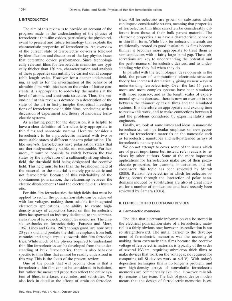
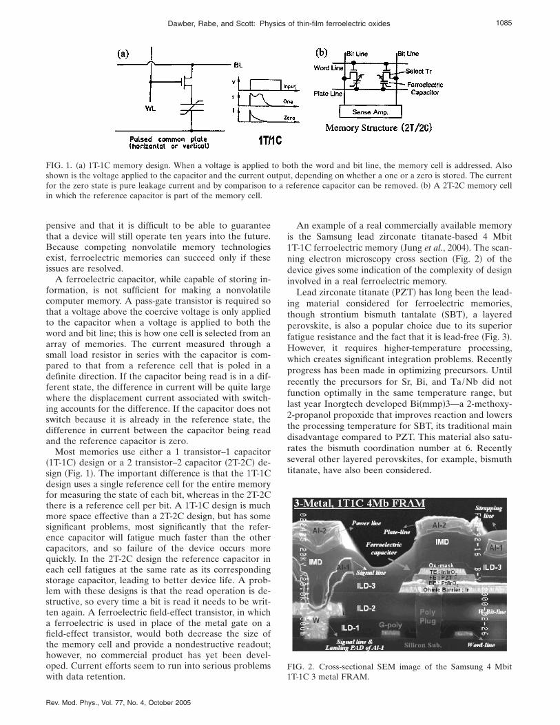
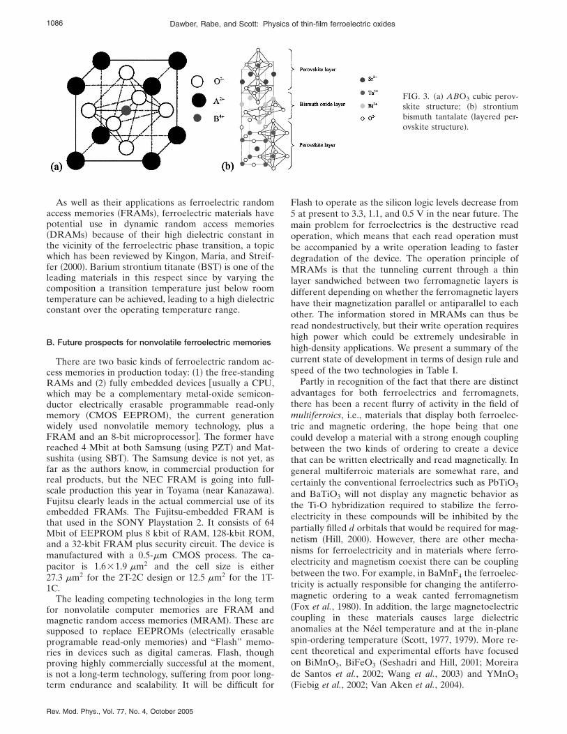

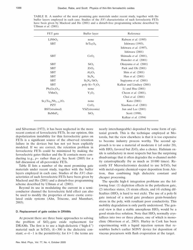
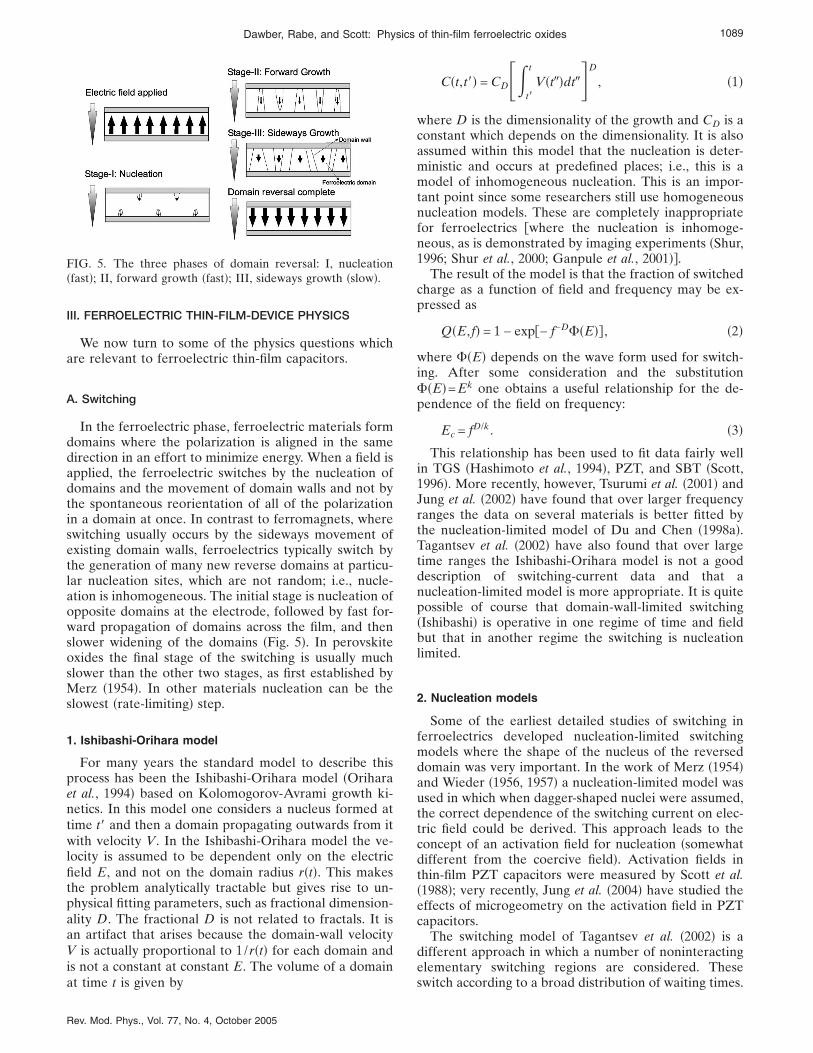

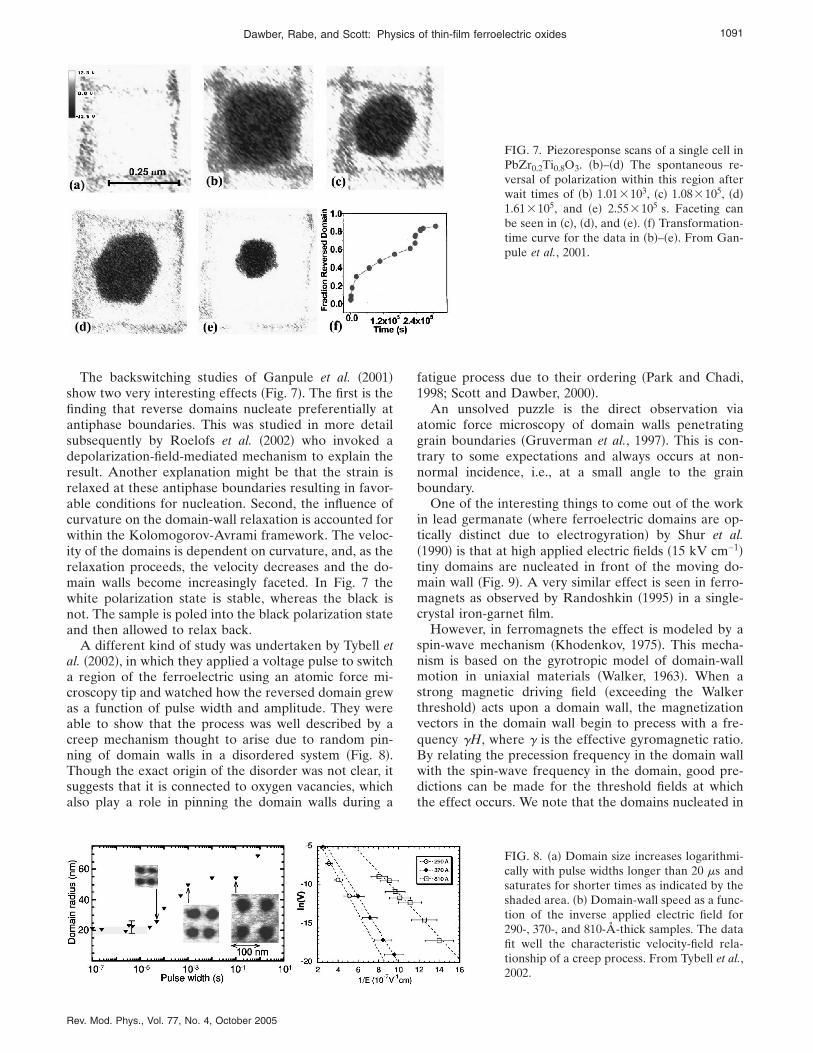


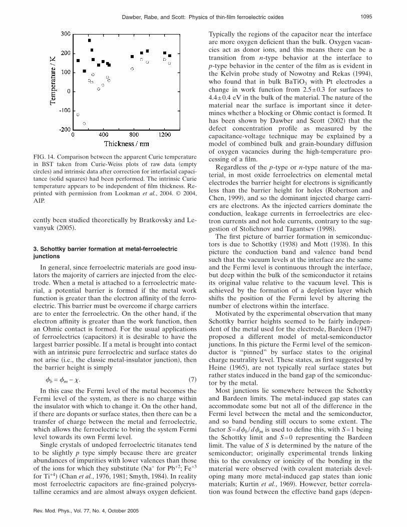


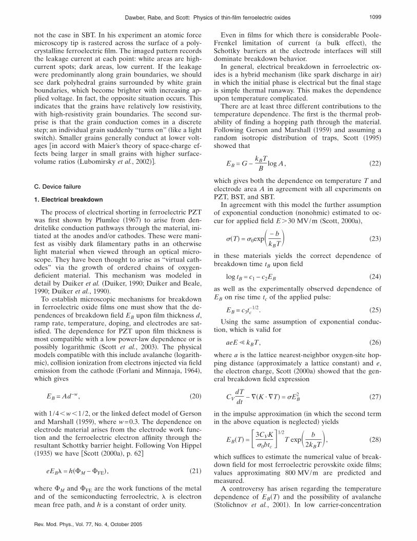
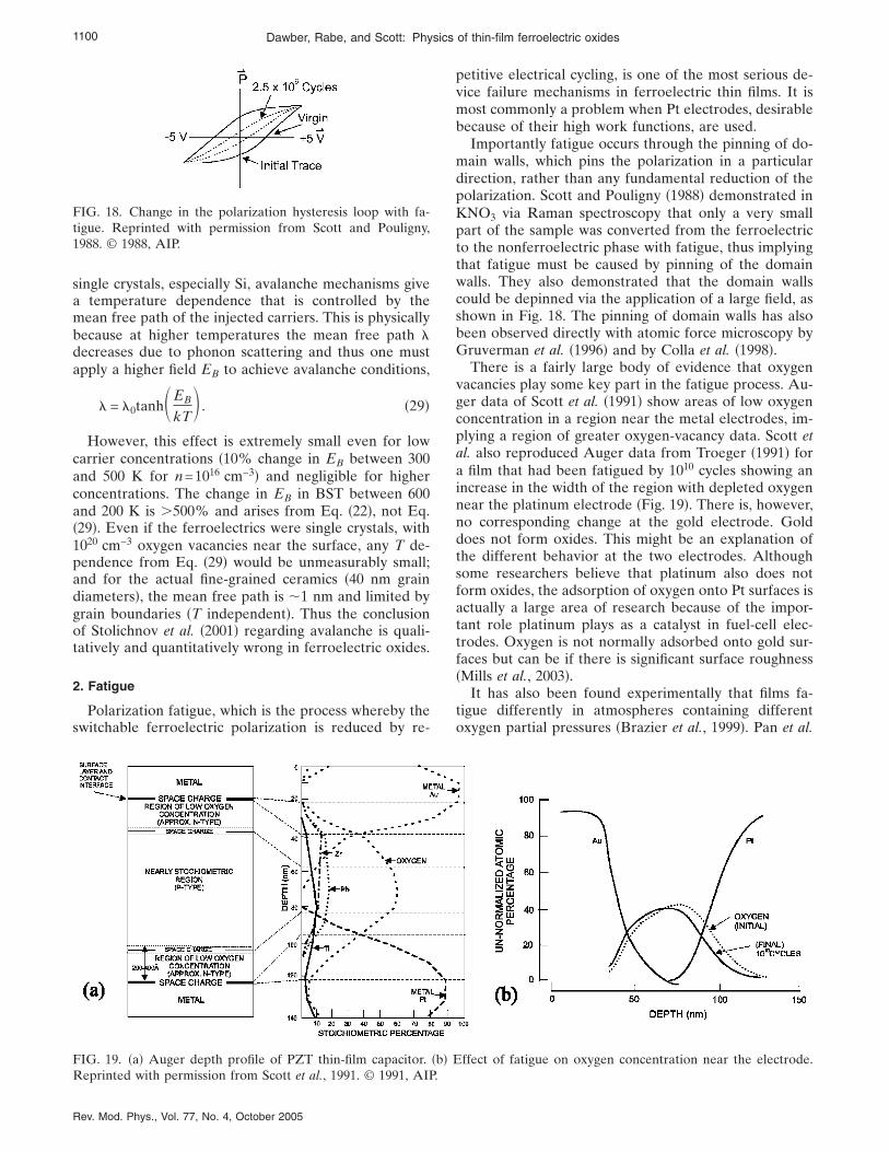


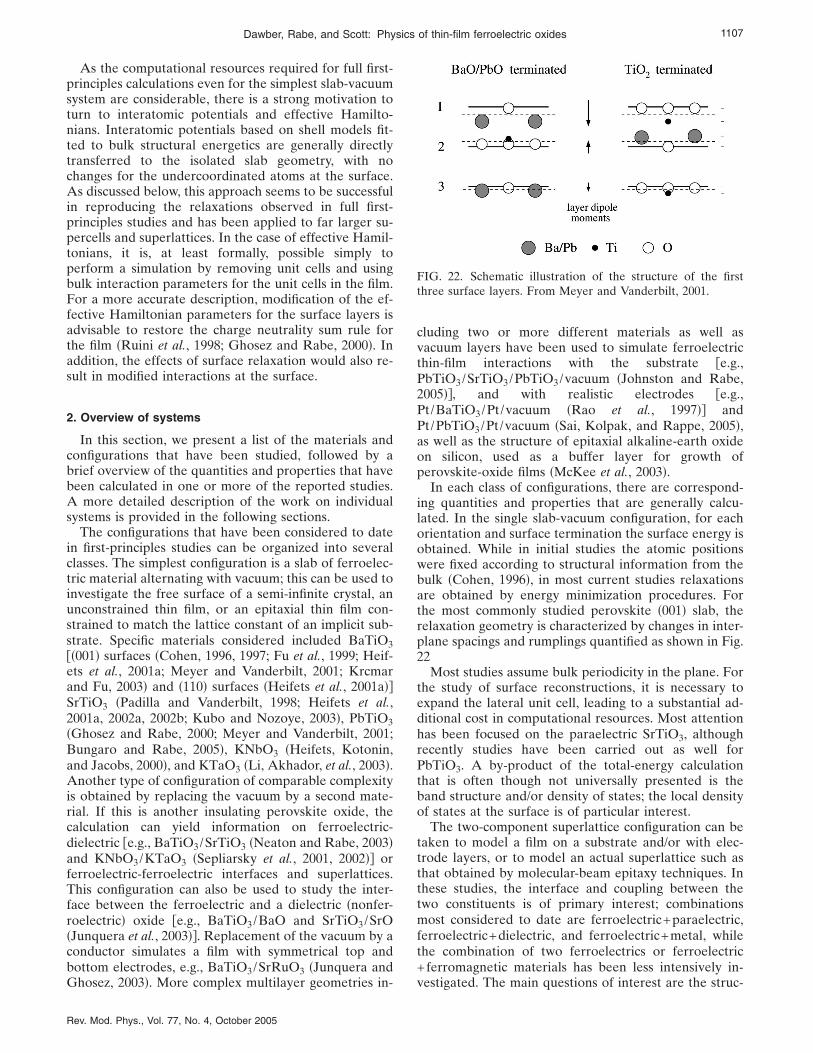

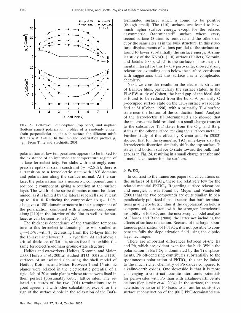

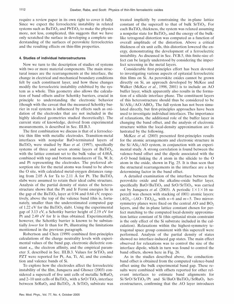
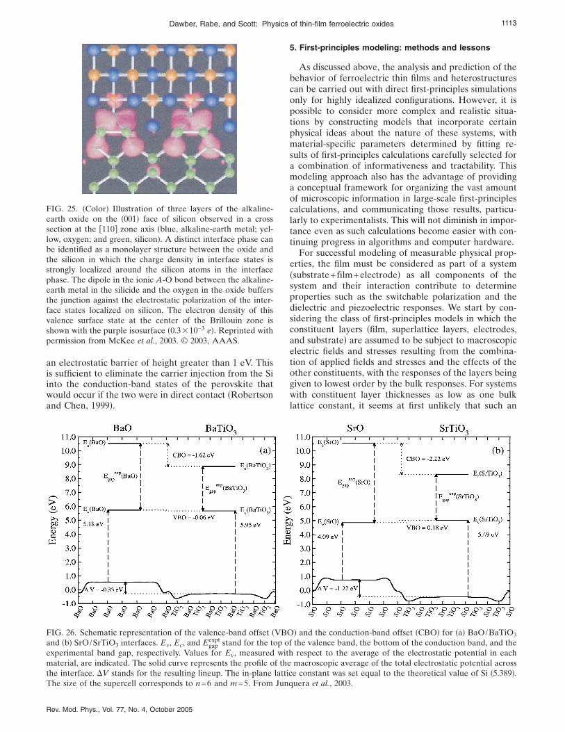
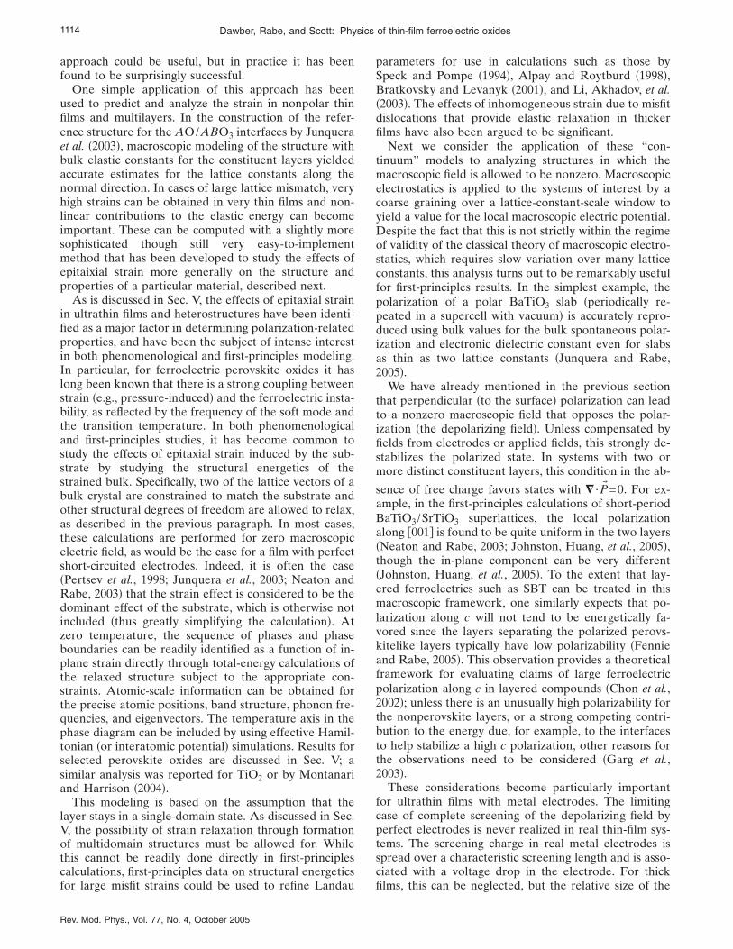

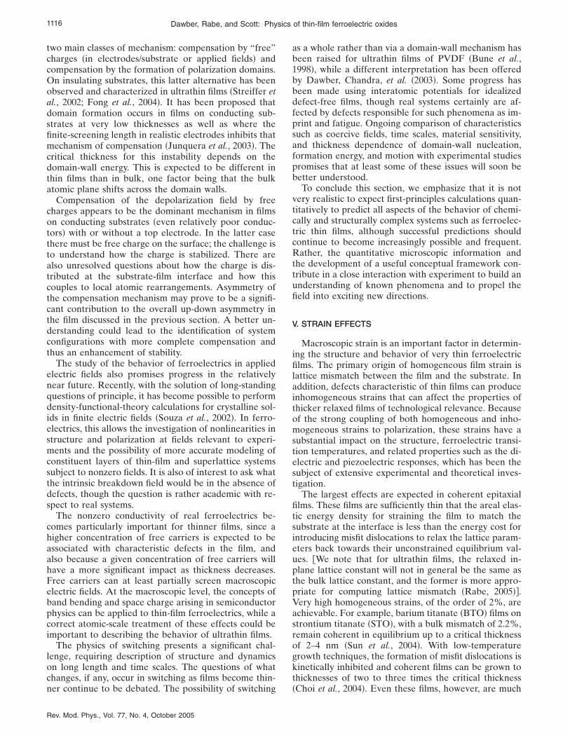

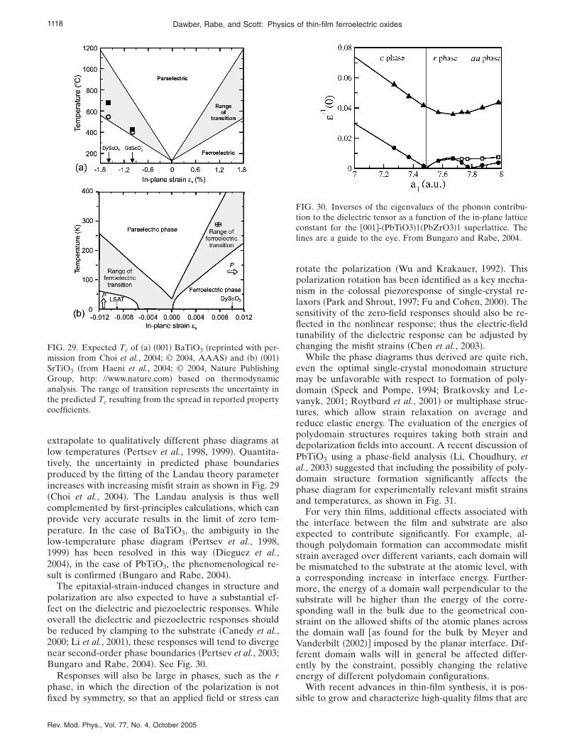

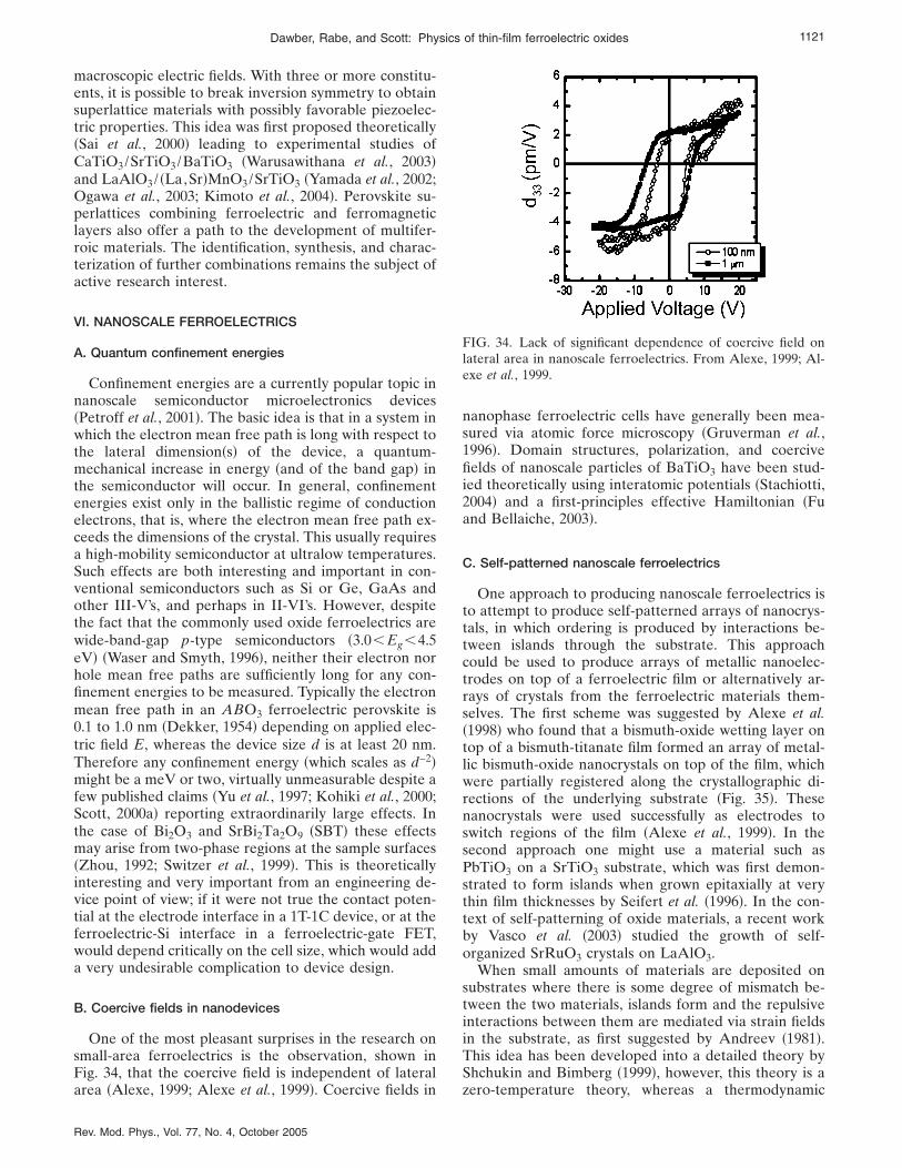

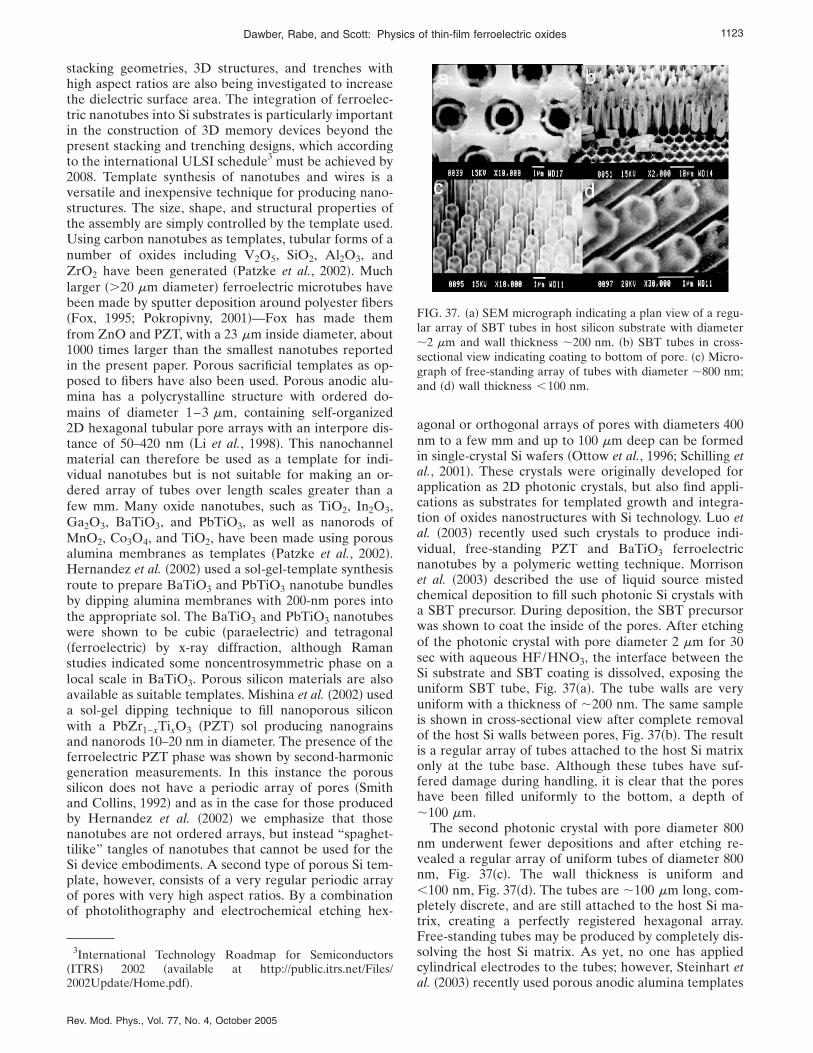
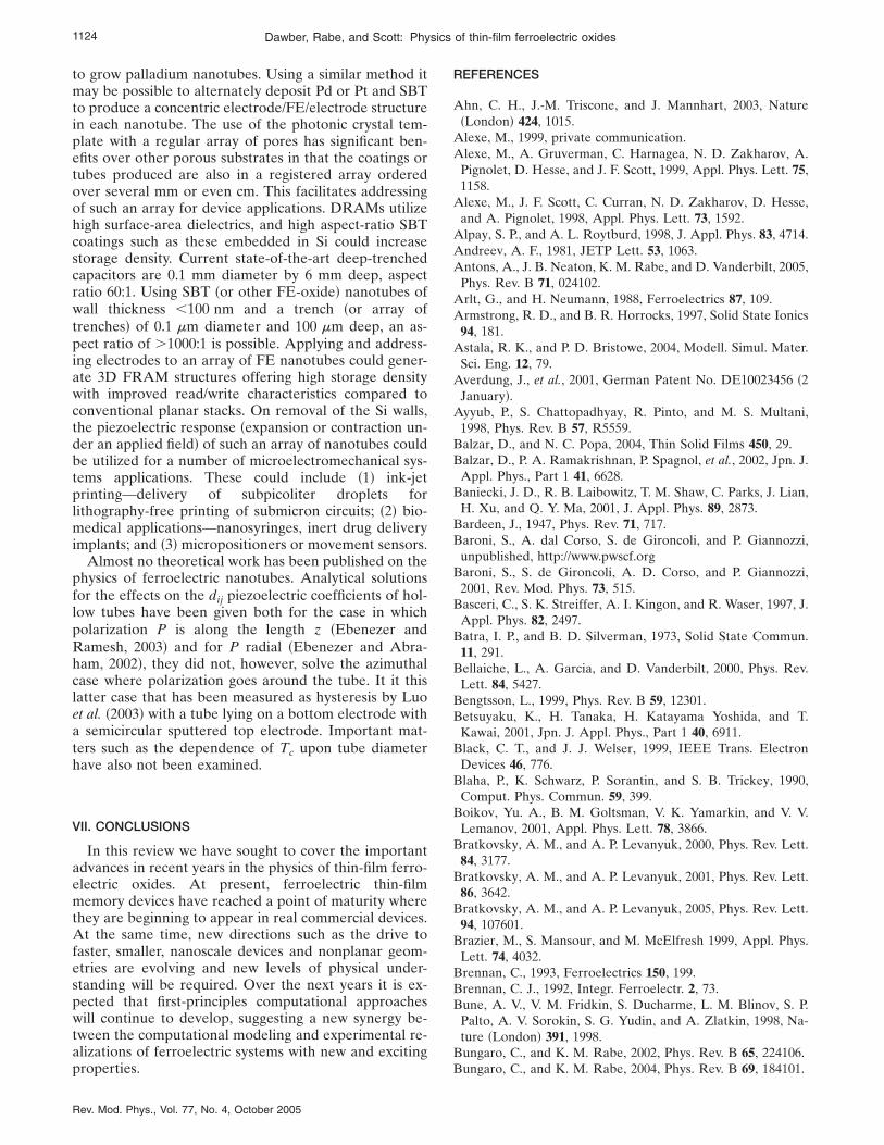


![FERROELECTRIC RAM [FRAM]](https://static.documents.pub/doc/80x56/56816799550346895ddcd567/ferroelectric-ram-fram.jpg)
![Sangeetha [Ferroelectric Memory]](https://static.documents.pub/doc/80x56/55cf8f91550346703b9d9665/sangeetha-ferroelectric-memory.jpg)


