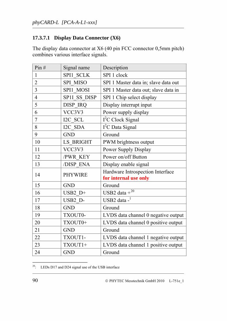
List of Figures..............................................................................................iii List of Tables ............................................................................................... iv Conventions, Abbreviations and Acronyms............................................vii Preface.......................................................................................................... ix 1 Introduction......................................................................................... 1
1.1 Block Diagram ............................................................................. 4 1.2 View of the phyCARD-L ............................................................. 5 1.3 Minimum Requirements to Operate the phyCARD-L................. 7
4.1 Primary System Power (VDD_3V3).......................................... 23 4.2 Standby Voltage (VSTBY) ........................................................ 24 4.3 On-board Voltage Regulator (U1).............................................. 24 4.4 Supply Voltage for external Logic ............................................. 26
5 Power Management .......................................................................... 27 6 System Configuration and Booting ................................................. 29 7 System Memory................................................................................. 31
13 LVDS Camera Interface .................................................................. 57 13.1 Signal configuration (J6)............................................................ 58
14 Technical Specifications ................................................................... 59 15 Component Placement Diagram ..................................................... 63 16 Hints for Integrating and Handling the phyCARD-L................... 65
16.1 Integrating the phyCARD-M ..................................................... 65 16.2 Handling the phyCARD-L......................................................... 67
17 The phyCARD-L on the phyBASE ................................................. 69 17.1 Concept of the phyBASE Board ................................................ 70 17.2 Overview of the phyBASE Peripherals ..................................... 71
List of Figures Figure 1: Block Diagram of the phyCARD-L ........................................... 4
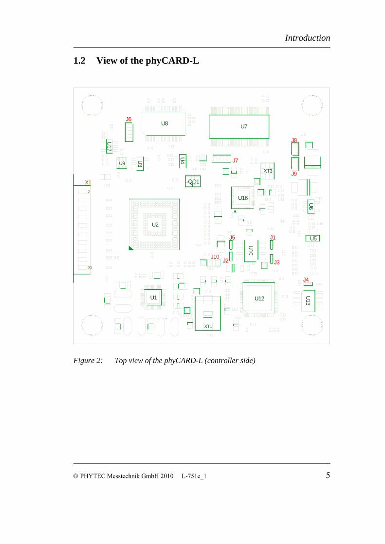
Figure 2: Top view of the phyCARD-L (controller side).......................... 5
Figure 3: Bottom view of the phyCARD-L (connector side).................... 6
Figure 4: Pinout of the phyCARD-Connector (top view, with cross section insert) ........................................................................... 10
Figure 5: Typical jumper pad numbering scheme ................................... 17
List of Tables Table 1: Abbreviations and Acronyms used in this Manual................. viii Table 2: X-Arc Bus pinout..................................................................... 12
Table 3: Pinout of the phyCARD-Connector X2................................... 16
This hardware manual describes the PCA-A-L1 Single Board Computer in the following referred to as phyCARD-L. The manual specifies the phyCARD-L's design and function. Precise specifications for the Texas Instruments OMAP35x microcontrollers can be found in the enclosed microcontroller Data Sheet/User's Manual. Conventions The conventions used in this manual are as follows: Signals that are preceded by a "n", "/", or “#”character (e.g.: nRD,
/RD, or #RD), or that have a dash on top of the signal name (e.g.: RD) are designated as active low signals. That is, their active state is when they are driven low, or are driving low.
A "0" indicates a logic zero or low-level signal, while a "1" represents a logic one or high-level signal.
Tables which describe jumper settings show the default position in bold, blue text.
Text in blue italic indicates a hyperlink within, or external to the document. Click these links to quickly jump to the applicable URL, part, chapter, table, or figure.
References made to the phyCARD-Connector always refer to the high density molex connector on the undersides of the phyCARD-L Single Board Computer.
Abbreviations and Acronyms Many acronyms and abbreviations are used throughout this manual. Use the table below to navigate unfamiliar terms used in this document. Abbreviation Definition BSP Board Support Package (Software delivered with the
Development Kit including an operating system (Windows, or Linux) preinstalled on the module and Development Tools).
CB Carrier Board; used in reference to the phyBASE Development Kit Carrier Board.
Abbreviation Definition DFF D flip-flop. EMB External memory bus. EMI Electromagnetic Interference. GPI General purpose input. GPIO General purpose input and output. GPO General purpose output. IRAM Internal RAM; the internal static RAM on the Texas
Instruments OMAP35x microcontroller. J Solder jumper; these types of jumpers require solder
equipment to remove and place. JP Solderless jumper; these types of jumpers can be
removed and placed by hand with no special tools. PCB Printed circuit board. PEB PHYTEC Extension Board POR Power-on reset RTC Real-time clock. SBC Single Board Computer; used in reference to the
PCA-A-L1 /phyCARD-A-L1 Single Board Computer
SMT Surface mount technology. Sx User button Sx (e.g. S1, S2, etc.) used in reference to
the available user buttons, or DIP-Switches on the Carrier Board.
Sx_y Switch y of DIP-Switch Sx; used in reference to the DIP-Switch on the Carrier Board.
VSTBY SBC standby voltage input Table 1: Abbreviations and Acronyms used in this Manual
Note: The BSP delivered with the phyCARD-L usually includes drivers and/or software for controlling all components such as interfaces, memory, etc.. Therefore programming close to hardware at register level is not necessary in most cases. For this reason, this manual contains no detailed description of the controller's registers, or information relevant for software development. Please refer to the OMAP35x Reference Manual, if such information is needed to connect customer designed applications.
As a member of PHYTEC's new phyCARD product family the phyCARD-L is one of a series of PHYTEC Single Board Computers (SBCs) that can be populated with different controllers and, hence, offers various functions and configurations. PHYTEC supports a variety of 8-/16- and 32-bit controllers in two ways: (1) as the basis for Rapid Development Kits which serve as a
reference and evaluation platform (2) as insert-ready, fully functional phyCARD OEM modules,
which can be embedded directly into the user’s peripheral hardware design.
Implementation of an OEM-able SBC subassembly as the "core" of your embedded design allows you to focus on hardware peripherals and firmware without expending resources to "re-invent" microcontroller circuitry. Furthermore, much of the value of the phyCARD module lies in its layout and test. PHYTEC's new phyCARD product family consists of a series of extremely compact embedded control engines featuring various processing performance classes while using the newly developed X-Arc embedded bus standard. The standardized connector footprint and pin assignment of the X-Arc bus makes this new SBC generation extremely scalable and flexible. This also allows to use the same carrier board to create different applications depending on the required processing power. With this new SBC concept it is possible to design entire embedded product families around vastly different processor performances while optimizing overall system cost. In addition, future advances in processor technology are already considered with this new embedded bus standard making product upgrades very easy. Another major advantage is the forgone risk of potential system hardware redesign steps caused by processor or other critical component discontinuation. Just use one of PHYTEC's other phyCARD SBCs thereby ensuring an extended product life cycle of your embedded application.
phyCARD-L [PCA-A-L1-xxx]
Production-ready Board Support Packages (BSPs) and Design Services for our hardware will further reduce your development time and risk and allow you to focus on your product expertise. Take advantage of PHYTEC products to shorten time-to-market, reduce development costs, and avoid substantial design issues and risks. With this new innovative full system solution you will be able to bring your new ideas to market in the most timely and cost-efficient manner. For more information go to: http://www.phytec.com/services/
Ordering Information
The part numbering of the phyCARD has the following structure: PCA-A-L1-xxxxxx Generation A = First generation
Performance class S = small M = middle L = large XL = largest
Controller No. of specified performance class
Assembly options (depending on model) In order to receive product specific information on changes and updates in the best way also in the future, we recommend to register at http://www.phytec.de/de/support/registrierung.html You can also get technical support and additional information concerning your product.
The support section of our web site provides product specific information, such as errata sheets, application notes, FAQs, etc. http://www.phytec.de/de/support/faq/faq-phyCARD-L.html Declaration of Electro Magnetic Conformity of the PHYTEC phyCARD-L PHYTEC Single Board Computers (henceforth products) are designed for installation in electrical appliances or as dedicated Evaluation Boards (i.e.: for use as a test and prototype platform for hardware/software development) in laboratory environments. Caution: PHYTEC products lacking protective enclosures are subject to damage by ESD and, hence, may only be unpacked, handled or operated in environments in which sufficient precautionary measures have been taken in respect to ESD-dangers. It is also necessary that only appropriately trained personnel (such as electricians, technicians and engineers) handle and/or operate these products. Moreover, PHYTEC products should not be operated without protection circuitry if connections to the product's pin header rows are longer than 3 m. PHYTEC products fulfill the norms of the European Union’s Directive for Electro Magnetic Conformity only in accordance to the descriptions and rules of usage indicated in this hardware manual (particularly in respect to the pin header row connectors, power connector and serial interface to a host-PC). Implementation of PHYTEC products into target devices, as well as user modifications and extensions of PHYTEC products, is subject to renewed establishment of conformity to, and certification of, Electro Magnetic Directives. Users should ensure conformance following any modifications to the products as well as implementation of the products into target systems.
The phyCARD-L belongs to PHYTEC’s phyCARD Single Board Computer module family. The phyCARD SBCs represent the continuous development of PHYTEC Single Board Computer technology. Like its mini-, micro- and nanoMODUL predecessors, the phyCARD boards integrate all core elements of a microcontroller system on a subminiature board and are designed in a manner that ensures their easy expansion and embedding in peripheral hardware developments. PHYTEC's phyCARD family introduces the newly developed X-Arc embedded bus standard. Apart from processor performance, a large number of embedded solutions require a corresponding number of standard interfaces. Among these process interfaces are for example Ethernet, USB, UART, SPI, I2C, audio, display and camera connectivity. The X-Arc bus exactly meets this requirement. As well the location of the commonly used interfaces as the mechanical specifications are clearly defined. All interface signals of PHYTEC's new X-Arc bus are available on a single, 100-pin , high-density pitch (0.635 mm) connector, allowing the phyCARDs to be plugged like a "big chip" into a target application. The reduced complexity of the phyCARD SBC as well as the smaller number of interface signals greatly simplifies the SBC carrier board design helping you to reduce your time-to-market. As independent research indicates that approximately 70 % of all EMI (Electro Magnetic Interference) problems stem from insufficient supply voltage grounding of electronic components in high frequency environments approximately 20 % of all pin header connectors on the X-Arc bus are dedicated to Ground. This improves EMI and EMC characteristics and makes it easier to design complex applications meeting EMI and EMC guidelines using phyCARD boards even in high noise environments.
phyCARD boards achieve their small size through modern SMD technology and multi-layer design. In accordance with the complexity of the module, 0402-packaged SMD components and laser-drilled microvias are used on the boards, providing phyCARD users with access to this cutting edge miniaturization technology for integration into their own design. The phyCARD-L is a subminiature (60 x 60 mm) insert-ready Single Board Computer populated with the Texas Instruments OMAP35x microcontroller. Its universal design enables its insertion in a wide range of embedded applications. Precise specifications for the controller populating the board can be found in the applicable controller Reference Manual or datasheet. The descriptions in this manual are based on the Texas Instruments OMAP35x. No description of compatible microcontroller derivative functions is included, as such functions are not relevant for the basic functioning of the phyCARD-L. The phyCARD-L offers the following features: • Subminiature Single Board Computer (´60 x 60 mm) achieved
through modern SMD technology • Populated with the Texas Instruments OMAP35x microcontroller
(CBB package with 515 balls and package-on-package (PoP) memory option)
• Improved interference safety achieved through multi-layer PCB technology and dedicated ground pins
• X-Arc bus including commonly used interfaces such as Ethernet, USB, UART, SPI, I2C, audio, display and camera connectivity (both LVDS) available at one 100-pin high-density (0.635 mm) Molex connector, enabling the phyCARD-L to be plugged like a "big chip" into target application
• Max. 600 MHz core clock frequency • Boot from NAND Flash • PoP memory device with 256 MByte NAND Flash1 and
256 MByte LP DDR SDRAM
1 Please contact PHYTEC for more information about additional module configurations.
• alternatively up to 1 GByte NAND Flash (VFBGA) • 4KB (up to 32kB) I2C EEPROM • Serial interface with 4 lines (TTL) allowing simple hardware
handshake • High-Speed USB OTG transceiver • High-Speed USB HOST transceiver • Auto HDX/FDX 10/100MBit Ethernet interface, with HP Auto
MDI/MDI-X support • Additional 1 Kbit EEPROM connected to the Ethernet controller
to store MAC-address • Single supply voltage of 3.3V (max 1.5 A) with on-board power
management All controller required supplies generated on board • All controller required supplies generated on board • 4 Channel LVDS (24Bit) LCD-Interface • Support of standard 20 pin debug interface through JTAG
connector • One I2C interfaces • One SPI interfaces • SD/MMC card interface with DMA • SSI Interface (AC'97)1 • LVDS Camera Interface • 3 GPIO/IRQ ports • 2 Power State outputs to support applications requiring a power
management • 1 Wake Up input
1: the OMAP35x does not feature an AC'97 interface. The AC'97 interface of the phyCARD-L
is emulated with the multi-channel buffered Serial Port (McBSP). Thus it is only available with the BSP coming with the phyCARD-L
Basic operation of the phyCARD-L only requires supply of a +3V3 input voltage with 1.5 A load and the corresponding GND connection. These supply pins are located at the phyCARD-Connector X2: VDD_3V3: X2 1A, 2A, 3A, 1B, 2B, 3B Connect all +3.3V VCC input pins to your power supply and at least the matching number of GND pins. Corresponding GND: X2 4A, 8A, 13A, 4B, 8B, 13B Please refer to section 2 for information on additional GND Pins located at the phyCARD-Connector X2. Caution: We recommend connecting all available +3V3 input pins to the power supply system on a custom carrier board housing the phyCARD-L and at least the matching number of GND pins neighboring the +3V3 pins. In addition, proper implementation of the phyCARD-L module into a target application also requires connecting all GND pins neighboring signals that are being used in the application circuitry. Please refer to section 4 for more information.
Please note that all module connections are not to exceed their expressed maximum voltage or current. Maximum signal input values are indicated in the corresponding controller manuals/data sheets. As damage from improper connections varies according to use and application, it is the user's responsibility to take appropriate safety measures to ensure that the module connections are protected from overloading through connected peripherals. As Figure 4 indicates, all X-Arc bus signals extend to one surface mount technology (SMT) connector (0.635 mm) lining on side of the module (referred to as phyCARD-Connector). This allows the phyCARD-L to be plugged into any target application like a "big chip". The numbering scheme for the phyCARD-Connector is based on a two dimensional matrix in which column positions are identified by a letter and row position by a number. Pin 1A, for example, is always located in the upper left hand corner of the matrix. The pin numbering values increase moving down on the board. Lettering of the pin connector rows progresses alphabetically from left to right (refer to Figure 4). The numbered matrix can be aligned with the phyCARD-L (viewed from above; phyCARD-Connector pointing down) or with the socket of the corresponding phyCARD Carrier Board/user target circuitry. The upper left-hand corner of the numbered matrix (pin 1A) is thus covered with the corner of the phyCARD-L marked with "1A". The numbering scheme is always in relation to the PCB as viewed from above, even if all connector contacts extend to the bottom of the module. The numbering scheme is thus consistent for both the module’s phyCARD-Connector as well as the mating connector on the phyBASE Carrier Board or target hardware, thereby considerably reducing the risk of pin identification errors.
phyCARD-L [PCA-A-L1-xxx]
Since the pins are exactly defined according to the numbered matrix previously described, the phyCARD-Connector is usually assigned a single designator for its position (X1 for example). In this manner the phyCARD-Connector comprises a single, logical unit regardless of the fact that it could consist of more than one physical socketed connector.
4: Pinout of the phyCARD-Connector (top view, with cross section
The following figure illustrates the numbered matrix system. It shows a phyCARD-L with SMT phyCARD-Connectors on its underside (defined as dotted lines) mounted on a Carrier Board. In order to facilitate understanding of the pin assignment scheme, the diagram presents a cross-view of the phyCARD-module showing these phyCARD-Connectors mounted on the underside of the module’s
Table 2 shows the pinout of the X-Arc bus with the functional grouping of the signals, while Table 3 provides an overview of the pinout of the phyCARD-Connector with signal names and descriptions specific to the phyCARD-L. It also provides the appropriate signal level interface voltages listed in the SL (Signal Level) column and the signal direction. The Texas Instruments OMAP35x is a multi-voltage operated microcontroller and as such special attention should be paid to the interface voltage levels to avoid unintentional damage to the microcontroller and other on-board components. Please refer to the Texas Instruments OMAP35x Reference Manual for details on the functions and features of controller signals and port pins.
Signal Pin Pin Signal I/O In VCC 1A 1B VCC In In VCC 2A 2B VCC In In VCC 3A 3B VCC In - GND 4A 4B GND - Out VCC_LOGIC 5A 5B VCC_LOGIC Out - FEEDBACK 6A 6B VSTBY In In nRESET_IN 7A 7B nRESET_OUT Out - GND 8A 8B GND - Out LVDS_TX0+ 9A 9B LVDS_TX1+ Out Out LVDS_TX0- 10A 10B LVDS_TX1- Out Out LVDS_TX2+ 11A 11B LVDS_TX3+ Out Out LVDS_TX2- 12A 12B LVDS_TX3- Out - GND 13A 13B GND - Out LVDS_TXCLK+ 14A 14B LVDS_CAM_RX+ In Out LVDS_TXCLK- 15A 15B LVDS_CAM_RX- In Out LVDS_CAM_MCLK 16A 16B LVDS_CAM_nLOCK Out Bi I2C_CLK 17A 17B I2C_DATA Bi - GND 18A 18B GND - Out ETH_SPEED 19A 19B ETH_LINK Out Out ETH_TX+ 20A 20B ETH_RX+ In Out ETH_TX- 21A 21B ETH_RX- In - GND 22A 22B GND - Out USB_OTG_PWR1 23A 23B USB_PWR2 Out In USB_OTG_OC1 24A 24B USB_OC2 In - GND 25A 25B GND - Bi USB_OTG_VBUS1 26A 26B nSuspend_to_RAM Out Bi USB_OTG_D1- 27A 27B USB_D2- Bi Bi USB_OTG_D1+ 28A 28B USB_D2+ Bi In USB_OTG_UID1 29A 29B nPower_Off Out - GND 30A 30B GND - Bi SDIO_D0 31A 31B SDIO_D1 Bi Bi SDIO_D2 32A 32B SDIO_D3 Bi Out SDIO_CLK 33A 33B SDIO_CMD Bi - GND 34A 34B GND - Out SPI_CS0 35A 35B SPI_CS1 Out In SPI_RDY 36A 36B SPI_MOSI Out Out SPI_CLK 37A 37B SPI_MISO In - GND 38A 38B GND - Out UART_TXD 39A 39B UART_RXD In In UART_RTS 40A 40B UART_CTS Out - GND 41A 41B GND - Bi HDA_SEL/AC97_INT 42A 42B AC97/HDA_BIT_CLK Bi Out AC97/HDA_SDATA_OUT 43A 43B AC97/HDA_SYNC Out In AC97/HDA_SDATA_IN 44A 44B AC97/HDA_nRESET Out - GND 45A 45B GND - Bi GPIO0/IRQ0 46A 46B SDIO_CD In Bi GPIO2/IRQ2/PWM 47A 47B GPIO1/IRQ1 Bi In nWKUP 48A 48B for internal use only Bi - GND 49A 49B GND - In CONFIG0 50A 50B CONFIG1 In
Note: SL is short for Signal Level (V) and is the applicable logic level to interface a given pin. Those pins marked as “N/A” have a range of applicable values that constitute proper operation. Please refer to the phyCARD Design-In Guide (LAN-051) for layout recommendations and example circuitry. Pin Row X2A Pin # Signal I/O SL Description
1A VDD_3V3 I Power 3.3V Primary Voltage Supply Input 2A VDD_3V3 I Power 3.3V Primary Voltage Supply Input 3A VDD_3V3 I Power 3.3V Primary Voltage Supply Input 4A GND - - Ground 0V 5A VDD_IO O Power VCC Logic Output 6A X_FEEDBACK O Power Feedback Output to indicate the
supply voltage required (3V3 or 5V) 7A X_nRESET_IN I VCC_LOGIC Active low Reset In 8A GND - Power Ground 0V 9A X_DIS_LVDS_TX0+ O LVDS LVDS Chanel 0 positive Output 10A X_DIS_LVDS_TX0- O LVDS LVDS Chanel 0 negative Output 11A X_DIS_LVDS_TX2+ O LVDS LVDS Chanel 2 positive Output 12A X_DIS_LVDS_TX2- O LVDS LVDS Chanel 2 negative Output 13A GND - Power Ground 0V 14A X_DIS_LVDS_TXCLK+ O LVDS LVDS Clock positive Output 15A X_DIS_LVDS_TXCLK- O LVDS LVDS Clock negative output 16A X_CAM_LVDS_MCLK O VCC3V3 Clock Output for Camera Interface 17A X_I2C_SCL O VCC_LOGIC I2C Clock Output 18A GND - Power Ground 0V 19A X_ETH_SPEED O VCC3V3 Ethernet Speed Indicator (Open Drain)20A X_ETH_TX+ O (I) VCC3V3 Transmit positive output (normal)
27A X_USBOTG_DM I/O USB transceiver cable interface, D- 28A X_USBOTG_DP I/O USB transceiver cable interface, D+ 29A X_USBOTG_UID I USB on the go transceiver cable ID
resistor connection 30A GND - Power Ground 0V 31A X_SDIO_D0 I/O VCC_LOGIC SD/MMC Data line both in 1-bit and
4-bit mode 32A X_SDIO_D2 I/O VCC_LOGIC SD/MMC Data line both in 1-bit and
4-bit mode 33A X_SDIO_CLK O VCC_LOGIC SD/MMC Clock for MMC/SD/SDIO 34A GND - Power Ground 0V 35A X_SPI_CS0 O VCC_LOGIC SPI Chip select 0 36A X_SPI_RDY O VCC_LOGIC SPI Data ready in Master mode 37A X_SPI_CLK O VCC_LOGIC SPI Clock 38A GND - Power Ground 0V 39A X_UART_TXD O VCC_LOGIC Serial transmit signal UART 40A X_UART_RTS O VCC_LOGIC Request to send UART 41A GND - Power Ground 0V 42A X_AC97/HDA_INT/SEL I/O- VCC_LOGIC AC'971 Interrupt Input 43A X_AC97/HDA_SDOUT O VCC_LOGIC AC'971 Transmit Output 44A X_AC97/HDA_SDIN I VCC_LOGIC AC'971 Receive Input 45A GND - Power Ground 0V 46A X_GPIO0/IRQ0 I/O VCC_LOGIC GPIO0/IRQ0 (µC port GPIO_144
(GPIO_1512)) 47A X_GPIO2/IRQ2/PWM
I/O VCC_LOGIC GPIO2/IRQ2/PWM (µC port
GPIO_147 (GPIO_1462)) 48A X_nWKUP I VCC_LOGIC Wakeup Interrupt Input (µC port
GPIO_146 (GPIO_272)) 49A GND - Power Ground 0V 50A X_CONFIG0 I VCC_LOGIC Boot-Mode Input 0
1: the OMAP35x does not feature an AC'97 interface. The AC'97 interface of the phyCARD-L
is emulated with the multi-channel buffered Serial Port (McBSP). Thus it is only available with the BSP coming with the phyCARD-L
2 : can be selected by jumper (refer to section 3)
1B VCC_3V3 - Power 3.3V Primary Voltage Supply Input 2B VCC_3V3 - Power 3.3V Primary Voltage Supply Input 3B VCC_3V3 - Power 3.3V Primary Voltage Supply Input 4B GND - Power Ground 0V 5B VDD_IO O Power VCC Logic Output 6B VSTBY - Power Standby Voltage Input 7B X_nRESET_OUT - VCC_LOGIC Active low Reset output 8B GND - Power Ground 0V 9B X_DIS_LVDS_TX1+ O LVDS LVDS Chanel 1 positive Output 10B X_DIS_LVDS_TX1- O LVDS LVDS Chanel 1 negative Output 11B X_DIS_LVDS_TX3+ O LVDS LVDS Chanel 3 positive Output 12B X_DIS_LVDS_TX3- O LVDS LVDS Chanel 3 negative Output 13B GND - Power Ground 0V 14B X_CAM_LVDS_RX+ O LVDS LVDS Receive positive Input for
Camera 15B X_CAM_LVDS_RX- O LVDS LVDS Receive negative Input for
Camera 16B X_CAM_LVDS_nLOCK O VCC3V3 Lock Output for Camera Interface 17B X_I2C_SDA I/O VCC_LOGIC I2C Data 18B GND - Power Ground 0V 19B X_ETH_LINK O VCC3V3 Ethernet Link Indicator (Open Drain) 20B X_ETH_RX+ I (O) VCC3V3 Receive positive input (normal)
32B X_SDIO_D3 I/O VCC_LOGIC SD/MMC Data line both in 1-bit and 4-bit mode
33B X_SDIO_CMD O VCC_LOGIC SD/MMC Command for MMC/SD/SDIO
34B GND - Power Ground 0V 35B X_SPI_CS1 O VCC_LOGIC SPI Chip select 1 36B X_SPI_MOSI I/O VCC_LOGIC SPI Master data out; slave data in 37B X_SPI_MISO I/O VCC_LOGIC SPI Master data in; slave data out 38B GND - Power Ground 0V 39B X_UART_RXD I VCC_LOGIC Serial data receive signal UART 40B X_UART_CTS I VCC_LOGIC Clear to send UART 41B GND - Power Ground 0V 42B X_AC97/HDA_BITCLK I/O VCC_LOGIC AC'971 Clock 43B X_AC97/HDA_SYNC O VCC_LOGIC AC'971 SYNC 44B X_AC97/HDA_nRST O VCC_LOGIC AC'971 Reset 45B GND - Power Ground 0V 46B X_SDIO_CD I VCC_LOGIC SD/MMC Card Detect for
MMC/SD/SDIO (µC port GPIO_126) 47B X_GPIO1/IRQ1 I/O VCC_LOGIC GPIO1/IRQ1 (µC port GPIO_145
for internal use only 49B GND - Power Ground 0V 50B X_CONFIG1 I VCC_LOGIC Boot-Mode Input 1
Table 3: Pinout of the phyCARD-Connector X2
1: the OMAP35x does not feature an AC'97 interface. The AC'97 interface of the phyCARD-L
is emulated with the multi-channel buffered Serial Port (McBSP). Thus it is only available with the BSP coming with the phyCARD-L
2 : can be selected by jumper (refer to section 3)
Jumpers
3 Jumpers
For configuration purposes, the phyCARD-L has 14 solder jumpers, some of which have been installed prior to delivery. Figure 5 illustrates the numbering of the solder jumper pads, while Figure 6 and Figure 7 indicate the location of the solder jumpers on the board. 10 solder jumpers are located on the top side of the module (opposite side of connectors) and 4 solder jumpers are located on the bottom side of the module (connector side). Table 4 below provides a functional summary of the solder jumpers which can be changed to adapt the phyCARD-L to your needs. It shows their default positions, and possible alternative positions and functions. A detailed description of each solder jumper can be found in the applicable chapter listed in the table. Note: Jumpers not listed should not be changed as they are installed with regard to the configuration of the phyCARD-L.
e.g.: J9 e.g.: J2
Figure 5: Typical jumper pad numbering scheme
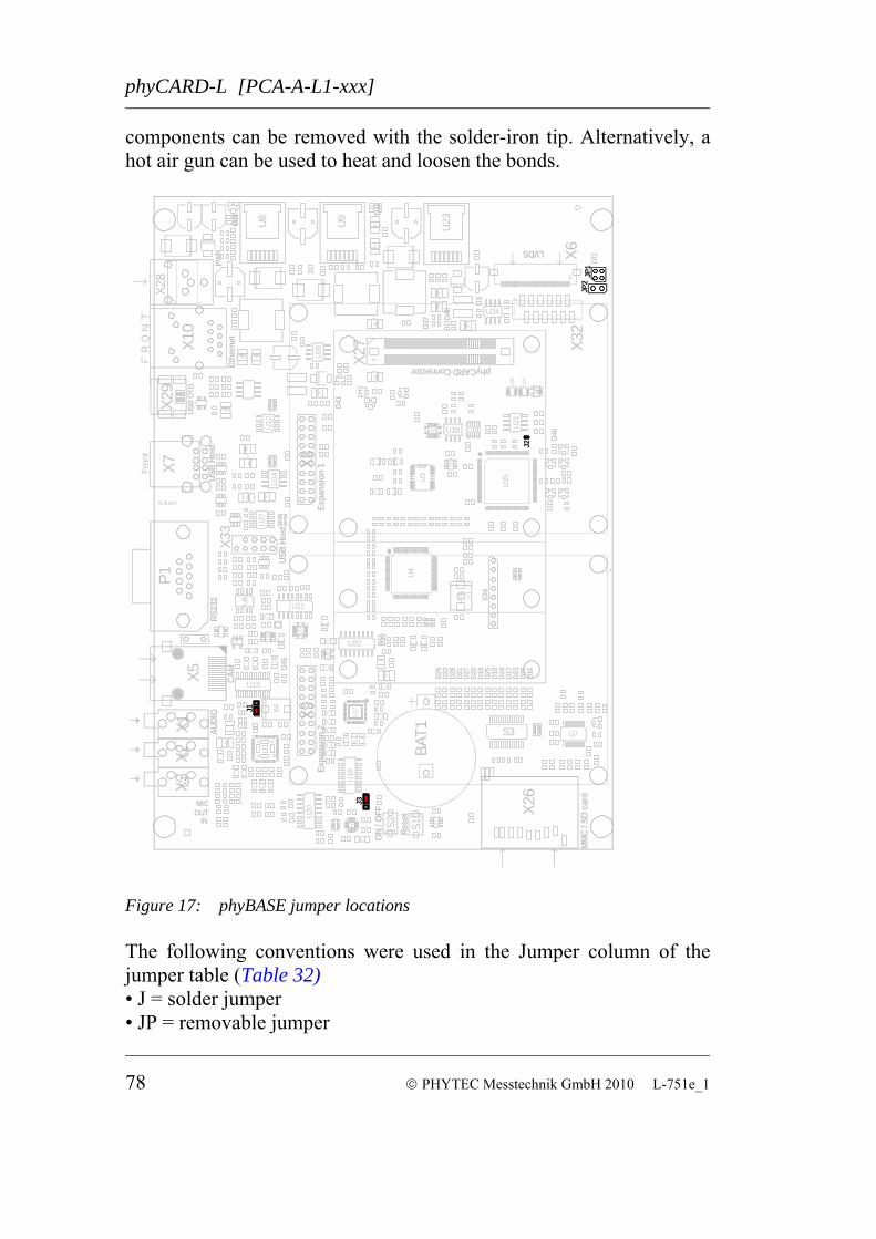
If manual jumper modification is required please ensure that the board as well as surrounding components and sockets remain undamaged while de-soldering. Overheating the board can cause the solder pads to loosen, rendering the module inoperable. Carefully heat neighboring connections in pairs. After a few alternations, components can be removed with the solder-iron tip. Alternatively, a hot air gun can be used to heat and loosen the bonds.
Please pay special attention to the "TYPE" column to ensure you are using the correct type of jumper (0 Ohms, 10k Ohms, etc…). The jumpers are either 0805 package or 0402 package with a 1/8W or better power rating.
The jumpers (J = solder jumper) have the following functions:
Jumper Description Type Chapter
J3, J2, J1
J3, J2 and J1 define the slave addresses (A0 to A2) of the serial memory U10 on the I2C2 bus. In the high-nibble of the address, I2C memory devices have the slave ID 0xA. The low-nibble is build from A2, A1, A0 and the R/W bit.
0R (0402)
all 2+3 A0 = 0, A1 = 1, A2= 0, => 0x4 / 0x5 (W/R) are selected as the low-nibble of the EEPROM's address
other settings
please refer to Table 9 to find alternative addresses resulting from other combinations of jumpers J3, J2, and J1
7.2.1
J5 J5 connects pin 7 of the serial memory at U10 either to GND or to GPIO_112 of the OMAP35x. On many memory devices pin 7 enables/disables the activation of a write protect function. It is not guaranteed that the standard serial memory populating the phyCARD-L will have this write protection function. Please refer to the corresponding memory data sheet for more detailed information.
0R (0402)
2 + 3 EEPROM U10 is not write protected
1 + 2 Write protection of EEPROM U10 software controlled via GPIO_112
open EEPROM U10 is write protected
7.2.2
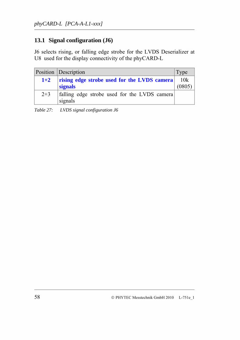
J6 J6 selects rising, or falling edge strobe for the LVDS Deserializer at U8 used for the display connectivity of the phyCARD-L
10k (0805)
1+2 rising edge strobe used for the LVDS camera signals
2+3 falling edge strobe used for the LVDS camera signals
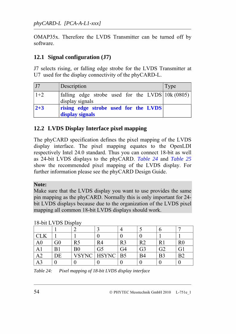
J7 J7 selects rising, or falling edge strobe for the LVDS Transmitter at U7 used for the display connectivity of the phyCARD-L.
10k (0805)
1+2 falling edge strobe used for the LVDS display signals
2+3 rising edge strobe used for the LVDS display signals
0
J10 J10 connects the reset input of the Fast Ethernet Controller (U12) with GPIO_64. Thereby it is possible to perform a reset of the Ehernet Controller, not only by hardware, but also by software.
0R (0805)
open Software reset of the Ethernet Controller disabled
closed Software reset of the Ethernet Controller possible via GPIO_64
J11 J11 allows to connect GPIO_149 to the GPIO1/IRQ1 pin of the X-Arc bus (X2B47) instead of GPIO_145.
0R (0402)
1+2 GPIO1/IRQ1 connects to GPIO_149
2+3 GPIO1/IRQ1 connects to GPIO_145
10
J12 J12 allows to connect GPIO_151 to the GPIO0/IRQ0 pin of the X-Arc bus (X2A46) instead of GPIO_144.
0R (0402)
1+2 GPIO0/IRQ0 connects to GPIO_151
2+3 GPIO0/IRQ0 connects to GPIO_144
10
J13 J13 allows to connect GPIO_146 to the GPIO2/IRQ2/PWM pin of the X-Arc bus (X2A47) instead of GPIO_147.
The phyCARD-L operates off of a single power supply voltage. The following sections of this chapter discuss the primary power pins on the phyCARD-Connector X2 in detail.
4.1 Primary System Power (VDD_3V3)
The phyCARD-L operates off of a primary voltage supply with a nominal value of +3.3V. On-board switching regulators generate the 1.15V, 1.2V and 1.8V voltage supplies required by the OMAP35x MCU and on-board components from the primary 3.3V supplied to the SBC. For proper operation the phyCARD-L must be supplied with a voltage source of 3.3V ±5 % with 1.5 A load at the VCC pins on the phyCARD-Connector X2. VDD_3V3: X2 1A, 2A, 3A, 1B, 2B, 3B Connect all +3.3V VCC input pins to your power supply and at least the matching number of GND pins. Corresponding GND: X2 4A, 8A, 13A, 4B, 8B, 13B Please refer to section 2 for information on additional GND Pins located at the phyCARD-Connector X2. Caution: As a general design rule we recommend connecting all GND pins neighboring signals which are being used in the application circuitry. For maximum EMI performance all GND pins should be connected to a solid ground plane.
For applications requiring a standby mode a secondary voltage source of 3.3V can be attached to the phyCARD-L at pin X2B6. This voltage source is supplying the core and on-chip peripherals of the OMAP35x (e.g. on-chip memory, multimedia accelerator, USB controller, etc.), as well as the PoP memory devices (SDRAM, NAND Flash) while the primary system power (VDD_3V3) is removed. Applications not requiring a standby mode can connect the VSTBY pin to the primary system power supply (VCC = 3.3V), or can leave it open.
4.3 On-board Voltage Regulator (U1)
The phyCARD-L provides an on-board switching regulator (U1) to source the four different voltages (1.15V, 1.2V and 1.8V) required by the processor and on-board components. Figure 8 presents a graphical depiction of the powering scheme. The switching regulator has a single input voltage rail VDD_BKUP as can be seen in Figure 8. VDD_BKUP is supplied from the primary voltage input pins (VDD_3V3) and the secondary voltage input pin VSTBY. Not all devices on the phyCARD-L are supplied from the switching regulator. Some, such as the Ethernet Controller, the LVDS Transmitter, etc. are directly connected to the primary voltage input pins VDD_3V3. The following list summarizes the relation between the different voltage rails and the devices on the phyCARD-L: External voltages: VDD_3V3 and VSTBY (optional) • VDD_3V3: Ethernet Controller, LVDS
Transmitter, LVDS Deserializer • VDD_3V3
or VSTBY � VDD_BKUP: Voltage Regulator
Power Requirements
Internally generated voltages: 1V15, 1V2, 1V8
• 1V15 OMAP35x Core Power Supply.
• 1V2 OMAP35x MPU&IVA Power Supplies.
• 1V8 OMAP35x PLL Power Supply.
• 1V8 OMAP35x MMC Power Supply.
• 1V8 OMAP35x, 32kHz and 26MHz oscillators, EEPROM, USB Transceivers, Ethernet controller, Display LVDS Transmitter.
The voltage level of the phyCARDs logic circuitry is VDD_IO (1.8V) which is generated on-board. In order to allow connecting external devices to the phyCARD-L without the need of another voltage source in addition to the primary supply this voltage is brought out at pins X2A5 and X2B5 of the phyCARD-Connector. Use of level shifters supplied with VDD_IO allows converting the signals according to the needs on the custom target hardware. Alternatively signals can be connected to an open drain circuitry with a pull-up resistor attached to VDD_IO.
The phyCARD-L was designed to support applications requiring a power management. Three pins of the X-Arc bus are designated for this purpose. X_nPWR_OFF and X_nSUSP_RAM are output pins which can be used to indicate the power status of the phyCARD-L, whereas X_nWKUP is an input pin to apply a wake up signal to the phyCARD-L. All three pins lead to GPIOs of the OMAP35x. Thus their functionality can be programmed to your needs. The following table shows the location of the power management pins on the phyCARD-Connector and the corresponding GPIOs of the OMAP35x. Pin # Signal I/O SL Description X2A48 X_nWKUP I VDD_IO Wakeup Interrupt Input
(µC port GPIO_146) X2B26 X_nSUSP_RAM OC VDD_IO Suspend to RAM Open
Collector Output (µC port GPIO_134)
X2B29 X_nPWR_OFF OC VDD_IO Power Off Open Collector Output (µC port GPIO_133)
Table 5: Power Management Pins
With the two output signals X_nPWR_OFF (pin X2B29) and X_nSUSP_RAM (pin X2B26) three different power states can be defined.
X_nSUSP_RAM High Low X X_nPWR_OFF High High Low VDD_3V3 On Off Off VSTBY X On Off
X=don’t care
Table 6: Power States
Please refer to the chapter "Power Management" in the phyCARD Design-In Guide for more information about the implementation of the power management into your design. Caution: According to the specification for the phyCARD family writing custom software to utilize pins X_nSUSP_RAM and X_nPWR_OFF requires them to be configured as Open Collector Output. Use of the power management features of the PMIC at U1 allows for a higher granularity in control of the power consumption. To implement power management with the PMIC it can be programmed via an I2C interface. The TPS65023 can be accessed at I2C address 0x90 / 0x91 (write/read). Please refer to the TPS65023 User's Guide for more information.
Although most features of the OMAP35x microcontroller are configured and/or programmed during the initialization routine, other features, which impact program execution, must be configured prior to initialization via pin termination. The system start-up configuration includes:
• Clock/PLL configuration • Boot device select and boot sequence configuration During the reset cycle the operational system boot mode of the OMAP35x processor is determined by the configuration of the seven external input pins, SYS_BOOT[6:0]. Six external pins (SYS_BOOT[5:0]) are used to select interfaces or devices for booting. Where SYS_BOOT[5] switches between memory (0) and peripheral (1) booting and SYS_BOOT[4:0] define the booting sequence of the interfaces or devices. The settings of these pins control where the system is boot from. They are accessible via boot pins X_CONFIG[1:0] (X2B50 and X2A50) of the phyCARD-L. The boot mode input X_CONFIG0 (X2A50) is connected to SYS_BOOT[5] and allows to choose memory or peripheral boot. If left open SYS_BOOT[5] is low. If X_CONFIG0 is connected to high or low level SYS_BOOT[5] is the inverse of the input level. The boot mode input X_CONFIG1 (X2B50) is attached to SYS_BOOT[4:0]. It is provided for future features and must not be used. It should be left open. A resistor array on the phyCARD-L is used to preconfigure SYS_BOOT[4:0]. The SYS_BOOT[6] pin is used to select whether the internal oscillator is bypassed. It is fixed to high (oscillator bypassed) in the phyCARD-L.
The following table shows the different boot modes applicable for the phyCARD-L. Boot Mode Select. SYS_BOOT[5] ≙ ⌐X_CONFIG01
Boot Mode Select.SYS_BOOT[4:0] ≙X_CONFIG12
Boot Mode/Device
0: X_CONFIG0 = 1, or open
01111 Memory Boot : NAND/USB/UART3/MMC1
1: X_CONFIG0 = 0 01111 Peripheral Boot:
USB/UART3/MMC1/NAND Table 7: Boot Modes of OMAP35x module
The standard phyCARD-L module with 256MB NAND Flash comes with a boot configuration of ‘001111’, so the system will boot from the NAND Flash.
1 : Due to a circuitry on the phyCARD-L SYS_BOOT[5] is low if X_CONFIG0 is left open. 2 : X_CONFIG1 must not be used and should be left open. It is provided for future features. A
resistor array on the phyCARD-L is used to preconfigure SYS_BOOT[4:0]. Customer specific assembly allows to choose other boot modes. Please contact our sales team.
The phyCARD-L provides three types of on-board memory:
• PoP memory device: 256 MByte NAND Flash1 and 256 MByte LP DDR SDRAM
• NAND Flash (VFBGA): 64 MByte (up to 1 GByte) (as an alternative)
• I²C-EEPROM: 4 KB (up to 32 KByte) The following sections of this chapter detail each memory type used on the phyCARD-L.
7.1 LP-DDR-SDRAM and NAND Flash
The system memory of the phyCARD-L is comprised of SDRAM and NAND Flash in a PoP (Package On Package) MCP (Multi Chip Package) or a combination of SDRAM in a POP package and NAND Flash in a VFBGA package. The PoP memory devices are connected to the special SDRC and GPMC interfaces of the OMAP35x processor, configured for 32-bit access, and operating at the maximum frequency of 200MHz. The SDRAM (LPDDR) memory is accessed via the SDRAM controller (SDRC) of the OMAP35x. Typically the LP-DDR-SDRAM initialization is performed by a boot loader or operating system following a power-on reset and must not be changed at a later point by any application code. When writing custom code independent of an operating system or boot loader, SDRAM must be initialized by accessing the appropriate SDRAM configuration registers on the OMAP35x controller. Refer to the OMAP35x Reference Manual for accessing and configuring these registers.
1: Please contact PHYTEC for more information about additional module configurations.
As well the NAND Flash memory in the PoP package as the discrete NAND Flash at U20 are connected to the GPMC bus. This chip select signal is used for boot operation. The discrete NAND Flash is an alternative to the PoP NAND Flash. It can not be added as extension memory. Use of Flash as non-volatile memory on the phyCARD-L provides an easily reprogrammable means of code storage. The following Flash devices can be used on the phyCARD-L: Manufacturer NAND Flash P/N Density
Table 8: Compatible NAND Flash devices Additionally, any POP memory parts that are footprint and functionally compatible with the devices listed above may also be used with the phyCARD-L. These Flash devices are programmable with 1.8 V. No dedicated programming voltage is required. As of the printing of this manual these NAND Flash devices generally have a life expectancy of at least 100,000 erase/program cycles and a data retention rate of 10 years.
7.2 I²C EEPROM (U10)
The phyCARD-L is populated with a ST 24W32C1 non-volatile 4 KByte EEPROM with an I²C interface at U10. This memory can be used to store configuration data or other general purpose data. This device is accessed through I²C port 2 on the OMAP35x. The control registers for I²C port 2 are mapped between addresses 0x4807 2004 and 0x4807 2054. Please see the OMAP35x Reference Manual for detailed information on the registers.
1: See the manufacturer’s data sheet for interfacing and operation.
Three solder jumpers are provided to set the lower address bits: J1, J2 and J3. Refer to section 7.2.1 for details on setting these jumpers. Write protection to the device is accomplished via jumper J5. Refer to section 7.2.2 for further details on setting this jumper.
7.2.1 Setting the EEPROM Lower Address Bits (J3, J2, J1)
The 4 KB I²C EEPROM populating U10 on the phyCARD-L module has the capability of configuring the lower address bits A0, A1, and A2. The four upper address bits of the device are fixed at ‘1010’ (see ST 24W32C data sheet). The remaining three lower address bits of the seven bit I²C device address are configurable using jumpers J1, J2 and J3. J3 sets address bit A0, J2 address bit A1, and J1 address bit A2. Table 9 below shows the resulting seven bit I²C device address for the eight possible jumper configurations.
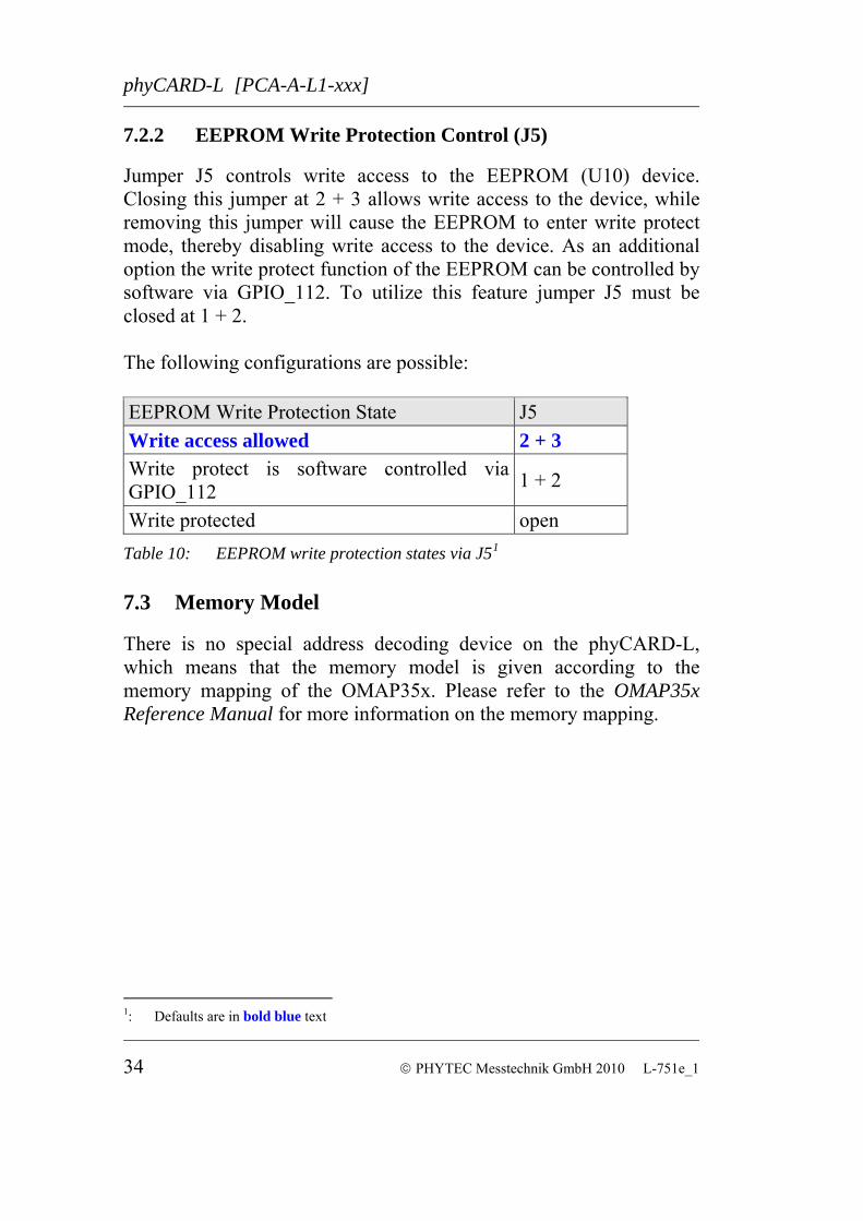
Jumper J5 controls write access to the EEPROM (U10) device. Closing this jumper at 2 + 3 allows write access to the device, while removing this jumper will cause the EEPROM to enter write protect mode, thereby disabling write access to the device. As an additional option the write protect function of the EEPROM can be controlled by software via GPIO_112. To utilize this feature jumper J5 must be closed at 1 + 2. The following configurations are possible: EEPROM Write Protection State J5 Write access allowed 2 + 3 Write protect is software controlled via GPIO_112 1 + 2
Write protected open Table 10: EEPROM write protection states via J51
7.3 Memory Model
There is no special address decoding device on the phyCARD-L, which means that the memory model is given according to the memory mapping of the OMAP35x. Please refer to the OMAP35x Reference Manual for more information on the memory mapping.
The X-Arc bus features an SD / MMC Card interface. On the phyCARD-L the interface signals extend from the controllers first Multimedia Card / Secure Digital / Secure Digital I/O (MMC/SD/SDIO) Host Controller (MMC1) to the phyCARD-Connector. Table 11 shows the location of the different interface signals on the phyCARD-Connector. The MMC/SD/SDIO Host Controller is fully compatible with the SD Memory Card Specification 2.0 and SD I/O Specification 1.1 with 1 and 4 channel(s) (refer to the OMAP35x Reference Manual for more information). Due to compatibility reasons a card detect signal (X_SDIO_CD) is added to the SD / MMC Card Interface. This signal connects to port GPIO_126 of the OMAP35x. Pin # Signal I/O SL Description
X2A31 X_SDIO_D0 I/O VDD_IO SD/MMC Data line both in 1-bit and 4-bit mode
X2A32 X_SDIO_D2 I/O VDD_IO SD/MMC Data line both in 1-bit and 4-bit mode
X2A33 X_SDIO_CLK O VDD_IO SD/MMC Clock for MMC/SD/SDIO
X2B31 X_SDIO_D1 I/O VDD_IO SD/MMC Data line both in 1-bit and 4-bit mode
X2B32 X_SDIO_D3 I/O VDD_IO SD/MMC Data line both in 1-bit and 4-bit mode
X2B33 X_SDIO_CMD O VDD_IO SD/MMC Command for MMC/SD/SDIO
X2B46 X_SDIO_CD I VDD_IO SD/MMC Card Detect for MMC/SD/SDIO
Table 11: Location of SD/ MMC Card interface signals
Note: The signal level of the SD / MMC card interface is 1.8V. Thus integration of an SD / MMC card slot on custom target hardware requires level shifters supplied with VDD_IO (X2A5 and X2B5) at one of the supply rails. Please refer to the chapter "SD / MMC" in the phyCARD Design-In Guide for more information about connecting an SD / MMC Card slot to the phyCARD-L.
The phyCARD-L provides seven serial interfaces some of which are equipped with a transceiver to allow direct connection to external devices: 1. High speed UART (TTL, derived from UART3 of the
OMAP35x) with up to 3.6 Mbit/s and hardware flow control (RTS and CTS signals)
2. High speed USB OTG interface consisting of the OMAP35x USB OTG interface and an additional USB transceiver
3. High speed USB HOST interface based on the OMAP35x USB Host interface and an additional USB transceiver
4. Auto-MDIX enabled 10/100 Ethernet interface implemented with an Ethernet controller attached to the OMAP35x GPMC interface
5. I2C interface (derived from third I2C port of the OMAP35x) 6. Serial Peripheral Interface (SPI) interface (extended from the first
SPI module of the OMAP35x) 7. Synchronous Serial Interface (SSI) with AC'97 support
(originating from the synchronous serial interface (McBSP) of the OMAP35x)1
The following sections of this chapter detail each of these serial interfaces and any applicable configuration jumpers. Caution: Please pay special attention to the Signal Level (SL) column in the following tables. Some of the serial interfaces signal level is VDD_IO, which is 1.8V and which is not identical with the voltage level of the primary supply voltage of the phyCARD-L. When connecting these interfaces to external devices level shifters supplied with VDD_IO (X2A5 and X2B5) at one of the supply rails should be used.
1: Since the OMAP35x does not support AC'97 protocol, the AC'97 interface on the
phyCARD-L is software emulated. The emulation is part of the BSP delivered with the phyCARD-L.
Please refer to the phyCARD Design-In Guide (LAN-051) for more information about using the serial interfaces of the phyCARD-L in customer applications.
9.1 Universal Asynchronous Interface
The phyCARD-L provides a high speed universal asynchronous interface with up to 3.6 Mbit/s and hardware flow control (RTS and CTS signals). The following table shows the location of the signals on the phyCARD-Connector. Pin # Signal I/O SL Description
X2A39 X_UART_TXD O VDD_IO Serial transmit signal UART 3
X2A40 X_UART_RTS O VDD_IO Request to send UART 3
X2B39 X_UART_RXD I VDD_IO Serial data receive signal UART 3
X2B40 X_UART_CTS I VDD_IO Clear to send UART 3 Table 12: Location of the UART signals The signals extend from UART3 of the OMAP35x directly to the phyCARD-Connector without conversion to RS-232 level. External RS-232 transceivers must be attached by the user if RS-232 levels are required.
The phyCARD-L is populated with an NXP ISP1504 USB On-The-Go High-Speed transceiver at U16 which is capable of high speed, full speed, and low speed data transmission. The ISP1504 functions as the transceiver for the OMAP35x High Speed USB OTG Controller (HSUSB0). An external USB Standard-A (for USB host), USB Standard-B (for USB device), or USB mini-AB (for USB OTG) connector is all that is needed to interface the phyCARD-L USB OTG functionality. The applicable interface signals can be found on the phyCARD-Connector as shown in Table 13. Pin # Signal I/O SL Description
X2A23 X_USBOTG_PWR O VDD_3V3USB-OTG Power switch output open drain
X2A24 X_USBOTG_OC I VDD_3V3 USB-OTG over current input signal
X2A26 X_ USBOTG_VBUS I 5V USB VBUS Voltage
X2A27 X_USBOTG_DM I/O USB transceiver cable interface, D-
X2A28 X_USBOTG_DP I/O USB transceiver cable interface, D+
X2A29 X_USBOTG_UID I USB on the go transceiver cable ID resistor connection
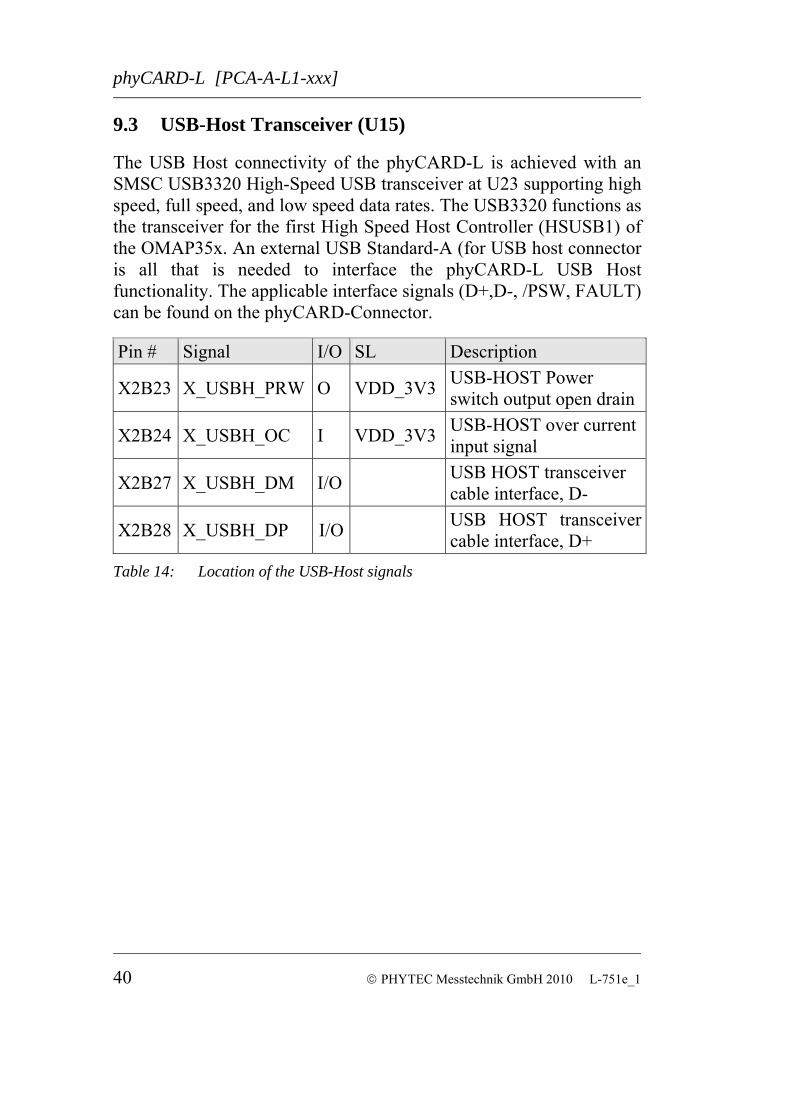
The USB Host connectivity of the phyCARD-L is achieved with an SMSC USB3320 High-Speed USB transceiver at U23 supporting high speed, full speed, and low speed data rates. The USB3320 functions as the transceiver for the first High Speed Host Controller (HSUSB1) of the OMAP35x. An external USB Standard-A (for USB host connector is all that is needed to interface the phyCARD-L USB Host functionality. The applicable interface signals (D+,D-, /PSW, FAULT) can be found on the phyCARD-Connector.
Pin # Signal I/O SL Description
X2B23 X_USBH_PRW O VDD_3V3 USB-HOST Power switch output open drain
X2B24 X_USBH_OC I VDD_3V3 USB-HOST over current input signal
X2B27 X_USBH_DM I/O USB HOST transceiver cable interface, D-
X2B28 X_USBH_DP I/O USB HOST transceiver cable interface, D+
Connection of the phyCARD-L to the world wide web or a local area network (LAN) is possible using the on-board FEC (Fast Ethernet Controller) at U12. It is connected to the GPMC interface of the OMAP35x. The FEC operates with a data transmission speed of 10 or 100 Mbit/s.
9.4.1 Ethernet Controller (U12)
With an Ethernet controller mounted at U12 the phyCARD-L has been designed for use in 10Base-T and 100Base-T networks. The 10/100Base-T interface with its LED signals extends to phyCARD-Connector X2.
Pin # Signal I/O SL Description
X2A19 X_ETH_SPEED O VDD_3V3 Ethernet Speed Indicator (Open Drain)
The Ethernet controller's integrated PHY supports HP Auto-MDIX technology, eliminating the need for the consideration of a direct connect LAN cable, or a cross-over patch cable. It detects the TX and RX pins of the connected device and automatically configures the PHY TX and RX pins accordingly. The Ethernet controller also features an Auto-negociation to automatically determine the best speed and duplex mode. The Ethernet controller is connected to chip select CS5 of the General-Purpose Memory Controller (GPMC). Please refer to the OMAP35x Reference Manual for more information on how to configure the address space for CS5 etc. In order to connect the module to an existing 10/100Base-T network some external circuitry is required. The required 49,9 Ohm +/-1% termination resistors on the analog signals (ETH_RX±, ETH_TX±) are already populated on the module. Connection to an external Ethernet magnetics should be done using very short signal traces. The TPI+/TPI- and TPO+/TPO- signals should be routed as 100 Ohm differential pairs. The same applies for the signal lines after the transformer circuit. The carrier board layout should avoid any other signal lines crossing the Ethernet signals. An example for the external circuitry is shown in the phyCARD's Design Guide. If you are using the applicable Carrier Board for the phyCARD-L (part number PBA-A-01), the external circuitry mentioned above is already integrated on the board (refer to section 17.3.4). Caution! Please see the datasheet of the Ethernet controller as well as the phyCARD's Design Guide (LAN-051) when designing the Ethernet transformer circuitry.
9.4.2 Software Reset of the Ethernet Controller (J10)
The Ethernet controller at U12 can be reset either by hardware, or software reset. The reset input of the Ethernet controller is permanently connected to the global reset signal of the phyCARD-L, which can be performed by either the on-board switching regulator at U1 or via pin X2A7 of the phyCARD-Connector. Jumper J10 connects the reset input of the Ethernet controller with GPIO_64. This allows to also reset the Ethernet controller by software. J10 is not mounted. To enable a software reset of the Ethernet controller J10 must be closed. The following configurations are possible:
Software reset of the Ethernet controller J10 Software reset disabled open Software reset possibel via GPIO_64 closed
Table 16: Software Reset of the Ethernet Controller 1
9.4.3 MAC Address
In a computer network such as a local area network (LAN), the MAC (Media Access Control) address is a unique computer hardware number. For a connection to the Internet, a table is used to convert the assigned IP number to the hardware's MAC address. In order to guarantee that the MAC address is unique, all addresses are managed in a central location. PHYTEC has acquired a pool of MAC addresses. The MAC address of the phyCARD-L is located on the bar code sticker attached to the module. This number is a 12-digit HEX value. An EEPROM at U13 is used to store the MAC address.
The Inter-Integrated Circuit (I2C) interface is a two-wire, bidirectional serial bus that provides a simple and efficient method for data exchange among devices. The OMAP35x contains three identical and independent multimaster high-speed I2C modules. The interface of the third module is available on the phyCARD-Connector. Whereas the first module connects the on-board PMIC (U1) (refer to section 4.3) and the second module connects to the on-board EEPROM (refer to section 7.2). The following table lists the I2C port on the phyCARD-Connector:
Pin # Signal I/O SL Description X2A17 X_I2C_SCL O VDD_IO I2C Clock Output X2B17 X_I2C_SDA I/O VDD_IO I2C Data
Table 17: I2C Interface Signal Location
9.6 SPI Interface
The Serial Peripheral Interface (SPI) interface is a four-wire, bidirectional serial bus that provides a simple and efficient method for data exchange among devices. 6 pins of the X-Arc bus are designated to the SPI interface (refer to Table 2). In addition to the four standard signals a second chip select and the SPI ready signal are provided at the X-Arc bus. The later signal allows to also use SPI devices with "5-wire protocol". The OMAP35x contains four SPI modules. The interface signals of the first module (McSPI1) are made available on the phyCARD-Connector. This module is Master/Slave configurable. The OMAP35x does not provide the SPI ready signal. Because of that a third chip select signal (McSPI1_CS2) is attached to pin X2A36 instead. The following table lists the SPI signals on the phyCARD-Connector:
Pin # Signal I/O SL Description X2A35 X_SPI_CS0 O VDD_IO McSPI1 Chip select 0 X2B35 X_SPI_CS1 O VDD_IO McSPI1 Chip select 1 X2A36 X_SPI_RDY O VDD_IO McSPI1 Chip select 2 X2A37 X_SPI_CLK O VDD_IO McSPI1 clock X2B36 X_SPI_MOSI I/O VDD_IO McSPI1 Master data out;
slave data in X2B37 X_SPI_MISO I/O VDD_IO McSPI1 Master data in;
slave data out Table 18: SPI Interface Signal Location
9.7 Synchronous Serial Interface (SSI)
The multi-channel buffered Serial Port (McBSP) interface of the phyCARD-L is a full-duplex, serial interface that allows to communicate with a variety of serial devices, such as standard codecs, digital signal processors (DSPs), microprocessors, peripherals, and popular industry audio codecs that implement the inter-IC sound bus standard (I2S) and Intel AC'97 standard. The OMPA35x provides five instances of the MCBSP module. On the phyCARD-L McBSP2 is brought out to the phyCARD-Connector. With reference to the X-Arc bus specification, the main purpose of this interface is to connect to an external codec, such as AC'971. Four signals extend from the OMAP35x McBSP module to the phyCARD-Connector (X_AC97/HDA_SDOUT, X_AC97/HDA_SDIN, X_AC97/HDA_BITCLK, X_AC97/HDA_SYNC). X_AC97/HDA_INT/SEL and X_AC97/HDA_nRST are two additional pins assisting the functionality of this interface. X_AC97/HDA_INT/SEL is used as input and output. As output it signals which codec is supported by the phyCARD. Use of this pin as an input enables to attach an external interrupt to GPIO_160.
1: Since the OMAP35x does not support AC97 protocol, the AC97 interface on the
phyCARD-L is software emulated. The emulation is spart of the BSP delivered with the phyCARD-L.
X_AC97/HDA_nRST is connected to GPIO_156 of the OMAP35x allowing to perform a software reset for the device attached to the interface. Please also read the phyCARD Design-In Guide for more information about how to use the AC'97 interface. Pin # Signal I/O SL Description X2A42 X_AC97/HDA_INT/SEL I/O VDD_IO AC'97 Interrupt Input X2A43 X_AC97/HDA_SDOUT O VDD_IO AC'97 Transmit
Output X2A44 X_AC97/HDA_SDIN I VDD_IO AC'97 Receive Input X2B42 X_AC97/HDA_BITCLK I VDD_IO AC'97 Clock X2B43 X_AC97/HDA_SYNC O VDD_IO AC'97 SYNC X2B44 X_AC97/HDA_nRST O VDD_IO AC'97 Reset
The X-Arc bus provides 3 GPIO / IRQ signals. Table 20 shows the location of the GPIO / IRQ pins on the phyCARD-Connector, as well as the corresponding ports of the OMAP35x. Pin # Signal I/O SL Description
X2A46 X_GPIO0/IRQ0 I/O VDD_IO GPIO0_IRQ0 connected to µC GPIO_144 or GPIO_1511
X2A47 X_GPIO2/IRQ2/PWM I/O VDD_IO GPIO2_IRQ2 connected to µC GPIO_147 or GPIO_1461
X2B47 X_GPIO1/IRQ1 I/O VDD_IO GPIO1_IRQ1 connected to µC GPIO_145 or GPIO_1491
Table 20: Location of GPIO and IRQ pins
As can be seen in the table above the voltage level is VDD_IO, which is 1.8 V. In other words VDD_IO is not identical with the supply voltage of the phyCARD-L. To avoid mismatch of the different voltage levels external devices connected to these pins should be supplied by VDD_IO available at X2A5 and X2B5 (refer to section 4.4). Alternatively an open drain circuit with a pull-up resistor attached to VDD_IO can be connected to the GPIOs of the phyCARD-L. Please refer to the chapter "GPIOs" in the phyCARD Design-In Guide for more information about how to integrate the GPIO pins in your design.
1 : can be selected by jumper (refer to section 3)
Three jumpers (J11, J12 and J13) allow to choose different GPIOs of the OMAP35x to be connected to the GPIO_IRQ pins of the X-Arc bus. The following table shows the possible configurations. Jumper Description Type J11 J11 allows to connect GPIO_149 to the
GPIO1/IRQ1 pin of the X-Arc bus (X2B47) instead of GPIO_145.
0R (0402)
1+2 GPIO1/IRQ1 connects to GPIO_149 2+3 GPIO1/IRQ1 connects to GPIO_145
J12 J12 allows to connect GPIO_151 to the GPIO0/IRQ0 pin of the X-Arc bus (X2A46) instead of GPIO_144.
0R (0402)
1+2 GPIO0/IRQ0 connects to GPIO_151 2+3 GPIO0/IRQ0 connects to GPIO_144
J13 J13 allows to connect GPIO_146 to the GPIO2/IRQ2/PWM pin of the X-Arc bus (X2A47) instead of GPIO_147.
0R (0402)
1+2 GPIO2/IRQ2/PWM connects to GPIO_146 2+3 GPIO2/IRQ2/PWM connects to GPIO_147
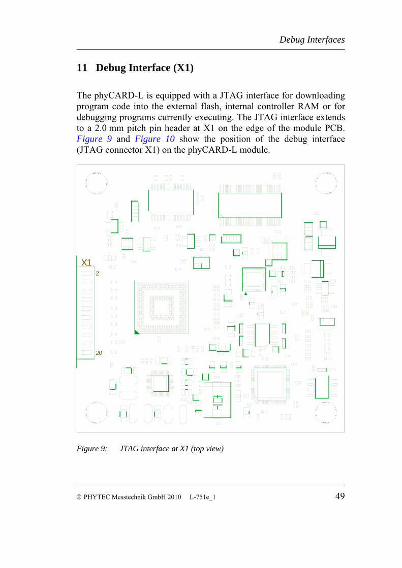
The phyCARD-L is equipped with a JTAG interface for downloading program code into the external flash, internal controller RAM or for debugging programs currently executing. The JTAG interface extends to a 2.0 mm pitch pin header at X1 on the edge of the module PCB. Figure 9 and Figure 10 show the position of the debug interface (JTAG connector X1) on the phyCARD-L module.
pulldown) Table 22: JTAG connector X1 signal assignment
*Note: Row A is on the controller side of the module and row B is on the connector side of the module PHYTEC offers a JTAG-Emulator adapter (order code JA-002) for connecting the phyCARD-L to a standard emulator. The JTAG-Emulator adapter extends the signals of the module's JTAG connector to a standard ARM connector with 2 mm pin pitch. The JA-002 therefore functions as an adapter for connecting the module's non-ARM-compatible JTAG connector X1 to standard Emulator connectors.
The phyCARD-L uses a SN65LVDS83B 4-Channel 24-Bit LVDS Transmitter (U7) to generate LVDS-Signals from the parallel TTL Display Interface. Thus you can connect a LVDS-Display to the phyCARD-L. The location of the applicable interface signals (X_DIS_LVDS_TX0-3+, X_DIS_LVDS_TX0-3-, X_DIS_LVDS_TXCLK+ and X_DIS_LVDS_TXCLK-) can be found in the table below.
Pin # Signal I/O SL Description
X2A9 X_DIS_LVDS_TX0+ O LVDS LVDS chanel 0 pos. output
X2A10 X_DIS_LVDS_TX0- O LVDS LVDS chanel 0 neg. output
X2A11 X_DIS_LVDS_TX2+ O LVDS LVDS chanel 2 pos. output
X2A12 X_DIS_LVDS_TX2- O LVDS LVDS chanel 2 neg. output
X2A14 X_DIS_LVDS_TXCLK+ O LVDS LVDS Clock pos. output
X2A15 X_DIS_LVDS_TXCLK- O LVDS LVDS Clock neg. output
X2B9 X_DIS_LVDS_TX1+ O LVDS LVDS chanel 1 pos. output
X2B10 X_DIS_LVDS_TX1- O LVDS LVDS chanel 1 neg. output
X2B11 X_DIS_LVDS_TX3+ O LVDS LVDS chanel 3 pos. output
X2B12 X_DIS_LVDS_TX3- O LVDS LVDS chanel 3 neg. output
Table 23: Display Interface Signal Location To assists the implementation of a power managment the LVDS Transmitter's SHTDN input is connected to GPIO_26 of the
phyCARD-L [PCA-A-L1-xxx]
OMAP35x. Therefore the LVDS Transmitter can be turned off by software.
12.1 Signal configuration (J7)
J7 selects rising, or falling edge strobe for the LVDS Transmitter at U7 used for the display connectivity of the phyCARD-L. J7 Description Type 1+2 falling edge strobe used for the LVDS
display signals 10k (0805)
2+3 rising edge strobe used for the LVDS display signals
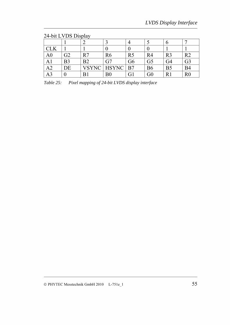
12.2 LVDS Display Interface pixel mapping
The phyCARD specification defines the pixel mapping of the LVDS display interface. The pixel mapping equates to the OpenLDI respectively Intel 24.0 standard. Thus you can connect 18-bit as well as 24-bit LVDS displays to the phyCARD. Table 24 and Table 25 show the recommended pixel mapping of the LVDS display. For further information please see the phyCARD Design Guide. Note: Make sure that the LVDS display you want to use provides the same pin mapping as the phyCARD. Normally this is only important for 24-bit LVDS displays because due to the organization of the LVDS pixel mapping all common 18-bit LVDS displays should work. 18-bit LVDS Display 1 2 3 4 5 6 7 CLK 1 1 0 0 0 1 1 A0 G0 R5 R4 R3 R2 R1 R0 A1 B1 B0 G5 G4 G3 G2 G1 A2 DE VSYNC HSYNC B5 B4 B3 B2 A3 0 0 0 0 0 0 0
Table 24: Pixel mapping of 18-bit LVDS display interface
The phyCARD-L uses a DS92LV1212A 1-channel 10-Bit LVDS Random Lock Deserializer (U8) to receive LVDS-Signals from a LVDS Camera Interface. The LVDS Deserializer converts the LVDS signal to a 10-bit wide parallel data bus and separate clock which can be used as inputs for the OMAP35x Camera Sensor Interface. The 10-bit wide data bus consists of 8 color information bits and 2 sync bits (HSYNC/VSYNC). The following table shows the location of the applicable interface signals (X_CAM_LVDS_MCLK, X_CAM_LVDS_nLOCK, X_CAM_LVDS_RX+, X_CAM_LVDS_RX-) on the phyCARD-Connector. Pin # Signal I/O SL Description
X2A16 X_CAM_LVDS_MCLK O VDD_IO Clock output for Camera Interface
X2B14 X_CAM_LVDS_RX+ O LVDS LVDS Receive positive Input for Camera
X2B15 X_CAM_LVDS_RX- O LVDS LVDS Receive negative Input for Camera
X2B16 X_CAM_LVDS_nLOCK O VDD_IO Lock output for Camera Interface
Table 26: Camera Interface Signal Location To assists the implementation of a power managment the Deserializer's REN input is connected to GPIO_167 of the OMAP35x. Therefore the LVDS Deserializer can be turned off by software.
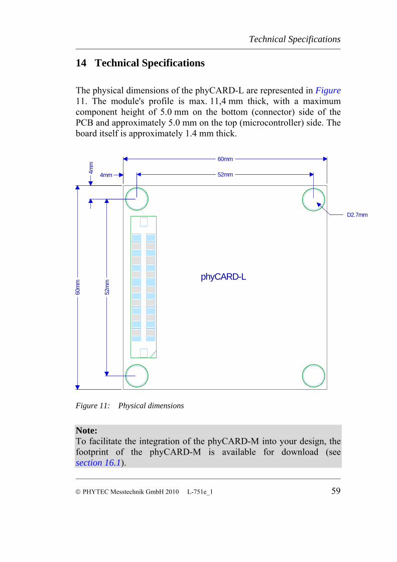
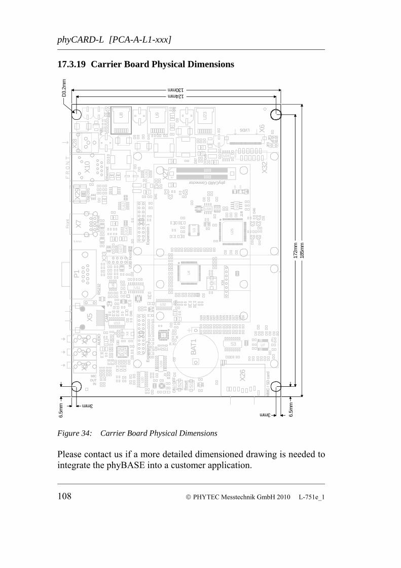
The physical dimensions of the phyCARD-L are represented in Figure 11. The module's profile is max. 11,4 mm thick, with a maximum component height of 5.0 mm on the bottom (connector) side of the PCB and approximately 5.0 mm on the top (microcontroller) side. The board itself is approximately 1.4 mm thick.
D2.7mm
52m
m
4mm
52mm4mm
60mm
60m
m
phyCARD-L
F
Note: To facilitate the integration of the phyCARD-M into your design, the footprint of the phyCARD-M is available for download (see section 16.1).
f pins per contact rows Molex part number (lead free)
are offered le sockets that nectors p
The givedistance between the two conne ule is
the corresponding carr the exact m component h m) on the bottom side
of the phyCORE must be subtracted.
ponent height 6 mm
Manufacturer Number of pins per contact row Molex part number (lead free) ader)
Manufacturer Molex Number of pins per contact row 100 (2 rows of 50 pins each) Molex part number (lead free) 53553-1079 (header) Please refer to the corresponding data sheets and mechanical specifications provided by Molex (www.molex.com).
Connectors on the phyCA Manufacturer Molex Number o 100 (2 rows of 50 pins each)
52885-1074 (receptacle)
Two different heights for the receptaccorrespond to the conphyCARD—OMAP35x.
opulating the underside of the n connector height indicates the cted PCBs when the mod
mounted on ier board. In order to get spacing, the maximu eight (2,5 m
Com
Molex 100 (2 rows of 50 pins each) 55091-1075/1074 (he
16 Hints for Integrating and Handling the phyCARD-L
16.1
1.
2.
3.
4.
5.
Integrating the phyCARD-M
Besides thi hardware manual much information is available to facilitate the integration of the phyCARD-M into customer applications.
the design of the stamdard phyBASE Carrier Board can be used a reference for ny customer application
many answers to common questi ns can be found at http://www.phytec.de/de/support/faq/faq-phycard-m.html, or http://www.phytec.eu/europe/support/faq/faq-phycard-m.html. a Design-In Guide can be downloaded from the same web side. It provides recommendations as to development of customized Car r Bo d target hardware in which the p yCARD-M (and other phyCARDs) can be deployed. the link "Carrier Board" within the category Dimensional Drawing leads to the t d ta as s o n in Figure 14. It is available in different file formats. different support packages are available to support you in all stages of your embedded development. Please visite http://www.phytec.de/de/support/support-pake .h , or http://www.phytec.eu/europe/support/support-packages.html, or contact our sales team for more details.
• Modifications on the phyCARD Module Removal of various components, such as the microcontroller and the standard quartz, is not advisable given the compact nature of the module. Should this nonetheless be necessary, please ensure that the board as well as surrounding components and sockets remain undamaged while de-soldering. Overheating the board can cause the solder pads to loosen, rendering the module inoperable. Carefully heat neighboring connections in pairs. After a few alternations, components can be removed with the solder-iron tip. Alternatively, a hot air gun can be used to heat and loosen the bonds. Caution! If any modifications to the module are performed, regardless of their nature, the manufacturer guarantee is voided. • Integrating the phyCARD into a Target Application Successful integration in user target circuitry greatly depends on the adherence to the layout design rules for the GND connections of the phyCARD module. As a general design rule we recommend connecting all GND pins neighboring signals which are being used in the application circuitry. For maximum EMI performance all GND pins should be connected to a solid ground plane. Note! Please refer to the phyCARD Design-In Guide (LAN-051) for additional information, layout recommendations and example circuitry.
PHYTEC phyBASE Boards are fully equipped with all mechanical and electrical components necessary for the speedy and secure start-up and subsequent communication to and programming of applicable PHYTEC Single Board Computer (SBC) modules. phyBASE Boards are designed for evaluation, testing and prototyping of PHYTEC Single Board Computers in laboratory environments prior to their use in customer designed applications. The phyBASE supports the following features for the phyCARD-L modules: • Power supply circuits to supply the modules and the peripheral
devices • Support of different power modes of appropriate phyCARDs • Full featured 4 line RS-232 transceiver supporting data rates of up
to 120 kbps, hardware handshake and RS-232 connector • Seven USB-Host interfaces • USB-OTG interface • 10/100 Mbps Ethernet interface • Complete audio and touch screen interface • LVDS display interface with separate connectors for data lines and
display / backlight supply voltage • Circuitry to allow dimming of a backlight • LVDS camera interface with I2C for camera control • Secure Digital Card / Multi Media Card Interface • Two expansion connectors for PHYTEC Extension Boards (PEBs)
or customer prototyping purposes featuring one USB, one I2C and one SPI interface, as well as one GPIO/IRQ at either connector
• DIP-Switch to configure various interface options • Jumper to configure the boot options for the phyCARD-L module
The phyBASE Carrier Board provides a flexible development
his modular development platform concept the following
applicable SBC circuitry such as DDR SDRAM, Flash,
ents and uding: a power socket which enables
ternal power adapter, interface connectors et allowing for use of the SBC's
ific information relevant to the the phyBASE Carrier
17.1 Concept of the phyBASE Board
platform enabling quick and easy start-up and subsequent programming of the phyCARD Single Board Computer module. The Carrier Board design allows easy connection of additional expansion boards featuring various functions that support fast and convenient prototyping and software evaluation. The Carrier Board is compatible with all phyCARDs. Tcomponents: • the phyCARD-L module populated with the OMAP35x processor
and all PHYs, and transceivers to name a few.
• the phyBASE which offers all essential compon
connectors for start-up inclconnection to an exsuch as DB-9, USB and Etherninterfaces with standard cable.
The following sections contain specoperation of the phyCARD-L mounted onBoard. Note: Only features of the phyBASE which are supported by the phyCARD-L are described. Jumper settings and configurations which are not suitable for the phyCARD-L are not described in the following chapters.
Figure 15: phyBASE Overview of Connectors, LEDs and Buttons
17.2 Overview of the phyBASE Periph
The phyBASE is depicted in Figure 15. It is equipped with the components and peripherals listed in Table 28, Table 29, Table 30 and Table 31. For a more detailed description of each peripheral refer to the appropriate chapter listed in the applicable table. Figure 15 highlights the location of each peripheral for easy identification.
Table 28 lists all available connectors on the phyBASE. Figure 15 highlights the location of each connector for easy identification. Reference Designator Description See
Section X1 Stereo Microphone input connector 17.3.9 X2 Stereo Line out connector 17.3.9 X3 Stereo Line In connector 17.3.9 X5 Camera Interface, RJ45 17.3.8 X6 Display data connector 17.3.7.1 X7 Dual USB Host connector 17.3.5 X8A Expansion connector 0 17.3.13 X9A Expansion connector 1 17.3.13
X10 Ethernet connector, RJ45 with speed and link led
17.3.4
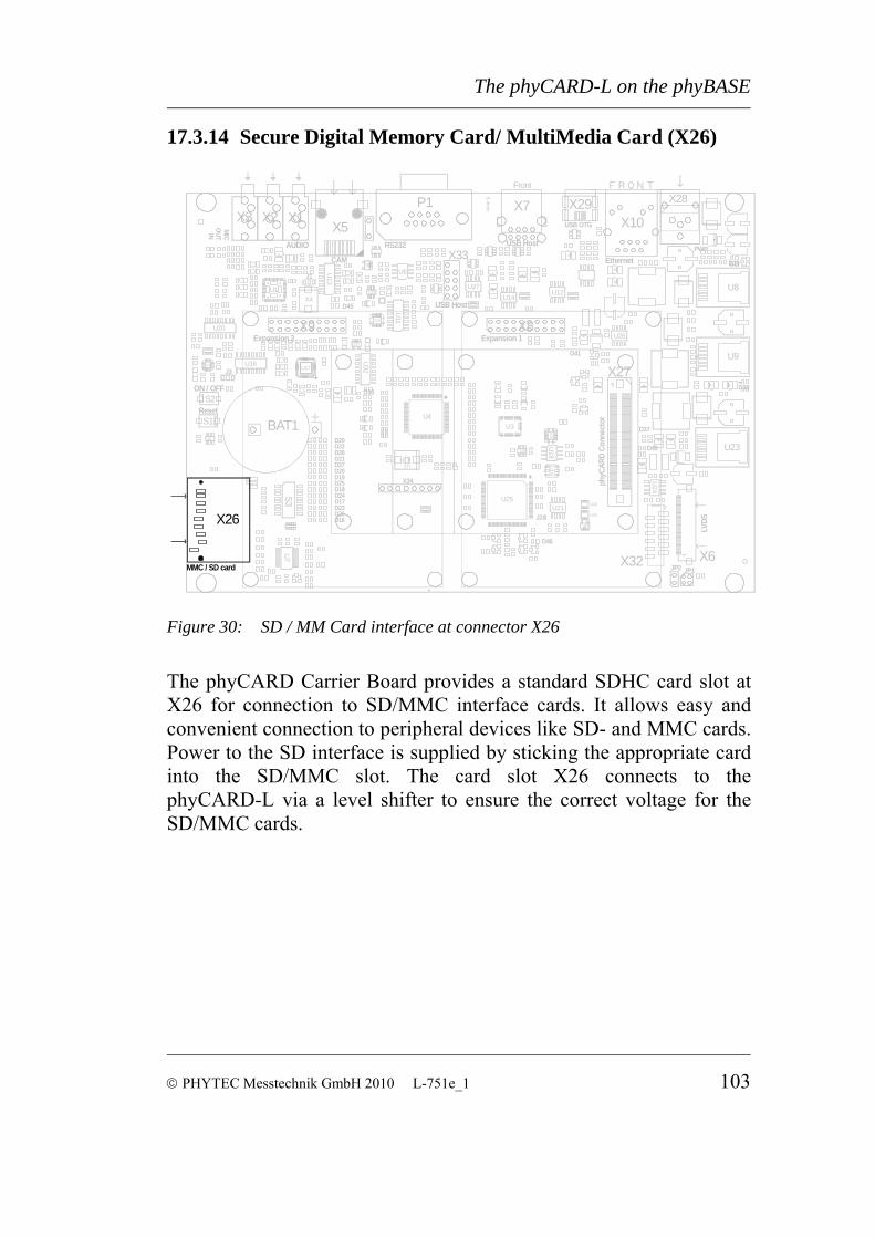
X26 Secure Digital/MultiMedia Card slot 17.3.14
X27 phyCARD-Connector for mounting the phyCARD-L
17.3.1
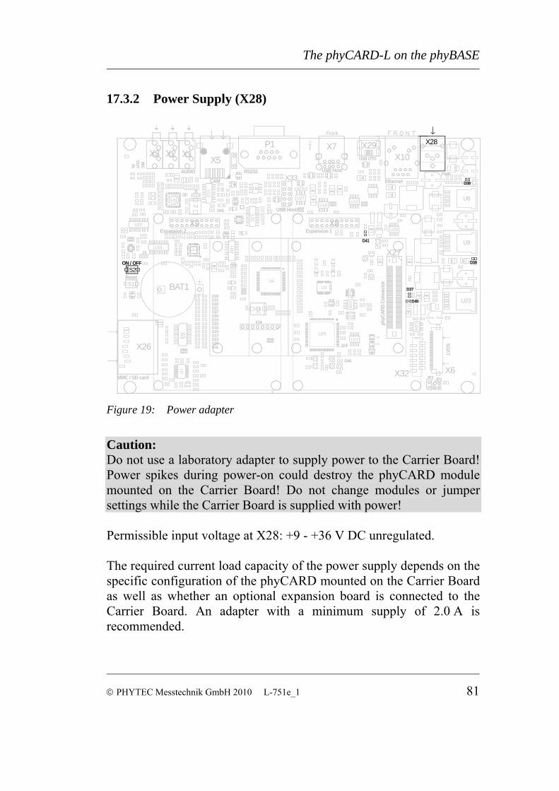
X28 Wall adapter input power jack to supply main board power (+9 - +36 V)
17.3.2
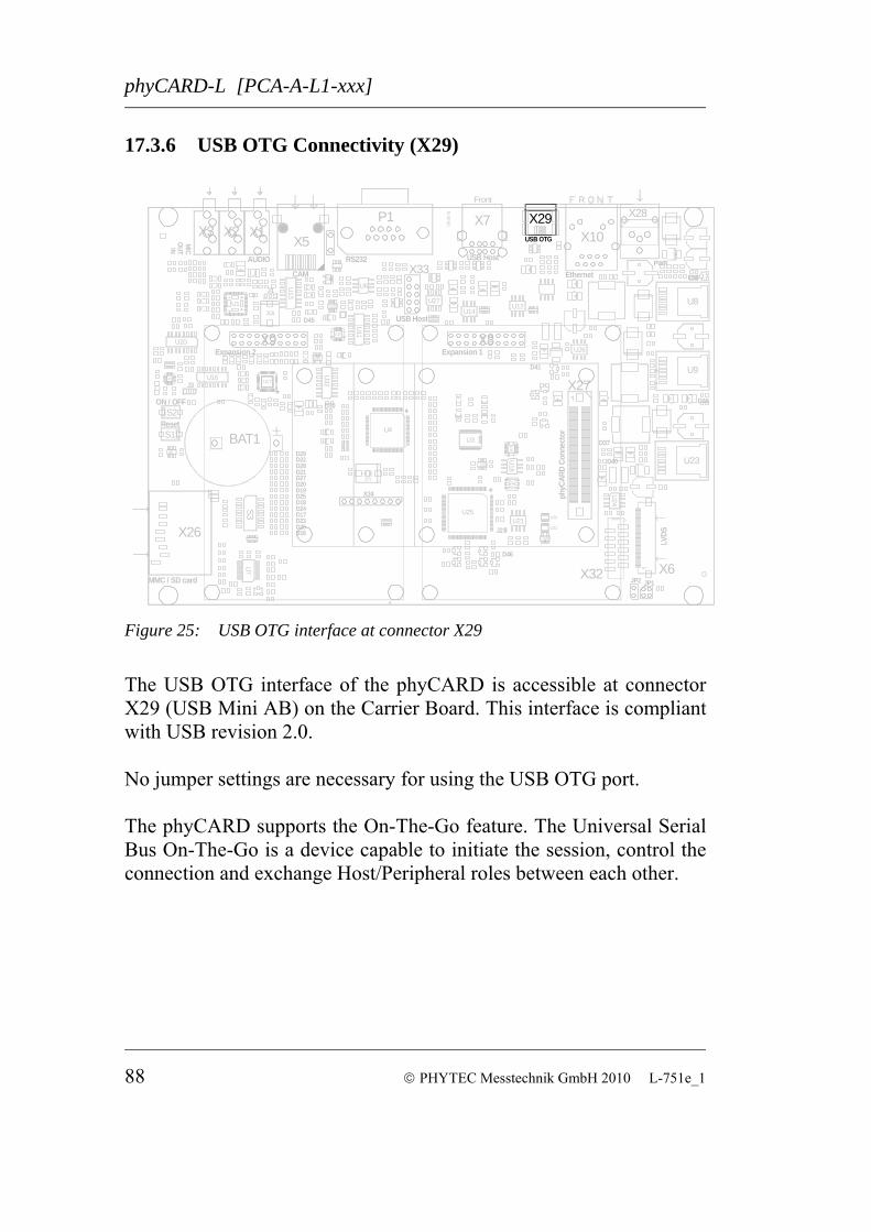
X29 USB On-The-Go connector 17.3.6
X32 Display / Backlight supply voltage connector
17.3.7.2
X33 USB Host connector 17.3.5
X34 CPLD JTAG connector for internal use only
P1 Serial Interface, DB-9F 17.3.3 Table 28: phyBASE Connectors and Pin Headers
The phyCARD-L on the phyBASE
Note: The signal levels of the I C and SPI interface are shifted from 2
VCC_LOGIC (1.8V) at the phyCARD Connector to VCC3V3 (3.3 V) by level shifters on the phyCARD Carrier Board. Ensure that all module connections are not to exceed their expressed m ol ent. Maximum signal input values are aximum v tage or currindicated in the corresponding controller User's Manual/Data Sheets. As damage fro ording to use and m improper connections varies acca cation, it y to take appropr ety ppli is the user‘s responsibilit iate safm ures to e nections are prote m eas nsure that the module con cted froo oading th ls.
17.2.2 Switc
T yBASEt ration o le on the Carrier Boa e 1 s the lo nd push buttons.
verl rough connected periphera
hes
he phhe ope
is populated with some f the phyCARD-L modu
switches which are essential for rd. Figur
5 show cation of the switches a
ButtoSee
n Description Section S1 Sys
gen 17.3tem Reset Button – system reset signal eration .16
S2 Powsupp 17.3er Button – powering on and off main
ly voltages of the Carrier Board .2
Table 29: phy
S1 Issues a system reset signal. Pressing this button will toggle the
RESET the phyCARD microcontroller LOW, causing the controller to reset.
S2 Issues a power on/off event. Pressing this button l
seconds will toggle the PWR_KEY pin of the phyBASE CPLD LOW, causing the CPLD to turn
es the CPLD to turn off the supply voltages.
BASE push buttons descriptions
n _IN pin (X2A7) of
ess than 2
on the supply voltages. Pressing this button for more than 2 seconds caus
nally a DIP-Switch is available at S3. The following table Additiogives an overview of the functions of the DIP-switch. Note: The following table describes only settings suitable for the phyCARD-L. Other settings must not be used with the phyCARD-L.
Button Setting Description See Section
S3_1/ S3_2
Depending on the audio standard supported by the phyCARD the audio and touch panel signals are either processed by the W
0
olfson audio/touch contrl. at U1 (AC'97) or the Cirrus Logic Audio
C at U17 (HDA) and a dedicated touch contrl. at U28. Switches 1 and 2 of DIP-Switch
f the HDA_SEL/AC_INT signal generated on the phyCARD the Wolfson audio/touch contrl.
is selected to process AC'97 comp signals and the signals from a t
fson audio/touch contrl. (U1) is selectand the
17.3.9
CODE
0/0
S3 select which device processes the audio and touch panel signals.
Auto Detection: based on the high level o
/1 screen. Wol
(U1) audio
liant ouch
ed to process AC'97 compliant audio signals signals from a touch screen.
17.3.7.3
S3_3/ the I2C address for the comS3_4
S3 configure munication between
CPLD and phyCARD.
0/0 CPLD Address 0x80
Switches 3 and 4 of DIP-Switch
S3_5between CPLD and
Switch 5 of DIP-Switch S3 selects the interface used for the communication phyCARD.
0 I2C communication selected
S3_6
0
Switch 6 of DIP-Switch S3 turns the SPI Multiplexer on, or off.
Note: Detailed descriptions of the assembled connectors, jumpers and switches can be found in the following chapters.
17.2.4 Jumpers
The phyCARD Carrier Board comes pre-configured with 2 removable jumpers (JP) and 3 solder jumpers (J). The jumpers allow the user flexibility of configuring a limited number of features for development c ain o elow lists the 5 jumpers, their default p on h each position. Figure 16 depicts the jum er pad num ference when altering jumper s s rd. F e 1 i iew of the phyBase jumpers and their d lt s . s a beveled edge indicates the location of pin 1. Before making connections to peripheral connectors it is advisable to c lt l n this manual for setting the associated j rs
F 16 ypic cheme
T 32 id ll Carrier Board jumpers. The table only provi umper descriptions. F de d pplicable chapter listing in the right hand column of the table. I ua if is required please ensure t e kets remain undamaged while de-soldering. Overheating the board can cause the s p l arefully heat
n s. After a few alternations,
onstr t purp ses. Table 32 bositi s, and t eir functions in
petting
bering scheme for reevelopment boaon the d
igur 7 prov des a detailed vefau ettings In this diagram
onsu the app icable section iumpe .
igure : T al jumper numbering s
able prov es a comprehensive list of ades a concise summary of j
or a tailed escription of each jumper see the a
f man l mod ication of the solder jumpers hat th board as well as surrounding components and soc
older ads to oosen, rendering the board inoperable. Cneighbori g connections in pair
Caution: Do not use a laboratory adapter to supply power to the Carrier Board! Power spikes during power-on could destroy the phyCARD module mounted on the Carrier Board! Do not change modules or jumper settings while the Carrier Board is supplied with power! Permissible input voltage at X28: +9 - +36 V DC unregulated.
Carrier Board. An adapter with a minimum supply of 2.0 A is recommended.
The required current load capacity of the power supply depends on the specific configuration of the phyCARD mounted on the Carrier Board as well as whether an optional expansion board is connected to the
No jumper configuration is required in order to supply power to the phyCARD module! The phyBASE is assembled with a few power LEDs whose functions are described in the following table: LEDs Color Description D37 green VCC5V - 5V supply voltage for peripherals on
the phyBASE D38 green VCC_PHYCARD - supply voltage of the
phyCARD D39 green VCC3V3 - 3V3 supply voltage for peripherals
on the phyBASE D40 green VCC3V3STBY - 3V3 standby voltage of the
phyBASE D41 green VSTBY - standby voltage of the phyCARD
Table 33: LEDs assembled on the Carrier Board
Note: For powering up the phyCARD the following actions have to be done:
1. Plug in the power supply connector » All power LEDs should light up and the phyCARD puts
serial output to serial line 0 at P1.
2. For powering down the phyCARD-L button S2 should be pressed for a minimum time of 2000 ms.
3. Press button S2 for a maximum time of 1000 ms. » All power LEDs should light up and the phyCARD puts
Connector P1 is a DB9 sub-connector and provides a connection interface to UART3 of the OMAP35x. The TTL level signals from the phyCARD-L are converted to RS-232 level signals. As defined in the specification of the X-Arc bus the serial interface allows for a 5-wire connection including the signals RTS and CTS for hardware flow control. Figure 22 below shows the signal mapping of the RS-232 level signals at connector P1. The RS-232 interface is hard-wired and no jumpers must be configured for proper operation.
Figure 21: RS-232 connection interface at connector P1
Connector P1 is a DB9 sub-connector and provides a connection interface to UART3 of the OMAP35x. The TTL level signals from the phyCARD-L are converted to RS-232 level signals. As defined in the specification of the X-Arc bus the serial interface allows for a 5-wire connection including the signals RTS and CTS for hardware flow control. Figure 22 below shows the signal mapping of the RS-232 level signals at connector P1. The RS-232 interface is hard-wired and no jumpers must be configured for proper operation.
The Ethernet interface of the phyCARD is accessible at an RJ45 connector (X10) on the Carrier Board. Due to its characteristics this interface is hard-wired and can not be configured via jumpers. The LEDs for LINK (green) and SPEED (yellow) indication are integrated in the connector.
Figure 24: Components supporting the USB host interface
The USB host interface of the phyCARD is accessible via the USB hub controller U4 on the Carrier Board. The controller supports control of input USB devices such as keyboard, mouse or USB key. The USB hub has 7 downstream facing ports. Two ports extend to standard USB connectors at X7 (dual USB A). Two more ports connect to 9 pin header row X33. These interfaces are compliant with USB revision 2.0. The remaindata connector X6 and the expansion connectors X8A and X9A. These three interfaces provide only the data lines D+ and D-. They do not feature a supply line Vbus.
LEDs D16 to D30 signal use of the USB host interfaces. Table 31 shows the assignment of the LEDs to the different USB ports. Table 34 shows the distributi even downstream facing ports to the different ectors, able 35 shows the pinout of USB host connector X33.
on of the s conn whereas T
USB hub port # Connector Connector Type
USB1 / USB 5 X33 9 pin header row (see table below)
Table 34: Distribution of the USB hub's (U4) ports
Pin number Signal name Description 1 USB5_VBUS USB5 Power Supply 3 USB5_D- USB5 Data - 5 USB5_D+ USB5 Data + 2 USB1_VBUS USB1 Power Supply 4 USB1_D- USB1 Data - 6 USB1_D+ USB1 Data + 7, 8 GND Ground 9,10 NC Not connected
Table 35: Universal USB pin header X33 signal description
The USB OTG interface of the phyCARD is accessible at connector X29 (USB Mini AB) on the Carrier Board. This interface is compliant with USB revision 2.0. No jumper settings are necessary for using the USB OTG port. The phyCARD supports the On-The-Go feature. The Universal Serial Bus On-The-Go is a device capable to initiate the session, control the connection and exchange Host/Peripheral roles between each other.
Figure 26: Universal LVDS interface at connector X6
he various performance classes of the phyCARD family allow to
aption also to any customer display. The display data connector at X6 combines various interface signals like LVDS, USB, I2C, etc. required to hook up a display. The display power connector at X32 provides all supply voltages needed to supply the display and a backlight.
17.3.7 Display / Touch Connectivity (X6, X32)
Tattach a large number of different displays varying in resolution, signal level, type of the backlight, pinout, etc. In order not to limit the range of displays connectable to the phyCARD, the phyBASE has no special display connector suitable only for a small number of displays. The new concept intends the use of an adapter board (e.g. phyBASE LCD interface LCD-014) to attach a special display, or display family to the phyCARD. A new Phytec Display-Interface (PDI) was defined to connect the adapter board to the phyBASE. It consists of two universal connectors which provide the connectivity for the display adapter. They allow easy ad
he display data connector at X6 (40 pin FCC connector 0,5mm pitch)
17.3.7.1 Display Data Connector (X6)
Tcombines various interface signals. Pin # Signal name Description 1 SPI1_SCLK SPI 1 clock 2 SPI_M SPI 1 Master data in; slave data out ISO 3 SPI1_ I SPI 1 Master data out; slave data in MOS4 SP1I_SS_DISP SPI 1 Chip select display 5 DISP_IRQ Display interrupt input 6 VCC3V3 Power supply display 7 I2C_S I2C Clock Signal CL8 I2C_S I2CDA Data Signal 9 GND Ground 10 LS_B tness output RIGHT PWM brigh11 VCC Power Supply Display 3V3 12 /PWR_KEY Power on/off Button 13 /DISP_ENA Display enable signal
14 P Hardware Introspection Interface for internal use only HYWIRE
15 G GND round 16 U USB2_D+ SB2 data +20 17 U USB2_D- SB2 data -1 18 G GND round 19 T LVDS data channel 0 negative output XOUT0- 20 T L nel 0 positive output XOUT0+ VDS data chan21 G Ground ND 22 TXOUT1- LVDS data channel 1 negative output 23 TXOUT1+ LVDS data channel 1 positive output 24 GND Ground
20: LEDs D17 and D24 signal use of the USB interface
Table 36: Display data connector signal description The connection of the SPI interface and the display interrupt input to
es and the interrupt inputs
or.
the X-Arc bus is shared with the SPI interfacnd X9A. Because of that these on the expansion connectors X8A a
signals have to be mapped to the display data connector by configuring switches 7 and 8 of DIP-Switch S3. Table 37 shows the required settings. The default setting does not connect the SPI interface and the GPIO/Interrupt pin of the X-Arc bus to the display data connect
an be used to control the brightness of a display's backlight. It is generated by an LED dimmer. The LED
0xC1 (read).
The PWM signal at pin 10 c
dimmer is connected to the I2C bus at address22 0xC0 (write) and
To make VCC12V_BL available at X32 jumper JP2 must be closed.
Caution: There is no protective circuitry for the backlight. Close jumper JP2 only if a 12 V power supply is connected to X28 as primary supply for the phyBASE.
17.3.7.3
provi
the dual functionality of the Wolfson audio / touch controller the choice which controller is chosen to handle the signals from the touch screen is pegged to the audio standard supported by the phyCARD. For phyCARDs supporting the AC'97 standard the Wolfson WM9712L audio/touch controller processes the touch panel signals. For phyCARDs delivering HDA compliant audio signals the dedicated touch panel controller at U28 (STMPE811) must be selected. Switches 1 and 2 of DIP-Switch S3 select which controller is used to process the touch panel signals. The different configurations are shown in Table 39.
Touch Screen Connectivity
As many smaller applications need a touch screen as user interface, sions are made to connect 4- or 5- wire resistive touch screens to
the display data connector X6 (pins 34 - 38, refer to Table 36). Two touch screen controllers are available on the phyCARD Carrier Board. The Wolfson WM9712L audio/touch codec at U1 allows connecting 4- and 5-wire touch panels, whereas the STMPE811 touch panel controller at U28 is suitable for 4-wire touch panels only. Because of
22: Default address. Jumper J2 allows to select a 0xC2 (write) and 0xC3 (read) alternatively
(refer to Table 32).
phyCARD-L [PCA-A-L1-xxx]
Bu t nt o Setting Description S3_1/ S3_2
Depending on the audio standard supported by the phyCARD the aud
0/0 0/1
io and touch panel signals are either processed by the Wolfson audio/touch contrl. at U1
or the Cirrus Logic Audio CODEC at U17 d a de ontrl. at U28. 1 and ch S3 select which device
s the au
tectioC
he l. (U1) is to pr touch screen
e AC'97 on audio/ cted to process nals from he AC'97 compliant ignals.
(AC'97) (HDA) an dicated touch cSwitches 2 of DIP-Switprocesse dio and touch panel signals.
Auto DeHDA_SE
n: based on the high level of the _INT signal generated on the L/A
phyCARD t Wolfson audio/touch contrselected ocess the signals from a and thWolfs
compliant audio signals.touch contrl. (U1) is sele
the sig a touch screen and taudio s
Table 39: Selection of the touch screen controller
As the phyCA res an o interface the W son WM ouch to process the t screen ouch vailable at the A 7 interfa pt o r the pendown s l of th L, s to section 17.2.4 ected interrupt pin (HAD_SEL/AC_INT, pin X2A42). The default configuration selects t endown attach 42 of the phyCARD- C ector. T nterrup ust be closed at 2+3 instead.
RD-L featu AC'9723 compliant audinolf
ouch9712L audio/tsignals. The t
codec must be chose screen data is then autput (GPIO2/IRQ) oC'9 ce. An interru
igna e WM9712), is conn
elected by jumper J1 (refer to the AC'97
he p signal to be ed to pin X2Aonn o use the i t jumper J1 m
23: Since the OMAP35x does not support the AC'97 protocol, the AC'97 interface on the
phyCARD-L is software emulated. The emulation is part of the BSP delivered with the
The phyCARD-L has a camera interface. This interface extends from the phyCARD-Connector to the RJ45 socket (X5) on the Carrier Board. The table below shows the pinout of connector X5: Pin # Signal Name Description 1 RXIN+ LVDS Input+ 2 RXIN- LVDS Input- 3 RX_CLK- LVDS Clock- 4 I2C_SDA I2C Data 5 I2C_SCL I2C Clock 6 RXCLK+ LVDS Clock+ 7 VCC_CAM Power supply camera (3.3V) 8 GND Ground
D ending on o standar ARD the A '97/HDA in n the X-A a Wolfson WM9712L audio / touch control or a Cirrus Logic CS4207 ( 7) Audio on the C n audio / touch controller processes AC'9 iant signals, while signals a ording to standard rus Logic CS4207 Audio CODEC. S ches 1 an itch is used to p ss the aud le 4
7.3.9
io interface a ors X1, X2, X3
ep the audi o
d supported by the phyConnects either to C terface rc bus c
ler (U1) U1 CODEC arrier Board. The Wolfso
7 complcc the HDA are handled by the Cir
wit d 2 of DIP-Sw S3 select which codecroce io signals. Tab 1 shows the different options.
Auto Detection: based on the high level of the HDA_SEL/AC_INT signal generated on the
phyCARD the Wolfson audio/touch contrl.
screen.
(U1) is selected to process AC'97 compliant audio signals and the signals from a touch
0/1 Wolfson audio/touch contrl. (U1) is selected to
process AC'97 compliant audio signals and the signals from a touch screen.
Table 41: Selection of the audio codec 4 compliant audio interface the
Wolfson WM9712L audio/touch codec must be chosen to process the
As the phyCARD-L features an AC'972
audio signals. LEDs D45 (AC'97) and D46 (HDA) indicate which audio interface is active. For the phyCARD-L LED D45 should be on. Audio devices can be connected to 3,5 mm audio jacks at X1, X2, and X3. Audio outputs: X2 – Line output - Line_OUTL/Line_OUTR Audio Inputs: X1- Microphone Inputs - MIC1/MIC2 X3 - Line Input - Line_INL/Line_INR Please refer to the audio codec’s reference manual for additional information regarding the special interface specification.
24: Since the OMAP35x does not support the AC'97 protocol, the AC'97 interface on the
phyCARD-L is software emulated. The emulation is part of the BSP delivered with the phyCARD-L.
To avoid any conf nnecting external I2C devices to the
I2C devices must be onsidered. Some of the addresses can be configured by jumper. Table
I C ctivity
licts when cophyBASE the addresses of the on-board c43 lists the addresses already in use. The table shows only the default address. Please refer to section 17.2.4 for alternative address settings.
The SPI interface of the X-Arc bus is available at the expansion connectors X8A and X9A as well as at the display data connector X6 (refer to sections 17.3.7.1 and 17.3.13 to see the pinout). Due to the X-Arc bus specification only two slave select signals are available. Because of that the CPLD maps the SPI interface to two of the connectors depending on the configuration of switches 7 and 8 of DIP-Switch S3. The table below shows the possible configurations. Button Setting Description S3_7/ S3_8
Two (GPIO0_IRQ and GPIO1_IRQ) of the three GPIO / Interrupt signals available at the X-Arc bus are freely available. They are
and X9A (pin 16), or to the isplay data connector X6 (pin 5) depending in the configuration at
mapped to the expansion connectors X8AdDIP-Switch S3 (see Table 44). The third GPIO / Interrupt signal (GPIO2_IRQ26) is used to connect the interrupt output of the touch screen controller at U28 to the phyCARD-L.
25 O0_ O_144 and GPIO1 of the OMAP35x (both GPIOs can
be assi inputs by changin 12 (refer to section 10)) 26 GPIO2 147 of the OM jumper J13 (refer
Figure 29: Expansion connector X8A, X9A The expansion connectors X8A and X9A provide an easy way to add other functions and features to the phyBASE27. Standard interfaces such as USB, SPI and I2C as well as different supply voltages and one GPIO are available at the pin header rows. The pinout of the expansion connectors in shown in Table 46. As can be seen in Figure 29 the location of the connectors allows to expand the functionality without expanding the physical dimensions. Mounting wholes can be used to screw the additional PCBs to the phyBASE.
Expan s (X8A,
27: PHYTEC offers a variaty of expansion boards (PEBs) to add new features, such as CAN,
additional GPIOs or Ethernet, etc. Please visit our web side or contact our sales team.
The expansion connectors share the SPI interface and the GPIOs of
the X-Arc bus with the display data connector X6. Therefore switches 7 and 8 of DIP-Switch S3 must be configured to map the signals to the desired connector. Button Setting Description S3_7/ S3_8
Pin # S mignal Na e Description 1 V 5V CC 5V power supply 2 V C5V C 5V power supply 3 VCC3V3 3,3V power supply 4 VCC3V3 3,3V power supply 5 G D round N G6 G ND Ground 7 I2C_SDA I2C Data 8 I2C_SCL I2C Clock
9 PHYWIRE For internal use only Hardware Introspection Interface.
10 GND Ground
11 S_SLOT0 X8A: SPI chip select expansion port 0 SPI_SSPI_SS_SLOT1 X9A: SPI chip select expansion port 1
T r Bo a standard SDHC card slot at X nection to SD ce cards. It all ws easy and c to p ces like SD- an MMC cards. P y sticking the appropriate card into the SD/MMC slot. The card slot X26 connects to the phyCARD-L via a level s re the correct v e SD/MM
17.3.14 Secure Digital Me
9.4mm
Front
Figure 30: terface at connector X26
he phyCARD Carrie ard provides 26 for con /MMC interfa o
onvenient connection eripheral devi d ower to the SD interface is supplied b
MAP35x. Please refer to the phyCARD-L Data Sheet as well as the OMAP35x Reference Manual for Information on how to use the boot strap mode.
17.3.15 Boot Mode Selecti
Figure 31: Boot Mode Selection Jumper JP1
The boot mode jumper JP1 is provided to configure the boot mode of the phyCARD-L after a reset.
By default the boot mode jumper is open, configuring the phyCARD-L for booting from the Flash device. Closing jumper JP1 at 1+2 results in start of Peripheral boot of the O
The phyCARD Carrier Board is equipped with a system reset button at S1. Pressing the button will not only reset the phyCARD mounted on the phyBASE, but also the peripheral devices, such as the USB Hub, etc.
Figure 32: System Reset Button S1
please see section 6 for more information on the different boot modes 29:
Jumper Setting Description open
Jumper JP1 selects the boot device of the phyCARD-L Memory Boot: (NAND/USB/UART3/MMC1)29
JP1
1+2 Peripheral Boot: (USB/UART3/MMC1/NAND) other settings must not be used with the
For real-time or time-driven applications, the phyBASE is equipped with an RTC-8564 Real-Time Clock at U3. This RTC device provides the following features: • Serial input/output bus (I2C), address 0xA2(write)/0xA3(read) • Power consumption Bus active (400 kHz): < 1 mA Bus inactive, CLKOUT inactive: = 275 nA • Clock function with four year calendar • Century bit for year 2000-compliance • Universal timer with alarm and overflow indication • 24-hour format • Automatic word address incrementing • Programmable alarm, timer and interrupt functions
U11
D24
D22
X28
X26
D21
U28
U23
U14U1
U33
U43
D23
D45
X6
U19
U21
U5
U17
J1
U10
U12
BAT1U29
X34
U16
D28
D20
U27
U7
U8
U9
X33
D27
U15
U3
D19
U20
D17
U31
D41
U13
D25
U18
X10
U4
U30
JP1
D29
U25
J2
U22
D37
P1 X7
D26
U26
D16
J3
D18
U24
JP2
U6
X29
X4
U2
D46
X32U32
S3
MIC
OUTIN
ON / OFF
S1Reset
S2
MMC / SD card
AUDIO
X3 X2 X1X5 USB OTG
RS232
CAM
Expansion 1Expansion 2
USB HostPWR
USB Host
Ethernet D38
LVDS
phyC
ARD
Conn
ecto
r
XT1
D39D30
X8
X27
X9
D40
The phyCARD-L on the phyBASE
The Real-Time Clock is programmed via the I2C bus ( dress xA3). S _L is equipped with an i rnal ller, the ocessed very effectively without extensive processor action (refer also to section 0) T Rea ck also t output that extends to t Wak nal at X27A interrupt occurs in the event of a clock alarm, timer alarm, timer overflow and event counter alarm. It has to be cleared by software. With the interrupt function, the Real-Time Clock can be ut arious applications. I he R t is t pt via a c respo pt inp
ad 0xA2 / 02
ince the phyCARD2nte I C contro I C protocol is pr
he l-Time Clo provides an interruphe eup sig 4830. An
ilized in v
f tor
TC interrupnding interru
o be used as a software interruut of the processor.
Note: After co p ates nnection of the su ply voltage the Real-Time Clock generno interrupt. The RTC mu heet st be first initialized (see RTC Data Sfor more Use of a coin cell at BAT1
17.3.18
The phy ped This PLD device provides the following features: • ent fun• igna for s 12L and AD1986A
ecti• 97
pt to the expansion or display connectors (sections 17.3.11 and 17.3.12)
• Touch Signal mapping to WM9712L or STMP811 (section 17.3.7.3)
information).
allows to buffer the RTC.
PLD at U25
BASE is equip with a Lattice LC4256V PLD at U25.
Power managem S
ction (section 17.3.2) l mapping ound devices WM97
(s Configuration the sound device AD1986A for HDA or AC'
Figure 34: Carrier Board Physical Dimensions Please contact us if a more detailed dimensioned drawing is needed to integrate the phyBASE into a customer application.
Document: phyCARD-L Document number: L-751e_1, December 2010 How would you improve this manual? Did you find any mistakes in this manual? page Submitted by: Customer number: Name: Company: Address: Return to: PHYTEC Technologie Holding AG Postfach 100403 D-55135 Mainz, Germany Fax : +49 (6131) 9221-33