2.3 USB3 SoC VBUS detection in DRP/UFP Mode ....................................................................................................................... 4
3 Settings of PI5USB30213A ........................................................................................................................................................ 5
3.1 Port Role Setting via Pin Control Mode ................................................................................................................................ 5
3.2 Port Role Setting via I2C Control Mode ................................................................................................................................ 6
4 Processor Communication via I2C ............................................................................................................................................ 7
4.2 Power-up Sequence in I2C Control Mode with ENB tied to ground ...................................................................................... 9
4.3 Power-down and Power-up through ENB pin ...................................................................................................................... 9
4.4 Power-down and Power-up via Powersaving bit in I2C Control Mode ................................................................................. 9
5.2.1 DFP in I2C Mode ................................................................................................................................................................ 13
5.2.2 DFP (Default Current) in Pin Control Mode ........................................................................................................................ 14
5.2.3 DFP Mode Design Note and Waveform .............................................................................................................................. 15
6.1 Power Decoupling Capacitor Recommendation ................................................................................................................. 17
6.2 Layout Example ................................................................................................................................................................. 17
7 Firmware Example ................................................................................................................................................................. 19
ORIGINATE DATE
20 July, 2017
EDIT DATE
8 February, 2018 DOCUMENT-REV 1.4
PAGE
Page 2 of 21
AE Format Rev 1.2
Diodes Incorporated (Milpitas office)
1545 Barber Lane, Milpitas, CA 95035 U.S.A.
1 Introduction
Diodes PI5USB30213A is a dual differential-channel bi-directional Mux/Demux switch with plug-in detector for USB3.1 Gen1 (5.0 Gbps) Type-C connector. The device includes:
1) The Plug-in Detector for Type-C connector (CC Sensing) a) Supports DFP/UFP/DRP/Try.SRC DRP/Try.SNK. DRP
2) Integrated 2:1 USB3.1 Gen1 Mux/DeMux a) Auto-configure ports orientation through CC sensing
3) Integrated VCONN switch to power active cables
The device implements CC pins for port attachment, detachment, cable orientation, role detection and Type-C Current Mode control. The device supports host mode, device mode and dual role mode ports with automatic configuration based on the voltage levels detected on CC pins. The device supports both pin and I
2C control mode. I
2C control mode allows
higher flexibility for port control and communications. Packaging: 24-contact TQFN (2mmx4mm)
2 The Role of PI5USB30213A in USB3.1 Gen1 Type-C Application USB Type-C connectors support flipping and swapping. Type-C Connector specification defined the new pin “CC” to resolve port roles and cable orientation to establish power routing and data bus routing. Please see Figure 1 below for an USB Type-C implementation with USB3 switch.
PI5USB30213A Type-C port controller detects and control CC1/2 pin and configure its integrated 2:1 USB3.1 Gen1 Mux/DeMux automatically to establish USB3.1 Gen1 data bus.
Figure 1: USB Type-C implementation with PI5USB30213A.
ORIGINATE DATE
20 July, 2017
EDIT DATE
8 February, 2018 DOCUMENT-REV 1.4
PAGE
Page 3 of 21
AE Format Rev 1.2
Diodes Incorporated (Milpitas office)
1545 Barber Lane, Milpitas, CA 95035 U.S.A.
2.1 Type-C Port Channel Budget
In Type-C applications, Host & device channel loss budget is defined as 6.5dB @ 5Gbps by USB3.1 specification. (See below table from a slide presented at USB-IF Development Day)
Table 1: USB3.1 Type-A Port vs Type-C Port channel loss budget
(1) If total channel loss from SOC to end connector, including PI5USB30213A, is less than 6.5dB use PI5USB30213A
Figure 2: USB3.1 Type-C application needs passive Mux if total channel loss from SOC to end connector is less than
6.5dB.
(2) If total channel loss from SOC to end connector is more than 6.5dB Active MUX or Re-driver is needed to increase signal integrity
s Figure 3: USB3.1 Type-C application needs active Mux if total channel Loss from SOC to end connector is more than 6.5dB.
ORIGINATE DATE
20 July, 2017
EDIT DATE
8 February, 2018 DOCUMENT-REV 1.4
PAGE
Page 4 of 21
AE Format Rev 1.2
Diodes Incorporated (Milpitas office)
1545 Barber Lane, Milpitas, CA 95035 U.S.A.
2.2 VCONN
In non USB Power Delivery (USB-PD) application, a) VCONN support is a must in USB3 Source/DRP to power active cable per USB Type-C spec b) VCONN support is not needed in USB3 UFP c) VCONN support is optional in USB2 Type-C application The VCONN source requirement is below:
Figure 4: VCONN Source requirement. Reprinted from USB Type-C Connector Spec 1.1 and 1.2.
2.3 USB3 SoC VBUS detection in DRP/UFP Mode
Per Type-C spec recommendation, USB3.1 SuperSpeed shall hold off VBUS detection to the device controller until PI5USB30213A has reported host/DFP attachment (PI5USB30213A in “Attached.SNK” state) via I2C. Otherwise, it may connect as USB2.0 when attached to a legacy host or hub’s DFP
ORIGINATE DATE
20 July, 2017
EDIT DATE
8 February, 2018 DOCUMENT-REV 1.4
PAGE
Page 5 of 21
AE Format Rev 1.2
Diodes Incorporated (Milpitas office)
1545 Barber Lane, Milpitas, CA 95035 U.S.A.
3 Settings of PI5USB30213A
The Type-C port role of PI5USB30213A can be controlled via two modes – pin control and I2C control. ADDR pin is used to select the desired mode. If ADDR pin is set to either high or low, I2C control is active. SDA/OUT1 and SCL/OUT2 are used for I2C transaction. ADDR is also used to set the I2C address. If ADDR pin is floating, pin control mode is active.
*Please use “I2C Transport” API to communicate with PI5USB30213A if needed.
ADDR pin I2C address format I
2C address
ADDR=GND 7-bit addressing 0x0D
8-bit address Write:0x1A; Read:0x1B
ADDR=VDD 7-bit addressing 0x2D
8-bit address Write:0x5A; Read:0x5B
ADDR=FLOAT Pin control mode
Table 2: I2C Slave Address Setting
3.1 Port Role Setting via Pin Control Mode
These modes are available: default current host/DFP only mode, device/UFP only mode and default current Try.SNK DRP mode. The PORT pin is used to configure the role of Type-C Port in pin control mode. Please refer to the table below for the settings.
Table 3: Port Setting
ORIGINATE DATE
20 July, 2017
EDIT DATE
8 February, 2018 DOCUMENT-REV 1.4
PAGE
Page 6 of 21
AE Format Rev 1.2
Diodes Incorporated (Milpitas office)
1545 Barber Lane, Milpitas, CA 95035 U.S.A.
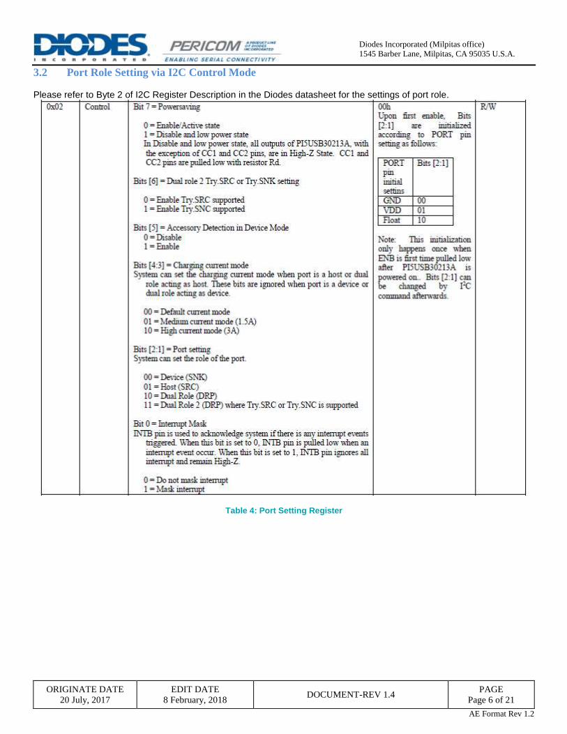
3.2 Port Role Setting via I2C Control Mode
Please refer to Byte 2 of I2C Register Description in the Diodes datasheet for the settings of port role.
Table 4: Port Setting Register
ORIGINATE DATE
20 July, 2017
EDIT DATE
8 February, 2018 DOCUMENT-REV 1.4
PAGE
Page 7 of 21
AE Format Rev 1.2
Diodes Incorporated (Milpitas office)
1545 Barber Lane, Milpitas, CA 95035 U.S.A.
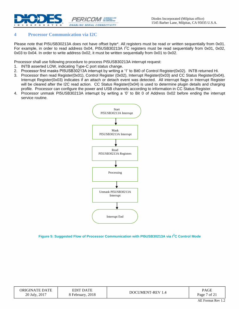
4 Processor Communication via I2C
Please note that PI5USB30213A does not have offset byte*. All registers must be read or written sequentially from 0x01. For example, in order to read address 0x04, PI5USB30213A I
2C registers must be read sequentially from 0x01, 0x02,
0x03 to 0x04. In order to write address 0x02, it must be written sequentially from 0x01 to 0x02. Processor shall use following procedure to process PI5USB30213A interrupt request: 1. INTB asserted LOW, indicating Type-C port status change. 2. Processor first masks PI5USB30213A interrupt by writing a ‘1’ to Bit0 of Control Register(0x02). INTB returned Hi. 3. Processor then read Register(0x01), Control Register (0x02), Interrupt Register(0x03) and CC Status Register(0x04).
Interrupt Register(0x03) indicates if an attach or detach event was detected. All interrupt flags in Interrupt Register will be cleared after the I2C read action. CC Status Register(0x04) is used to determine plugin details and charging profile. Processor can configure the power and USB channels according to information in CC Status Register.
4. Processor unmask PI5USB30213A interrupt by writing a ‘0’ to Bit 0 of Address 0x02 before ending the interrupt service routine.
Figure 5: Suggested Flow of Processor Communication with PI5USB30213A via I2C Control Mode
Start
PI5USB30213A Interrupt
Mask
PI5USB30213A Interrupt
Read PI5USB30213A Registers
Processing
Unmask PI5USB30213A
Interrupt
Interrupt End
ORIGINATE DATE
20 July, 2017
EDIT DATE
8 February, 2018 DOCUMENT-REV 1.4
PAGE
Page 8 of 21
AE Format Rev 1.2
Diodes Incorporated (Milpitas office)
1545 Barber Lane, Milpitas, CA 95035 U.S.A.
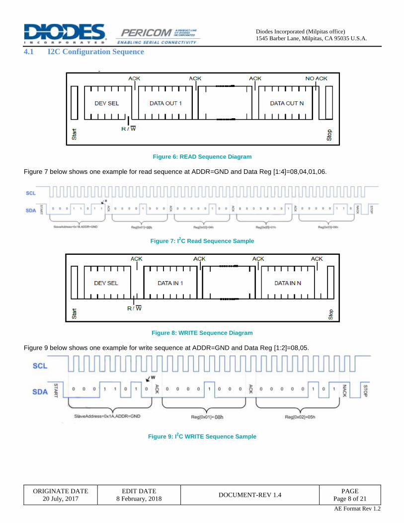
4.1 I2C Configuration Sequence
Figure 6: READ Sequence Diagram
Figure 7 below shows one example for read sequence at ADDR=GND and Data Reg [1:4]=08,04,01,06.
Figure 7: I2C Read Sequence Sample
Figure 8: WRITE Sequence Diagram Figure 9 below shows one example for write sequence at ADDR=GND and Data Reg [1:2]=08,05.
Figure 9: I2C WRITE Sequence Sample
ORIGINATE DATE
20 July, 2017
EDIT DATE
8 February, 2018 DOCUMENT-REV 1.4
PAGE
Page 9 of 21
AE Format Rev 1.2
Diodes Incorporated (Milpitas office)
1545 Barber Lane, Milpitas, CA 95035 U.S.A.
4.2 Power-up Sequence in I2C Control Mode with ENB tied to ground
The power-up sequence for the PI5USB30213A with ENB tied to ground is as following: 1. When system is powered off and PI5USB30213A has no VDD, CC1 and CC2 are pulled low by PI5USB30213A
and the port acts as a UFP/Sink. 2. System powered on and supply VDD to PI5USB30213A. PI5USB30213A is reset by POR. 3. PI5USB30213A in I2C control mode is initialized according to PORT pin setting upon first enable. 4. System first set bit 0 of byte2 to ‘1’ to make sure INTB pin is High. 5. System can change PI5USB30213A to desired mode by writing byte2 according to “Port Setting Register” in
section 3.2. E.g. Write Reg[0x02]=46h to set the port to Try.SNK DRP default current mode. 6. PI5USB30213A monitors CC pins and VBUS for attachment and detachment.
4.3 Power-down and Power-up through ENB pin
The power-down sequence for the PI5USB30213A using ENB is as following: 1. Pull high ENB to disable PI5USB30213A. 2. PI5USB30213A I2C is still accessible and the system should read PI5USB30213A I2C as usual to clean the
interrupt (if any). 3. The device is in disabled state and will pull low CC1 and CC2 and the port acts as a UFP/Sink. 4. User can re-enable the part by pull low ENB pin.
4.4 Power-down and Power-up via Powersaving bit in I2C Control Mode
When ENB is low, user can put PI5USB30213A into low power state via I2C as following: 1. Write Reg[0x02]=81h to put the part in powersaving mode. 2. Read PI5USB30213A I2C to clear byte3 and byte4. 3. The device will also pull low CC1 and CC2 and the port acts as a UFP/Sink. 4 User can re-enable the part by writing desired mode to byte2 according to “Port Setting Register” in section 2.2.
E.g. Write Reg[0x02]=46h to set the port to Try.SNK DRP default current mode.
4.5 I2C Register Quick Reference Table
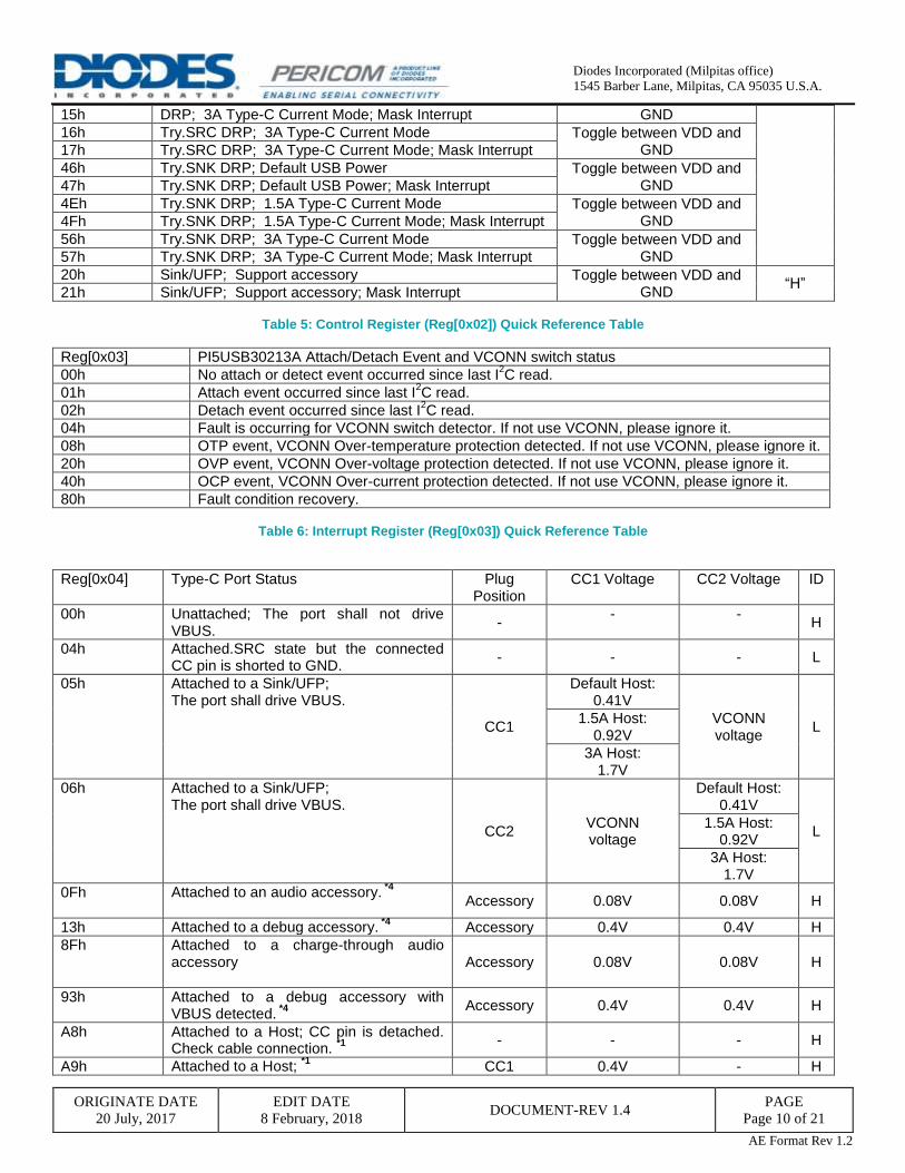
Reg[0x02] PI5USB30213A Operating Mode CC1/2 voltage when unattached
ID pin
00h Sink/UFP; No accessory support GND “H”
01h Sink/UFP; No accessory support; Mask Interrupt
02h Source/DFP; Default USB Power VDD
“L” when UFP is
attached
03h Source/DFP; Default USB Power; Mask Interrupt
04h DRP; Default USB Power Toggle between VDD and GND 05h DRP; Default USB Power; Mask Interrupt
06h Try.SRC DRP; Default USB Power Toggle between VDD and GND 07h Try.SRC DRP; Default USB Power; Mask Interrupt
0Ah Source/DFP; 1.5A Type-C Current Mode VDD
0Bh Source/DFP; 1.5A Type-C Current Mode; Mask Interrupt
0Ch DRP; 1.5A Type-C Current Mode Toggle between VDD and GND 0Dh DRP; 1.5A Type-C Current Mode; Mask Interrupt
0Eh Try.SRC DRP; 1.5A Type-C Current Mode Toggle between VDD and GND 0Fh Try.SRC DRP; 1.5A Type-C Current Mode; Mask Interrupt
12h Source/DFP; 3A Type-C Current Mode VDD
13h Source/DFP; 3A Type-C Current Mode; Mask Interrupt
14h DRP; 3A Type-C Current Mode Toggle between VDD and
ORIGINATE DATE
20 July, 2017
EDIT DATE
8 February, 2018 DOCUMENT-REV 1.4
PAGE
Page 10 of 21
AE Format Rev 1.2
Diodes Incorporated (Milpitas office)
1545 Barber Lane, Milpitas, CA 95035 U.S.A.
15h DRP; 3A Type-C Current Mode; Mask Interrupt GND
16h Try.SRC DRP; 3A Type-C Current Mode Toggle between VDD and GND 17h Try.SRC DRP; 3A Type-C Current Mode; Mask Interrupt
46h Try.SNK DRP; Default USB Power Toggle between VDD and GND 47h Try.SNK DRP; Default USB Power; Mask Interrupt
4Eh Try.SNK DRP; 1.5A Type-C Current Mode Toggle between VDD and GND 4Fh Try.SNK DRP; 1.5A Type-C Current Mode; Mask Interrupt
56h Try.SNK DRP; 3A Type-C Current Mode Toggle between VDD and GND 57h Try.SNK DRP; 3A Type-C Current Mode; Mask Interrupt
20h Sink/UFP; Support accessory Toggle between VDD and GND
“H” 21h Sink/UFP; Support accessory; Mask Interrupt
Table 5: Control Register (Reg[0x02]) Quick Reference Table
Reg[0x03] PI5USB30213A Attach/Detach Event and VCONN switch status
00h No attach or detect event occurred since last I2C read.
01h Attach event occurred since last I2C read.
02h Detach event occurred since last I2C read.
04h Fault is occurring for VCONN switch detector. If not use VCONN, please ignore it.
08h OTP event, VCONN Over-temperature protection detected. If not use VCONN, please ignore it.
20h OVP event, VCONN Over-voltage protection detected. If not use VCONN, please ignore it.
40h OCP event, VCONN Over-current protection detected. If not use VCONN, please ignore it.
04h Attached.SRC state but the connected CC pin is shorted to GND.
- - - L
05h Attached to a Sink/UFP; The port shall drive VBUS.
CC1
Default Host: 0.41V
VCONN voltage
L 1.5A Host:
0.92V
3A Host: 1.7V
06h Attached to a Sink/UFP; The port shall drive VBUS.
CC2 VCONN voltage
Default Host: 0.41V
L 1.5A Host:
0.92V
3A Host: 1.7V
0Fh Attached to an audio accessory. *4
Accessory 0.08V 0.08V H
13h Attached to a debug accessory. *4
Accessory 0.4V 0.4V H
8Fh Attached to a charge-through audio accessory
Accessory 0.08V 0.08V H
93h Attached to a debug accessory with VBUS detected.
*4
Accessory 0.4V 0.4V H
A8h Attached to a Host; CC pin is detached. Check cable connection.
*1
- - - H
A9h Attached to a Host; *1
CC1 0.4V - H
ORIGINATE DATE
20 July, 2017
EDIT DATE
8 February, 2018 DOCUMENT-REV 1.4
PAGE
Page 11 of 21
AE Format Rev 1.2
Diodes Incorporated (Milpitas office)
1545 Barber Lane, Milpitas, CA 95035 U.S.A.
AAh Attached to a Host; *1
CC2 - 0.4V H
C8h Attached to a Host; CC pin is detached. Check cable connection.
*2
- - - H
C9h Attached to a Host; *2
CC1 0.92V - H
CAh Attached to a Host; *2
CC2 - 0.92V H
E8h Attached to a Host; CC pin is detached. Check cable connection.
*3
- - - H
E9h Attached to a Host; *3
CC1 1.7V - H
EAh Attached to a Host; *3
CC2 - 1.7V H
Table 7: CC Status (Reg[0x04]) Quick Reference Table
Note
*1: The port shall draw no more than the default USB power from VBUS. *2: The port shall draw no more than 1.5A from VBUS. *3: The port shall draw no more than 3A from VBUS. *4: According to Type-C spec 1.1, the port shall not drive VBUS. *5: The port shall not sink more than 500mA from VBUS.
ORIGINATE DATE
20 July, 2017
EDIT DATE
8 February, 2018 DOCUMENT-REV 1.4
PAGE
Page 12 of 21
AE Format Rev 1.2
Diodes Incorporated (Milpitas office)
1545 Barber Lane, Milpitas, CA 95035 U.S.A.
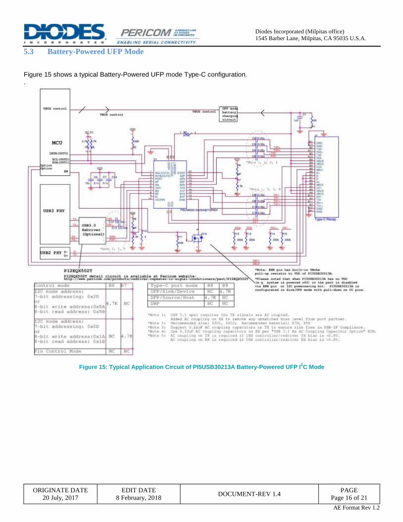
5. Typical Application Circuit
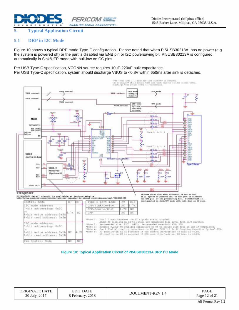
5.1 DRP in I2C Mode Figure 10 shows a typical DRP mode Type-C configuration. Please noted that when PI5USB30213A: has no power (e.g. the system is powered off) or the part is disabled via ENB pin or I2C powersaving bit, PI5USB30213A is configured automatically in Sink/UFP mode with pull-low on CC pins. Per USB Type-C specification, VCONN source requires 10uF-220uF bulk capacitance. Per USB Type-C specification, system should discharge VBUS to <0.8V within 650ms after sink is detached.
Figure 10: Typical Application Circuit of PI5USB30213A DRP I2C Mode
ORIGINATE DATE
20 July, 2017
EDIT DATE
8 February, 2018 DOCUMENT-REV 1.4
PAGE
Page 13 of 21
AE Format Rev 1.2
Diodes Incorporated (Milpitas office)
1545 Barber Lane, Milpitas, CA 95035 U.S.A.
5.2 DFP Mode
5.2.1 DFP in I2C Mode
Figure 11 shows a typical Source/DFP mode Type-C configuration. Per USB Type-C specification, system should discharge VBUS to <0.8V within 650ms after sink is detached. In Source/DFP only mode, shall discharge VBUS within 100ms.
Figure 11: Typical Application Circuit of PI5USB30213A DFP I2C Mode
ORIGINATE DATE
20 July, 2017
EDIT DATE
8 February, 2018 DOCUMENT-REV 1.4
PAGE
Page 14 of 21
AE Format Rev 1.2
Diodes Incorporated (Milpitas office)
1545 Barber Lane, Milpitas, CA 95035 U.S.A.
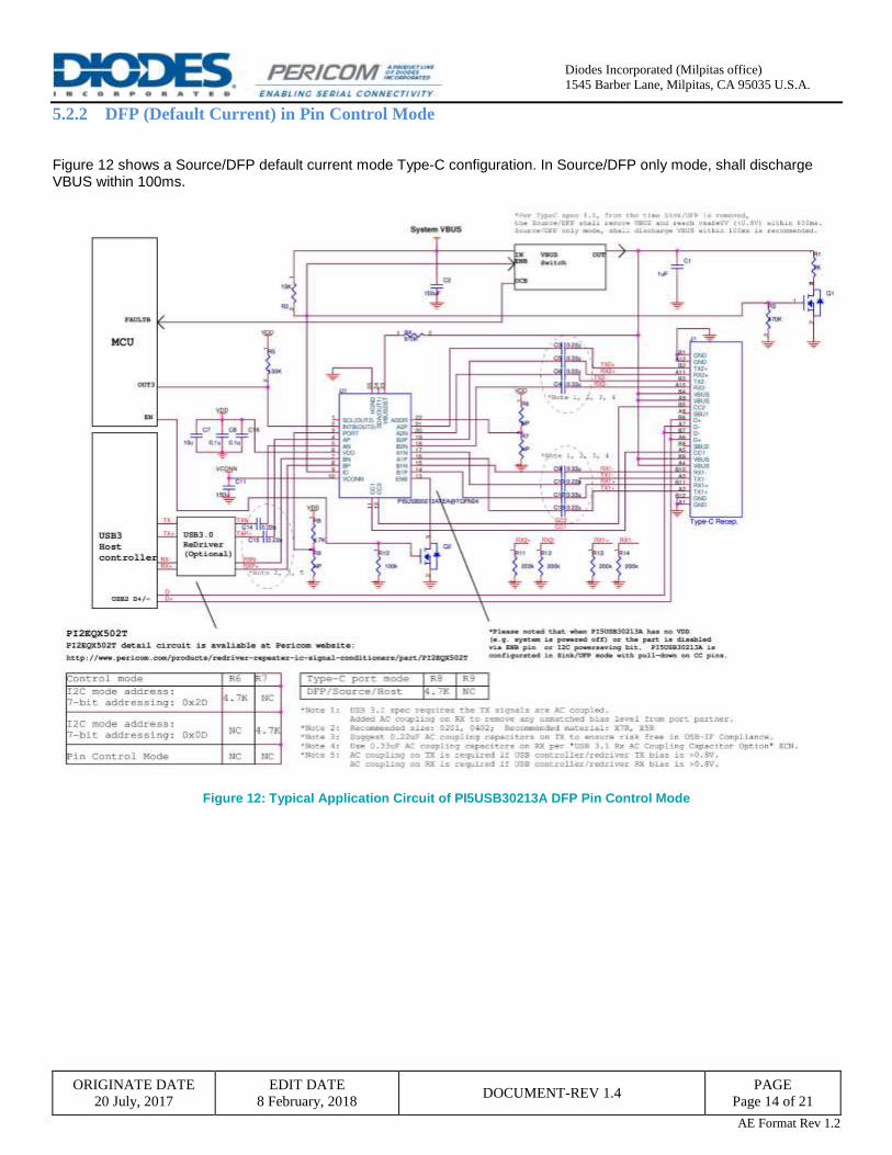
5.2.2 DFP (Default Current) in Pin Control Mode
Figure 12 shows a Source/DFP default current mode Type-C configuration. In Source/DFP only mode, shall discharge VBUS within 100ms.
Figure 12: Typical Application Circuit of PI5USB30213A DFP Pin Control Mode
ORIGINATE DATE
20 July, 2017
EDIT DATE
8 February, 2018 DOCUMENT-REV 1.4
PAGE
Page 15 of 21
AE Format Rev 1.2
Diodes Incorporated (Milpitas office)
1545 Barber Lane, Milpitas, CA 95035 U.S.A.
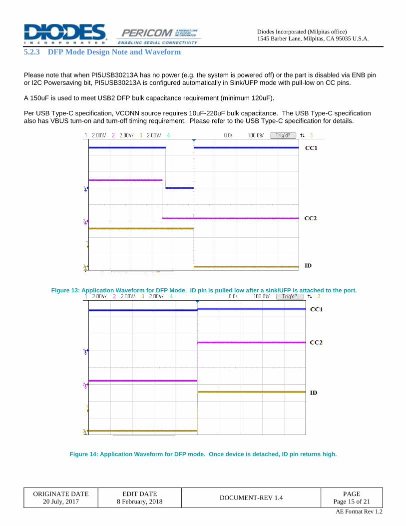
5.2.3 DFP Mode Design Note and Waveform
Please note that when PI5USB30213A has no power (e.g. the system is powered off) or the part is disabled via ENB pin or I2C Powersaving bit, PI5USB30213A is configured automatically in Sink/UFP mode with pull-low on CC pins. A 150uF is used to meet USB2 DFP bulk capacitance requirement (minimum 120uF). Per USB Type-C specification, VCONN source requires 10uF-220uF bulk capacitance. The USB Type-C specification also has VBUS turn-on and turn-off timing requirement. Please refer to the USB Type-C specification for details.
Figure 13: Application Waveform for DFP Mode. ID pin is pulled low after a sink/UFP is attached to the port.
Figure 14: Application Waveform for DFP mode. Once device is detached, ID pin returns high.
At least 1pc 4.7uF and 1pc 0.1uF decoupling capacitors are recommended for VDD of PI5USB30213A. Each decoupling capacitor should be connected to PCB power plane via shortest path. VDD and GND pins should be
shorted to PCB power planes via shortest paths.
At least 1uF decoupling capacitor is recommended at VBUS.
6.2 Layout Example
Typical application Layout suggestion
Use 6/7/6 mils for trace-space-trace for the micro-strip lines (the traces on top and bottom layers) for 90ohm differential impedance.
Use 6/5/6 mils for trace-space-trace for the strip-lines (the traces inside layers) for 90ohm differential impedance. Use FR4. Using standard 4 to 8 layers stack-up with 0.062 inch thick PCB. For micro-strip lines, using ½ OZ Cu plated is ok. For strip-lines in 6 plus players, using 1 OZ Cu is better. The trace length miss-matching shall be less than 5 mils for the “+” and “–“ traces in the same pairs More pair-to-pair spacing for minimal crosstalk
Target differential Zo of 90ohm ±15%
The PCB layout recommended: Use 0.1uf in size of 0402 for all the Vdd (any power pins) pins of the IC device, as close to the Vdd pins as possible,
within 2-3mm if feasible. Use dedicated Vdd and GND planes for to minimize the jitters coupled between channel trough power sources
Figure 16: The Layout Guidance for the trace routings
ORIGINATE DATE
20 July, 2017
EDIT DATE
8 February, 2018 DOCUMENT-REV 1.4
PAGE
Page 18 of 21
AE Format Rev 1.2
Diodes Incorporated (Milpitas office)
1545 Barber Lane, Milpitas, CA 95035 U.S.A.
Figure 17: PI5USB30213A Layout Example
ORIGINATE DATE
20 July, 2017
EDIT DATE
8 February, 2018 DOCUMENT-REV 1.4
PAGE
Page 19 of 21
AE Format Rev 1.2
Diodes Incorporated (Milpitas office)
1545 Barber Lane, Milpitas, CA 95035 U.S.A.
7 Firmware Example
bool vconn_flag = FALSE; //Global Variable for VCONN function flag.
char i2c_read_buf[4]={0x00,0x00,0x00,0x00};
char i2c_write_buf[2]={0x00,0x00};
void PI5USB30213A_INTN_handler (void)
{
char vconn_status = 0x00; //Variable for VCONN switch status;