2013-2014 Microchip Technology Inc. Preliminary DS40001720C-page 1 This document includes the programming specifications for the following devices: 1.0 OVERVIEW The devices can be programmed using either the high-voltage In-Circuit Serial Programming™ (ICSP™) method or the low-voltage ICSP™ method. 1.1 Hardware Requirements 1.1.1 HIGH-VOLTAGE ICSP PROGRAMMING In High-Voltage ICSP™ mode, these devices require two programmable power supplies: one for VDD and one for the MCLR /VPP pin. 1.1.2 LOW-VOLTAGE ICSP PROGRAMMING In Low-Voltage ICSP™ mode, these devices can be programmed using a single VDD source in the operating range. The MCLR /VPP pin does not have to be brought to a different voltage, but can instead be left at the normal operating voltage. 1.1.2.1 Single-Supply ICSP Programming The LVP bit in Configuration Word 2 enables single-supply (low-voltage) ICSP programming. The LVP bit defaults to a ‘1’ (enabled) from the factory. The LVP bit may only be programmed to ‘0’ by entering the High-Voltage ICSP mode, where the MCLR /VPP pin is raised to VIHH. Once the LVP bit is programmed to a ‘0’, only the High-Voltage ICSP mode is available and only the High-Voltage ICSP mode can be used to program the device. • PIC12F1612 • PIC12LF1612 • PIC16F1613 • PIC16LF1613 • PIC16F1614 • PIC16LF1614 • PIC16F1615 • PIC16LF1615 • PIC16F1618 • PIC16LF1618 • PIC16F1619 • PIC16LF1619 Note 1: The High-Voltage ICSP mode is always available, regardless of the state of the LVP bit, by applying VIHH to the MCLR /VPP pin. 2: While in Low-Voltage ICSP mode, MCLR is always enabled, regardless of the MCLRE bit, and the port pin can no longer be used as a general purpose input. PIC12(L)F1612/16(L)F161X Memory Programming Specification PIC12(L)F1612/16(L)F161X
This document includes the programming specifications for the following devices:
1.0 OVERVIEW
The devices can be programmed using either the high-voltage In-Circuit Serial Programming™ (ICSP™) method or thelow-voltage ICSP™ method.
1.1 Hardware Requirements
1.1.1 HIGH-VOLTAGE ICSP PROGRAMMING
In High-Voltage ICSP™ mode, these devices require two programmable power supplies: one for VDD and one for theMCLR/VPP pin.
1.1.2 LOW-VOLTAGE ICSP PROGRAMMING
In Low-Voltage ICSP™ mode, these devices can be programmed using a single VDD source in the operating range. TheMCLR/VPP pin does not have to be brought to a different voltage, but can instead be left at the normal operating voltage.
1.1.2.1 Single-Supply ICSP Programming
The LVP bit in Configuration Word 2 enables single-supply (low-voltage) ICSP programming. The LVP bit defaults to a‘1’ (enabled) from the factory. The LVP bit may only be programmed to ‘0’ by entering the High-Voltage ICSP mode,where the MCLR/VPP pin is raised to VIHH. Once the LVP bit is programmed to a ‘0’, only the High-Voltage ICSP modeis available and only the High-Voltage ICSP mode can be used to program the device.
• PIC12F1612 • PIC12LF1612
• PIC16F1613 • PIC16LF1613
• PIC16F1614 • PIC16LF1614
• PIC16F1615 • PIC16LF1615
• PIC16F1618 • PIC16LF1618
• PIC16F1619 • PIC16LF1619
Note 1: The High-Voltage ICSP mode is always available, regardless of the state of the LVP bit, by applying VIHH
to the MCLR/VPP pin.
2: While in Low-Voltage ICSP mode, MCLR is always enabled, regardless of the MCLRE bit, and the portpin can no longer be used as a general purpose input.
2013-2014 Microchip Technology Inc. Preliminary DS40001720C-page 1
PIC12(L)F1612/16(L)F161X
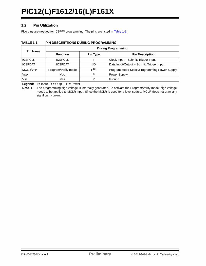
1.2 Pin Utilization
Five pins are needed for ICSP™ programming. The pins are listed in Table 1-1.
TABLE 1-1: PIN DESCRIPTIONS DURING PROGRAMMING
Pin NameDuring Programming
Function Pin Type Pin Description
ICSPCLK ICSPCLK I Clock Input – Schmitt Trigger Input
ICSPDAT ICSPDAT I/O Data Input/Output – Schmitt Trigger Input
MCLR/VPP Program/Verify mode P(1) Program Mode Select/Programming Power Supply
VDD VDD P Power Supply
VSS VSS P Ground
Legend: I = Input, O = Output, P = PowerNote 1: The programming high voltage is internally generated. To activate the Program/Verify mode, high voltage
needs to be applied to MCLR input. Since the MCLR is used for a level source, MCLR does not draw any significant current.
DS40001720C-page 2 Preliminary 2013-2014 Microchip Technology Inc.
PIC12(L)F1612/16(L)F161X
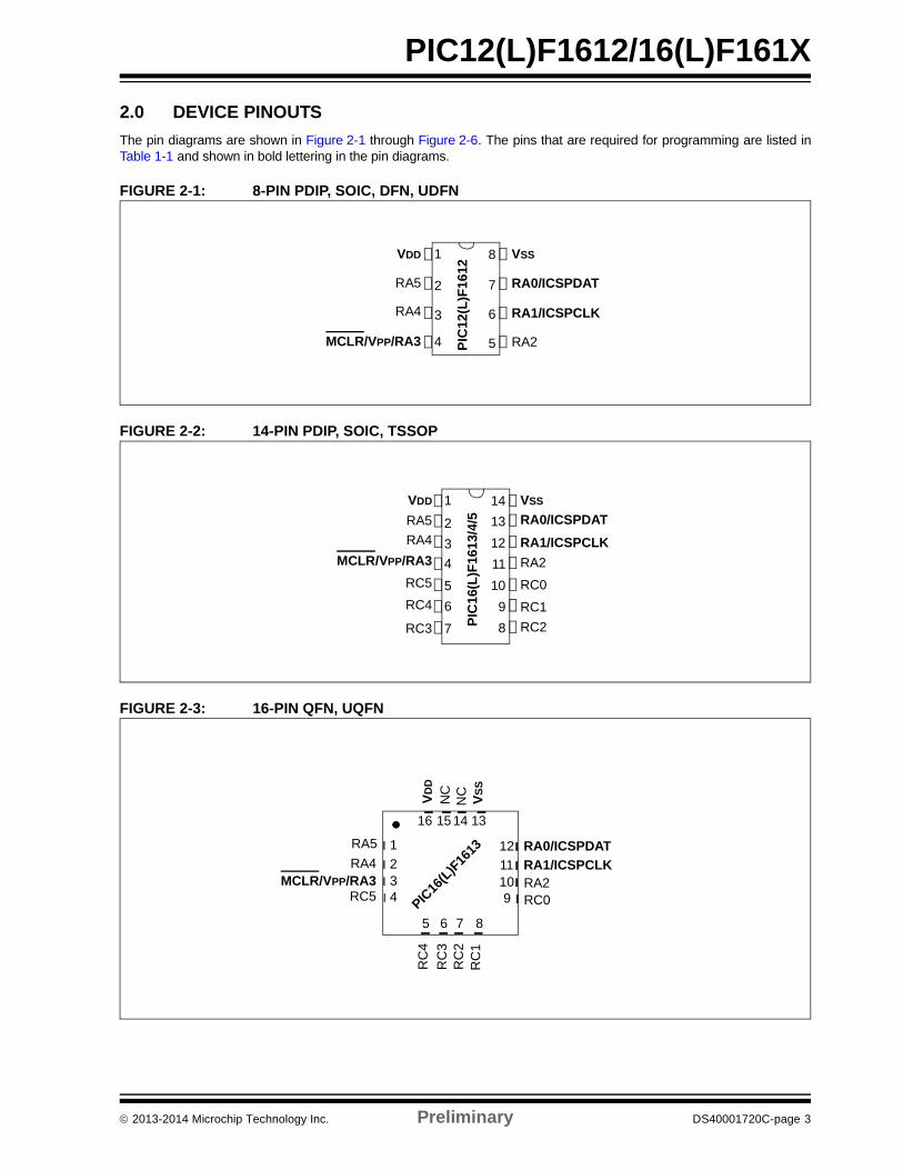
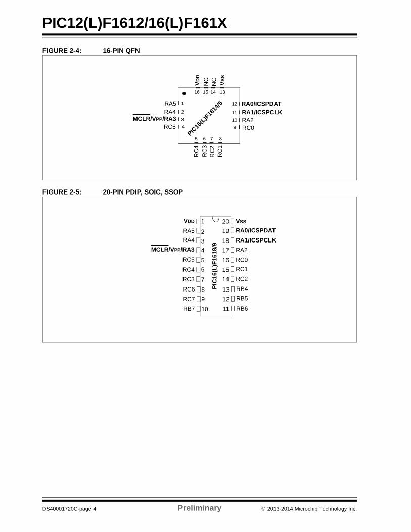
2.0 DEVICE PINOUTS
The pin diagrams are shown in Figure 2-1 through Figure 2-6. The pins that are required for programming are listed inTable 1-1 and shown in bold lettering in the pin diagrams.
FIGURE 2-1: 8-PIN PDIP, SOIC, DFN, UDFN
FIGURE 2-2: 14-PIN PDIP, SOIC, TSSOP
FIGURE 2-3: 16-PIN QFN, UQFN
1
2
3
4
8
7
6
5
VDD
RA5
RA4
MCLR/VPP/RA3
VSS
RA0/ICSPDAT
RA1/ICSPCLK
RA2PIC
12(L
)F1
612
PIC
16(
L)F
161
3/4
/5
1
2
3
4
14
13
12
11
5
6
7
10
9
8
VDD
RA5
RA4
MCLR/VPP/RA3
RC5
RC4
RC3
VSS
RA0/ICSPDAT
RA1/ICSPCLK
RA2
RC0
RC1
RC2
7 8
23
1
11
12
5
910
13141516
6
4
RA5
RA4MCLR/VPP/RA3
RC
4
RC
3
RC
1R
C2
RA0/ICSPDAT
RA2RA1/ICSPCLK
VS
S
VD
D
NC
RC5
NC
PIC16
(L)F
1613
RC0
2013-2014 Microchip Technology Inc. Preliminary DS40001720C-page 3
PIC12(L)F1612/16(L)F161X
FIGURE 2-4: 16-PIN QFN
FIGURE 2-5: 20-PIN PDIP, SOIC, SSOP
7 8
2
3
1
11
12
5
9
10
13141516
6
4
RA5RA4
RC
4R
C3
RC
1R
C2
RC0
RA0/ICSPDAT
RA2RA1/ICSPCLK
VS
S
VD
D
NC
RC5
NC
PIC16
(L)F
1614
/5
MCLR/VPP/RA3
PIC
16(
L)F
161
8/9
1
2
3
4
20
19
18
17
5
6
7
16
15
14
VDD
RA5
RA4
MCLR/VPP/RA3
RC5
RC4
RC3
VSS
RA0/ICSPDAT
RA1/ICSPCLK
RA2
RC0
RC1
RC2
8
9
10
13
12
11
RC6
RC7
RB7
RB4
RB5
RB6
DS40001720C-page 4 Preliminary 2013-2014 Microchip Technology Inc.
PIC12(L)F1612/16(L)F161X
FIGURE 2-6: 20-PIN QFN
8 9
23
1
14
16
106
17181920
7
54
PIC16
(L)F
1618
/9MCLR/VPP/RA3
RC5RC4RC3RC6
RC
7R
B7
RB
4R
B5
RB
6
RA
0/I
CS
PD
AT
VS
S
VD
D
RA
4R
A5
111213
RC1RC0
RC2
15 RA1/ICSPCLKRA2
2013-2014 Microchip Technology Inc. Preliminary DS40001720C-page 5
PIC12(L)F1612/16(L)F161X
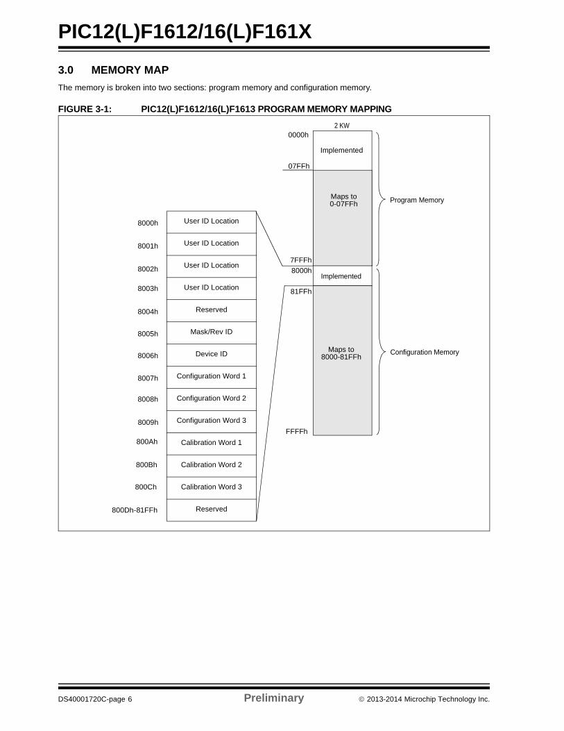
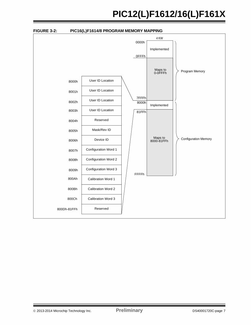
3.0 MEMORY MAP
The memory is broken into two sections: program memory and configuration memory.
FIGURE 3-1: PIC12(L)F1612/16(L)F1613 PROGRAM MEMORY MAPPING
7FFFh
8000h
81FFh
FFFFh
2 KW
Implemented
Maps to
Program Memory
Configuration Memory8000-81FFh
User ID Location
User ID Location
User ID Location
User ID Location
Reserved
Mask/Rev ID
Device ID
Configuration Word 1
Configuration Word 2
Configuration Word 3
Calibration Word 1
Calibration Word 2
Calibration Word 3
Reserved
8000h
8001h
8002h
8003h
8004h
8005h
8006h
8007h
8009h
8008h
800Ah
Implemented
0000h
Maps to0-07FFh
07FFh
800Dh-81FFh
800Bh
800Ch
DS40001720C-page 6 Preliminary 2013-2014 Microchip Technology Inc.
PIC12(L)F1612/16(L)F161X
FIGURE 3-2: PIC16(L)F1614/8 PROGRAM MEMORY MAPPING
7FFFh
8000h
81FFh
FFFFh
4 KW
Implemented
Maps to
Program Memory
Configuration Memory8000-81FFh
User ID Location
User ID Location
User ID Location
User ID Location
Reserved
Mask/Rev ID
Device ID
Configuration Word 1
Configuration Word 2
Configuration Word 3
Calibration Word 1
Calibration Word 2
Calibration Word 3
Reserved
8000h
8001h
8002h
8003h
8004h
8005h
8006h
8007h
8009h
8008h
800Ah
Implemented
0000h
Maps to0-0FFFh
0FFFh
800Dh-81FFh
800Bh
800Ch
2013-2014 Microchip Technology Inc. Preliminary DS40001720C-page 7
PIC12(L)F1612/16(L)F161X
FIGURE 3-3: PIC16(L)F1615/9 PROGRAM MEMORY MAPPING
7FFFh
8000h
81FFh
FFFFh
8 KW
Implemented
Maps to
Program Memory
Configuration Memory8000-81FFh
User ID Location
User ID Location
User ID Location
User ID Location
Reserved
Mask/Rev ID
Device ID
Configuration Word 1
Configuration Word 2
Configuration Word 3
Calibration Word 1
Calibration Word 2
Calibration Word 3
Reserved
8000h
8001h
8002h
8003h
8004h
8005h
8006h
8007h
8009h
8008h
800Ah
Implemented
0000h
Maps to0-1FFFh
1FFFh
800Dh-81FFh
800Bh
800Ch
DS40001720C-page 8 Preliminary 2013-2014 Microchip Technology Inc.
PIC12(L)F1612/16(L)F161X
3.1 User ID Location
A user may store identification information (user ID) in four designated locations. The user ID locations are mapped to8000h-8003h. Each location is 14 bits in length. Code protection has no effect on these memory locations. Each locationmay be read with code protection enabled or disabled.
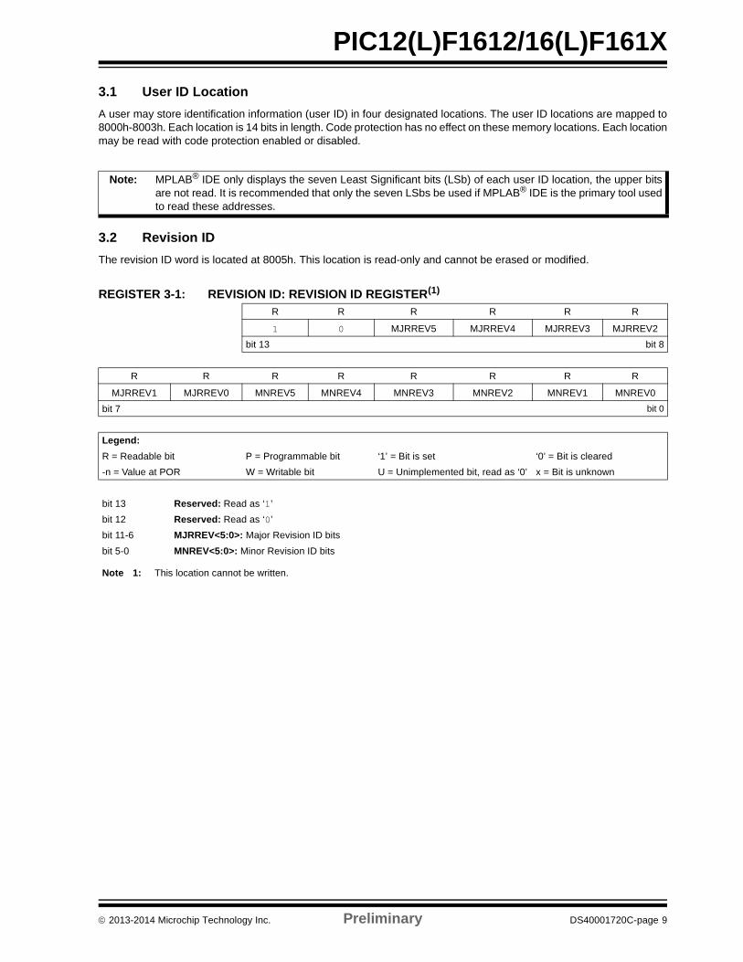
3.2 Revision ID
The revision ID word is located at 8005h. This location is read-only and cannot be erased or modified.
Note: MPLAB® IDE only displays the seven Least Significant bits (LSb) of each user ID location, the upper bitsare not read. It is recommended that only the seven LSbs be used if MPLAB® IDE is the primary tool usedto read these addresses.
REGISTER 3-1: REVISION ID: REVISION ID REGISTER(1)
R = Readable bit P = Programmable bit ‘1’ = Bit is set ‘0’ = Bit is cleared
-n = Value at POR W = Writable bit U = Unimplemented bit, read as ‘0’ x = Bit is unknown
bit 13 Reserved: Read as ‘1’
bit 12 Reserved: Read as ‘0’
bit 11-6 MJRREV<5:0>: Major Revision ID bits
bit 5-0 MNREV<5:0>: Minor Revision ID bits
Note 1: This location cannot be written.
2013-2014 Microchip Technology Inc. Preliminary DS40001720C-page 9
PIC12(L)F1612/16(L)F161X
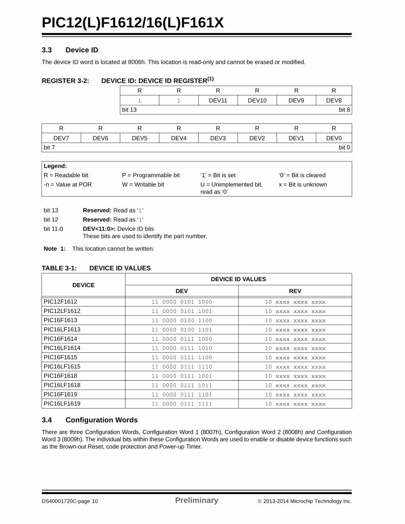
3.3 Device ID
The device ID word is located at 8006h. This location is read-only and cannot be erased or modified.
3.4 Configuration Words
There are three Configuration Words, Configuration Word 1 (8007h), Configuration Word 2 (8008h) and ConfigurationWord 3 (8009h). The individual bits within these Configuration Words are used to enable or disable device functions suchas the Brown-out Reset, code protection and Power-up Timer.
REGISTER 3-2: DEVICE ID: DEVICE ID REGISTER(1)
R R R R R R
1 1 DEV11 DEV10 DEV9 DEV8
bit 13 bit 8
R R R R R R R R
DEV7 DEV6 DEV5 DEV4 DEV3 DEV2 DEV1 DEV0
bit 7 bit 0
Legend:
R = Readable bit P = Programmable bit ‘1’ = Bit is set ‘0’ = Bit is cleared
-n = Value at POR W = Writable bit U = Unimplemented bit, read as ‘0’
x = Bit is unknown
bit 13 Reserved: Read as ‘1’
bit 12 Reserved: Read as ‘1’
bit 11-0 DEV<11:0>: Device ID bitsThese bits are used to identify the part number.
Note 1: This location cannot be written.
TABLE 3-1: DEVICE ID VALUES
DEVICEDEVICE ID VALUES
DEV REV
PIC12F1612 11 0000 0101 1000 10 xxxx xxxx xxxx
PIC12LF1612 11 0000 0101 1001 10 xxxx xxxx xxxx
PIC16F1613 11 0000 0100 1100 10 xxxx xxxx xxxx
PIC16LF1613 11 0000 0100 1101 10 xxxx xxxx xxxx
PIC16F1614 11 0000 0111 1000 10 xxxx xxxx xxxx
PIC16LF1614 11 0000 0111 1010 10 xxxx xxxx xxxx
PIC16F1615 11 0000 0111 1100 10 xxxx xxxx xxxx
PIC16LF1615 11 0000 0111 1110 10 xxxx xxxx xxxx
PIC16F1618 11 0000 0111 1001 10 xxxx xxxx xxxx
PIC16LF1618 11 0000 0111 1011 10 xxxx xxxx xxxx
PIC16F1619 11 0000 0111 1101 10 xxxx xxxx xxxx
PIC16LF1619 11 0000 0111 1111 10 xxxx xxxx xxxx
DS40001720C-page 10 Preliminary 2013-2014 Microchip Technology Inc.
PIC12(L)F1612/16(L)F161X
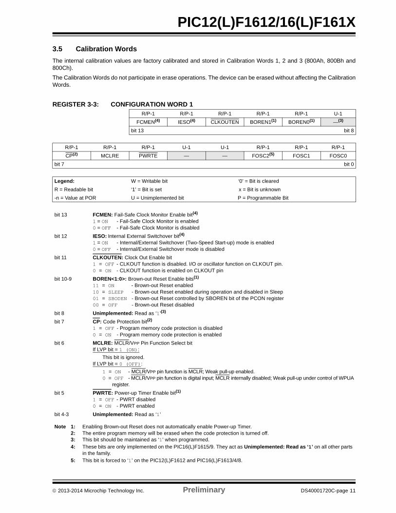
3.5 Calibration Words
The internal calibration values are factory calibrated and stored in Calibration Words 1, 2 and 3 (800Ah, 800Bh and800Ch).
The Calibration Words do not participate in erase operations. The device can be erased without affecting the CalibrationWords.
R = Readable bit ‘1’ = Bit is set x = Bit is unknown
-n = Value at POR U = Unimplemented bit P = Programmable Bit
bit 13 FCMEN: Fail-Safe Clock Monitor Enable bit(4)
1 = ON - Fail-Safe Clock Monitor is enabled0 = OFF - Fail-Safe Clock Monitor is disabled
bit 12 IESO: Internal External Switchover bit(4)
1 = ON - Internal/External Switchover (Two-Speed Start-up) mode is enabled0 = OFF - Internal/External Switchover mode is disabled
bit 11 CLKOUTEN: Clock Out Enable bit1 = OFF - CLKOUT function is disabled. I/O or oscillator function on CLKOUT pin.0 = ON - CLKOUT function is enabled on CLKOUT pin
bit 10-9 BOREN<1:0>: Brown-out Reset Enable bits(1)
11 = ON - Brown-out Reset enabled10 = SLEEP - Brown-out Reset enabled during operation and disabled in Sleep01 = SBODEN - Brown-out Reset controlled by SBOREN bit of the PCON register00 = OFF - Brown-out Reset disabled
bit 8 Unimplemented: Read as ‘1’(3)
bit 7 CP: Code Protection bit(2)
1 = OFF - Program memory code protection is disabled0 = ON - Program memory code protection is enabled
bit 6 MCLRE: MCLR/VPP Pin Function Select bitIf LVP bit = 1 (ON):
This bit is ignored.If LVP bit = 0 (OFF):
1 = ON - MCLR/VPP pin function is MCLR; Weak pull-up enabled.0 = OFF - MCLR/VPP pin function is digital input; MCLR internally disabled; Weak pull-up under control of WPUA
register.
bit 5 PWRTE: Power-up Timer Enable bit(1)
1 = OFF - PWRT disabled0 = ON - PWRT enabled
bit 4-3 Unimplemented: Read as ‘1’
Note 1: Enabling Brown-out Reset does not automatically enable Power-up Timer.2: The entire program memory will be erased when the code protection is turned off.3: This bit should be maintained as ‘1’ when programmed.4: These bits are only implemented on the PIC16(L)F1615/9. They act as Unimplemented: Read as ‘1’ on all other parts
in the family.5: This bit is forced to ‘1’ on the PIC12(L)F1612 and PIC16(L)F1613/4/8.
2013-2014 Microchip Technology Inc. Preliminary DS40001720C-page 11
PIC12(L)F1612/16(L)F161X
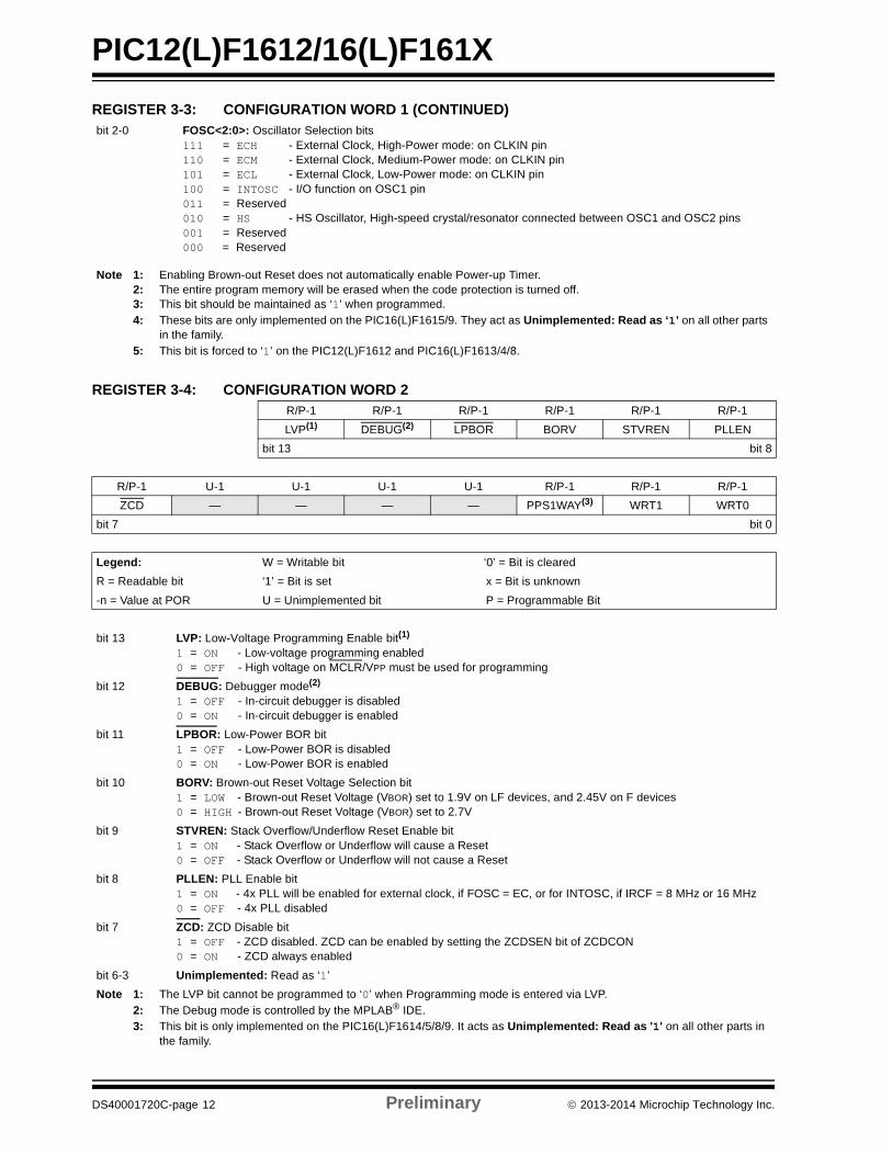
bit 2-0 FOSC<2:0>: Oscillator Selection bits111 = ECH - External Clock, High-Power mode: on CLKIN pin110 = ECM - External Clock, Medium-Power mode: on CLKIN pin101 = ECL - External Clock, Low-Power mode: on CLKIN pin100 = INTOSC - I/O function on OSC1 pin011 = Reserved010 = HS - HS Oscillator, High-speed crystal/resonator connected between OSC1 and OSC2 pins001 = Reserved000 = Reserved
R = Readable bit ‘1’ = Bit is set x = Bit is unknown
-n = Value at POR U = Unimplemented bit P = Programmable Bit
bit 13 LVP: Low-Voltage Programming Enable bit(1)
1 = ON - Low-voltage programming enabled0 = OFF - High voltage on MCLR/VPP must be used for programming
bit 12 DEBUG: Debugger mode(2)
1 = OFF - In-circuit debugger is disabled0 = ON - In-circuit debugger is enabled
bit 11 LPBOR: Low-Power BOR bit1 = OFF - Low-Power BOR is disabled0 = ON - Low-Power BOR is enabled
bit 10 BORV: Brown-out Reset Voltage Selection bit1 = LOW - Brown-out Reset Voltage (VBOR) set to 1.9V on LF devices, and 2.45V on F devices0 = HIGH - Brown-out Reset Voltage (VBOR) set to 2.7V
bit 9 STVREN: Stack Overflow/Underflow Reset Enable bit1 = ON - Stack Overflow or Underflow will cause a Reset0 = OFF - Stack Overflow or Underflow will not cause a Reset
bit 8 PLLEN: PLL Enable bit1 = ON - 4x PLL will be enabled for external clock, if FOSC = EC, or for INTOSC, if IRCF = 8 MHz or 16 MHz0 = OFF - 4x PLL disabled
bit 7 ZCD: ZCD Disable bit1 = OFF - ZCD disabled. ZCD can be enabled by setting the ZCDSEN bit of ZCDCON 0 = ON - ZCD always enabled
bit 6-3 Unimplemented: Read as ‘1’
Note 1: The LVP bit cannot be programmed to ‘0’ when Programming mode is entered via LVP.2: The Debug mode is controlled by the MPLAB® IDE.3: This bit is only implemented on the PIC16(L)F1614/5/8/9. It acts as Unimplemented: Read as '1' on all other parts in
the family.
REGISTER 3-3: CONFIGURATION WORD 1 (CONTINUED)
Note 1: Enabling Brown-out Reset does not automatically enable Power-up Timer.2: The entire program memory will be erased when the code protection is turned off.3: This bit should be maintained as ‘1’ when programmed.4: These bits are only implemented on the PIC16(L)F1615/9. They act as Unimplemented: Read as ‘1’ on all other parts
in the family.5: This bit is forced to ‘1’ on the PIC12(L)F1612 and PIC16(L)F1613/4/8.
DS40001720C-page 12 Preliminary 2013-2014 Microchip Technology Inc.
PIC12(L)F1612/16(L)F161X
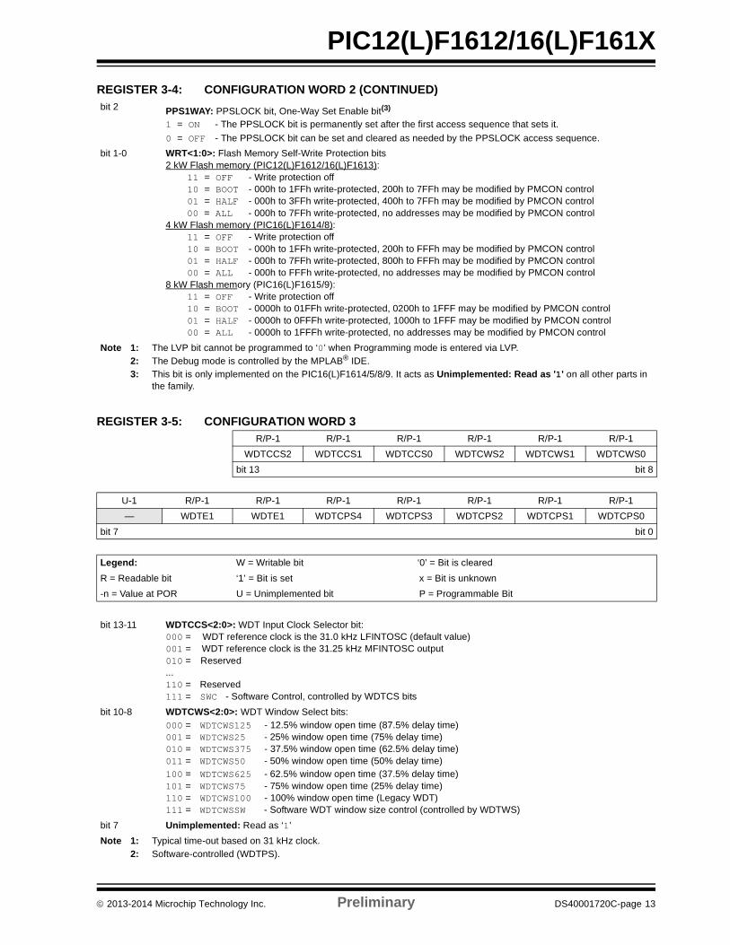
bit 2 PPS1WAY: PPSLOCK bit, One-Way Set Enable bit(3)
1 = ON - The PPSLOCK bit is permanently set after the first access sequence that sets it.
0 = OFF - The PPSLOCK bit can be set and cleared as needed by the PPSLOCK access sequence.
11 = OFF - Write protection off10 = BOOT - 000h to 1FFh write-protected, 200h to 7FFh may be modified by PMCON control01 = HALF - 000h to 3FFh write-protected, 400h to 7FFh may be modified by PMCON control00 = ALL - 000h to 7FFh write-protected, no addresses may be modified by PMCON control
4 kW Flash memory (PIC16(L)F1614/8):11 = OFF - Write protection off10 = BOOT - 000h to 1FFh write-protected, 200h to FFFh may be modified by PMCON control01 = HALF - 000h to 7FFh write-protected, 800h to FFFh may be modified by PMCON control00 = ALL - 000h to FFFh write-protected, no addresses may be modified by PMCON control
8 kW Flash memory (PIC16(L)F1615/9):11 = OFF - Write protection off10 = BOOT - 0000h to 01FFh write-protected, 0200h to 1FFF may be modified by PMCON control01 = HALF - 0000h to 0FFFh write-protected, 1000h to 1FFF may be modified by PMCON control00 = ALL - 0000h to 1FFFh write-protected, no addresses may be modified by PMCON control
R = Readable bit ‘1’ = Bit is set x = Bit is unknown
-n = Value at POR U = Unimplemented bit P = Programmable Bit
bit 13-11 WDTCCS<2:0>: WDT Input Clock Selector bit:000 = WDT reference clock is the 31.0 kHz LFINTOSC (default value)001 = WDT reference clock is the 31.25 kHz MFINTOSC output010 = Reserved...110 = Reserved111 = SWC - Software Control, controlled by WDTCS bits
bit 10-8 WDTCWS<2:0>: WDT Window Select bits:000 = WDTCWS125 - 12.5% window open time (87.5% delay time)001 = WDTCWS25 - 25% window open time (75% delay time)010 = WDTCWS375 - 37.5% window open time (62.5% delay time)011 = WDTCWS50 - 50% window open time (50% delay time)100 = WDTCWS625 - 62.5% window open time (37.5% delay time)101 = WDTCWS75 - 75% window open time (25% delay time)110 = WDTCWS100 - 100% window open time (Legacy WDT)111 = WDTCWSSW - Software WDT window size control (controlled by WDTWS)
bit 7 Unimplemented: Read as ‘1’
Note 1: Typical time-out based on 31 kHz clock.2: Software-controlled (WDTPS).
REGISTER 3-4: CONFIGURATION WORD 2 (CONTINUED)
Note 1: The LVP bit cannot be programmed to ‘0’ when Programming mode is entered via LVP.2: The Debug mode is controlled by the MPLAB® IDE.3: This bit is only implemented on the PIC16(L)F1614/5/8/9. It acts as Unimplemented: Read as '1' on all other parts in
the family.
2013-2014 Microchip Technology Inc. Preliminary DS40001720C-page 13
PIC12(L)F1612/16(L)F161X
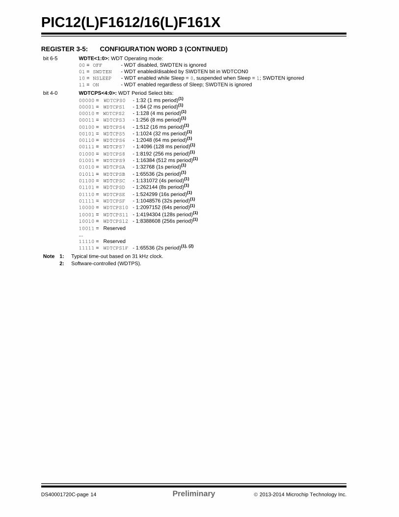
bit 6-5 WDTE<1:0>: WDT Operating mode:00 = OFF - WDT disabled, SWDTEN is ignored01 = SWDTEN - WDT enabled/disabled by SWDTEN bit in WDTCON010 = NSLEEP - WDT enabled while Sleep = 0, suspended when Sleep = 1; SWDTEN ignored11 = ON - WDT enabled regardless of Sleep; SWDTEN is ignored
bit 4-0 WDTCPS<4:0>: WDT Period Select bits:00000 = WDTCPS0 - 1:32 (1 ms period)(1)
Note 1: Typical time-out based on 31 kHz clock.2: Software-controlled (WDTPS).
DS40001720C-page 14 Preliminary 2013-2014 Microchip Technology Inc.
PIC12(L)F1612/16(L)F161X
4.0 PROGRAM/VERIFY MODE
In Program/Verify mode, the program memory and the configuration memory can be accessed and programmed inserial fashion. ICSPDAT and ICSPCLK are used for the data and the clock, respectively. All commands and datawords are transmitted LSb first. Data changes on the rising edge of the ICSPCLK and is latched on the falling edge.In Program/Verify mode both the ICSPDAT and ICSPCLK are Schmitt Trigger inputs. The sequence that enters thedevice into Program/Verify mode places all other logic into the Reset state. Upon entering Program/Verify mode, allI/Os are automatically configured as high-impedance inputs and the address is cleared.
4.1 High-Voltage Program/Verify Mode Entry and Exit
There are two different methods of entering Program/Verify mode via high voltage:
• VPP – First entry mode
• VDD – First entry mode
4.1.1 VPP – FIRST ENTRY MODE
To enter Program/Verify mode via the VPP-first method the following sequence must be followed:
1. Hold ICSPCLK and ICSPDAT low. All other pins should be unpowered.
2. Raise the voltage on MCLR from 0V to VIHH.
3. Raise the voltage on VDD from 0V to the desired operating voltage.
The VPP-first entry prevents the device from executing code prior to entering Program/Verify mode. For example, thedevice will execute code when Configuration Word 1 has MCLR disabled (MCLRE = 0), the Power-up Timer is disabled(PWRTE = 0), the internal oscillator is selected (FOSC = 100), and ICSPCLK and ICSPDAT pins are driven by the userapplication. Since this may prevent entry, VPP-first entry mode is strongly recommended. See the timing diagram inFigure 8-2.
4.1.2 VDD – FIRST ENTRY MODE
To enter Program/Verify mode via the VDD-first method the following sequence must be followed:
1. Hold ICSPCLK and ICSPDAT low.
2. Raise the voltage on VDD from 0V to the desired operating voltage.
3. Raise the voltage on MCLR from VDD or below to VIHH.
The VDD-first method is useful when programming the device when VDD is already applied, for it is not necessary todisconnect VDD to enter Program/Verify mode. See the timing diagram in Figure 8-1.
4.1.3 PROGRAM/VERIFY MODE EXIT
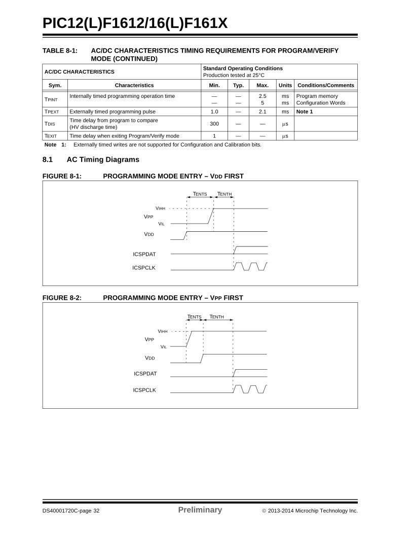
To exit Program/Verify mode take MCLR to VDD or lower (VIL). See Figure 8-3 and Figure 8-4.
Note: In systems where the VDD and MCLR/VPP signals can be controlled independently, the VPP-last methodof exit should be used to keep the device in Reset, thereby preventing any issues that may be caused byprogram execution.
2013-2014 Microchip Technology Inc. Preliminary DS40001720C-page 15
PIC12(L)F1612/16(L)F161X
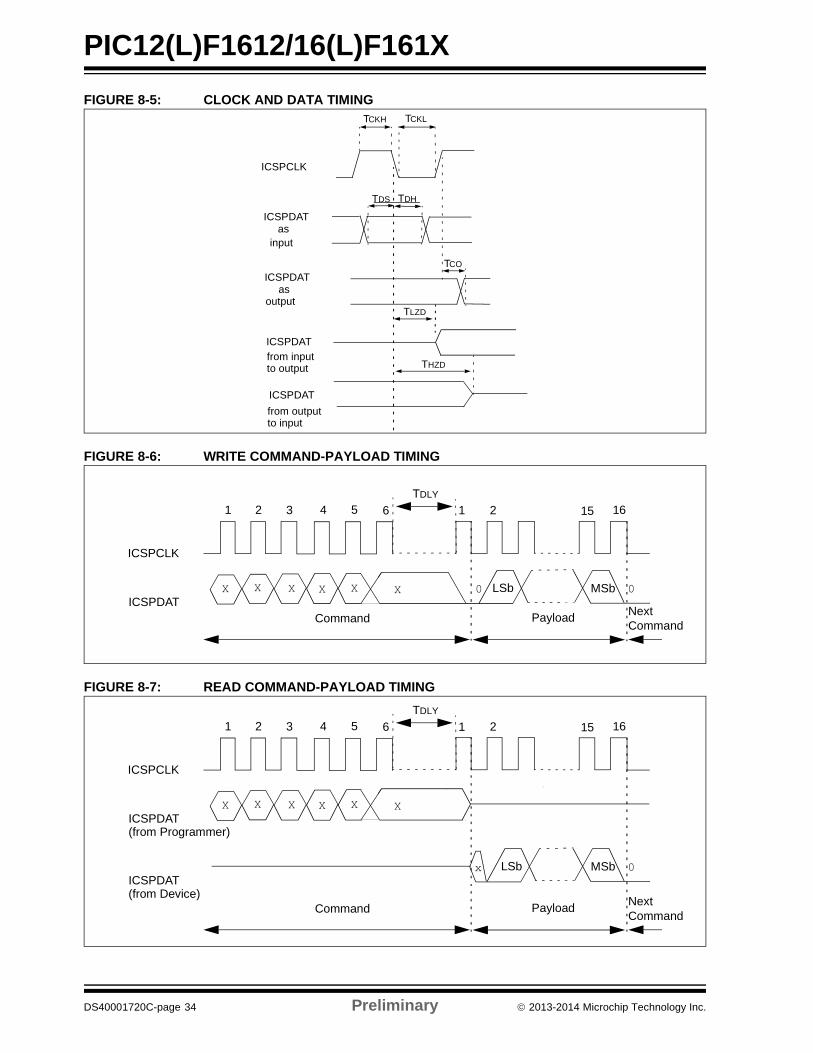
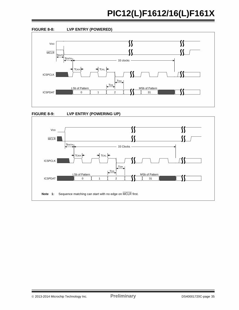
4.2 Low-Voltage Programming (LVP) Mode
The Low-Voltage Programming mode allows devices to be programmed using VDD only, without high voltage. When theLVP bit of Configuration Word 2 register is set to ‘1’, the low-voltage ICSP programming entry is enabled. To disable theLow-Voltage ICSP mode, the LVP bit must be programmed to ‘0’. This can only be done while in the High-Voltage Entrymode.
Entry into the Low-Voltage ICSP Program/Verify modes requires the following steps:
1. MCLR is brought to VIL.
2. A 32-bit key sequence is presented on ICSPDAT, while clocking ICSPCLK.
The key sequence is a specific 32-bit pattern, '0100 1101 0100 0011 0100 1000 0101 0000' (more easilyremembered as MCHP in ASCII). The device will enter Program/Verify mode only if the sequence is valid. The LeastSignificant bit of the Least Significant nibble must be shifted in first.
Once the key sequence is complete, MCLR must be held at VIL for as long as Program/Verify mode is to be maintained.
For low-voltage programming timing, see Figure 8-8 and Figure 8-9.
Exiting Program/Verify mode is done by no longer driving MCLR to VIL. See Figure 8-8 and Figure 8-9.
Note: To enter LVP mode, the LSB of the Least Significant nibble must be shifted in first. This differs from enteringthe key sequence on other parts.
DS40001720C-page 16 Preliminary 2013-2014 Microchip Technology Inc.
PIC12(L)F1612/16(L)F161X
4.3 Program/Verify Commands
The devices implement ten programming commands; each six bits in length. The commands are summarized in Table 4-1.
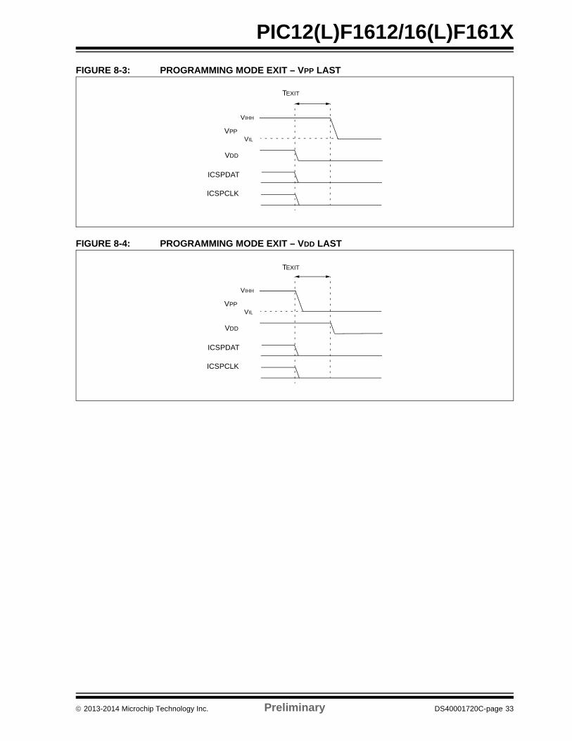
Commands that have data associated with them are specified to have a minimum delay of TDLY between the commandand the data. After this delay 16 clocks are required to either clock in or clock out the 14-bit data word. The first clock isfor the Start bit and the last clock is for the Stop bit.
4.3.1 LOAD CONFIGURATION
The Load Configuration command is used to access the configuration memory (user ID locations, Configuration Words,Calibration Words). The Load Configuration command sets the address to 8000h and loads the data latches with oneword of data (see Figure 4-1).
After issuing the Load Configuration command, use the Increment Address command until the proper address to beprogrammed is reached. The address is then programmed by issuing either the Begin Internally Timed Programming orBegin Externally Timed Programming command.
The only way to get back to the program memory (address 0) is to exit Program/Verify mode or issue the Reset Addresscommand after the configuration memory has been accessed by the Load Configuration command.
FIGURE 4-1: LOAD CONFIGURATION
TABLE 4-1: COMMAND MAPPING
CommandMapping Data/Note
Binary (MSb … LSb) Hex
Load Configuration x 0 0 0 0 0 00h 0, data (14), 0
Load Data For Program Memory x 0 0 0 1 0 02h 0, data (14), 0
Read Data From Program Memory x 0 0 1 0 0 04h 0, data (14), 0
Increment Address x 0 0 1 1 0 06h —
Reset Address x 1 0 1 1 0 16h —
Begin Internally Timed Programming x 0 1 0 0 0 08h —
Begin Externally Timed Programming x 1 1 0 0 0 18h —
End Externally Timed Programming x 0 1 0 1 0 0Ah —
Bulk Erase Program Memory x 0 1 0 0 1 09h Internally Timed
Row Erase Program Memory x 1 0 0 0 1 11h Internally Timed
Note: Externally timed writes are not supported for Configuration and Calibration bits. Any externally timed writeto the Configuration or Calibration Word will have no effect on the targeted word.
X0 0 LSb MSb 0
1 2 3 4 5 6 1 2 15 16
ICSPCLK
ICSPDAT0 0 0 0
TDLY
2013-2014 Microchip Technology Inc. Preliminary DS40001720C-page 17
PIC12(L)F1612/16(L)F161X
4.3.2 LOAD DATA FOR PROGRAM MEMORY
The Load Data for Program Memory command is used to load one 14-bit word into thedata latches. The word programs into program memory after the Begin Internally Timed Programming or BeginExternally Timed Programming command is issued (see Figure 4-2).
FIGURE 4-2: LOAD DATA FOR PROGRAM MEMORY
4.3.3 READ DATA FROM PROGRAM MEMORY
The Read Data from Program Memory command will transmit data bits out of the program memory map currentlyaccessed, starting with the second rising edge of the clock input. The ICSPDAT pin will go into Output mode on the firstfalling clock edge, and it will revert to Input mode (high-impedance) after the 16th falling edge of the clock. If the programmemory is code-protected (CP), the data will be read as zeros (see Figure 4-3).
FIGURE 4-3: READ DATA FROM PROGRAM MEMORY
ICSPCLK
ICSPDAT
1 2 3 4 5 6 1 2 15 16
X0 0 LSb MSb 00 1 0 0
TDLY
1 2 3 4 5 6 1 2 15 16
LSb MSb
TDLY
ICSPCLK
ICSPDAT
Input InputOutput
x
(from Programmer)
X00 0 1 0
ICSPDAT(from device)
DS40001720C-page 18 Preliminary 2013-2014 Microchip Technology Inc.
PIC12(L)F1612/16(L)F161X
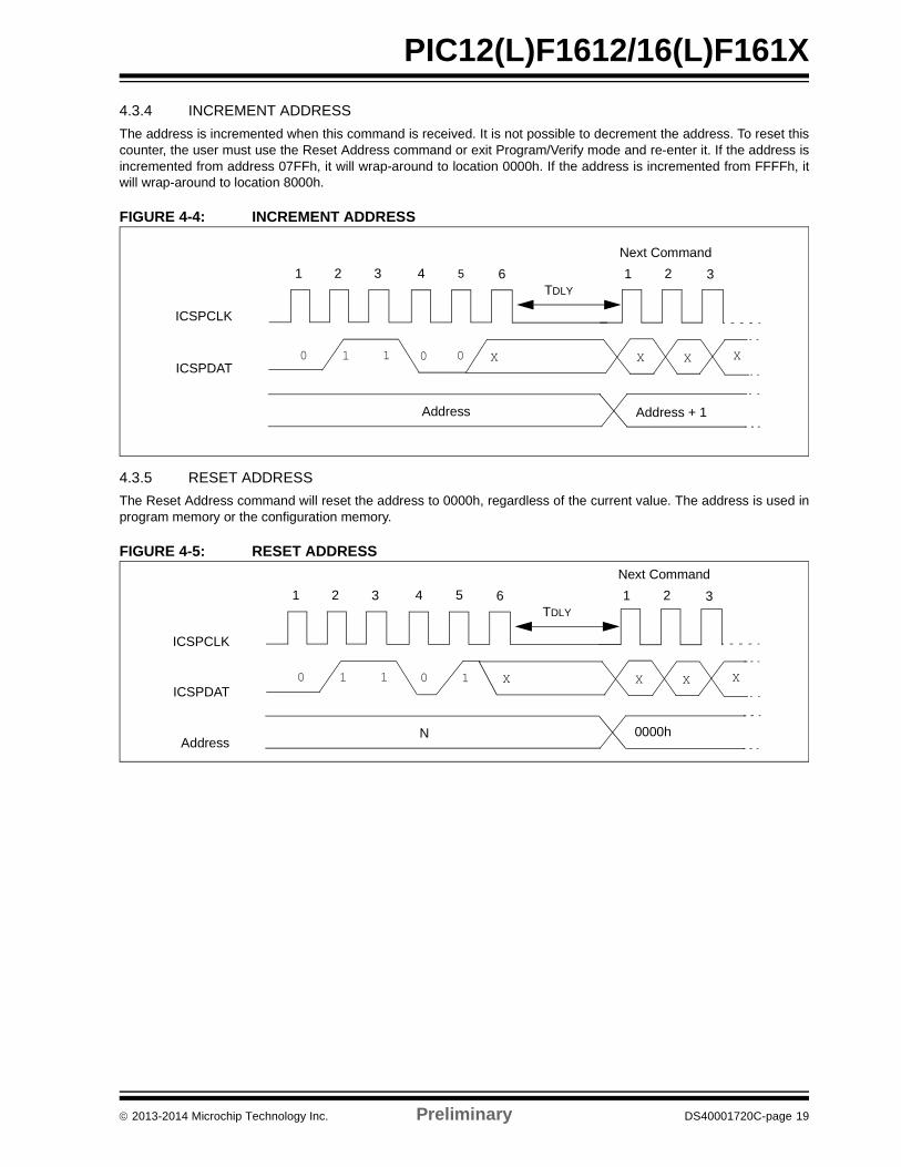
4.3.4 INCREMENT ADDRESS
The address is incremented when this command is received. It is not possible to decrement the address. To reset thiscounter, the user must use the Reset Address command or exit Program/Verify mode and re-enter it. If the address isincremented from address 07FFh, it will wrap-around to location 0000h. If the address is incremented from FFFFh, itwill wrap-around to location 8000h.
FIGURE 4-4: INCREMENT ADDRESS
4.3.5 RESET ADDRESS
The Reset Address command will reset the address to 0000h, regardless of the current value. The address is used inprogram memory or the configuration memory.
FIGURE 4-5: RESET ADDRESS
X0
1 2 3 4 5 6 1 2
ICSPCLK
ICSPDAT0 1 1
3
X X X
TDLY
Next Command
0
Address + 1Address
X0
1 2 3 4 5 6 1 2
ICSPCLK
ICSPDAT0 1 1
3
X X X
TDLY
Next Command
1
0000hNAddress
2013-2014 Microchip Technology Inc. Preliminary DS40001720C-page 19
PIC12(L)F1612/16(L)F161X
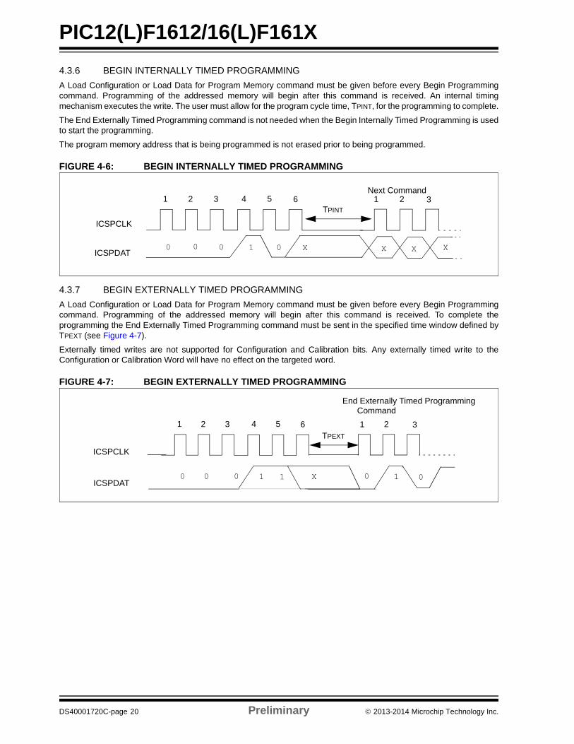
4.3.6 BEGIN INTERNALLY TIMED PROGRAMMING
A Load Configuration or Load Data for Program Memory command must be given before every Begin Programmingcommand. Programming of the addressed memory will begin after this command is received. An internal timingmechanism executes the write. The user must allow for the program cycle time, TPINT, for the programming to complete.
The End Externally Timed Programming command is not needed when the Begin Internally Timed Programming is usedto start the programming.
The program memory address that is being programmed is not erased prior to being programmed.
FIGURE 4-6: BEGIN INTERNALLY TIMED PROGRAMMING
4.3.7 BEGIN EXTERNALLY TIMED PROGRAMMING
A Load Configuration or Load Data for Program Memory command must be given before every Begin Programmingcommand. Programming of the addressed memory will begin after this command is received. To complete theprogramming the End Externally Timed Programming command must be sent in the specified time window defined byTPEXT (see Figure 4-7).
Externally timed writes are not supported for Configuration and Calibration bits. Any externally timed write to theConfiguration or Calibration Word will have no effect on the targeted word.
FIGURE 4-7: BEGIN EXTERNALLY TIMED PROGRAMMING
1 2 3 4 5 6 1 2
ICSPCLK
ICSPDAT
3TPINT
X10 0 0 X X X0
Next Command
X1 0
1 2 3 4 5 6 1 2
ICSPCLK
ICSPDAT0 0 0 1 1 0
End Externally Timed Programming Command
TPEXT
3
DS40001720C-page 20 Preliminary 2013-2014 Microchip Technology Inc.
PIC12(L)F1612/16(L)F161X
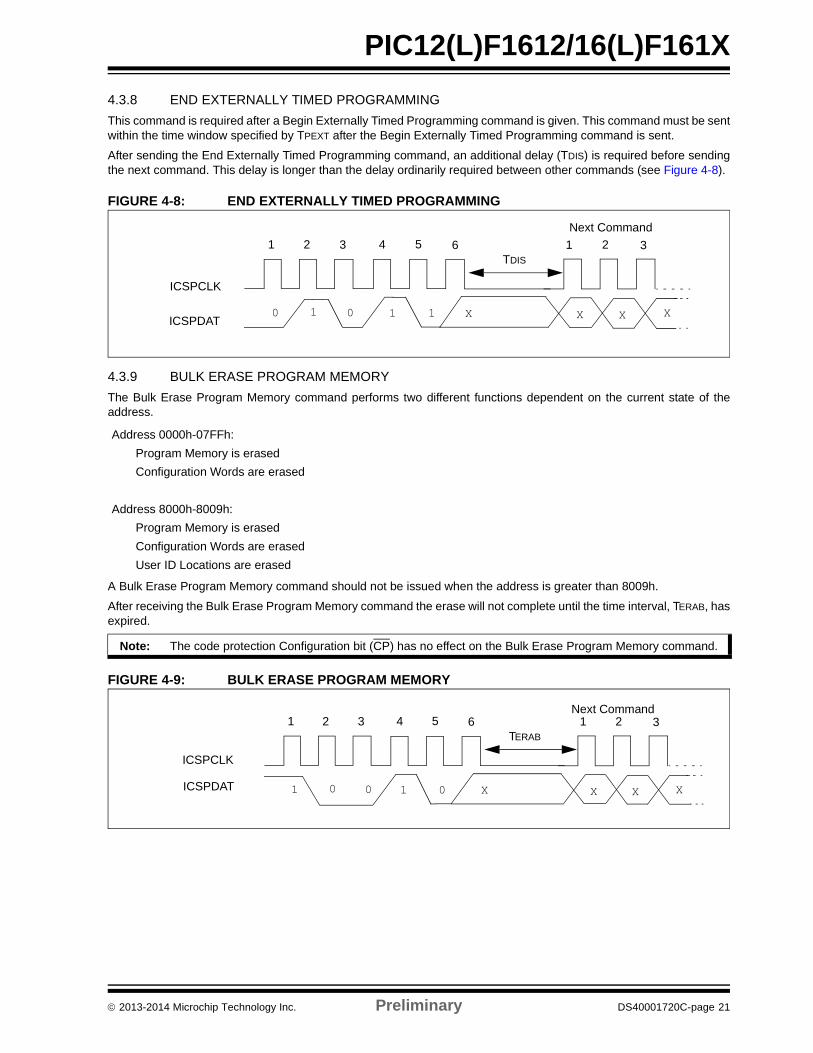
4.3.8 END EXTERNALLY TIMED PROGRAMMING
This command is required after a Begin Externally Timed Programming command is given. This command must be sentwithin the time window specified by TPEXT after the Begin Externally Timed Programming command is sent.
After sending the End Externally Timed Programming command, an additional delay (TDIS) is required before sendingthe next command. This delay is longer than the delay ordinarily required between other commands (see Figure 4-8).
FIGURE 4-8: END EXTERNALLY TIMED PROGRAMMING
4.3.9 BULK ERASE PROGRAM MEMORY
The Bulk Erase Program Memory command performs two different functions dependent on the current state of theaddress.
A Bulk Erase Program Memory command should not be issued when the address is greater than 8009h.
After receiving the Bulk Erase Program Memory command the erase will not complete until the time interval, TERAB, hasexpired.
FIGURE 4-9: BULK ERASE PROGRAM MEMORY
Address 0000h-07FFh:
Program Memory is erased
Configuration Words are erased
Address 8000h-8009h:
Program Memory is erased
Configuration Words are erased
User ID Locations are erased
Note: The code protection Configuration bit (CP) has no effect on the Bulk Erase Program Memory command.
1 2 3 4 5 6 1 2
ICSPCLK
ICSPDAT
3TDIS
X10 1 0 X X X1
Next Command
1 2 3 4 5 6 1 2
ICSPCLK
ICSPDAT
3TERAB
X11 0 0 X X X0
Next Command
2013-2014 Microchip Technology Inc. Preliminary DS40001720C-page 21
PIC12(L)F1612/16(L)F161X
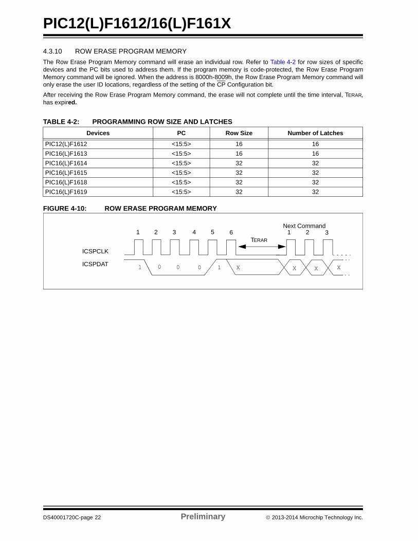
4.3.10 ROW ERASE PROGRAM MEMORY
The Row Erase Program Memory command will erase an individual row. Refer to Table 4-2 for row sizes of specificdevices and the PC bits used to address them. If the program memory is code-protected, the Row Erase ProgramMemory command will be ignored. When the address is 8000h-8009h, the Row Erase Program Memory command willonly erase the user ID locations, regardless of the setting of the CP Configuration bit.
After receiving the Row Erase Program Memory command, the erase will not complete until the time interval, TERAR,has expired.
FIGURE 4-10: ROW ERASE PROGRAM MEMORY
TABLE 4-2: PROGRAMMING ROW SIZE AND LATCHES
Devices PC Row Size Number of Latches
PIC12(L)F1612 <15:5> 16 16
PIC16(L)F1613 <15:5> 16 16
PIC16(L)F1614 <15:5> 32 32
PIC16(L)F1615 <15:5> 32 32
PIC16(L)F1618 <15:5> 32 32
PIC16(L)F1619 <15:5> 32 32
1 2 3 4 5 6 1 2
ICSPCLK
ICSPDAT
3TERAR
X01 0 0 X X X1
Next Command
DS40001720C-page 22 Preliminary 2013-2014 Microchip Technology Inc.
PIC12(L)F1612/16(L)F161X
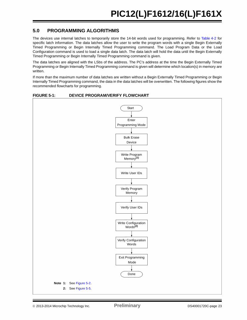
5.0 PROGRAMMING ALGORITHMS
The devices use internal latches to temporarily store the 14-bit words used for programming. Refer to Table 4-2 forspecific latch information. The data latches allow the user to write the program words with a single Begin ExternallyTimed Programming or Begin Internally Timed Programming command. The Load Program Data or the LoadConfiguration command is used to load a single data latch. The data latch will hold the data until the Begin ExternallyTimed Programming or Begin Internally Timed Programming command is given.
The data latches are aligned with the LSbs of the address. The PC’s address at the time the Begin Externally TimedProgramming or Begin Internally Timed Programming command is given will determine which location(s) in memory arewritten.
If more than the maximum number of data latches are written without a Begin Externally Timed Programming or BeginInternally Timed Programming command, the data in the data latches will be overwritten. The following figures show therecommended flowcharts for programming.
FIGURE 5-1: DEVICE PROGRAM/VERIFY FLOWCHART
Done
Start
Bulk Erase
Device
Write User IDs
Enter
Programming Mode
Write Program Memory(1)
Verify User IDs
Write Configuration Words(2)
Verify Configuration Words
Exit Programming
Mode
Verify Program Memory
Note 1: See Figure 5-2.
2: See Figure 5-5.
2013-2014 Microchip Technology Inc. Preliminary DS40001720C-page 23
PIC12(L)F1612/16(L)F161X
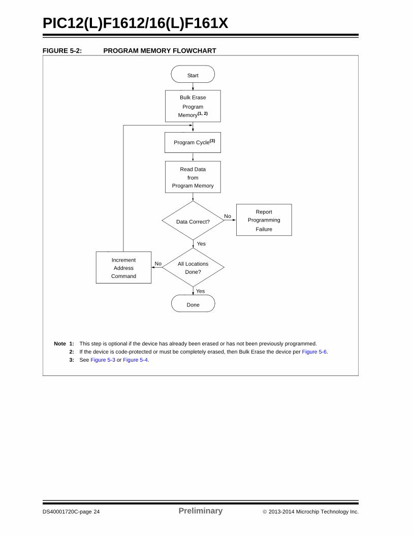
FIGURE 5-2: PROGRAM MEMORY FLOWCHART
Start
Read Data
Program Memory
Data Correct?
Report
Programming
Failure
All Locations
Done?
No
NoIncrement
Address
Command
from
Bulk Erase
Program
Yes
Memory(1, 2)
Done
Yes
Note 1: This step is optional if the device has already been erased or has not been previously programmed.
2: If the device is code-protected or must be completely erased, then Bulk Erase the device per Figure 5-6.
3: See Figure 5-3 or Figure 5-4.
Program Cycle(3)
DS40001720C-page 24 Preliminary 2013-2014 Microchip Technology Inc.
PIC12(L)F1612/16(L)F161X
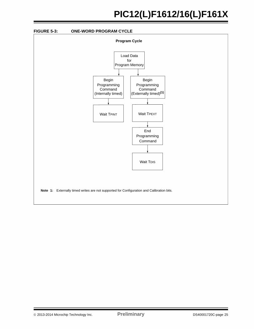
FIGURE 5-3: ONE-WORD PROGRAM CYCLE
BeginProgramming
Wait TDIS
Load Datafor
Program Memory
Command(Internally timed)
BeginProgramming
Wait TPEXT
Command(Externally timed)(1)
EndProgramming
Wait TPINT
Program Cycle
Command
Note 1: Externally timed writes are not supported for Configuration and Calibration bits.
2013-2014 Microchip Technology Inc. Preliminary DS40001720C-page 25
PIC12(L)F1612/16(L)F161X
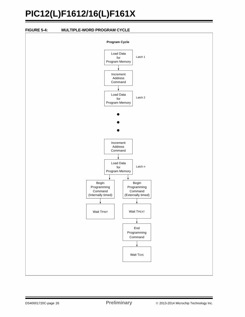
FIGURE 5-4: MULTIPLE-WORD PROGRAM CYCLE
BeginProgramming
Wait TPINT
Load Datafor
Program Memory
Command(Internally timed)
Wait TPEXT
EndProgramming
Wait TDIS
Load Datafor
Program Memory
IncrementAddress
Command
Load Datafor
Program Memory
BeginProgramming
Command(Externally timed)
Latch 1
Latch 2
Latch n
IncrementAddress
Command
Program Cycle
Command
DS40001720C-page 26 Preliminary 2013-2014 Microchip Technology Inc.
PIC12(L)F1612/16(L)F161X
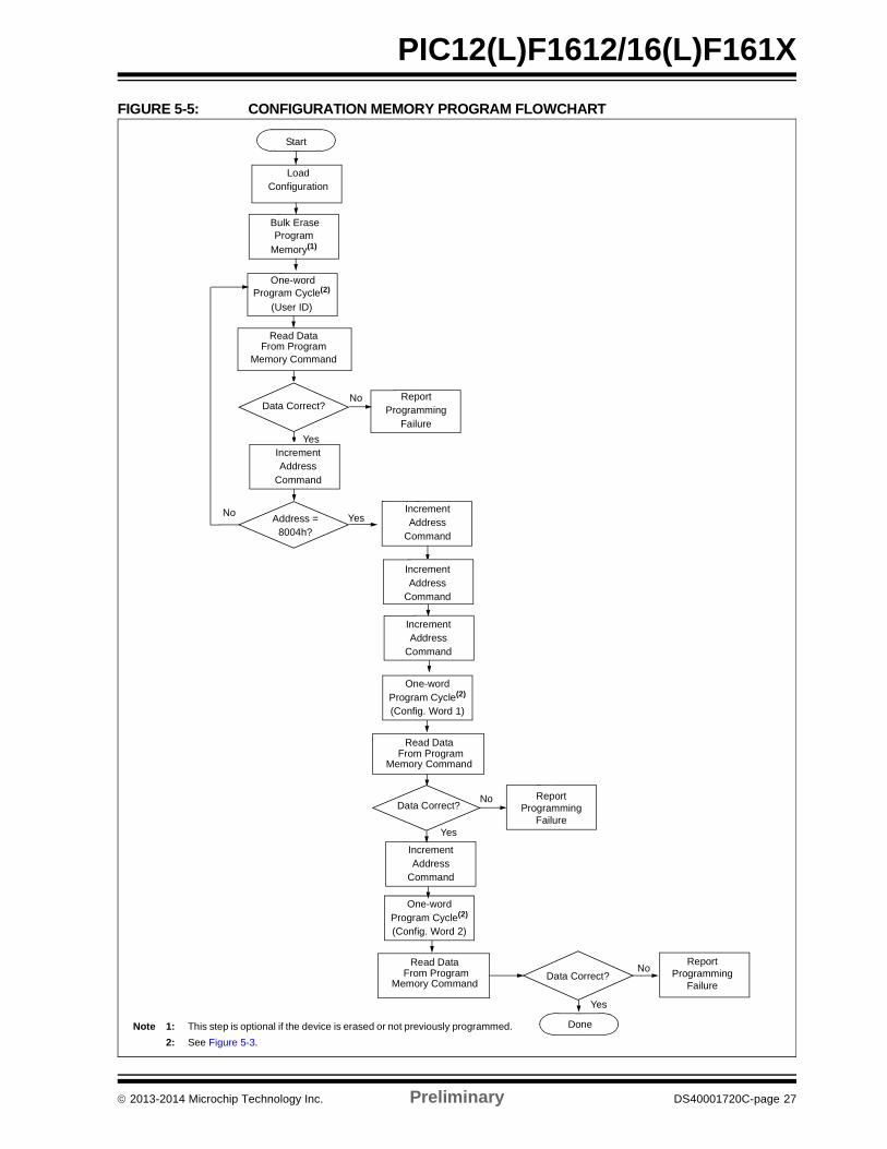
FIGURE 5-5: CONFIGURATION MEMORY PROGRAM FLOWCHART
Start
LoadConfiguration
Program Cycle(2)
Read Data
Memory Command
Data Correct?Report
ProgrammingFailure
Address =8004h?
Data Correct?Report
ProgrammingFailure
Yes
No
Yes
Yes
No
IncrementAddress
Command
No IncrementAddress
Command
Done
One-word
One-wordProgram Cycle(2)
(Config. Word 1)
IncrementAddress
Command
IncrementAddress
Command
(User ID)
From Program
Read Data
Memory CommandFrom Program
ProgramBulk Erase
Memory(1)
Data Correct?
ReportProgramming
Failure
Yes
No
One-wordProgram Cycle(2)
(Config. Word 2)
IncrementAddress
Command
Read Data
Memory CommandFrom Program
Note 1: This step is optional if the device is erased or not previously programmed.
2: See Figure 5-3.
2013-2014 Microchip Technology Inc. Preliminary DS40001720C-page 27
PIC12(L)F1612/16(L)F161X
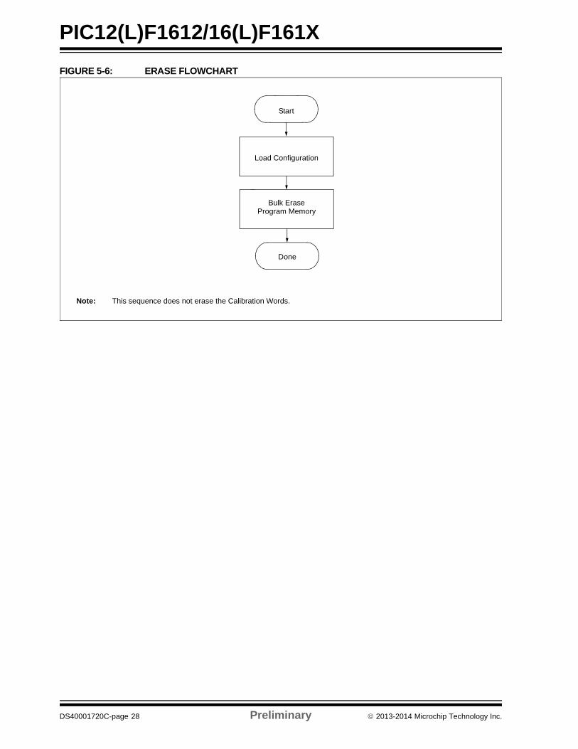
FIGURE 5-6: ERASE FLOWCHART
Start
Load Configuration
Done
Bulk EraseProgram Memory
Note: This sequence does not erase the Calibration Words.
DS40001720C-page 28 Preliminary 2013-2014 Microchip Technology Inc.
PIC12(L)F1612/16(L)F161X
6.0 CODE PROTECTION
Code protection is controlled using the CP bit in Configuration Word 1. When code protection is enabled, all programmemory locations (0000h-07FFh) read as ‘0’. Further programming is disabled for the program memory (0000h-07FFh).
The user ID locations and Configuration Words can be programmed and read out regardless of the code protectionsettings.
6.1 Program Memory
Code protection is enabled by programming the CP bit in Configuration Word 1 register to ‘0’.
The only way to disable code protection is to use the Bulk Erase Program Memory command.
7.0 HEX FILE USAGE
In the hex file there are two bytes per program word stored in the Intel® INHX32 hex format. Data is stored LSB first,MSB second. Because there are two bytes per word, the addresses in the hex file are 2x the address in programmemory. (Example: Configuration Word 1 is stored at 8007h. In the hex file this will be referenced as 1000Eh-1000Fh).
7.1 Configuration Word
To allow portability of code, it is strongly recommended that the programmer is able to read the Configuration Wordsand user ID locations from the hex file. If the Configuration Words information was not present in the hex file, a simplewarning message may be issued. Similarly, while saving a hex file, Configuration Words and user ID information shouldbe included.
7.2 Device ID
If a device ID is present in the hex file at 1000Ch-1000Dh (8006h on the part), the programmer should verify the deviceID against the value read from the part. On a mismatch condition the programmer should generate a warning message.
2013-2014 Microchip Technology Inc. Preliminary DS40001720C-page 29
PIC12(L)F1612/16(L)F161X
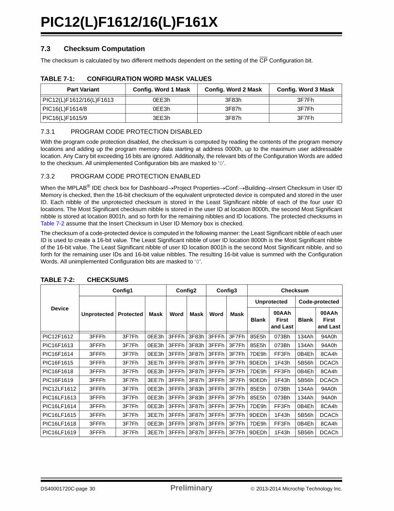
7.3 Checksum Computation
The checksum is calculated by two different methods dependent on the setting of the CP Configuration bit.
7.3.1 PROGRAM CODE PROTECTION DISABLED
With the program code protection disabled, the checksum is computed by reading the contents of the program memorylocations and adding up the program memory data starting at address 0000h, up to the maximum user addressablelocation. Any Carry bit exceeding 16 bits are ignored. Additionally, the relevant bits of the Configuration Words are addedto the checksum. All unimplemented Configuration bits are masked to ‘0’.
7.3.2 PROGRAM CODE PROTECTION ENABLED
When the MPLAB® IDE check box for DashboardProject PropertiesConf:BuildingInsert Checksum in User IDMemory is checked, then the 16-bit checksum of the equivalent unprotected device is computed and stored in the userID. Each nibble of the unprotected checksum is stored in the Least Significant nibble of each of the four user IDlocations. The Most Significant checksum nibble is stored in the user ID at location 8000h, the second Most Significantnibble is stored at location 8001h, and so forth for the remaining nibbles and ID locations. The protected checksums inTable 7-2 assume that the Insert Checksum in User ID Memory box is checked.
The checksum of a code-protected device is computed in the following manner: the Least Significant nibble of each userID is used to create a 16-bit value. The Least Significant nibble of user ID location 8000h is the Most Significant nibbleof the 16-bit value. The Least Significant nibble of user ID location 8001h is the second Most Significant nibble, and soforth for the remaining user IDs and 16-bit value nibbles. The resulting 16-bit value is summed with the ConfigurationWords. All unimplemented Configuration bits are masked to ‘0’.
TABLE 7-1: CONFIGURATION WORD MASK VALUES
Part Variant Config. Word 1 Mask Config. Word 2 Mask Config. Word 3 Mask
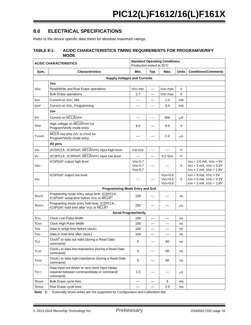
TDISTime delay from program to compare (HV discharge time)
300 — — s
TEXIT Time delay when exiting Program/Verify mode 1 — — s
TABLE 8-1: AC/DC CHARACTERISTICS TIMING REQUIREMENTS FOR PROGRAM/VERIFY MODE (CONTINUED)
AC/DC CHARACTERISTICSStandard Operating ConditionsProduction tested at 25°C
Sym. Characteristics Min. Typ. Max. Units Conditions/Comments
Note 1: Externally timed writes are not supported for Configuration and Calibration bits.
VPP
TENTH
VDD
TENTS
ICSPDAT
ICSPCLK
VIHH
VIL
TENTH
ICSPDAT
ICSPCLK
VDD
TENTS
VPP
VIHH
VIL
DS40001720C-page 32 Preliminary 2013-2014 Microchip Technology Inc.
PIC12(L)F1612/16(L)F161X
FIGURE 8-3: PROGRAMMING MODE EXIT – VPP LAST
FIGURE 8-4: PROGRAMMING MODE EXIT – VDD LAST
TEXIT
VPP
VDD
ICSPDAT
ICSPCLK
VIHH
VIL
TEXIT
VPP
VDD
ICSPDAT
ICSPCLK
VIHH
VIL
2013-2014 Microchip Technology Inc. Preliminary DS40001720C-page 33
PIC12(L)F1612/16(L)F161X
FIGURE 8-5: CLOCK AND DATA TIMING
FIGURE 8-6: WRITE COMMAND-PAYLOAD TIMING
FIGURE 8-7: READ COMMAND-PAYLOAD TIMING
as
ICSPCLK
TCKH TCKL
TDHTDS
ICSPDAT
output
TCO
ICSPDAT
ICSPDAT
ICSPDAT
TLZD
THZD
input
as
from input
from output to input
to output
1 2 3 4 5 6 1 2 15 16
X 0 LSb MSb 0
TDLY
CommandNextCommand
Payload
ICSPCLK
ICSPDATX X X X X
1 2 3 4 5 6 1 2 15 16
X
TDLY
CommandNextCommand
Payload
ICSPCLK
ICSPDATX X X X X
(from Programmer)
LSb MSb 0ICSPDAT(from Device)
x
DS40001720C-page 34 Preliminary 2013-2014 Microchip Technology Inc.
PIC12(L)F1612/16(L)F161X
FIGURE 8-8: LVP ENTRY (POWERED)
FIGURE 8-9: LVP ENTRY (POWERING UP)
TCKLTCKH
33 clocks
0 1 2 ... 31
TDH
TDS
TENTH
LSb of Pattern MSb of Pattern
VDD
MCLR
ICSPCLK
ICSPDAT
TENTS
TCKH TCKL
33 Clocks
Note 1: Sequence matching can start with no edge on MCLR first.
0 1 2 ... 31
TDH
TDS
TENTH
LSb of Pattern MSb of Pattern
VDD
MCLR
ICSPCLK
ICSPDAT
2013-2014 Microchip Technology Inc. Preliminary DS40001720C-page 35
PIC12(L)F1612/16(L)F161X
APPENDIX A: REVISION HISTORY
Revision A (09/2013)
Initial release of this document.
Revision B (04/2014)
Added PIC16(L)F1614/5/8/9 to the device family;Updated Figures 2-1 and 2-3; Added Figures 2-4through 2-7, Figure 3-2 and Figure 3-3; UpdatedRegisters 3-3 and 3-4; Updated Tables 3-1 and 4-2;Added Note to Section 4.1.3; Updated Section 7.3;Other minor corrections.
Revision C (08/2014)
Updated part number in Figure 2-2 (14-Pin PDIP, SOIC,TSSOP); Deleted Figure 2-4 (14-Pin PDIP, SOIC,TSSOP); Added Note 3 to Register 3-4; Updated Note5 in Register 3-3; Updated Tables 7-1 and 7-2; Otherminor corrections.
DS40001720C-page 36 Preliminary 2013-2014 Microchip Technology Inc.
Note the following details of the code protection feature on Microchip devices:
• Microchip products meet the specification contained in their particular Microchip Data Sheet.
• Microchip believes that its family of products is one of the most secure families of its kind on the market today, when used in the intended manner and under normal conditions.
• There are dishonest and possibly illegal methods used to breach the code protection feature. All of these methods, to our knowledge, require using the Microchip products in a manner outside the operating specifications contained in Microchip’s Data Sheets. Most likely, the person doing so is engaged in theft of intellectual property.
• Microchip is willing to work with the customer who is concerned about the integrity of their code.
• Neither Microchip nor any other semiconductor manufacturer can guarantee the security of their code. Code protection does not mean that we are guaranteeing the product as “unbreakable.”
Code protection is constantly evolving. We at Microchip are committed to continuously improving the code protection features of ourproducts. Attempts to break Microchip’s code protection feature may be a violation of the Digital Millennium Copyright Act. If such actsallow unauthorized access to your software or other copyrighted work, you may have a right to sue for relief under that Act.
Information contained in this publication regarding deviceapplications and the like is provided only for your convenienceand may be superseded by updates. It is your responsibility toensure that your application meets with your specifications.MICROCHIP MAKES NO REPRESENTATIONS ORWARRANTIES OF ANY KIND WHETHER EXPRESS ORIMPLIED, WRITTEN OR ORAL, STATUTORY OROTHERWISE, RELATED TO THE INFORMATION,INCLUDING BUT NOT LIMITED TO ITS CONDITION,QUALITY, PERFORMANCE, MERCHANTABILITY ORFITNESS FOR PURPOSE. Microchip disclaims all liabilityarising from this information and its use. Use of Microchipdevices in life support and/or safety applications is entirely atthe buyer’s risk, and the buyer agrees to defend, indemnify andhold harmless Microchip from any and all damages, claims,suits, or expenses resulting from such use. No licenses areconveyed, implicitly or otherwise, under any Microchipintellectual property rights.
2013-2014 Microchip Technology Inc. Prelimin
QUALITY MANAGEMENT SYSTEM CERTIFIED BY DNV
== ISO/TS 16949 ==
Trademarks
The Microchip name and logo, the Microchip logo, dsPIC, FlashFlex, flexPWR, JukeBlox, KEELOQ, KEELOQ logo, Kleer, LANCheck, MediaLB, MOST, MOST logo, MPLAB, OptoLyzer, PIC, PICSTART, PIC32 logo, RightTouch, SpyNIC, SST, SST Logo, SuperFlash and UNI/O are registered trademarks of Microchip Technology Incorporated in the U.S.A. and other countries.
The Embedded Control Solutions Company and mTouch are registered trademarks of Microchip Technology Incorporated in the U.S.A.
Analog-for-the-Digital Age, BodyCom, chipKIT, chipKIT logo, CodeGuard, dsPICDEM, dsPICDEM.net, ECAN, In-Circuit Serial Programming, ICSP, Inter-Chip Connectivity, KleerNet, KleerNet logo, MiWi, MPASM, MPF, MPLAB Certified logo, MPLIB, MPLINK, MultiTRAK, NetDetach, Omniscient Code Generation, PICDEM, PICDEM.net, PICkit, PICtail, RightTouch logo, REAL ICE, SQI, Serial Quad I/O, Total Endurance, TSHARC, USBCheck, VariSense, ViewSpan, WiperLock, Wireless DNA, and ZENA are trademarks of Microchip Technology Incorporated in the U.S.A. and other countries.
SQTP is a service mark of Microchip Technology Incorporated in the U.S.A.
Silicon Storage Technology is a registered trademark of Microchip Technology Inc. in other countries.
GestIC is a registered trademarks of Microchip Technology Germany II GmbH & Co. KG, a subsidiary of Microchip Technology Inc., in other countries.
All other trademarks mentioned herein are property of their respective companies.
Microchip received ISO/TS-16949:2009 certification for its worldwide
ary DS400001720C-page 37
headquarters, design and wafer fabrication facilities in Chandler and Tempe, Arizona; Gresham, Oregon and design centers in California and India. The Company’s quality system processes and procedures are for its PIC® MCUs and dsPIC® DSCs, KEELOQ® code hopping devices, Serial EEPROMs, microperipherals, nonvolatile memory and analog products. In addition, Microchip’s quality system for the design and manufacture of development systems is ISO 9001:2000 certified.
DS40001720C-page 38 Preliminary 2013-2014 Microchip Technology Inc.
AMERICASCorporate Office2355 West Chandler Blvd.Chandler, AZ 85224-6199Tel: 480-792-7200 Fax: 480-792-7277Technical Support: http://www.microchip.com/supportWeb Address: www.microchip.com
AtlantaDuluth, GA Tel: 678-957-9614 Fax: 678-957-1455
Austin, TXTel: 512-257-3370
BostonWestborough, MA Tel: 774-760-0087 Fax: 774-760-0088
ChicagoItasca, IL Tel: 630-285-0071 Fax: 630-285-0075