176
2004 Microchip Technology Inc. DS39598E PIC16F818/819 Data Sheet 18/20-Pin Enhanced Flash Microcontrollers with nanoWatt Technology

2004 Microchip Technology Inc. DS39598E
PIC16F818/819Data Sheet
18/20-PinEnhanced Flash Microcontrollers
with nanoWatt Technology

Note the following details of the code protection feature on Microchip devices:
• Microchip products meet the specification contained in their particular Microchip Data Sheet.
• Microchip believes that its family of products is one of the most secure families of its kind on the market today, when used in the intended manner and under normal conditions.
• There are dishonest and possibly illegal methods used to breach the code protection feature. All of these methods, to our knowledge, require using the Microchip products in a manner outside the operating specifications contained in Microchip’s Data Sheets. Most likely, the person doing so is engaged in theft of intellectual property.
• Microchip is willing to work with the customer who is concerned about the integrity of their code.
• Neither Microchip nor any other semiconductor manufacturer can guarantee the security of their code. Code protection does not mean that we are guaranteeing the product as “unbreakable.”
Code protection is constantly evolving. We at Microchip are committed to continuously improving the code protection features of ourproducts. Attempts to break Microchip’s code protection feature may be a violation of the Digital Millennium Copyright Act. If such actsallow unauthorized access to your software or other copyrighted work, you may have a right to sue for relief under that Act.
Information contained in this publication regarding deviceapplications and the like is provided only for your convenienceand may be superseded by updates. It is your responsibility toensure that your application meets with your specifications.MICROCHIP MAKES NO REPRESENTATIONS OR WAR-RANTIES OF ANY KIND WHETHER EXPRESS OR IMPLIED,WRITTEN OR ORAL, STATUTORY OR OTHERWISE,RELATED TO THE INFORMATION, INCLUDING BUT NOTLIMITED TO ITS CONDITION, QUALITY, PERFORMANCE,MERCHANTABILITY OR FITNESS FOR PURPOSE.Microchip disclaims all liability arising from this information andits use. Use of Microchip’s products as critical components inlife support systems is not authorized except with expresswritten approval by Microchip. No licenses are conveyed,implicitly or otherwise, under any Microchip intellectual propertyrights.
DS39598E-page ii
Trademarks
The Microchip name and logo, the Microchip logo, Accuron, dsPIC, KEELOQ, microID, MPLAB, PIC, PICmicro, PICSTART, PRO MATE, PowerSmart, rfPIC, and SmartShunt are registered trademarks of Microchip Technology Incorporated in the U.S.A. and other countries.
AmpLab, FilterLab, MXDEV, MXLAB, PICMASTER, SEEVAL, SmartSensor and The Embedded Control Solutions Company are registered trademarks of Microchip Technology Incorporated in the U.S.A.
Analog-for-the-Digital Age, Application Maestro, dsPICDEM, dsPICDEM.net, dsPICworks, ECAN, ECONOMONITOR, FanSense, FlexROM, fuzzyLAB, In-Circuit Serial Programming, ICSP, ICEPIC, Migratable Memory, MPASM, MPLIB, MPLINK, MPSIM, PICkit, PICDEM, PICDEM.net, PICLAB, PICtail, PowerCal, PowerInfo, PowerMate, PowerTool, rfLAB, rfPICDEM, Select Mode, Smart Serial, SmartTel and Total Endurance are trademarks of Microchip Technology Incorporated in the U.S.A. and other countries.
SQTP is a service mark of Microchip Technology Incorporated in the U.S.A.
All other trademarks mentioned herein are property of their respective companies.
© 2004, Microchip Technology Incorporated, Printed in the U.S.A., All Rights Reserved.
Printed on recycled paper.
2004 Microchip Technology Inc.
Microchip received ISO/TS-16949:2002 quality system certification for its worldwide headquarters, design and wafer fabrication facilities in Chandler and Tempe, Arizona and Mountain View, California in October 2003. The Company’s quality system processes and procedures are for its PICmicro® 8-bit MCUs, KEELOQ® code hopping devices, Serial EEPROMs, microperipherals, nonvolatile memory and analog products. In addition, Microchip’s quality system for the design and manufacture of development systems is ISO 9001:2000 certified.

PIC16F818/81918/20-Pin Enhanced Flash Microcontrollers
with nanoWatt Technology
Low-Power Features: • Power-Managed modes:
- Primary Run: XT, RC oscillator, 87 µA, 1 MHz, 2V
- INTRC: 7 µA, 31.25 kHz, 2V- Sleep: 0.2 µA, 2V
• Timer1 oscillator: 1.8 µA, 32 kHz, 2V
• Watchdog Timer: 0.7 µA, 2V• Wide operating voltage range:
- Industrial: 2.0V to 5.5V
Oscillators:• Three Crystal modes:
- LP, XT, HS: up to 20 MHz
• Two External RC modes• One External Clock mode:
- ECIO: up to 20 MHz
• Internal oscillator block:- 8 user selectable frequencies: 31 kHz, 125 kHz,
250 kHz, 500 kHz, 1 MHz, 2 MHz, 4 MHz, 8 MHz
Peripheral Features:• 16 I/O pins with individual direction control
• High sink/source current: 25 mA• Timer0: 8-bit timer/counter with 8-bit prescaler• Timer1: 16-bit timer/counter with prescaler, can be
incremented during Sleep via external crystal/clock• Timer2: 8-bit timer/counter with 8-bit period
register, prescaler and postscaler • Capture, Compare, PWM (CCP) module:
- Capture is 16-bit, max. resolution is 12.5 ns- Compare is 16-bit, max. resolution is 200 ns- PWM max. resolution is 10-bit
• 10-bit, 5-channel Analog-to-Digital converter• Synchronous Serial Port (SSP) with
SPI™ (Master/Slave) and I2C™ (Slave)
Pin Diagram
Special Microcontroller Features:• 100,000 erase/write cycles Enhanced Flash
program memory typical• 1,000,000 typical erase/write cycles EEPROM
data memory typical• EEPROM Data Retention: > 40 years
• In-Circuit Serial ProgrammingTM (ICSPTM) via two pins• Processor read/write access to program memory• Low-Voltage Programming
• In-Circuit Debugging via two pins
RA1/AN1RA0/AN0RA7/OSC1/CLKIRA6/OSC2/CLKOVDD
RB7/T1OSI/PGDRB6/T1OSO/T1CKI/PGCRB5/SSRB4/SCK/SCL
RA2/AN2/VREF-RA3/AN3/VREF+RA4/AN4/T0CKIRA5/MCLR/VPP
VSS
RB0/INTRB1/SDI/SDA
RB2/SDO/CCP1RB3/CCP1/PGM
•123456789
181716151413121110
PIC
16F
818/
819
18-Pin PDIP, SOIC
Device
Program Memory Data Memory
I/O Pins10-bit
A/D (ch)CCP
(PWM)
SSPTimers8/16-bitFlash
(Bytes)# Single-Word Instructions
SRAM (Bytes)
EEPROM (Bytes)
SPI™Slave I2C™
PIC16F818 1792 1024 128 128 16 5 1 Y Y 2/1
PIC16F819 3584 2048 256 256 16 5 1 Y Y 2/1
2004 Microchip Technology Inc. DS39598E-page 1

PIC16F818/819
Pin Diagrams
RA1/AN1RA0/AN0RA7/OSC1/CLKIRA6/OSC2/CLKOVDDRB7/T1OSI/PGDRB6/T1OSO/T1CKI/PGCRB5/SSRB4/SCK/SCL
RA2/AN2/VREF-RA3/AN3/VREF+RA4/AN4/T0CKIRA5/MCLR/VPP
VSSRB0/INT
RB1/SDI/SDARB2/SDO/CCP1RB3/CCP1/PGM
•123456789
181716151413121110
18-Pin PDIP, SOIC
PIC
16F
818/
819
RA1/AN1RA0/AN0RA7/OSC1/CLKIRA6/OSC2/CLKOVDD
RB7/T1OSI/PGDRB6/T1OSO/T1CKI/PGCRB5/SSRB4/SCK/SCL
RA2/AN2/VREF-RA3/AN3/VREF+RA4/AN4/T0CKIRA5/MCLR/VPP
VSS
RB0/INTRB1/SDI/SDA
RB2/SDO/CCP1RB3/CCP1/PGM
•123456789
201918171615141312
20-Pin SSOP
10 11
VSS
VDD
PIC
16F
818/
819
28-Pin QFN
16
2
RA
2/A
N2/
VR
EF-
RA
0/A
N0
RA
4/A
N4/
T0C
KI
RA5/MCLR/VPP
NC
VSS
NC
RB0/INT
RB
1/S
DI/S
DA
RA
3/A
N3/
VR
EF+
RA7/OSC1/CLKI
RA6/OSC2/CLKO
VDD
NC
VDD
RB7/T1OSI/PGD
RB6/T1OSO/T1CKI/PGC
RB
5/S
S
RB
4/S
CK
/SC
L
7
PIC16F818/819
1
3
6
5
4
15
21
19
20
17
18
2228 2627 232425
148 109 131211
VSS
NC
NC
RA
1/A
N1
RB
2/S
DO
/CC
P1
RB
3/C
CP
1/P
GM
NC
NC
NC
DS39598E-page 2 2004 Microchip Technology Inc.

PIC16F818/819
Table of Contents
1.0 Device Overview .......................................................................................................................................................................... 52.0 Memory Organization ................................................................................................................................................................... 93.0 Data EEPROM and Flash Program Memory.............................................................................................................................. 254.0 Oscillator Configurations ............................................................................................................................................................ 335.0 I/O Ports ..................................................................................................................................................................................... 396.0 Timer0 Module ........................................................................................................................................................................... 537.0 Timer1 Module ........................................................................................................................................................................... 578.0 Timer2 Module ........................................................................................................................................................................... 639.0 Capture/Compare/PWM (CCP) Module ..................................................................................................................................... 6510.0 Synchronous Serial Port (SSP) Module ..................................................................................................................................... 7111.0 Analog-to-Digital Converter (A/D) Module.................................................................................................................................. 8112.0 Special Features of the CPU...................................................................................................................................................... 8913.0 Instruction Set Summary .......................................................................................................................................................... 10314.0 Development Support............................................................................................................................................................... 11115.0 Electrical Characteristics .......................................................................................................................................................... 11716.0 DC and AC Characteristics Graphs and Tables....................................................................................................................... 14317.0 Packaging Information.............................................................................................................................................................. 157Appendix A: Revision History............................................................................................................................................................. 163Appendix B: Device Differences ........................................................................................................................................................ 163Index .................................................................................................................................................................................................. 165On-Line Support................................................................................................................................................................................. 171Systems Information and Upgrade Hot Line ...................................................................................................................................... 171Reader Response .............................................................................................................................................................................. 172PIC16F818/819 Product Identification System .................................................................................................................................. 173
TO OUR VALUED CUSTOMERS
It is our intention to provide our valued customers with the best documentation possible to ensure successful use of your Microchipproducts. To this end, we will continue to improve our publications to better suit your needs. Our publications will be refined andenhanced as new volumes and updates are introduced.
If you have any questions or comments regarding this publication, please contact the Marketing Communications Department viaE-mail at [email protected] or fax the Reader Response Form in the back of this data sheet to (480) 792-4150. Wewelcome your feedback.
Most Current Data SheetTo obtain the most up-to-date version of this data sheet, please register at our Worldwide Web site at:
http://www.microchip.com
You can determine the version of a data sheet by examining its literature number found on the bottom outside corner of any page.The last character of the literature number is the version number, (e.g., DS30000A is version A of document DS30000).
ErrataAn errata sheet, describing minor operational differences from the data sheet and recommended workarounds, may exist for currentdevices. As device/documentation issues become known to us, we will publish an errata sheet. The errata will specify the revisionof silicon and revision of document to which it applies.
To determine if an errata sheet exists for a particular device, please check with one of the following:
• Microchip’s Worldwide Web site; http://www.microchip.com• Your local Microchip sales office (see last page)When contacting a sales office, please specify which device, revision of silicon and data sheet (include literature number) you areusing.
Customer Notification SystemRegister on our web site at www.microchip.com to receive the most current information on all of our products.
2004 Microchip Technology Inc. DS39598E-page 3

PIC16F818/819
NOTES:
DS39598E-page 4 2004 Microchip Technology Inc.

PIC16F818/819
1.0 DEVICE OVERVIEW
This document contains device specific information forthe operation of the PIC16F818/819 devices. Additionalinformation may be found in the “PICmicro® Mid-RangeMCU Family Reference Manual” (DS33023) which maybe downloaded from the Microchip web site. TheReference Manual should be considered a complemen-tary document to this data sheet and is highlyrecommended reading for a better understanding of thedevice architecture and operation of the peripheralmodules.
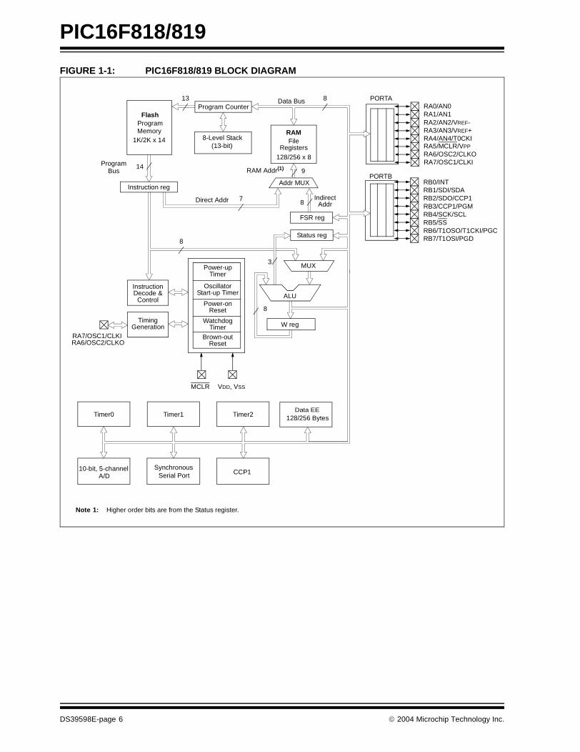
The PIC16F818/819 belongs to the Mid-Range familyof the PICmicro® devices. The devices differ from eachother in the amount of Flash program memory, datamemory and data EEPROM (see Table 1-1). A blockdiagram of the devices is shown in Figure 1-1. Thesedevices contain features that are new to the PIC16product line:
• Internal RC oscillator with eight selectable frequencies, including 31.25 kHz, 125 kHz, 250 kHz, 500 kHz, 1 MHz, 2 MHz, 4 MHz and 8 MHz. The INTRC can be configured as the system clock via the configuration bits. Refer to Section 4.5 “Internal Oscillator Block” and Section 12.1 “Configuration Bits” for further details.
• The Timer1 module current consumption has been greatly reduced from 20 µA (previous PIC16 devices) to 1.8 µA typical (32 kHz at 2V), which is ideal for real-time clock applications. Refer to Section 6.0 “Timer0 Module” for further details.
• The amount of oscillator selections has increased. The RC and INTRC modes can be selected with an I/O pin configured as an I/O or a clock output (FOSC/4). An external clock can be configured with an I/O pin. Refer to Section 4.0 “Oscillator Configurations” for further details.
TABLE 1-1: AVAILABLE MEMORY IN PIC16F818/819 DEVICES
There are 16 I/O pins that are user configurable on apin-to-pin basis. Some pins are multiplexed with otherdevice functions. These functions include:
• External Interrupt• Change on PORTB Interrupt
• Timer0 Clock Input• Low-Power Timer1 Clock/Oscillator• Capture/Compare/PWM
• 10-bit, 5-channel Analog-to-Digital Converter• SPI/I2C• MCLR (RA5) can be configured as an Input
Table 1-2 details the pinout of the devices withdescriptions and details for each pin.
DeviceProgram
FlashData
MemoryData
EEPROM
PIC16F818 1K x 14 128 x 8 128 x 8
PIC16F819 2K x14 256 x 8 256 x 8
2004 Microchip Technology Inc. DS39598E-page 5
PIC16F818/819
FIGURE 1-1: PIC16F818/819 BLOCK DIAGRAM
Flash
Memory1K/2K x 14
13 Data Bus 8
14ProgramBus
Instruction reg
Program Counter
8-Level Stack(13-bit)
RAMFile
Registers128/256 x 8
Direct Addr 7
RAM Addr(1) 9
Addr MUX
IndirectAddr
FSR reg
Status reg
MUX
ALU
W reg
Power-upTimer
OscillatorStart-up Timer
Power-onReset
WatchdogTimer
InstructionDecode &
Control
TimingGeneration
RA7/OSC1/CLKIRA6/OSC2/CLKO
MCLR VDD, VSS
Timer0
10-bit, 5-channel SynchronousSerial Port
PORTA
8
8
Brown-outReset
Note 1: Higher order bits are from the Status register.
CCP1
Timer1 Timer2
RA5/MCLR/VPP
RA6/OSC2/CLKO
RA4/AN4/T0CKIRA3/AN3/VREF+RA2/AN2/VREF-RA1/AN1
8
3
Program
PORTBRB0/INTRB1/SDI/SDARB2/SDO/CCP1RB3/CCP1/PGMRB4/SCK/SCLRB5/SSRB6/T1OSO/T1CKI/PGCRB7/T1OSI/PGD
RA7/OSC1/CLKI
RA0/AN0
128/256 BytesData EE
A/D
DS39598E-page 6 2004 Microchip Technology Inc.

PIC16F818/819
TABLE 1-2: PIC16F818/819 PINOUT DESCRIPTIONS
Pin NamePDIP/SOICPin#
SSOPPin#
QFNPin#
I/O/PType
BufferType
Description
PORTA is a bidirectional I/O port.
RA0/AN0RA0AN0
17 19 23I/OI
TTLAnalog
Bidirectional I/O pin.Analog input channel 0.
RA1/AN1RA1AN1
18 20 24I/OI
TTLAnalog
Bidirectional I/O pin.Analog input channel 1.
RA2/AN2/VREF-RA2AN2VREF-
1 1 26I/OII
TTLAnalogAnalog
Bidirectional I/O pin.Analog input channel 2.A/D reference voltage (low) input.
RA3/AN3/VREF+RA3AN3VREF+
2 2 27I/OII
TTLAnalogAnalog
Bidirectional I/O pin.Analog input channel 3.A/D reference voltage (high) input.
RA4/AN4/T0CKIRA4AN4T0CKI
3 3 28I/OII
STAnalog
ST
Bidirectional I/O pin.Analog input channel 4.Clock input to the TMR0 timer/counter.
RA5/MCLR/VPP
RA5MCLR
VPP
4 4 1II
P
STST
–
Input pin. Master Clear (Reset). Input/programming voltage input. This pin is an active-low Reset to the device. Programming threshold voltage.
RA6/OSC2/CLKORA6OSC2
CLKO
15 17 20I/OO
O
ST–
–
Bidirectional I/O pin. Oscillator crystal output. Connects to crystal or resonator in Crystal Oscillator mode. In RC mode, this pin outputs CLKO signal which has 1/4 the frequency of OSC1 and denotes the instruction cycle rate.
RA7/OSC1/CLKIRA7OSC1CLKI
16 18 21I/OII
STST/CMOS(3)
–
Bidirectional I/O pin.Oscillator crystal input.External clock source input.
Legend: I = Input O = Output I/O = Input/Output P = Power– = Not used TTL = TTL Input ST = Schmitt Trigger Input
Note 1: This buffer is a Schmitt Trigger input when configured as the external interrupt.
2: This buffer is a Schmitt Trigger input when used in Serial Programming mode.3: This buffer is a Schmitt Trigger input when configured in RC Oscillator mode and a CMOS input otherwise.
2004 Microchip Technology Inc. DS39598E-page 7

PIC16F818/819
PORTB is a bidirectional I/O port. PORTB can be software programmed for internal weak pull-up on all inputs.
RB0/INTRB0INT
6 7 7I/OI
TTLST(1)
Bidirectional I/O pin.External interrupt pin.
RB1/SDI/SDARB1SDISDA
7 8 8I/OI
I/O
TTLSTST
Bidirectional I/O pin.SPI™ data in.I2C™ data.
RB2/SDO/CCP1RB2SDOCCP1
8 9 9I/OO
I/O
TTLSTST
Bidirectional I/O pin.SPI data out.Capture input, Compare output, PWM output.
RB3/CCP1/PGMRB3CCP1PGM
9 10 10I/OI/OI
TTLSTST
Bidirectional I/O pin.Capture input, Compare output, PWM output.Low-Voltage ICSP™ Programming enable pin.
RB4/SCK/SCLRB4SCKSCL
10 11 12I/OI/OI
TTLSTST
Bidirectional I/O pin. Interrupt-on-change pin.Synchronous serial clock input/output for SPI.Synchronous serial clock input for I2C.
RB5/SSRB5SS
11 12 13I/OI
TTLTTL
Bidirectional I/O pin. Interrupt-on-change pin.Slave select for SPI in Slave mode.
RB6/T1OSO/T1CKI/PGCRB6T1OSOT1CKIPGC
12 13 15I/OOII
TTLSTST
ST(2)
Interrupt-on-change pin.Timer1 Oscillator output.Timer1 clock input.In-circuit debugger and ICSP programming clock pin.
RB7/T1OSI/PGDRB7T1OSIPGD
13 14 16I/OII
TTLST
ST(2)
Interrupt-on-change pin. Timer1 oscillator input.In-circuit debugger and ICSP programming data pin.
VSS 5 5, 6 3, 5 P – Ground reference for logic and I/O pins.
VDD 14 15, 16 17, 19 P – Positive supply for logic and I/O pins.
TABLE 1-2: PIC16F818/819 PINOUT DESCRIPTIONS (CONTINUED)
Pin NamePDIP/SOICPin#
SSOPPin#
QFNPin#
I/O/PType
BufferType
Description
Legend: I = Input O = Output I/O = Input/Output P = Power– = Not used TTL = TTL Input ST = Schmitt Trigger Input
Note 1: This buffer is a Schmitt Trigger input when configured as the external interrupt.2: This buffer is a Schmitt Trigger input when used in Serial Programming mode.3: This buffer is a Schmitt Trigger input when configured in RC Oscillator mode and a CMOS input otherwise.
DS39598E-page 8 2004 Microchip Technology Inc.

PIC16F818/819
2.0 MEMORY ORGANIZATION
There are two memory blocks in the PIC16F818/819.These are the program memory and the data memory.Each block has its own bus, so access to each blockcan occur during the same oscillator cycle.
The data memory can be further broken down into thegeneral purpose RAM and the Special FunctionRegisters (SFRs). The operation of the SFRs thatcontrol the “core” are described here. The SFRs usedto control the peripheral modules are described in thesection discussing each individual peripheral module.
The data memory area also contains the dataEEPROM memory. This memory is not directly mappedinto the data memory but is indirectly mapped. That is,an indirect address pointer specifies the address of thedata EEPROM memory to read/write. The PIC16F818device’s 128 bytes of data EEPROM memory have theaddress range of 00h-7Fh and the PIC16F819 device’s256 bytes of data EEPROM memory have the addressrange of 00h-FFh. More details on the EEPROMmemory can be found in Section 3.0 “Data EEPROMand Flash Program Memory”.
Additional information on device memory may be foundin the “PICmicro® Mid-Range Reference Manual”(DS33023).
FIGURE 2-1: PROGRAM MEMORY MAP AND STACK FOR PIC16F818
2.1 Program Memory Organization
The PIC16F818/819 devices have a 13-bit programcounter capable of addressing an 8K x 14 programmemory space. For the PIC16F818, the first 1K x 14(0000h-03FFh) is physically implemented (seeFigure 2-1). For the PIC16F819, the first 2K x 14 islocated at 0000h-07FFh (see Figure 2-2). Accessing alocation above the physically implemented address willcause a wraparound. For example, the same instruc-tion will be accessed at locations 020h, 420h, 820h,C20h, 1020h, 1420h, 1820h and 1C20h.
The Reset vector is at 0000h and the interrupt vector isat 0004h.
FIGURE 2-2: PROGRAM MEMORY MAP AND STACK FOR PIC16F819
PC<12:0>
13
0000h
0004h0005h
Stack Level 1
Stack Level 8
Reset Vector
Interrupt Vector
On-Chip
CALL, RETURNRETFIE, RETLW
1FFFh
Stack Level 2
ProgramMemory
Page 003FFh0400h
Wraps to0000h-03FFh
PC<12:0>
13
0000h
0004h0005h
Stack Level 1
Stack Level 8
Reset Vector
Interrupt Vector
On-Chip
CALL, RETURNRETFIE, RETLW
1FFFh
Stack Level 2
ProgramMemory Page 0
07FFh0800h
Wraps to0000h-07FFh
2004 Microchip Technology Inc. DS39598E-page 9

PIC16F818/819
2.2 Data Memory Organization
The data memory is partitioned into multiple banks thatcontain the General Purpose Registers and the SpecialFunction Registers. Bits RP1 (Status<6>) and RP0(Status<5>) are the bank select bits.
Each bank extends up to 7Fh (128 bytes). The lowerlocations of each bank are reserved for the SpecialFunction Registers. Above the Special Function Regis-ters are the General Purpose Registers, implementedas static RAM. All implemented banks contain SFRs.Some “high use” SFRs from one bank may be mirroredin another bank for code reduction and quicker access(e.g., the Status register is in Banks 0-3).
2.2.1 GENERAL PURPOSE REGISTER FILE
The register file can be accessed either directly orindirectly through the File Select Register, FSR.
RP1:RP0 Bank
00 0
01 1
10 2
11 3
Note: EEPROM data memory description can befound in Section 3.0 “Data EEPROM andFlash Program Memory” of this datasheet.
DS39598E-page 10 2004 Microchip Technology Inc.
PIC16F818/819
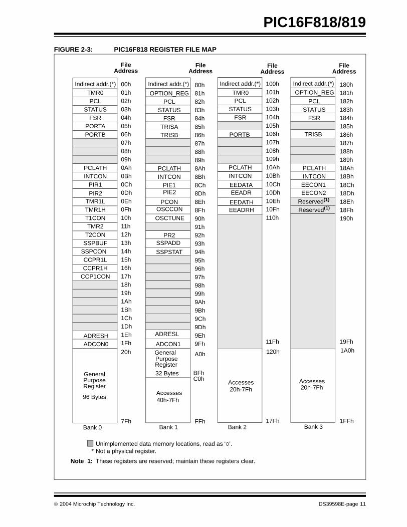
FIGURE 2-3: PIC16F818 REGISTER FILE MAP
Indirect addr.(*)
TMR0PCL
STATUSFSR
PORTAPORTB
PCLATHINTCON
PIR1
TMR1LTMR1HT1CONTMR2
T2CONSSPBUF
SSPCONCCPR1LCCPR1H
CCP1CON
OPTION_REGPCL
STATUSFSR
TRISATRISB
PCLATHINTCON
PIE1
PCON
PR2
SSPSTAT
00h01h02h03h04h05h06h07h08h09h0Ah0Bh0Ch0Dh0Eh0Fh10h11h12h13h14h15h16h17h18h19h1Ah1Bh1Ch1Dh1Eh1Fh
80h81h82h83h84h85h86h87h88h89h8Ah8Bh8Ch8Dh8Eh8Fh90h91h92h93h94h95h96h97h98h99h9Ah9Bh9Ch9Dh9Eh9Fh
20h A0h
7Fh FFhBank 0 Bank 1
FileAddress
Indirect addr.(*) Indirect addr.(*)
PCLSTATUS
FSR
PCLATHINTCON
PCLSTATUS
FSR
PCLATHINTCON
100h101h102h103h104h105h106h107h108h109h10Ah10Bh
180h181h182h183h184h185h186h187h188h189h18Ah18Bh
17Fh 1FFhBank 2 Bank 3
Indirect addr.(*)
TMR0 OPTION_REG
ADRESHADCON0 ADCON1
GeneralPurposeRegister
Accesses20h-7Fh
TRISBPORTB
96 Bytes
10Ch10Dh10Eh10Fh110h
18Ch18Dh18Eh18Fh190h
EEDATAEEADR
EECON1
EEDATHEEADRH
Unimplemented data memory locations, read as ‘0’. * Not a physical register.
Note 1: These registers are reserved; maintain these registers clear.
FileAddress
FileAddress
FileAddress
SSPADD
120h
11Fh
1A0h
19Fh
GeneralPurposeRegister
32 Bytes BFhC0h
Accesses40h-7Fh
Accesses20h-7Fh
PIR2 PIE2
OSCCON
OSCTUNE
ADRESL
EECON2
Reserved(1)
Reserved(1)
2004 Microchip Technology Inc. DS39598E-page 11

PIC16F818/819
FIGURE 2-4: PIC16F819 REGISTER FILE MAP
Indirect addr.(*)
TMR0PCL
STATUSFSR
PORTAPORTB
PCLATHINTCON
PIR1
TMR1LTMR1HT1CONTMR2
T2CONSSPBUFSSPCONCCPR1LCCPR1H
CCP1CON
OPTION_REGPCL
STATUSFSR
TRISATRISB
PCLATHINTCON
PIE1
PCON
PR2
SSPSTAT
00h01h02h03h04h05h06h07h08h09h0Ah0Bh0Ch0Dh0Eh0Fh10h11h12h13h14h15h16h17h18h19h1Ah1Bh1Ch1Dh1Eh1Fh
80h81h82h83h84h85h86h87h88h89h8Ah8Bh8Ch8Dh8Eh8Fh90h91h92h93h94h95h96h97h98h99h9Ah9Bh9Ch9Dh9Eh9Fh
20h A0h
7Fh FFhBank 0 Bank 1
FileAddress
Indirect addr.(*) Indirect addr.(*)
PCLSTATUS
FSR
PCLATHINTCON
PCLSTATUS
FSR
PCLATHINTCON
100h101h102h103h104h105h106h107h108h109h10Ah10Bh
180h181h182h183h184h185h186h187h188h189h18Ah18Bh
17Fh 1FFhBank 2 Bank 3
Indirect addr.(*)
TMR0 OPTION_REG
ADRESHADCON0 ADCON1
GeneralPurposeRegister
TRISBPORTB
96 Bytes
10Ch10Dh10Eh10Fh110h
18Ch18Dh18Eh18Fh190h
EEDATAEEADR
EECON1
EEDATHEEADRH
Unimplemented data memory locations, read as ‘0’. * Not a physical register.
Note 1: These registers are reserved; maintain these registers clear.
FileAddress
FileAddress
FileAddress
SSPADD
120h
11Fh
1A0h
19Fh
GeneralPurposeRegister80 Bytes
EFh F0hAccesses
70h-7Fh
Accesses20h-7Fh
PIR2 PIE2
OSCCON
OSCTUNE
ADRESL
EECON2
Reserved(1)
Reserved(1)
16Fh 170hAccesses
70h-7Fh
GeneralPurposeRegister80 Bytes
DS39598E-page 12 2004 Microchip Technology Inc.

PIC16F818/819
2.2.2 SPECIAL FUNCTION REGISTERS
The Special Function Registers are registers used bythe CPU and peripheral modules for controlling thedesired operation of the device. These registers areimplemented as static RAM. A list of these registers isgiven in Table 2-1.
The Special Function Registers can be classified intotwo sets: core (CPU) and peripheral. Those registersassociated with the core functions are described indetail in this section. Those related to the operation ofthe peripheral features are described in detail in theperipheral feature section.
TABLE 2-1: SPECIAL FUNCTION REGISTER SUMMARY
Address Name Bit 7 Bit 6 Bit 5 Bit 4 Bit 3 Bit 2 Bit 1 Bit 0Value on
POR, BORDetails on
page:
Bank 0
00h(1) INDF Addressing this location uses contents of FSR to address data memory (not a physical register) 0000 0000 23
01h TMR0 Timer0 Module Register xxxx xxxx 53, 17
02h(1) PCL Program Counter’s (PC) Least Significant Byte 0000 0000 23
03h(1) STATUS IRP RP1 RP0 TO PD Z DC C 0001 1xxx 16
04h(1) FSR Indirect Data Memory Address Pointer xxxx xxxx 23
05h PORTA PORTA Data Latch when written; PORTA pins when read xxx0 0000 39
06h PORTB PORTB Data Latch when written; PORTB pins when read xxxx xxxx 43
07h — Unimplemented — —
08h — Unimplemented — —
09h — Unimplemented — —
0Ah(1,2) PCLATH — — — Write Buffer for the upper 5 bits of the Program Counter ---0 0000 23
0Bh(1) INTCON GIE PEIE TMR0IE INTE RBIE TMR0IF INTF RBIF 0000 000x 18
0Ch PIR1 — ADIF — — SSPIF CCP1IF TMR2IF TMR1IF -0-- 0000 20
0Dh PIR2 — — — EEIF — — — — ---0 ---- 21
0Eh TMR1L Holding Register for the Least Significant Byte of the 16-bit TMR1 Register xxxx xxxx 57
0Fh TMR1H Holding Register for the Most Significant Byte of the 16-bit TMR1 Register xxxx xxxx 57
10h T1CON — — T1CKPS1 T1CKPS0 T1OSCEN T1SYNC TMR1CS TMR1ON --00 0000 57
11h TMR2 Timer2 Module Register 0000 0000 63
12h T2CON — TOUTPS3 TOUTPS2 TOUTPS1 TOUTPS0 TMR2ON T2CKPS1 T2CKPS0 -000 0000 64
13h SSPBUF Synchronous Serial Port Receive Buffer/Transmit Register xxxx xxxx 71, 76
14h SSPCON WCOL SSPOV SSPEN CKP SSPM3 SSPM2 SSPM1 SSPM0 0000 0000 73
15h CCPR1L Capture/Compare/PWM Register (LSB) xxxx xxxx 66, 67, 68
16h CCPR1H Capture/Compare/PWM Register (MSB) xxxx xxxx 66, 67, 68
17h CCP1CON — — CCP1X CCP1Y CCP1M3 CCP1M2 CCP1M1 CCP1M0 --00 0000 65
18h — Unimplemented — —
19h — Unimplemented — —
1Ah — Unimplemented — —
1Bh — Unimplemented — —
1Ch — Unimplemented — —
1Dh — Unimplemented — —
1Eh ADRESH A/D Result Register High Byte xxxx xxxx 81
1Fh ADCON0 ADCS1 ADCS0 CHS2 CHS1 CHS0 GO/DONE — ADON 0000 00-0 81
Legend: x = unknown, u = unchanged, q = value depends on condition, - = unimplemented, read as ‘0’, r = reserved. Shaded locations are unimplemented, read as ‘0’.
Note 1: These registers can be addressed from any bank.
2: The upper byte of the program counter is not directly accessible. PCLATH is a holding register for the PC<12:8>, whose contents are transferred to the upper byte of the program counter.
3: Pin 5 is an input only; the state of the TRISA5 bit has no effect and will always read ‘1’.
2004 Microchip Technology Inc. DS39598E-page 13

PIC16F818/819
Bank 1
80h(1) INDF Addressing this location uses contents of FSR to address data memory (not a physical register) 0000 0000 23
81h OPTION_REG RBPU INTEDG T0CS T0SE PSA PS2 PS1 PS0 1111 1111 17, 54
82h(1) PCL Program Counter’s (PC) Least Significant Byte 0000 0000 23
83h(1) STATUS IRP RP1 RP0 TO PD Z DC C 0001 1xxx 16
84h(1) FSR Indirect Data Memory Address Pointer xxxx xxxx 23
85h TRISA TRISA7 TRISA6 TRISA5(3) PORTA Data Direction Register (TRISA<4:0> 1111 1111 39
86h TRISB PORTB Data Direction Register 1111 1111 43
87h — Unimplemented — —
88h — Unimplemented — —
89h — Unimplemented — —
8Ah(1,2) PCLATH — — — Write Buffer for the upper 5 bits of the PC ---0 0000 23
8Bh(1) INTCON GIE PEIE TMR0IE INTE RBIE TMR0IF INTF RBIF 0000 000x 18
8Ch PIE1 — ADIE — — SSPIE CCP1IE TMR2IE TMR1IE -0-- 0000 19
8Dh PIE2 — — — EEIE — — — — ---0 ---- 21
8Eh PCON — — — — — — POR BOR ---- --qq 22
8Fh OSCCON — IRCF2 IRCF1 IRCF0 — IOFS — — -000 -0-- 38
90h(1) OSCTUNE — — TUN5 TUN4 TUN3 TUN2 TUN1 TUN0 --00 0000 36
91h — Unimplemented — —
92h PR2 Timer2 Period Register 1111 1111 68
93h SSPADD Synchronous Serial Port (I2C™ mode) Address Register 0000 0000 71, 76
94h SSPSTAT SMP CKE D/A P S R/W UA BF 0000 0000 72
95h — Unimplemented — —
96h — Unimplemented — —
97h — Unimplemented — —
98h — Unimplemented — —
99h — Unimplemented — —
9Ah — Unimplemented — —
9Bh — Unimplemented — —
9Ch — Unimplemented — —
9Dh — Unimplemented — —
9Eh ADRESL A/D Result Register Low Byte xxxx xxxx 81
9Fh ADCON1 ADFM ADCS2 — — PCFG3 PCFG2 PCFG1 PCFG0 00-- 0000 82
TABLE 2-1: SPECIAL FUNCTION REGISTER SUMMARY (CONTINUED)
Address Name Bit 7 Bit 6 Bit 5 Bit 4 Bit 3 Bit 2 Bit 1 Bit 0Value on
POR, BORDetails on
page:
Legend: x = unknown, u = unchanged, q = value depends on condition, - = unimplemented, read as ‘0’, r = reserved. Shaded locations are unimplemented, read as ‘0’.
Note 1: These registers can be addressed from any bank.2: The upper byte of the program counter is not directly accessible. PCLATH is a holding register for the PC<12:8>, whose contents are
transferred to the upper byte of the program counter.
3: Pin 5 is an input only; the state of the TRISA5 bit has no effect and will always read ‘1’.
DS39598E-page 14 2004 Microchip Technology Inc.

PIC16F818/819
Bank 2
100h(1) INDF Addressing this location uses contents of FSR to address data memory (not a physical register) 0000 0000 23
101h TMR0 Timer0 Module Register xxxx xxxx 53
102h(1 PCL Program Counter’s (PC) Least Significant Byte 0000 0000 23
103h(1) STATUS IRP RP1 RP0 TO PD Z DC C 0001 1xxx 16
104h(1) FSR Indirect Data Memory Address Pointer xxxx xxxx 23
105h — Unimplemented — —
106h PORTB PORTB Data Latch when written; PORTB pins when read xxxx xxxx 43
107h — Unimplemented — —
108h — Unimplemented — —
109h — Unimplemented — —
10Ah(1,2) PCLATH — — — Write Buffer for the upper 5 bits of the Program Counter ---0 0000 23
10Bh(1) INTCON GIE PEIE TMR0IE INTE RBIE TMR0IF INTF RBIF 0000 000x 18
10Ch EEDATA EEPROM/Flash Data Register Low Byte xxxx xxxx 25
10Dh EEADR EEPROM/Flash Address Register Low Byte xxxx xxxx 25
10Eh EEDATH — — EEPROM/Flash Data Register High Byte --xx xxxx 25
10Fh EEADRH — — — — — EEPROM/Flash Address Register High Byte
---- -xxx 25
Bank 3
180h(1) INDF Addressing this location uses contents of FSR to address data memory (not a physical register) 0000 0000 23
181h OPTION_REG RBPU INTEDG T0CS T0SE PSA PS2 PS1 PS0 1111 1111 17, 54
182h(1) PCL Program Counter’s (PC) Least Significant Byte 0000 0000 23
183h(1) STATUS IRP RP1 RP0 TO PD Z DC C 0001 1xxx 16
184h(1) FSR Indirect Data Memory Address Pointer xxxx xxxx 23
185h — Unimplemented — —
186h TRISB PORTB Data Direction Register 1111 1111 43
187h — Unimplemented — —
188h — Unimplemented — —
189h — Unimplemented — —
18Ah(1,2) PCLATH — — — Write Buffer for the upper 5 bits of the Program Counter ---0 0000 23
18Bh(1) INTCON GIE PEIE TMR0IE INTE RBIE TMR0IF INTF RBIF 0000 000x 18
18Ch EECON1 EEPGD — — FREE WRERR WREN WR RD x--x x000 26
18Dh EECON2 EEPROM Control Register 2 (not a physical register) ---- ---- 25
18Eh — Reserved; maintain clear 0000 0000 —
18Fh — Reserved; maintain clear 0000 0000 —
TABLE 2-1: SPECIAL FUNCTION REGISTER SUMMARY (CONTINUED)
Address Name Bit 7 Bit 6 Bit 5 Bit 4 Bit 3 Bit 2 Bit 1 Bit 0Value on
POR, BORDetails on
page:
Legend: x = unknown, u = unchanged, q = value depends on condition, - = unimplemented, read as ‘0’, r = reserved. Shaded locations are unimplemented, read as ‘0’.
Note 1: These registers can be addressed from any bank.2: The upper byte of the program counter is not directly accessible. PCLATH is a holding register for the PC<12:8>, whose contents are
transferred to the upper byte of the program counter.
3: Pin 5 is an input only; the state of the TRISA5 bit has no effect and will always read ‘1’.
2004 Microchip Technology Inc. DS39598E-page 15

PIC16F818/819
2.2.2.1 Status Register
The Status register, shown in Register 2-1, contains thearithmetic status of the ALU, the Reset status and thebank select bits for data memory.
The Status register can be the destination for anyinstruction, as with any other register. If the Statusregister is the destination for an instruction that affectsthe Z, DC or C bits, then the write to these three bits isdisabled. These bits are set or cleared according to thedevice logic. Furthermore, the TO and PD bits are notwritable. Therefore, the result of an instruction with theStatus register as destination may be different thanintended.
For example, CLRF STATUS, will clear the upper threebits and set the Z bit. This leaves the Status register as‘000u u1uu’ (where u = unchanged).
It is recommended, therefore, that only BCF, BSF,SWAPF and MOVWF instructions are used to alter theStatus register because these instructions do not affectthe Z, C or DC bits from the Status register. For otherinstructions not affecting any status bits, seeSection 13.0 “Instruction Set Summary”.
REGISTER 2-1: STATUS: STATUS REGISTER (ADDRESS 03h, 83h, 103h, 183h)
Note: The C and DC bits operate as a borrowand digit borrow bit, respectively, insubtraction. See the SUBLW and SUBWFinstructions for examples.
R/W-0 R/W-0 R/W-0 R-1 R-1 R/W-x R/W-x R/W-x
IRP RP1 RP0 TO PD Z DC C
bit 7 bit 0
bit 7 IRP: Register Bank Select bit (used for indirect addressing)1 = Bank 2, 3 (100h-1FFh) 0 = Bank 0, 1 (00h-FFh)
bit 6-5 RP<1:0>: Register Bank Select bits (used for direct addressing)11 = Bank 3 (180h-1FFh)10 = Bank 2 (100h-17Fh) 01 = Bank 1 (80h-FFh)00 = Bank 0 (00h-7Fh)Each bank is 128 bytes.
bit 4 TO: Time-out bit
1 = After power-up, CLRWDT instruction or SLEEP instruction0 = A WDT time-out occurred
bit 3 PD: Power-down bit1 = After power-up or by the CLRWDT instruction0 = By execution of the SLEEP instruction
bit 2 Z: Zero bit1 = The result of an arithmetic or logic operation is zero0 = The result of an arithmetic or logic operation is not zero
bit 1 DC: Digit carry/borrow bit (ADDWF, ADDLW, SUBLW and SUBWF instructions)(1)
1 = A carry-out from the 4th low order bit of the result occurred0 = No carry-out from the 4th low order bit of the result
bit 0 C: Carry/borrow bit (ADDWF, ADDLW, SUBLW and SUBWF instructions)(1,2)
1 = A carry-out from the Most Significant bit of the result occurred0 = No carry-out from the Most Significant bit of the result occurred
Note 1: For borrow, the polarity is reversed. A subtraction is executed by adding the two’scomplement of the second operand.
2: For rotate (RRF, RLF) instructions, this bit is loaded with either the high or low-orderbit of the source register.
Legend:
R = Readable bit W = Writable bit U = Unimplemented bit, read as ‘0’
-n = Value at POR ‘1’ = Bit is set ‘0’ = Bit is cleared x = Bit is unknown
DS39598E-page 16 2004 Microchip Technology Inc.

PIC16F818/819
2.2.2.2 OPTION_REG Register
The OPTION_REG register is a readable and writableregister that contains various control bits to configurethe TMR0 prescaler/WDT postscaler (single assign-able register known also as the prescaler), the externalINT interrupt, TMR0 and the weak pull-ups on PORTB.
REGISTER 2-2: OPTION_REG: OPTION REGISTER (ADDRESS 81h, 181h)
Note: To achieve a 1:1 prescaler assignment forthe TMR0 register, assign the prescaler tothe Watchdog Timer.
R/W-1 R/W-1 R/W-1 R/W-1 R/W-1 R/W-1 R/W-1 R/W-1
RBPU INTEDG T0CS T0SE PSA PS2 PS1 PS0
bit 7 bit 0
bit 7 RBPU: PORTB Pull-up Enable bit1 = PORTB pull-ups are disabled0 = PORTB pull-ups are enabled by individual port latch values
bit 6 INTEDG: Interrupt Edge Select bit
1 = Interrupt on rising edge of RB0/INT pin0 = Interrupt on falling edge of RB0/INT pin
bit 5 T0CS: TMR0 Clock Source Select bit1 = Transition on T0CKI pin0 = Internal instruction cycle clock (CLKO)
bit 4 T0SE: TMR0 Source Edge Select bit1 = Increment on high-to-low transition on T0CKI pin0 = Increment on low-to-high transition on T0CKI pin
bit 3 PSA: Prescaler Assignment bit
1 = Prescaler is assigned to the WDT0 = Prescaler is assigned to the Timer0 module
bit 2-0 PS2:PS0: Prescaler Rate Select bits
Legend:
R = Readable bit W = Writable bit U = Unimplemented bit, read as ‘0’
-n = Value at POR ‘1’ = Bit is set ‘0’ = Bit is cleared x = Bit is unknown
000001010011100101110111
1 : 21 : 41 : 81 : 161 : 321 : 641 : 1281 : 256
1 : 11 : 21 : 41 : 81 : 161 : 321 : 641 : 128
Bit Value TMR0 Rate WDT Rate
2004 Microchip Technology Inc. DS39598E-page 17
PIC16F818/819
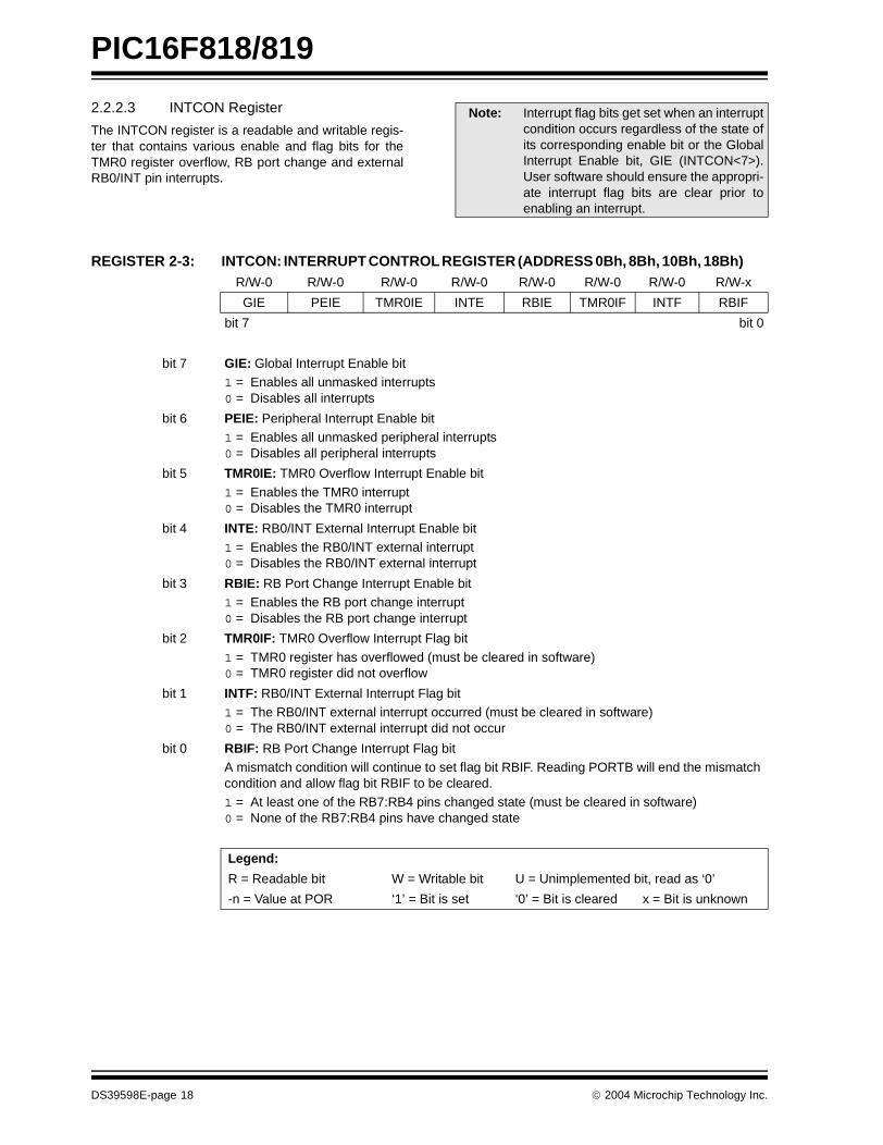
2.2.2.3 INTCON Register
The INTCON register is a readable and writable regis-ter that contains various enable and flag bits for theTMR0 register overflow, RB port change and externalRB0/INT pin interrupts.
REGISTER 2-3: INTCON: INTERRUPT CONTROL REGISTER (ADDRESS 0Bh, 8Bh, 10Bh, 18Bh)
Note: Interrupt flag bits get set when an interruptcondition occurs regardless of the state ofits corresponding enable bit or the GlobalInterrupt Enable bit, GIE (INTCON<7>).User software should ensure the appropri-ate interrupt flag bits are clear prior toenabling an interrupt.
R/W-0 R/W-0 R/W-0 R/W-0 R/W-0 R/W-0 R/W-0 R/W-x
GIE PEIE TMR0IE INTE RBIE TMR0IF INTF RBIF
bit 7 bit 0
bit 7 GIE: Global Interrupt Enable bit 1 = Enables all unmasked interrupts0 = Disables all interrupts
bit 6 PEIE: Peripheral Interrupt Enable bit1 = Enables all unmasked peripheral interrupts0 = Disables all peripheral interrupts
bit 5 TMR0IE: TMR0 Overflow Interrupt Enable bit
1 = Enables the TMR0 interrupt0 = Disables the TMR0 interrupt
bit 4 INTE: RB0/INT External Interrupt Enable bit1 = Enables the RB0/INT external interrupt0 = Disables the RB0/INT external interrupt
bit 3 RBIE: RB Port Change Interrupt Enable bit1 = Enables the RB port change interrupt0 = Disables the RB port change interrupt
bit 2 TMR0IF: TMR0 Overflow Interrupt Flag bit
1 = TMR0 register has overflowed (must be cleared in software)0 = TMR0 register did not overflow
bit 1 INTF: RB0/INT External Interrupt Flag bit1 = The RB0/INT external interrupt occurred (must be cleared in software)0 = The RB0/INT external interrupt did not occur
bit 0 RBIF: RB Port Change Interrupt Flag bitA mismatch condition will continue to set flag bit RBIF. Reading PORTB will end the mismatch condition and allow flag bit RBIF to be cleared.1 = At least one of the RB7:RB4 pins changed state (must be cleared in software)0 = None of the RB7:RB4 pins have changed state
Legend:
R = Readable bit W = Writable bit U = Unimplemented bit, read as ‘0’
-n = Value at POR ‘1’ = Bit is set ‘0’ = Bit is cleared x = Bit is unknown
DS39598E-page 18 2004 Microchip Technology Inc.

PIC16F818/819
2.2.2.4 PIE1 Register
This register contains the individual enable bits for theperipheral interrupts.
REGISTER 2-4: PIE1: PERIPHERAL INTERRUPT ENABLE REGISTER 1 (ADDRESS 8Ch)
Note: Bit PEIE (INTCON<6>) must be set toenable any peripheral interrupt.
U-0 R/W-0 U-0 U-0 R/W-0 R/W-0 R/W-0 R/W-0
— ADIE — — SSPIE CCP1IE TMR2IE TMR1IE
bit 7 bit 0
bit 7 Unimplemented: Read as ‘0’
bit 6 ADIE: A/D Converter Interrupt Enable bit
1 = Enables the A/D converter interrupt0 = Disables the A/D converter interrupt
bit 5-4 Unimplemented: Read as ‘0’
bit 3 SSPIE: Synchronous Serial Port Interrupt Enable bit1 = Enables the SSP interrupt0 = Disables the SSP interrupt
bit 2 CCP1IE: CCP1 Interrupt Enable bit
1 = Enables the CCP1 interrupt0 = Disables the CCP1 interrupt
bit 1 TMR2IE: TMR2 to PR2 Match Interrupt Enable bit1 = Enables the TMR2 to PR2 match interrupt0 = Disables the TMR2 to PR2 match interrupt
bit 0 TMR1IE: TMR1 Overflow Interrupt Enable bit1 = Enables the TMR1 overflow interrupt0 = Disables the TMR1 overflow interrupt
Legend:
R = Readable bit W = Writable bit U = Unimplemented bit, read as ‘0’
-n = Value at POR ‘1’ = Bit is set ‘0’ = Bit is cleared x = Bit is unknown
2004 Microchip Technology Inc. DS39598E-page 19

PIC16F818/819
2.2.2.5 PIR1 Register
This register contains the individual flag bits for theperipheral interrupts.
REGISTER 2-5: PIR1: PERIPHERAL INTERRUPT REQUEST (FLAG) REGISTER 1 (ADDRESS 0Ch)
Note: Interrupt flag bits are set when an interruptcondition occurs regardless of the state ofits corresponding enable bit or the GlobalInterrupt Enable bit, GIE (INTCON<7>).User software should ensure the appropri-ate interrupt flag bits are clear prior toenabling an interrupt.
U-0 R/W-0 U-0 U-0 R/W-0 R/W-0 R/W-0 R/W-0
— ADIF — — SSPIF CCP1IF TMR2IF TMR1IF
bit 7 bit 0
bit 7 Unimplemented: Read as ‘0’
bit 6 ADIF: A/D Converter Interrupt Flag bit1 = An A/D conversion completed0 = The A/D conversion is not complete
bit 5-4 Unimplemented: Read as ‘0’
bit 3 SSPIF: Synchronous Serial Port (SSP) Interrupt Flag bit1 = The SSP interrupt condition has occurred and must be cleared in software before returning
from the Interrupt Service Routine. The conditions that will set this bit are a transmission/reception has taken place.
0 = No SSP interrupt condition has occurred
bit 2 CCP1IF: CCP1 Interrupt Flag bitCapture mode:1 = A TMR1 register capture occurred (must be cleared in software)0 = No TMR1 register capture occurredCompare mode:1 = A TMR1 register compare match occurred (must be cleared in software)0 = No TMR1 register compare match occurred
PWM mode:Unused in this mode.
bit 1 TMR2IF: TMR2 to PR2 Match Interrupt Flag bit1 = TMR2 to PR2 match occurred (must be cleared in software)0 = No TMR2 to PR2 match occurred
bit 0 TMR1IF: TMR1 Overflow Interrupt Flag bit1 = TMR1 register overflowed (must be cleared in software)0 = TMR1 register did not overflow
Legend:
R = Readable bit W = Writable bit U = Unimplemented bit, read as ‘0’
-n = Value at POR ‘1’ = Bit is set ‘0’ = Bit is cleared x = Bit is unknown
DS39598E-page 20 2004 Microchip Technology Inc.
PIC16F818/819
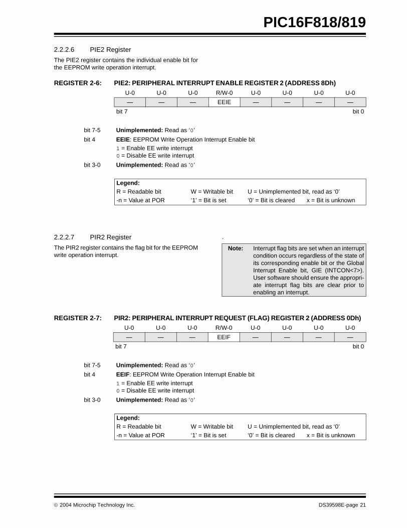
2.2.2.6 PIE2 Register
The PIE2 register contains the individual enable bit forthe EEPROM write operation interrupt.
REGISTER 2-6: PIE2: PERIPHERAL INTERRUPT ENABLE REGISTER 2 (ADDRESS 8Dh)
2.2.2.7 PIR2 Register
The PIR2 register contains the flag bit for the EEPROMwrite operation interrupt.
.
REGISTER 2-7: PIR2: PERIPHERAL INTERRUPT REQUEST (FLAG) REGISTER 2 (ADDRESS 0Dh)
U-0 U-0 U-0 R/W-0 U-0 U-0 U-0 U-0
— — — EEIE — — — —
bit 7 bit 0
bit 7-5 Unimplemented: Read as ‘0’
bit 4 EEIE: EEPROM Write Operation Interrupt Enable bit1 = Enable EE write interrupt0 = Disable EE write interrupt
bit 3-0 Unimplemented: Read as ‘0’
Legend:R = Readable bit W = Writable bit U = Unimplemented bit, read as ‘0’-n = Value at POR ‘1’ = Bit is set ‘0’ = Bit is cleared x = Bit is unknown
Note: Interrupt flag bits are set when an interruptcondition occurs regardless of the state ofits corresponding enable bit or the GlobalInterrupt Enable bit, GIE (INTCON<7>).User software should ensure the appropri-ate interrupt flag bits are clear prior toenabling an interrupt.
U-0 U-0 U-0 R/W-0 U-0 U-0 U-0 U-0
— — — EEIF — — — —
bit 7 bit 0
bit 7-5 Unimplemented: Read as ‘0’
bit 4 EEIF: EEPROM Write Operation Interrupt Enable bit
1 = Enable EE write interrupt0 = Disable EE write interrupt
bit 3-0 Unimplemented: Read as ‘0’
Legend:R = Readable bit W = Writable bit U = Unimplemented bit, read as ‘0’
-n = Value at POR ‘1’ = Bit is set ‘0’ = Bit is cleared x = Bit is unknown
2004 Microchip Technology Inc. DS39598E-page 21

PIC16F818/819
2.2.2.8 PCON Register
The Power Control (PCON) register contains a flag bitto allow differentiation between a Power-on Reset(POR), a Brown-out Reset, an external MCLR Resetand WDT Reset.
REGISTER 2-8: PCON: POWER CONTROL REGISTER (ADDRESS 8Eh)
Note: Interrupt flag bits get set when an interruptcondition occurs regardless of the state ofits corresponding enable bit or the GlobalInterrupt Enable bit, GIE (INTCON<7>).User software should ensure the appropri-ate interrupt flag bits are clear prior toenabling an interrupt.
Note: BOR is unknown on Power-on Reset. Itmust then be set by the user and checkedon subsequent Resets to see if BOR isclear, indicating a brown-out has occurred.The BOR status bit is a ‘don’t care’ and isnot necessarily predictable if the brown-out circuit is disabled (by clearing theBOREN bit in the Configuration word).
U-0 U-0 U-0 U-0 U-0 U-0 R/W-0 R/W-x
— — — — — — POR BOR
bit 7 bit 0
bit 7-2 Unimplemented: Read as ‘0’
bit 1 POR: Power-on Reset Status bit
1 = No Power-on Reset occurred0 = A Power-on Reset occurred (must be set in software after a Power-on Reset occurs)
bit 0 BOR: Brown-out Reset Status bit1 = No Brown-out Reset occurred0 = A Brown-out Reset occurred (must be set in software after a Brown-out Reset occurs)
Legend:
R = Readable bit W = Writable bit U = Unimplemented bit, read as ‘0’
-n = Value at POR ‘1’ = Bit is set ‘0’ = Bit is cleared x = Bit is unknown
DS39598E-page 22 2004 Microchip Technology Inc.
PIC16F818/819
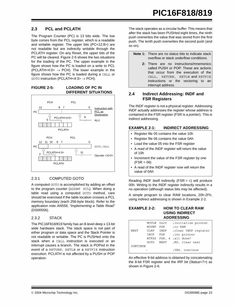
2.3 PCL and PCLATH
The Program Counter (PC) is 13 bits wide. The lowbyte comes from the PCL register, which is a readableand writable register. The upper bits (PC<12:8>) arenot readable but are indirectly writable through thePCLATH register. On any Reset, the upper bits of thePC will be cleared. Figure 2-5 shows the two situationsfor the loading of the PC. The upper example in thefigure shows how the PC is loaded on a write to PCL(PCLATH<4:0> → PCH). The lower example in thefigure shows how the PC is loaded during a CALL orGOTO instruction (PCLATH<4:3> → PCH).
FIGURE 2-5: LOADING OF PC IN DIFFERENT SITUATIONS
2.3.1 COMPUTED GOTO
A computed GOTO is accomplished by adding an offsetto the program counter (ADDWF PCL). When doing atable read using a computed GOTO method, careshould be exercised if the table location crosses a PCLmemory boundary (each 256-byte block). Refer to theapplication note AN556, “Implementing a Table Read”(DS00556).
2.3.2 STACK
The PIC16F818/819 family has an 8-level deep x 13-bitwide hardware stack. The stack space is not part ofeither program or data space and the Stack Pointer isnot readable or writable. The PC is PUSHed onto thestack when a CALL instruction is executed or aninterrupt causes a branch. The stack is POPed in theevent of a RETURN, RETLW or a RETFIE instructionexecution. PCLATH is not affected by a PUSH or POPoperation.
The stack operates as a circular buffer. This means thatafter the stack has been PUSHed eight times, the ninthpush overwrites the value that was stored from the firstpush. The tenth push overwrites the second push (andso on).
2.4 Indirect Addressing: INDF and FSR Registers
The INDF register is not a physical register. AddressingINDF actually addresses the register whose address iscontained in the FSR register (FSR is a pointer). This isindirect addressing.
EXAMPLE 2-1: INDIRECT ADDRESSING
Reading INDF itself indirectly (FSR = 0) will produce00h. Writing to the INDF register indirectly results in ano operation (although status bits may be affected).
A simple program to clear RAM locations, 20h-2Fh,using indirect addressing is shown in Example 2-2.
EXAMPLE 2-2: HOW TO CLEAR RAM USING INDIRECT ADDRESSING
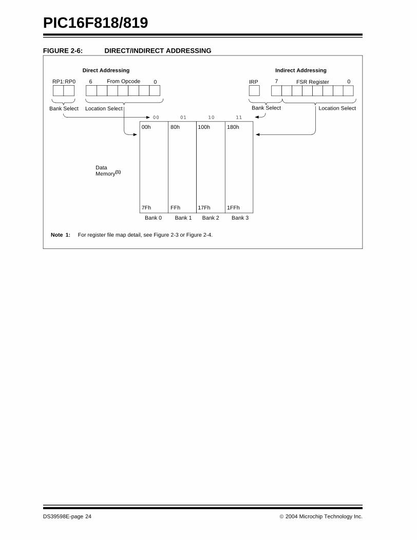
An effective 9-bit address is obtained by concatenatingthe 8-bit FSR register and the IRP bit (Status<7>) asshown in Figure 2-6.
PC
12 8 7 0
5PCLATH<4:0>
PCLATH
Instruction with
ALU
GOTO,CALL
Opcode <10:0>
8
PC
12 11 10 0
11PCLATH<4:3>
PCH PCL
8 7
2
PCLATH
PCH PCL
PCL asDestination
Note 1: There are no status bits to indicate stackoverflow or stack underflow conditions.
2: There are no instructions/mnemonicscalled PUSH or POP. These are actionsthat occur from the execution of theCALL, RETURN, RETLW and RETFIEinstructions or the vectoring to aninterrupt address.
• Register file 05 contains the value 10h• Register file 06 contains the value 0Ah• Load the value 05 into the FSR register
• A read of the INDF register will return the value of 10h
• Increment the value of the FSR register by one (FSR = 06)
• A read of the INDF register now will return the value of 0Ah
MOVLW 0x20 ;initialize pointerMOVWF FSR ;to RAM
NEXT CLRF INDF ;clear INDF registerINCF FSR ;inc pointerBTFSS FSR, 4 ;all done?GOTO NEXT ;NO, clear next
CONTINUE : ;YES, continue
2004 Microchip Technology Inc. DS39598E-page 23
PIC16F818/819
FIGURE 2-6: DIRECT/INDIRECT ADDRESSING
Note 1: For register file map detail, see Figure 2-3 or Figure 2-4.
DataMemory(1)
Indirect AddressingDirect Addressing
Bank Select Location Select
RP1:RP0 6 0From Opcode IRP FSR Register7 0
Bank Select Location Select
00 01 10 11
Bank 0 Bank 1 Bank 2 Bank 3
FFh
80h
7Fh
00h
17Fh
100h
1FFh
180h
DS39598E-page 24 2004 Microchip Technology Inc.

PIC16F818/819
3.0 DATA EEPROM AND FLASH PROGRAM MEMORY
The data EEPROM and Flash program memory arereadable and writable during normal operation (overthe full VDD range). This memory is not directly mappedin the register file space. Instead, it is indirectlyaddressed through the Special Function Registers.There are six SFRs used to read and write thismemory:
• EECON1
• EECON2• EEDATA• EEDATH
• EEADR• EEADRH
This section focuses on reading and writing dataEEPROM and Flash program memory during normaloperation. Refer to the appropriate device program-ming specification document for serial programminginformation.
When interfacing the data memory block, EEDATAholds the 8-bit data for read/write and EEADR holds theaddress of the EEPROM location being accessed.These devices have 128 or 256 bytes of dataEEPROM, with an address range from 00h to 0FFh.Addresses from 80h to FFh are unimplemented on thePIC16F818 device and will read 00h. When writing tounimplemented locations, the charge pump will beturned off.
When interfacing the program memory block, theEEDATA and EEDATH registers form a two-byte wordthat holds the 14-bit data for read/write and the EEADRand EEADRH registers form a two-byte word that holdsthe 13-bit address of the EEPROM location beingaccessed. These devices have 1K or 2K words ofprogram Flash, with an address range from 0000h to03FFh for the PIC16F818 and 0000h to 07FFh for thePIC16F819. Addresses above the range of the respec-tive device will wraparound to the beginning of programmemory.
The EEPROM data memory allows single byte readand write. The Flash program memory allows single-word reads and four-word block writes. Programmemory writes must first start with a 32-word blockerase, then write in 4-word blocks. A byte write in dataEEPROM memory automatically erases the locationand writes the new data (erase before write).
The write time is controlled by an on-chip timer. Thewrite/erase voltages are generated by an on-chipcharge pump, rated to operate over the voltage rangeof the device for byte or word operations.
When the device is code-protected, the CPU maycontinue to read and write the data EEPROM memory.Depending on the settings of the write-protect bits, thedevice may or may not be able to write certain blocksof the program memory; however, reads of the programmemory are allowed. When code-protected, the deviceprogrammer can no longer access data or programmemory; this does NOT inhibit internal reads or writes.
3.1 EEADR and EEADRH
The EEADRH:EEADR register pair can address up toa maximum of 256 bytes of data EEPROM or up to amaximum of 8K words of program EEPROM. Whenselecting a data address value, only the LSB of theaddress is written to the EEADR register. When select-ing a program address value, the MSB of the addressis written to the EEADRH register and the LSB iswritten to the EEADR register.
If the device contains less memory than the full addressreach of the address register pair, the Most Significantbits of the registers are not implemented. For example,if the device has 128 bytes of data EEPROM, the MostSignificant bit of EEADR is not implemented on accessto data EEPROM.
3.2 EECON1 and EECON2 Registers
EECON1 is the control register for memory accesses.
Control bit, EEPGD, determines if the access will be aprogram or data memory access. When clear, as it iswhen Reset, any subsequent operations will operateon the data memory. When set, any subsequentoperations will operate on the program memory.
Control bits, RD and WR, initiate read and write,respectively. These bits cannot be cleared, only set insoftware. They are cleared in hardware at completionof the read or write operation. The inability to clear theWR bit in software prevents the accidental, prematuretermination of a write operation.
The WREN bit, when set, will allow a write or eraseoperation. On power-up, the WREN bit is clear. TheWRERR bit is set when a write (or erase) operation isinterrupted by a MCLR or a WDT Time-out Resetduring normal operation. In these situations, followingReset, the user can check the WRERR bit and rewritethe location. The data and address will be unchangedin the EEDATA and EEADR registers.
Interrupt flag bit, EEIF in the PIR2 register, is set whenthe write is complete. It must be cleared in software.
EECON2 is not a physical register. Reading EECON2will read all ‘0’s. The EECON2 register is usedexclusively in the EEPROM write sequence.
2004 Microchip Technology Inc. DS39598E-page 25

PIC16F818/819
REGISTER 3-1: EECON1: EEPROM ACCESS CONTROL REGISTER 1 (ADDRESS 18Ch) R/W-x U-0 U-0 R/W-x R/W-x R/W-0 R/S-0 R/S-0
EEPGD — — FREE WRERR WREN WR RD
bit 7 bit 0
bit 7 EEPGD: Program/Data EEPROM Select bit1 = Accesses program memory0 = Accesses data memoryReads ‘0’ after a POR; this bit cannot be changed while a write operation is in progress.
bit 6-5 Unimplemented: Read as ‘0’
bit 4 FREE: EEPROM Forced Row Erase bit1 = Erase the program memory row addressed by EEADRH:EEADR on the next WR command0 = Perform write-only
bit 3 WRERR: EEPROM Error Flag bit
1 = A write operation is prematurely terminated (any MCLR or any WDT Reset during normaloperation)
0 = The write operation completed
bit 2 WREN: EEPROM Write Enable bit1 = Allows write cycles0 = Inhibits write to the EEPROM
bit 1 WR: Write Control bit
1 = Initiates a write cycle. The bit is cleared by hardware once write is complete. The WR bitcan only be set (not cleared) in software.
0 = Write cycle to the EEPROM is complete
bit 0 RD: Read Control bit1 = Initiates an EEPROM read, RD is cleared in hardware. The RD bit can only be set (not
cleared) in software.0 = Does not initiate an EEPROM read
Legend:
R = Readable bit W = Writable bit S = Set only U = Unimplemented bit, read as ‘0’
-n = Value at POR ‘1’ = Bit is set ‘0’ = Bit is cleared x = Bit is unknown
DS39598E-page 26 2004 Microchip Technology Inc.

PIC16F818/819
3.3 Reading Data EEPROM Memory
To read a data memory location, the user must write theaddress to the EEADR register, clear the EEPGDcontrol bit (EECON1<7>) and then set control bit, RD(EECON1<0>). The data is available in the very nextcycle in the EEDATA register; therefore, it can be readin the next instruction (see Example 3-1). EEDATA willhold this value until another read or until it is written toby the user (during a write operation).
The steps to reading the EEPROM data memory are:
1. Write the address to EEADR. Make sure that theaddress is not larger than the memory size ofthe device.
2. Clear the EEPGD bit to point to EEPROM datamemory.
3. Set the RD bit to start the read operation.4. Read the data from the EEDATA register.
EXAMPLE 3-1: DATA EEPROM READ
3.4 Writing to Data EEPROM Memory
To write an EEPROM data location, the user must firstwrite the address to the EEADR register and the datato the EEDATA register. Then, the user must follow aspecific write sequence to initiate the write for eachbyte.
The write will not initiate if the write sequence is notexactly followed (write 55h to EECON2, write AAh toEECON2, then set WR bit) for each byte. We stronglyrecommend that interrupts be disabled during thiscode segment (see Example 3-2).
Additionally, the WREN bit in EECON1 must be set toenable write. This mechanism prevents accidentalwrites to data EEPROM due to errant (unexpected)code execution (i.e., lost programs). The user shouldkeep the WREN bit clear at all times except whenupdating EEPROM. The WREN bit is not clearedby hardware
After a write sequence has been initiated, clearing theWREN bit will not affect this write cycle. The WR bit willbe inhibited from being set unless the WREN bit is set.At the completion of the write cycle, the WR bit iscleared in hardware and the EE Write CompleteInterrupt Flag bit (EEIF) is set. The user can eitherenable this interrupt or poll this bit. EEIF must becleared by software.
The steps to write to EEPROM data memory are:
1. If step 10 is not implemented, check the WR bitto see if a write is in progress.
2. Write the address to EEADR. Make sure that theaddress is not larger than the memory size ofthe device.
3. Write the 8-bit data value to be programmed inthe EEDATA register.
4. Clear the EEPGD bit to point to EEPROM datamemory.
5. Set the WREN bit to enable program operations.6. Disable interrupts (if enabled).7. Execute the special five instruction sequence:
• Write 55h to EECON2 in two steps (first to W, then to EECON2)
• Write AAh to EECON2 in two steps (first to W, then to EECON2)
• Set the WR bit8. Enable interrupts (if using interrupts).9. Clear the WREN bit to disable program
operations.10. At the completion of the write cycle, the WR bit
is cleared and the EEIF interrupt flag bit is set(EEIF must be cleared by firmware). If step 1 isnot implemented, then firmware should checkfor EEIF to be set, or WR to be clear, to indicatethe end of the program cycle.
EXAMPLE 3-2: DATA EEPROM WRITE
BANKSEL EEADR ; Select Bank of EEADRMOVF ADDR, W ; MOVWF EEADR ; Data Memory Address
; to readBANKSEL EECON1 ; Select Bank of EECON1BCF EECON1, EEPGD ; Point to Data memoryBSF EECON1, RD ; EE ReadBANKSEL EEDATA ; Select Bank of EEDATAMOVF EEDATA, W ; W = EEDATA
BANKSEL EECON1 ; Select Bank of; EECON1
BTFSC EECON1, WR ; Wait for writeGOTO $-1 ; to completeBANKSEL EEADR ; Select Bank of
; EEADRMOVF ADDR, W ; MOVWF EEADR ; Data Memory
; Address to writeMOVF VALUE, W ; MOVWF EEDATA ; Data Memory Value
; to writeBANKSEL EECON1 ; Select Bank of
; EECON1BCF EECON1, EEPGD ; Point to DATA
; memoryBSF EECON1, WREN ; Enable writes
BCF INTCON, GIE ; Disable INTs.MOVLW 55h ; MOVWF EECON2 ; Write 55hMOVLW AAh ; MOVWF EECON2 ; Write AAhBSF EECON1, WR ; Set WR bit to
; begin writeBSF INTCON, GIE ; Enable INTs.BCF EECON1, WREN ; Disable writes
Req
uire
dS
eque
nce
2004 Microchip Technology Inc. DS39598E-page 27

PIC16F818/819
3.5 Reading Flash Program Memory
To read a program memory location, the user mustwrite two bytes of the address to the EEADR andEEADRH registers, set the EEPGD control bit(EECON1<7>) and then set control bit, RD(EECON1<0>). Once the read control bit is set, theprogram memory Flash controller will use the secondinstruction cycle to read the data. This causes thesecond instruction immediately following the“BSF EECON1, RD” instruction to be ignored. The datais available in the very next cycle in the EEDATA andEEDATH registers; therefore, it can be read as twobytes in the following instructions. EEDATA andEEDATH registers will hold this value until another reador until it is written to by the user (during a writeoperation).
EXAMPLE 3-3: FLASH PROGRAM READ
3.6 Erasing Flash Program Memory
The minimum erase block is 32 words. Only throughthe use of an external programmer, or through ICSPcontrol, can larger blocks of program memory be bulkerased. Word erase in the Flash array is not supported.
When initiating an erase sequence from the micro-controller itself, a block of 32 words of program memoryis erased. The Most Significant 11 bits of theEEADRH:EEADR point to the block being erased.EEADR< 4:0> are ignored.
The EECON1 register commands the erase operation.The EEPGD bit must be set to point to the Flashprogram memory. The WREN bit must be set to enablewrite operations. The FREE bit is set to select an eraseoperation.
For protection, the write initiate sequence for EECON2must be used.
After the “BSF EECON1, WR” instruction, the processorrequires two cycles to set up the erase operation. Theuser must place two NOP instructions after the WR bit isset. The processor will halt internal operations for thetypical 2 ms, only during the cycle in which the erasetakes place. This is not Sleep mode, as the clocks andperipherals will continue to run. After the erase cycle,the processor will resume operation with the thirdinstruction after the EECON1 write instruction.
3.6.1 FLASH PROGRAM MEMORY ERASE SEQUENCE
The sequence of events for erasing a block of internalprogram memory location is:
1. Load EEADRH:EEADR with address of rowbeing erased.
2. Set EEPGD bit to point to program memory; setWREN bit to enable writes and set FREE bit toenable the erase.
3. Disable interrupts.4. Write 55h to EECON2.
5. Write AAh to EECON2.6. Set the WR bit. This will begin the row erase
cycle.7. The CPU will stall for duration of the erase.
BANKSEL EEADRH ; Select Bank of EEADRHMOVF ADDRH, W ; MOVWF EEADRH ; MS Byte of Program
; Address to readMOVF ADDRL, W ; MOVWF EEADR ; LS Byte of Program
; Address to readBANKSEL EECON1 ; Select Bank of EECON1BSF EECON1, EEPGD; Point to PROGRAM
; memoryBSF EECON1, RD ; EE Read
; NOP ; Any instructions
; here are ignored as NOP ; program memory is
; read in second cycle; after BSF EECON1,RD
BANKSEL EEDATA ; Select Bank of EEDATAMOVF EEDATA, W ; DATAL = EEDATAMOVWF DATAL ; MOVF EEDATH, W ; DATAH = EEDATHMOVWF DATAH ;
DS39598E-page 28 2004 Microchip Technology Inc.

PIC16F818/819
EXAMPLE 3-4: ERASING A FLASH PROGRAM MEMORY ROW BANKSEL EEADRH ; Select Bank of EEADRHMOVF ADDRH, W ; MOVWF EEADRH ; MS Byte of Program Address to EraseMOVF ADDRL, W ; MOVWF EEADR ; LS Byte of Program Address to Erase
ERASE_ROWBANKSEL EECON1 ; Select Bank of EECON1BSF EECON1, EEPGD ; Point to PROGRAM memoryBSF EECON1, WREN ; Enable Write to memoryBSF EECON1, FREE ; Enable Row Erase operation
;BCF INTCON, GIE ; Disable interrupts (if using)MOVLW 55h ; MOVWF EECON2 ; Write 55hMOVLW AAh ; MOVWF EECON2 ; Write AAhBSF EECON1, WR ; Start Erase (CPU stall)NOP ; Any instructions here are ignored as processor
; halts to begin Erase sequenceNOP ; processor will stop here and wait for Erase complete
; after Erase processor continues with 3rd instructionBCF EECON1, FREE ; Disable Row Erase operationBCF EECON1, WREN ; Disable writesBSF INTCON, GIE ; Enable interrupts (if using)
2004 Microchip Technology Inc. DS39598E-page 29

PIC16F818/819
3.7 Writing to Flash Program MemoryFlash program memory may only be written to if thedestination address is in a segment of memory that isnot write-protected, as defined in bits WRT1:WRT0 ofthe device Configuration Word (Register 12-1). Flashprogram memory must be written in four-word blocks.A block consists of four words with sequentialaddresses, with a lower boundary defined by anaddress, where EEADR<1:0> = 00. At the same time,all block writes to program memory are done as write-only operations. The program memory must first beerased. The write operation is edge-aligned and cannotoccur across boundaries.
To write to the program memory, the data must first beloaded into the buffer registers. There are four 14-bitbuffer registers and they are addressed by the low2 bits of EEADR.
The following sequence of events illustrate how toperform a write to program memory:
• Set the EEPGD and WREN bits in the EECON1 register
• Clear the FREE bit in EECON1• Write address to EEADRH:EEADR• Write data to EEDATH:EEDATA
• Write 55 to EECON2• Write AA to EECON2• Set WR bit in EECON 1
The user must follow the same specific sequence toinitiate the write for each word in the program block bywriting each program word in sequence (00, 01, 10,11).
There are 4 buffer register words and all four locationsMUST be written to with correct data.
After the “BSF EECON1, WR” instruction, ifEEADR ≠ xxxxxx11, then a short write will occur.This short write-only transfers the data to the bufferregister. The WR bit will be cleared in hardware afterone cycle.
After the “BSF EECON1, WR” instruction, ifEEADR = xxxxxx11, then a long write will occur. Thiswill simultaneously transfer the data fromEEDATH:EEDATA to the buffer registers and begin thewrite of all four words. The processor will execute thenext instruction and then ignore the subsequentinstruction. The user should place NOP instructions intothe second words. The processor will then halt internaloperations for typically 2 msec in which the write takesplace. This is not a Sleep mode, as the clocks andperipherals will continue to run. After the write cycle,the processor will resume operation with the 3rdinstruction after the EECON1 write instruction.
After each long write, the 4 buffer registers will be resetto 3FFF.
FIGURE 3-1: BLOCK WRITES TO FLASH PROGRAM MEMORY
14 14 14 14
Program Memory
Buffer Register
EEADR<1:0> = 00
Buffer Register
EEADR<1:0> = 01
Buffer Register
EEADR<1:0> = 10
Buffer Register
EEADR<1:0> = 11
EEDATAEEDATH
7 5 0 7 0
6 8
First word of blockto be written
to Flash automaticallyafter this wordis written
transferred
All buffers are
DS39598E-page 30 2004 Microchip Technology Inc.

PIC16F818/819
An example of the complete four-word write sequenceis shown in Example 3-5. The initial address is loadedinto the EEADRH:EEADR register pair; the four wordsof data are loaded using indirect addressing, assumingthat a row erase sequence has already beenperformed.
EXAMPLE 3-5: WRITING TO FLASH PROGRAM MEMORY ; This write routine assumes the following:
; 1. The 32 words in the erase block have already been erased.; 2. A valid starting address (the least significant bits = '00') is loaded into EEADRH:EEADR; 3. This example is starting at 0x100, this is an application dependent setting.; 4. The 8 bytes (4 words) of data are loaded, starting at an address in RAM called ARRAY.; 5. This is an example only, location of data to program is application dependent.; 6. word_block is located in data memory.
BANKSEL EECON1 ;prepare for WRITE procedureBSF EECON1, EEPGD ;point to program memoryBSF EECON1, WREN ;allow write cyclesBCF EECON1, FREE ;perform write only
BANKSEL word_blockMOVLW .4MOVWF word_block ;prepare for 4 words to be written
BANKSEL EEADRH ;Start writing at 0x100MOVLW 0x01MOVWF EEADRH ;load HIGH addressMOVLW 0x00MOVWF EEADR ;load LOW addressBANKSEL ARRAYMOVLW ARRAY ;initialize FSR to start of dataMOVWF FSR
LOOPBANKSEL EEDATAMOVF INDF, W ;indirectly load EEDATAMOVWF EEDATAINCF FSR, F ;increment data pointerMOVF INDF, W ;indirectly load EEDATHMOVWF EEDATHINCF FSR, F ;increment data pointer
BANKSEL EECON1MOVLW 0x55 ;required sequenceMOVWF EECON2MOVLW 0xAAMOVWF EECON2BSF EECON1, WR ;set WR bit to begin writeNOP ;instructions here are ignored as processor NOP
BANKSEL EEADRINCF EEADR, f ;load next word addressBANKSEL word_blockDECFSZ word_block, f ;have 4 words been written?GOTO loop ;NO, continue with writing
BANKSEL EECON1BCF EECON1, WREN ;YES, 4 words complete, disable writesBSF INTCON, GIE ;enable interrupts
Req
uire
dS
eque
nce
2004 Microchip Technology Inc. DS39598E-page 31

PIC16F818/819
3.8 Protection Against Spurious Write
There are conditions when the device should not writeto the data EEPROM memory. To protect againstspurious EEPROM writes, various mechanisms havebeen built-in. On power-up, WREN is cleared. Also, thePower-up Timer (72 ms duration) prevents anEEPROM write.
The write initiate sequence and the WREN bit togetherhelp prevent an accidental write during brown-out,power glitch or software malfunction.
3.9 Operation During Code-Protect
When the data EEPROM is code-protected, the micro-controller can read and write to the EEPROM normally.However, all external access to the EEPROM isdisabled. External write access to the program memoryis also disabled.
When program memory is code-protected, the micro-controller can read and write to program memorynormally as well as execute instructions. Writes by thedevice may be selectively inhibited to regions ofthe memory depending on the setting of bits,WRT1:WRT0, of the Configuration Word (seeSection 12.1 “Configuration Bits” for additionalinformation). External access to the memory is alsodisabled.
TABLE 3-1: REGISTERS/BITS ASSOCIATED WITH DATA EEPROM AND FLASH PROGRAM MEMORIES
Address Name Bit 7 Bit 6 Bit 5 Bit 4 Bit 3 Bit 2 Bit 1 Bit 0Value on Power-on
Reset
Value on all other Resets
10Ch EEDATA EEPROM/Flash Data Register Low Byte xxxx xxxx uuuu uuuu
10Dh EEADR EEPROM/Flash Address Register Low Byte xxxx xxxx uuuu uuuu
10Eh EEDATH — — EEPROM/Flash Data Register High Byte --xx xxxx --uu uuuu
10Fh EEADRH — — — — — EEPROM/Flash Address Register High Byte
---- -xxx ---- -uuu
18Ch EECON1 EEPGD — — FREE WRERR WREN WR RD x--x x000 x--x q000
18Dh EECON2 EEPROM Control Register 2 (not a physical register) ---- ---- ---- ----
0Dh PIR2 — — — EEIF — — — — ---0 ---- ---0 ----
8Dh PIE2 — — — EEIE — — — — ---0 ---- ---0 ----
Legend: x = unknown, u = unchanged, - = unimplemented, read as ‘0’, q = value depends upon condition. Shaded cells are not used by data EEPROM or Flash program memory.
DS39598E-page 32 2004 Microchip Technology Inc.

PIC16F818/819
4.0 OSCILLATOR CONFIGURATIONS
4.1 Oscillator Types
The PIC16F818/819 can be operated in eight differentoscillator modes. The user can program three configu-ration bits (FOSC2:FOSC0) to select one of these eightmodes (modes 5-8 are new PIC16 oscillatorconfigurations):
1. LP Low-Power Crystal
2. XT Crystal/Resonator3. HS High-Speed Crystal/Resonator4. RC External Resistor/Capacitor with
FOSC/4 output on RA65. RCIO External Resistor/Capacitor with
I/O on RA66. INTIO1 Internal Oscillator with FOSC/4
output on RA6 and I/O on RA77. INTIO2 Internal Oscillator with I/O on RA6
and RA78. ECIO External Clock with I/O on RA6
4.2 Crystal Oscillator/Ceramic Resonators
In XT, LP or HS modes, a crystal or ceramic resonatoris connected to the OSC1/CLKI and OSC2/CLKO pinsto establish oscillation (see Figure 4-1 and Figure 4-2).The PIC16F818/819 oscillator design requires the useof a parallel cut crystal. Use of a series cut crystal maygive a frequency out of the crystal manufacturer’sspecifications.
FIGURE 4-1: CRYSTAL OPERATION (HS, XT OR LP OSC CONFIGURATION)
TABLE 4-1: CAPACITOR SELECTION FOR CRYSTAL OSCILLATOR (FOR DESIGN GUIDANCE ONLY)
Note 1: See Table 4-1 for typical values of C1 and C2.
2: A series resistor (RS) may be required for ATstrip cut crystals.
3: RF varies with the crystal chosen (typicallybetween 2 MΩ to 10 MΩ).
C1(1)
C2(1)
XTAL
OSC2
RS(2)
OSC1
RF(3) Sleep
To Internal Logic
PIC16F818/819
Osc TypeCrystal
Freq
Typical Capacitor Values Tested:
C1 C2
LP 32 kHz 33 pF 33 pF
200 kHz 15 pF 15 pF
XT 200 kHz 56 pF 56 pF
1 MHz 15 pF 15 pF
4 MHz 15 pF 15 pF
HS 4 MHz 15 pF 15 pF
8 MHz 15 pF 15 pF
20 MHz 15 pF 15 pF
Capacitor values are for design guidance only.
These capacitors were tested with the crystals listedbelow for basic start-up and operation. These valueswere not optimized.
Different capacitor values may be required to produceacceptable oscillator operation. The user should testthe performance of the oscillator over the expectedVDD and temperature range for the application.
See the notes following this table for additionalinformation.
Note 1: Higher capacitance increases the stabilityof the oscillator but also increases thestart-up time.
2: Since each crystal has its own character-istics, the user should consult the crystalmanufacturer for appropriate values ofexternal components.
3: RS may be required in HS mode, as wellas XT mode, to avoid overdriving crystalswith low drive level specification.
4: Always verify oscillator performance overthe VDD and temperature range that isexpected for the application.
2004 Microchip Technology Inc. DS39598E-page 33

PIC16F818/819
FIGURE 4-2: CERAMIC RESONATOR OPERATION (HS OR XT OSC CONFIGURATION)
TABLE 4-2: CERAMIC RESONATORS (FOR DESIGN GUIDANCE ONLY)
4.3 External Clock Input
The ECIO Oscillator mode requires an external clocksource to be connected to the OSC1 pin. There is nooscillator start-up time required after a Power-on Resetor after an exit from Sleep mode.
In the ECIO Oscillator mode, the OSC2 pin becomesan additional general purpose I/O pin. The I/O pinbecomes bit 6 of PORTA (RA6). Figure 4-3 shows thepin connections for the ECIO Oscillator mode.
FIGURE 4-3: EXTERNAL CLOCK INPUT OPERATION (ECIO CONFIGURATION)
Typical Capacitor Values Used:
Mode Freq OSC1 OSC2
XT 455 kHz2.0 MHz4.0 MHz
56 pF47 pF33 pF
56 pF47 pF33 pF
HS 8.0 MHz16.0 MHz
27 pF22 pF
27 pF22 pF
Capacitor values are for design guidance only.
These capacitors were tested with the resonatorslisted below for basic start-up and operation. Thesevalues were not optimized.
Different capacitor values may be required to produceacceptable oscillator operation. The user should testthe performance of the oscillator over the expectedVDD and temperature range for the application.
See the notes following this table for additionalinformation.
Note: When using resonators with frequenciesabove 3.5 MHz, the use of HS mode ratherthan XT mode is recommended. HS modemay be used at any VDD for which thecontroller is rated. If HS is selected, it ispossible that the gain of the oscillator willoverdrive the resonator. Therefore, aseries resistor should be placed betweenthe OSC2 pin and the resonator. As agood starting point, the recommendedvalue of RS is 330Ω.
Note 1: See Table 4-2 for typical values of C1 and C2.
2: A series resistor (RS) may be required.
3: RF varies with the resonator chosen (typicallybetween 2 MΩ to 10 MΩ).
C1(1)
C2(1)
RES
OSC2
RS(2)
OSC1
RF(3) Sleep
To Internal Logic
PIC16F818/819
OSC1/CLKI
I/O (OSC2)RA6
Clock fromExt. System PIC16F818/819
DS39598E-page 34 2004 Microchip Technology Inc.

PIC16F818/819
4.4 RC Oscillator
For timing insensitive applications, the “RC” and“RCIO” device options offer additional cost savings.The RC oscillator frequency is a function of the supplyvoltage, the resistor (REXT) and capacitor (CEXT)values and the operating temperature. In addition tothis, the oscillator frequency will vary from unit to unitdue to normal manufacturing variation. Furthermore,the difference in lead frame capacitance between pack-age types will also affect the oscillation frequency,especially for low CEXT values. The user also needs totake into account variation due to tolerance of externalR and C components used. Figure 4-4 shows how theR/C combination is connected.
In the RC Oscillator mode, the oscillator frequencydivided by 4 is available on the OSC2 pin. This signal maybe used for test purposes or to synchronize other logic.
FIGURE 4-4: RC OSCILLATOR MODE
The RCIO Oscillator mode (Figure 4-5) functions likethe RC mode except that the OSC2 pin becomes anadditional general purpose I/O pin. The I/O pinbecomes bit 6 of PORTA (RA6).
FIGURE 4-5: RCIO OSCILLATOR MODE
4.5 Internal Oscillator Block
The PIC16F818/819 devices include an internaloscillator block which generates two different clocksignals; either can be used as the system’s clocksource. This can eliminate the need for externaloscillator circuits on the OSC1 and/or OSC2 pins.
The main output (INTOSC) is an 8 MHz clock sourcewhich can be used to directly drive the system clock. Italso drives the INTOSC postscaler which can provide arange of clock frequencies from 125 kHz to 4 MHz.
The other clock source is the internal RC oscillator(INTRC) which provides a 31.25 kHz (32 µs nominalperiod) output. The INTRC oscillator is enabled byselecting the INTRC as the system clock source orwhen any of the following are enabled:
• Power-up Timer • Watchdog Timer
These features are discussed in greater detail inSection 12.0 “Special Features of the CPU”.
The clock source frequency (INTOSC direct, INTRCdirect or INTOSC postscaler) is selected by configuringthe IRCF bits of the OSCCON register (Register 4-2).
4.5.1 INTRC MODES
Using the internal oscillator as the clock source caneliminate the need for up to two external oscillator pins,which can then be used for digital I/O. Two distinctconfigurations are available:
• In INTIO1 mode, the OSC2 pin outputs FOSC/4 while OSC1 functions as RA7 for digital input and output.
• In INTIO2 mode, OSC1 functions as RA7 and OSC2 functions as RA6, both for digital input and output.
OSC2/CLKO
CEXT
REXT
PIC16F818/819
OSC1
FOSC/4
InternalClock
VDD
VSS
Recommended values: 3 kΩ ≤ REXT ≤ 100 kΩCEXT > 20 pF
CEXT
REXT
PIC16F818/819
OSC1 InternalClock
VDD
VSS
Recommended values: 3 kΩ ≤ REXT ≤ 100 kΩCEXT > 20 pF
I/O (OSC2)RA6
Note: Throughout this data sheet, when referringspecifically to a generic clock source, theterm “INTRC” may also be used to refer tothe clock modes using the internaloscillator block. This is regardless ofwhether the actual frequency used isINTOSC (8 MHz), the INTOSC postscaleror INTRC (31.25 kHz).
2004 Microchip Technology Inc. DS39598E-page 35

PIC16F818/819
4.5.2 OSCTUNE REGISTER
The internal oscillator’s output has been calibrated at thefactory but can be adjusted in the application. This isdone by writing to the OSCTUNE register (Register 4-1).The tuning sensitivity is constant throughout the tuningrange. The OSCTUNE register has a tuning range of±12.5%.
When the OSCTUNE register is modified, the INTOSCand INTRC frequencies will begin shifting to the new fre-quency. The INTRC clock will reach the new frequencywithin 8 clock cycles (approximately 8 * 32 µs = 256 µs);the INTOSC clock will stabilize within 1 ms. Code execu-tion continues during this shift. There is no indication thatthe shift has occurred. Operation of features that dependon the 31.25 kHz INTRC clock source frequency, suchas the WDT, Fail-Safe Clock Monitor and peripherals,will also be affected by the change in frequency.
REGISTER 4-1: OSCTUNE: OSCILLATOR TUNING REGISTER (ADDRESS 90h) U-0 U-0 R/W-0 R/W-0 R/W-0 R/W-0 R/W-0 R/W-0
— — TUN5 TUN4 TUN3 TUN2 TUN1 TUN0
bit 7 bit 0
bit 7-6 Unimplemented: Read as ‘0’bit 5-0 TUN<5:0>: Frequency Tuning bits
011111 = Maximum frequency011110 = •••000001 = 000000 = Center frequency. Oscillator module is running at the calibrated frequency.111111 = •••100000 = Minimum frequency
Legend:R = Readable bit W = Writable bit U = Unimplemented bit, read as ‘0’-n = Value at POR ‘1’ = Bit is set ‘0’ = Bit is cleared x = Bit is unknown
DS39598E-page 36 2004 Microchip Technology Inc.

PIC16F818/819
4.5.3 OSCILLATOR CONTROL REGISTER
The OSCCON register (Register 4-2) controls severalaspects of the system clock’s operation.
The Internal Oscillator Select bits, IRCF2:IRCF0, selectthe frequency output of the internal oscillator block thatis used to drive the system clock. The choices are theINTRC source (31.25 kHz), the INTOSC source(8 MHz) or one of the six frequencies derived from theINTOSC postscaler (125 kHz to 4 MHz). Changing theconfiguration of these bits has an immediate change onthe multiplexor’s frequency output.
4.5.4 MODIFYING THE IRCF BITS
The IRCF bits can be modified at any time regardless ofwhich clock source is currently being used as thesystem clock. The internal oscillator allows users tochange the frequency during run time. This is achievedby modifying the IRCF bits in the OSCCON register.The sequence of events that occur after the IRCF bitsare modified is dependent upon the initial value of theIRCF bits before they are modified. If the INTRC(31.25 kHz, IRCF<2:0> = 000) is running and the IRCFbits are modified to any other value than ‘000’, a 4 ms(approx.) clock switch delay is turned on. Code execu-tion continues at a higher than expected frequencywhile the new frequency stabilizes. Time sensitive codeshould wait for the IOFS bit in the OSCCON register tobecome set before continuing. This bit can bemonitored to ensure that the frequency is stable beforeusing the system clock in time critical applications.
If the IRCF bits are modified while the internal oscillatoris running at any other frequency than INTRC(31.25 kHz, IRCF<2:0> ≠ 000), there is no need for a4 ms (approx.) clock switch delay. The new INTOSCfrequency will be stable immediately after the eightfalling edges. The IOFS bit will remain set after clockswitching occurs.
4.5.5 CLOCK TRANSITION SEQUENCE WHEN THE IRCF BITS ARE MODIFIED
Following are three different sequences for switchingthe internal RC oscillator frequency.
• Clock before switch: 31.25 kHz (IRCF<2:0> = 000)1. IRCF bits are modified to an INTOSC/INTOSC
postscaler frequency.2. The clock switching circuitry waits for a falling
edge of the current clock, at which point CLKOis held low.
3. The clock switching circuitry then waits for eightfalling edges of requested clock, after which itswitches CLKO to this new clock source.
4. The IOFS bit is clear to indicate that the clock isunstable and a 4 ms (approx.) delay is started.Time dependent code should wait for IOFS tobecome set.
5. Switchover is complete.• Clock before switch: One of INTOSC/INTOSC
postscaler (IRCF<2:0> ≠ 000)1. IRCF bits are modified to INTRC
(IRCF<2:0> = 000).2. The clock switching circuitry waits for a falling
edge of the current clock, at which point CLKOis held low.
3. The clock switching circuitry then waits for eightfalling edges of requested clock, after which itswitches CLKO to this new clock source.
4. Oscillator switchover is complete.• Clock before switch: One of INTOSC/INTOSC
postscaler (IRCF<2:0> ≠ 000)1. IRCF bits are modified to a different INTOSC/
INTOSC postscaler frequency.2. The clock switching circuitry waits for a falling
edge of the current clock, at which point CLKOis held low.
3. The clock switching circuitry then waits for eightfalling edges of requested clock, after which itswitches CLKO to this new clock source.
4. The IOFS bit is set.
5. Oscillator switchover is complete.
Note: Caution must be taken when modifying theIRCF bits using BCF or BSF instructions. Itis possible to modify the IRCF bits to afrequency that may be out of the VDD spec-ification range; for example, VDD = 2.0Vand IRCF = 111 (8 MHz).
2004 Microchip Technology Inc. DS39598E-page 37

PIC16F818/819
FIGURE 4-6: PIC16F818/819 CLOCK DIAGRAM
REGISTER 4-2: OSCCON: OSCILLATOR CONTROL REGISTER (ADDRESS 8Fh)
PIC18F818/819CONFIG (FOSC2:FOSC0)
OSC1
OSC2
SleepLP, XT, HS, RC, EC
CPU
Peripherals
Pos
tsca
ler
MU
X
MU
X
8 MHz
4 MHz
2 MHz
1 MHz
500 kHz
125 kHz
250 kHz
OSCCON<6:4>
111
110
101
100
011
010
001
00031.25 kHz
31.25 kHzSource
InternalOscillator
Block
WDT31.25 kHz
8 MHz
Internal Oscillator
(INTRC)
(INTOSC)
U-0 R/W-0 R/W-0 R/W-0 U-0 R-0 U-0 U-0
— IRCF2 IRCF1 IRCF0 — IOFS — —
bit 7 bit 0
bit 7 Unimplemented: Read as ‘0’
bit 6-4 IRCF2:IRCF0: Internal Oscillator Frequency Select bits
111 = 8 MHz (8 MHz source drives clock directly)110 = 4 MHz 101 = 2 MHz 100 = 1 MHz 011 = 500 kHz 010 = 250 kHz001 = 125 kHz000 = 31.25 kHz (INTRC source drives clock directly)
bit 3 Unimplemented: Read as ‘0’
bit 2 IOFS: INTOSC Frequency Stable bit 1 = Frequency is stable0 = Frequency is not stable
bit 1-0 Unimplemented: Read as ‘0’
Legend:
R = Readable bit W = Writable bit U = Unimplemented bit, read as ‘0’
-n = Value at POR ‘1’ = Bit is set ‘0’ = Bit is cleared x = Bit is unknown
DS39598E-page 38 2004 Microchip Technology Inc.

PIC16F818/819
5.0 I/O PORTS
Some pins for these I/O ports are multiplexed with analternate function for the peripheral features on thedevice. In general, when a peripheral is enabled, thatpin may not be used as a general purpose I/O pin.
Additional information on I/O ports may be found in the“PICmicro® Mid-Range MCU Family ReferenceManual” (DS33023).
5.1 PORTA and the TRISA Register
PORTA is an 8-bit wide, bidirectional port. The corre-sponding data direction register is TRISA. Setting aTRISA bit (= 1) will make the corresponding PORTApin an input (i.e., put the corresponding output driver ina high-impedance mode). Clearing a TRISA bit (= 0)will make the corresponding PORTA pin an output (i.e.,put the contents of the output latch on the selected pin).
Reading the PORTA register reads the status of thepins, whereas writing to it will write to the port latch. Allwrite operations are read-modify-write operations.Therefore, a write to a port implies that the port pins areread, this value is modified and then written to the portdata latch.
Pin RA4 is multiplexed with the Timer0 module clockinput and with an analog input to become the RA4/AN4/T0CKI pin. The RA4/AN4/T0CKI pin is a SchmittTrigger input and full CMOS output driver.
Pin RA5 is multiplexed with the Master Clear moduleinput. The RA5/MCLR/VPP pin is a Schmitt Trigger input.
Pin RA6 is multiplexed with the oscillator module inputand external oscillator output. Pin RA7 is multiplexedwith the oscillator module input and external oscillatorinput. Pin RA6/OSC2/CLKO and pin RA7/OSC1/CLKIare Schmitt Trigger inputs and full CMOS output drivers.
Pins RA<1:0> are multiplexed with analog inputs. PinsRA<3:2> are multiplexed with analog inputs and VREF
inputs. Pins RA<3:0> have TTL inputs and full CMOSoutput drivers.
EXAMPLE 5-1: INITIALIZING PORTA
TABLE 5-1: PORTA FUNCTIONS
TABLE 5-2: SUMMARY OF REGISTERS ASSOCIATED WITH PORTA
Note: On a Power-on Reset, the pinsPORTA<4:0> are configured as analoginputs and read as ‘0’.
BANKSEL PORTA ; select bank of PORTACLRF PORTA ; Initialize PORTA by
; clearing output; data latches
BANKSEL ADCON1 ; Select Bank of ADCON1MOVLW 0x06 ; Configure all pinsMOVWF ADCON1 ; as digital inputsMOVLW 0xFF ; Value used to
; initialize data ; direction
MOVWF TRISA ; Set RA<7:0> as inputs
Name Bit# Buffer Function
RA0/AN0 bit 0 TTL Input/output or analog input.
RA1/AN1 bit 1 TTL Input/output or analog input.
RA2/AN2/VREF- bit 2 TTL Input/output, analog input or VREF-.
RA3/AN3/VREF+ bit 3 TTL Input/output, analog input or VREF+.
RA4/AN4/T0CKI bit 4 ST Input/output, analog input or external clock input for Timer0.
RA5/MCLR/VPP bit 5 ST Input, Master Clear (Reset) or programming voltage input.
RA6/OSC2/CLKO bit 6 ST Input/output, connects to crystal or resonator, oscillator output or 1/4 the frequency of OSC1 and denotes the instruction cycle in RC mode.
RA7/OSC1/CLKI bit 7 ST/CMOS(1) Input/output, connects to crystal or resonator or oscillator input.
Legend: TTL = TTL input, ST = Schmitt Trigger inputNote 1: This buffer is a Schmitt Trigger input when configured in RC Oscillator mode and a CMOS input otherwise.
Address Name Bit 7 Bit 6 Bit 5 Bit 4 Bit 3 Bit 2 Bit 1 Bit 0Value on
POR, BORValue on all other Resets
05h PORTA RA7 RA6 RA5 RA4 RA3 RA2 RA1 RA0 xxx0 0000 uuu0 0000
85h TRISA TRISA7 TRISA6 TRISA5(1) PORTA Data Direction Register 1111 1111 1111 1111
9Fh ADCON1 ADFM ADCS2 — — PCFG3 PCFG2 PCFG1 PCFG0 00-- 0000 00-- 0000
Legend: x = unknown, u = unchanged, - = unimplemented locations read as ‘0’. Shaded cells are not used by PORTA.Note 1: Pin 5 is an input only; the state of the TRISA5 bit has no effect and will always read ‘1’.
2004 Microchip Technology Inc. DS39598E-page 39

PIC16F818/819
FIGURE 5-1: BLOCK DIAGRAM OF RA0/AN0:RA1/AN1 PINS
FIGURE 5-2: BLOCK DIAGRAM OF RA3/AN3/VREF+ PIN
FIGURE 5-3: BLOCK DIAGRAM OF RA2/AN2/VREF- PIN
FIGURE 5-4: BLOCK DIAGRAM OF RA4/AN4/T0CKI PIN
DataBus QD
QCKP
N
WRPORTA
WRTRISA
Data Latch
TRIS Latch
RD TRISA
RD PORTA
AnalogVSS
VDD
I/O pinQD
QCK
Input Mode
DQ
EN
TTLInput Buffer
VDD
To A/D Module Channel Input
VSS
DataBus QD
QCKP
N
WRPORTA
WRTRISA
Data Latch
TRIS Latch
RD TRISA
RD PORTA
AnalogVSS
VDD
I/O pinQD
QCK
Input Mode
DQ
EN
VDD
To A/D Module Channel Input
To A/D Module VREF+ Input
VSS
TTLInput Buffer
DataBus QD
QCKP
N
WRPORTA
WRTRISA
Data Latch
TRIS Latch
RD TRISA
RD PORTA
AnalogVSS
VDD
I/O pinQD
QCK
Input Mode
DQ
EN
VDD
To A/D Module Channel Input
To A/D Module VREF- Input
VSS
TTLInput Buffer
DataBus QD
QCKP
N
WRPORTA
WRTRISA
Data Latch
TRIS Latch
RD TRISA
RD PORTA
AnalogVSS
VDD
I/O pinQD
QCK
Input Mode
DQ
EN
VDD
To A/D Module Channel Input
TMR0 Clock Input
VSS
Schmitt TriggerInput Buffer
DS39598E-page 40 2004 Microchip Technology Inc.
PIC16F818/819
FIGURE 5-5: BLOCK DIAGRAM OF RA5/MCLR/VPP PIN
FIGURE 5-6: BLOCK DIAGRAM OF RA6/OSC2/CLKO PIN
DQ
EN
MCLR Filter
RA5/MCLR/VPP
RD Port
MCLR Circuit
MCLRE
MCLRE
DataBus
RD TRIS
Schmitt Trigger Buffer
VSS
VSS Schmitt TriggerInput Buffer
DataBus
QD
QCK
P
N
WRPORTA
WRTRISA
Data Latch
TRIS Latch
RD TRISA
RD PORTA
VSS
VDD
RA6/OSC2/CLKO
QD
QCK
DQ
EN
Oscillator Circuit
From OSC1
(FOSC = 1x0,011)
P
N
VSS
VDD
CLKO (FOSC/4)
VDD
Note 1: I/O pins have protection diodes to VDD and VSS.2: CLKO signal is 1/4 of the FOSC frequency.
(FOSC = 1x1) VSS
Schmitt TriggerInput Buffer
(FOSC = 1x0,011)
2004 Microchip Technology Inc. DS39598E-page 41
PIC16F818/819
FIGURE 5-7: BLOCK DIAGRAM OF RA7/OSC1/CLKI PIN
DataBus
QD
QCK
WRPORTA
WRTRISA
Data Latch
TRIS Latch
RD TRISA
RD PORTA
QD
QCK
DQ
EN
Oscillator Circuit
RA7/OSC1/CLKI
P
N
VSS
VDD
FOSC = 10x
VDD
Note 1: I/O pins have protection diodes to VDD and VSS.
(FOSC = 011)
FOSC = 10x
From OSC2
VSS
Schmitt TriggerInput Buffer
DS39598E-page 42 2004 Microchip Technology Inc.

PIC16F818/819
5.2 PORTB and the TRISB Register
PORTB is an 8-bit wide, bidirectional port. The corre-sponding data direction register is TRISB. Setting aTRISB bit (= 1) will make the corresponding PORTBpin an input (i.e., put the corresponding output driver ina high-impedance mode). Clearing a TRISB bit (= 0)will make the corresponding PORTB pin an output (i.e.,put the contents of the output latch on the selected pin).
Each of the PORTB pins has a weak internal pull-up. Asingle control bit can turn on all the pull-ups. This isperformed by clearing bit RBPU (OPTION_REG<7>).The weak pull-up is automatically turned off when theport pin is configured as an output. The pull-ups aredisabled on a Power-on Reset.
Four of PORTB’s pins, RB7:RB4, have an interrupt-on-change feature. Only pins configured as inputs cancause this interrupt to occur (i.e., any RB7:RB4 pinconfigured as an output is excluded from the interrupt-on-change comparison). The input pins (of RB7:RB4)are compared with the old value latched on the lastread of PORTB. The “mismatch” outputs of RB7:RB4are ORed together to generate the RB Port ChangeInterrupt with Flag bit, RBIF (INTCON<0>).
This interrupt can wake the device from Sleep. Theuser, in the Interrupt Service Routine, can clear theinterrupt in the following manner:
a) Any read or write of PORTB. This will end themismatch condition.
b) Clear flag bit RBIF.
A mismatch condition will continue to set flag bit RBIF.Reading PORTB will end the mismatch condition andallow flag bit RBIF to be cleared.
The interrupt-on-change feature is recommended forwake-up on key depression operation and operationswhere PORTB is only used for the interrupt-on-changefeature. Polling of PORTB is not recommended whileusing the interrupt-on-change feature.
RB0/INT is an external interrupt input pin and isconfigured using the INTEDG bit (OPTION_REG<6>).
PORTB is multiplexed with several peripheral functions(see Table 5-3). PORTB pins have Schmitt Triggerinput buffers.
When enabling peripheral functions, care should betaken in defining TRIS bits for each PORTB pin. Someperipherals override the TRIS bit to make a pin an out-put, while other peripherals override the TRIS bit tomake a pin an input. Since the TRIS bit override is ineffect while the peripheral is enabled, read-modify-write instructions (BSF, BCF, XORWF) with TRISB asthe destination should be avoided. The user shouldrefer to the corresponding peripheral section for thecorrect TRIS bit settings.
2004 Microchip Technology Inc. DS39598E-page 43

PIC16F818/819
TABLE 5-3: PORTB FUNCTIONS
TABLE 5-4: SUMMARY OF REGISTERS ASSOCIATED WITH PORTB
Name Bit# Buffer Function
RB0/INT bit 0 TTL/ST(1) Input/output pin or external interrupt input.Internal software programmable weak pull-up.
RB1/SDI/SDA bit 1 TTL/ST(5) Input/output pin, SPI™ data input pin or I2C™ data I/O pin.Internal software programmable weak pull-up.
RB2/SDO/CCP1 bit 2 TTL/ST(4) Input/output pin, SPI data output pin or Capture input/Compare output/PWM output pin. Internal software programmable weak pull-up.
RB3/CCP1/PGM(3) bit 3 TTL/ST(2) Input/output pin, Capture input/Compare output/PWM output pin or programming in LVP mode. Internal software programmable weak pull-up.
RB4/SCK/SCL bit 4 TTL/ST(5) Input/output pin or SPI and I2C clock pin (with interrupt-on-change).Internal software programmable weak pull-up.
RB5/SS bit 5 TTL Input/output pin or SPI slave select pin (with interrupt-on-change).Internal software programmable weak pull-up.
RB6/T1OSO/T1CKI/PGC
bit 6 TTL/ST(2) Input/output pin, Timer1 oscillator output pin, Timer1 clock input pin or serial programming clock (with interrupt-on-change). Internal software programmable weak pull-up.
RB7/T1OSI/PGD bit 7 TTL/ST(2) Input/output pin, Timer1 oscillator input pin or serial programming data (with interrupt-on-change).Internal software programmable weak pull-up.
Legend: TTL = TTL input, ST = Schmitt Trigger inputNote 1: This buffer is a Schmitt Trigger input when configured as the external interrupt.
2: This buffer is a Schmitt Trigger input when used in Serial Programming mode.3: Low-Voltage ICSP™ Programming (LVP) is enabled by default which disables the RB3 I/O function. LVP
must be disabled to enable RB3 as an I/O pin and allow maximum compatibility to the other 18-pin mid-range devices.
4: This buffer is a Schmitt Trigger input when configured for CCP or SSP mode.5: This buffer is a Schmitt Trigger input when configured for SPI or I2C mode.
Address Name Bit 7 Bit 6 Bit 5 Bit 4 Bit 3 Bit 2 Bit 1 Bit 0Value on
POR, BOR
Value on all other Resets
06h, 106h PORTB RB7 RB6 RB5 RB4 RB3 RB2 RB1 RB0 xxxx xxxx uuuu uuuu
86h, 186h TRISB PORTB Data Direction Register 1111 1111 1111 1111
81h, 181h OPTION_REG RBPU INTEDG T0CS T0SE PSA PS2 PS1 PS0 1111 1111 1111 1111
Legend: x = unknown, u = unchanged. Shaded cells are not used by PORTB.
DS39598E-page 44 2004 Microchip Technology Inc.

PIC16F818/819
FIGURE 5-8: BLOCK DIAGRAM OF RB0 PIN
Note 1: I/O pins have diode protection to VDD and VSS.2: To enable weak pull-ups, set the appropriate TRIS bit(s) and clear the RBPU bit.
Data Latch
RBPU(2)
P
VDD
QD
CK
QD
CK
Q D
EN
Data Bus
WR
WR
RD TRISB
RD PORTB
WeakPull-up
RD PORTB
I/O pin(1)
TTLInputBuffer
TRIS Latch
To INT0 or CCP
PORTB
TRISB
2004 Microchip Technology Inc. DS39598E-page 45

PIC16F818/819
FIGURE 5-9: BLOCK DIAGRAM OF RB1 PIN
Data Latch
RBPU(2)
P
VDD
QD
CK
QD
CK
Q D
EN
Data Bus
WR
WR
RD TRISB
RD PORTB
WeakPull-up
RD PORTBSDA(3)
I/O pin(1)
TTLInputBuffer
Schmitt TriggerBuffer
TRIS Latch
Note 1: I/O pins have diode protection to VDD and VSS.2: To enable weak pull-ups, set the appropriate TRIS bit(s) and clear the RBPU bit.3: The SDA Schmitt Trigger conforms to the I2C specification.
1
0
SDA Output
P
N
VSS
VDD
Q
SDA Drive
Port/SSPEN Select
I2C™ Mode
SDI
PORTB
TRISB
DS39598E-page 46 2004 Microchip Technology Inc.

PIC16F818/819
FIGURE 5-10: BLOCK DIAGRAM OF RB2 PIN
Data Latch
RBPU(2)
P
VDD
QD
CK
QD
CK
Q D
EN
Data Bus
WR
WR
RD TRISB
RD PORTB
WeakPull-up
RD PORTB
I/O pin(1)
TTLInputBuffer
TRIS Latch
Note 1: I/O pins have diode protection to VDD and VSS.2: To enable weak pull-ups, set the appropriate TRIS bit(s) and clear the RBPU bit.
0
1
0
1
CCPMX
CCP
SDO
Module Select
PORTB
TRISB
2004 Microchip Technology Inc. DS39598E-page 47

PIC16F818/819
FIGURE 5-11: BLOCK DIAGRAM OF RB3 PIN
Data Latch
RBPU(2)
P
VDD
QD
CK
QD
CK
Q D
EN
Data Bus
WR
WR
RD TRISB
RD PORTB
WeakPull-up
RD PORTB
I/O pin(1)
TTLInputBuffer
TRIS Latch
PORTB
Note 1: I/O pins have diode protection to VDD and VSS.2: To enable weak pull-ups, set the appropriate TRIS bit(s) and clear the RBPU bit.
0
1
CCP
To PGM or CCP
CCP1<M3:M0> = 1000, 1001, 11xx and CCPMX = 0
CCP1<M3:M0> = 0100, 0101, 0110, 0111 and CCPMX = 0
or LVP = 1
TRISB
DS39598E-page 48 2004 Microchip Technology Inc.

PIC16F818/819
FIGURE 5-12: BLOCK DIAGRAM OF RB4 PIN
Data Latch
From other
RBPU(2)
P
VDD
I/O pin(1)QD
CK
QD
CK
Q D
EN
Q D
EN
Data Bus
WR
WR
Set RBIF
TRIS Latch
RD TRISB
RD PORTB
RB7:RB4 pins
WeakPull-up
RD PORTB
Latch
TTLInputBuffer
Q3
Q1
PORTB
Note 1: I/O pins have diode protection to VDD and VSS.2: To enable weak pull-ups, set the appropriate TRIS bit(s) and clear the RBPU bit.3: The SCL Schmitt Trigger conforms to the I2C™ specification.
SCK
SCK/SCL1
0
Port/SSPEN
SCL(3)
P
N
VSS
VDD
SCL Drive
TRISB
2004 Microchip Technology Inc. DS39598E-page 49

PIC16F818/819
FIGURE 5-13: BLOCK DIAGRAM OF RB5 PIN
Data Latch
From other
RBPU(2)
P
VDD
I/O pin(1)
QD
CK
QD
CK
Q D
EN
Q D
EN
Data Bus
WR
WR
Set RBIF
TRIS Latch
RD TRISB
RD PORTB
RB7:RB4 pins
WeakPull-up
RD PORTB
Latch
Q3
Q1
PORTB
SS
Port/SSPEN
Note 1: I/O pins have diode protection to VDD and VSS.2: To enable weak pull-ups, set the appropriate TRIS bit(s) and clear the RBPU bit.
TRISB
TTLInputBuffer
DS39598E-page 50 2004 Microchip Technology Inc.

PIC16F818/819
FIGURE 5-14: BLOCK DIAGRAM OF RB6 PIN
Data Latch
From other
RBPU(2)
P
VDD
I/O pin(1)
QD
CK
QD
CK
Q D
EN
Q D
EN
Data Bus
WR
WR
Set RBIF
TRIS Latch
RD TRISB
RD PORTB
RB7:RB4 pins
WeakPull-up
RD PORTB
Latch
Q3
Q1
PORTB
Note 1: I/O pins have diode protection to VDD and VSS.2: To enable weak pull-ups, set the appropriate TRIS bit(s) and clear the RBPU bit.
T1CKI/PGC
T1OSCEN/ICD/
From T1OSO Output
TTLInput Buffer
T1OSCENTRISB
Program Mode
2004 Microchip Technology Inc. DS39598E-page 51

PIC16F818/819
FIGURE 5-15: BLOCK DIAGRAM OF RB7 PIN
Data Latch
From other
RBPU(2)
P
VDD
I/O pin(1)QD
CK
QD
CK
Q D
EN
Q D
EN
Data Bus
WR
T1OSCEN
Set RBIF
TRIS Latch
RD TRISB
RD PORTB
RB7:RB4 pins
WeakPull-up
RD PORTB
Latch
Q3
Q1
PORTB
Note 1: I/O pins have diode protection to VDD and VSS.2: To enable weak pull-ups, set the appropriate TRIS bit(s) and clear the RBPU bit.
PGD
PGD 1
0
Port/Program Mode/ICD
Analog
TTLInput Buffer
Input Mode
To T1OSI Input
1
0
PGD DRVEN
T1OSCEN
WRTRISB
DS39598E-page 52 2004 Microchip Technology Inc.

PIC16F818/819
2004 Microchip Technology Inc. DS39598E-page 53
6.0 TIMER0 MODULE
The Timer0 module timer/counter has the followingfeatures:
• 8-bit timer/counter
• Readable and writable• 8-bit software programmable prescaler• Internal or external clock select
• Interrupt-on-overflow from FFh to 00h• Edge select for external clock
Additional information on the Timer0 module isavailable in the “PICmicro® Mid-Range MCU FamilyReference Manual” (DS33023).
Figure 6-1 is a block diagram of the Timer0 module andthe prescaler shared with the WDT.
6.1 Timer0 Operation
Timer0 operation is controlled through theOPTION_REG register (see Register 2-2). Timer modeis selected by clearing bit T0CS (OPTION_REG<5>).In Timer mode, the Timer0 module will increment everyinstruction cycle (without prescaler). If the TMR0 regis-ter is written, the increment is inhibited for the followingtwo instruction cycles. The user can work around thisby writing an adjusted value to the TMR0 register.
Counter mode is selected by setting bit T0CS(OPTION_REG<5>). In Counter mode, Timer0 willincrement either on every rising or falling edge of pinRA4/AN4/T0CKI. The incrementing edge is determinedby the Timer0 Source Edge Select bit, T0SE(OPTION_REG<4>). Clearing bit T0SE selects therising edge. Restrictions on the external clock input arediscussed in detail in Section 6.3 “Using Timer0 withan External Clock”.
The prescaler is mutually exclusively shared betweenthe Timer0 module and the Watchdog Timer. Theprescaler is not readable or writable. Section 6.4“Prescaler” details the operation of the prescaler.
6.2 Timer0 Interrupt
The TMR0 interrupt is generated when the TMR0register overflows from FFh to 00h. This overflow setsbit, TMR0IF (INTCON<2>). The interrupt can bemasked by clearing bit, TMR0IE (INTCON<5>). BitTMR0IF must be cleared in software by the Timer0module Interrupt Service Routine before re-enablingthis interrupt. The TMR0 interrupt cannot awaken theprocessor from Sleep since the timer is shut-off duringSleep.
FIGURE 6-1: BLOCK DIAGRAM OF THE TIMER0/WDT PRESCALER
RA4/AN4/T0CKI
T0SEpin
MUX
CLKO (= FOSC/4)
Sync2
CyclesTMR0 reg
8-bit Prescaler
8-to-1 MUX
MUX
MUX
31.25 kHz
WDT Timer
PSA
0 1
0
1
WDTTime-out
PS2:PS0
8
Note: T0CS, T0SE, PSA, PS2:PS0 are (OPTION_REG<5:0>).
PSA
WDT Enable bit
MUX
0
1 0
1
Data Bus
Set Flag bit TMR0IFon Overflow
8
PSAT0CS
PRESCALER

PIC16F818/819
6.3 Using Timer0 with an External Clock
When no prescaler is used, the external clock input isthe same as the prescaler output. The synchronizationof T0CKI with the internal phase clocks is accom-plished by sampling the prescaler output on the Q2 andQ4 cycles of the internal phase clocks. Therefore, it isnecessary for T0CKI to be high for at least 2 TOSC (anda small RC delay of 20 ns) and low for at least 2 TOSC
(and a small RC delay of 20 ns). Refer to the electricalspecification of the desired device.
6.4 PrescalerThere is only one prescaler available which is mutuallyexclusively shared between the Timer0 module and theWatchdog Timer. A prescaler assignment for the
Timer0 module means that there is no prescaler for theWatchdog Timer and vice versa. This prescaler is notreadable or writable (see Figure 6-1).
The PSA and PS2:PS0 bits (OPTION_REG<3:0>)determine the prescaler assignment and prescale ratio.
When assigned to the Timer0 module, all instructionswriting to the TMR0 register (e.g., CLRF 1, MOVWF 1,BSF 1, x....etc.) will clear the prescaler. Whenassigned to WDT, a CLRWDT instruction will clear theprescaler along with the Watchdog Timer. Theprescaler is not readable or writable.
REGISTER 6-1: OPTION_REG: OPTION REGISTER (ADDRESS 81h, 181h)
Note: Writing to TMR0 when the prescaler isassigned to Timer0 will clear the prescalercount but will not change the prescalerassignment.
R/W-1 R/W-1 R/W-1 R/W-1 R/W-1 R/W-1 R/W-1 R/W-1
RBPU INTEDG T0CS T0SE PSA PS2 PS1 PS0
bit 7 bit 0
bit 7 RBPU: PORTB Pull-up Enable bit
1 = PORTB pull-ups are disabled0 = PORTB pull-ups are enabled by individual port latch values
bit 6 INTEDG: Interrupt Edge Select bit1 = Interrupt on rising edge of RB0/INT pin0 = Interrupt on falling edge of RB0/INT pin
bit 5 T0CS: TMR0 Clock Source Select bit 1 = Transition on T0CKI pin 0 = Internal instruction cycle clock (CLKO)
bit 4 T0SE: TMR0 Source Edge Select bit
1 = Increment on high-to-low transition on T0CKI pin 0 = Increment on low-to-high transition on T0CKI pin
bit 3 PSA: Prescaler Assignment bit 1 = Prescaler is assigned to the WDT 0 = Prescaler is assigned to the Timer0 module
bit 2-0 PS2:PS0: Prescaler Rate Select bits
Legend:R = Readable bit W = Writable bit U = Unimplemented bit, read as ‘0’-n = Value at POR ‘1’ = Bit is set ‘0’ = Bit is cleared x = Bit is unknown
Note: To avoid an unintended device Reset, the instruction sequence shown in the“PICmicro® Mid-Range MCU Family Reference Manual” (DS33023) must beexecuted when changing the prescaler assignment from Timer0 to the WDT. Thissequence must be followed even if the WDT is disabled.
000001010011100101110111
1 : 21 : 41 : 81 : 161 : 321 : 641 : 1281 : 256
1 : 11 : 21 : 41 : 81 : 161 : 321 : 641 : 128
Bit Value TMR0 Rate WDT Rate
DS39598E-page 54 2004 Microchip Technology Inc.

PIC16F818/819
EXAMPLE 6-1: CHANGING THE PRESCALER ASSIGNMENT FROM TIMER0 TO WDT
EXAMPLE 6-2: CHANGING THE PRESCALER ASSIGNMENT FROM WDT TO TIMER0
TABLE 6-1: REGISTERS ASSOCIATED WITH TIMER0
BANKSEL OPTION_REG ; Select Bank of OPTION_REGMOVLW b'xx0x0xxx' ; Select clock source and prescale value ofMOVWF OPTION_REG ; other than 1:1BANKSEL TMR0 ; Select Bank of TMR0CLRF TMR0 ; Clear TMR0 and prescalerBANKSEL OPTION_REG ; Select Bank of OPTION_REGMOVLW b'xxxx1xxx' ; Select WDT, do not change prescale valueMOVWF OPTION_REG CLRWDT ; Clears WDT and prescalerMOVLW b'xxxx1xxx' ; Select new prescale value and WDTMOVWF OPTION_REG
CLRWDT ; Clear WDT and prescalerBANKSEL OPTION_REG ; Select Bank of OPTION_REGMOVLW b'xxxx0xxx' ; Select TMR0, new prescaleMOVWF OPTION_REG ; value and clock source
Address Name Bit 7 Bit 6 Bit 5 Bit 4 Bit 3 Bit 2 Bit 1 Bit 0Value on
POR, BOR
Value on all other Resets
01h,101h TMR0 Timer0 Module Register xxxx xxxx uuuu uuuu
0Bh,8Bh,10Bh,18Bh
INTCON GIE PEIE TMR0IE INTE RBIE TMR0IF INTF RBIF 0000 000x 0000 000u
81h,181h OPTION_REG RBPU INTEDG T0CS T0SE PSA PS2 PS1 PS0 1111 1111 1111 1111
Legend: x = unknown, u = unchanged, - = unimplemented locations read as ‘0’. Shaded cells are not used by Timer0.
2004 Microchip Technology Inc. DS39598E-page 55

PIC16F818/819
NOTES:
DS39598E-page 56 2004 Microchip Technology Inc.

PIC16F818/819
7.0 TIMER1 MODULE
The Timer1 module is a 16-bit timer/counter consistingof two 8-bit registers (TMR1H and TMR1L) which arereadable and writable. The TMR1 register pair(TMR1H:TMR1L) increments from 0000h to FFFFhand rolls over to 0000h. The TMR1 interrupt, if enabled,is generated on overflow which is latched in interruptflag bit, TMR1IF (PIR1<0>). This interrupt can beenabled/disabled by setting/clearing TMR1 InterruptEnable bit, TMR1IE (PIE1<0>).
Timer1 can also be used to provide Real-Time Clock(RTC) functionality to applications with only a minimaladdition of external components and code overhead.
7.1 Timer1 Operation
Timer1 can operate in one of three modes:
• as a timer
• as a synchronous counter• as an asynchronous counter
The operating mode is determined by the clock selectbit, TMR1CS (T1CON<1>).
In Timer mode, Timer1 increments every instructioncycle. In Counter mode, it increments on every risingedge of the external clock input.
Timer1 can be enabled/disabled by setting/clearingcontrol bit, TMR1ON (T1CON<0>).
Timer1 also has an internal “Reset input”. This Resetcan be generated by the CCP1 module as the specialevent trigger (see Section 9.1 “Capture Mode”).Register 7-1 shows the Timer1 Control register.
When the Timer1 oscillator is enabled (T1OSCEN isset), the RB6/T1OSO/T1CKI/PGC and RB7/T1OSI/PGD pins become inputs. That is, the TRISB<7:6>value is ignored and these pins read as ‘0’.
Additional information on timer modules is available inthe “PICmicro® Mid-Range MCU Family ReferenceManual” (DS33023).
REGISTER 7-1: T1CON: TIMER1 CONTROL REGISTER (ADDRESS 10h) U-0 U-0 R/W-0 R/W-0 R/W-0 R/W-0 R/W-0 R/W-0
— — T1CKPS1 T1CKPS0 T1OSCEN T1SYNC TMR1CS TMR1ON
bit 7 bit 0
bit 7-6 Unimplemented: Read as ‘0’
bit 5-4 T1CKPS1:T1CKPS0: Timer1 Input Clock Prescale Select bits
11 = 1:8 Prescale value10 = 1:4 Prescale value01 = 1:2 Prescale value00 = 1:1 Prescale value
bit 3 T1OSCEN: Timer1 Oscillator Enable Control bit
1 = Oscillator is enabled0 = Oscillator is shut-off (the oscillator inverter is turned off to eliminate power drain)
bit 2 T1SYNC: Timer1 External Clock Input Synchronization Control bitTMR1CS = 1:1 = Do not synchronize external clock input0 = Synchronize external clock inputTMR1CS = 0:This bit is ignored. Timer1 uses the internal clock when TMR1CS = 0.
bit 1 TMR1CS: Timer1 Clock Source Select bit
1 = External clock from pin RB6/T1OSO/T1CKI/PGC (on the rising edge)0 = Internal clock (FOSC/4)
bit 0 TMR1ON: Timer1 On bit1 = Enables Timer10 = Stops Timer1
Legend:
R = Readable bit W = Writable bit U = Unimplemented bit, read as ‘0’
-n = Value at POR ‘1’ = Bit is set ‘0’ = Bit is cleared x = Bit is unknown
2004 Microchip Technology Inc. DS39598E-page 57

PIC16F818/819
7.2 Timer1 Operation in Timer Mode
Timer mode is selected by clearing the TMR1CS(T1CON<1>) bit. In this mode, the input clock to thetimer is FOSC/4. The synchronize control bit, T1SYNC(T1CON<2>), has no effect since the internal clock isalways in sync.
7.3 Timer1 Counter Operation
Timer1 may operate in Asynchronous or Synchronousmode depending on the setting of the TMR1CS bit.
When Timer1 is being incremented via an externalsource, increments occur on a rising edge. After Timer1is enabled in Counter mode, the module must first havea falling edge before the counter begins to increment.
7.4 Timer1 Operation in Synchronized Counter Mode
Counter mode is selected by setting bit TMR1CS. Inthis mode, the timer increments on every rising edge ofclock input on pin RB7/T1OSI/PGD when bitT1OSCEN is set, or on pin RB6/T1OSO/T1CKI/PGCwhen bit T1OSCEN is cleared.
If T1SYNC is cleared, then the external clock input issynchronized with internal phase clocks. The synchro-nization is done after the prescaler stage. Theprescaler stage is an asynchronous ripple counter.
In this configuration, during Sleep mode, Timer1 will notincrement even if the external clock is present, sincethe synchronization circuit is shut-off. The prescaler,however, will continue to increment.
FIGURE 7-1: TIMER1 INCREMENTING EDGE
FIGURE 7-2: TIMER1 BLOCK DIAGRAM
T1CKI
(Default High)
T1CKI
(Default Low)
Note: Arrows indicate counter increments.
TMR1H TMR1L
T1OSCT1SYNC
TMR1CS
T1CKPS1:T1CKPS0Q Clock
T1OSCENEnableOscillator(1)
FOSC/4InternalClock
TMR1ONOn/Off
Prescaler1, 2, 4, 8
Synchronize
det
1
0
0
1
SynchronizedClock Input
2
RB7/T1OSI/PGD
RB6/T1OSO/T1CKI/PGC
Note 1: When the T1OSCEN bit is cleared, the inverter is turned off. This eliminates power drain.
Set Flag bitTMR1IF onOverflow
TMR1
DS39598E-page 58 2004 Microchip Technology Inc.

PIC16F818/819
7.5 Timer1 Operation in Asynchronous Counter Mode
If control bit, T1SYNC (T1CON<2>), is set, the externalclock input is not synchronized. The timer continues toincrement asynchronous to the internal phase clocks.The timer will continue to run during Sleep and cangenerate an interrupt on overflow that will wake-up theprocessor. However, special precautions in softwareare needed to read/write the timer.
In Asynchronous Counter mode, Timer1 cannot beused as a time base for capture or compare operations.
7.5.1 READING AND WRITING TIMER1 IN ASYNCHRONOUS COUNTER MODE
Reading TMR1H or TMR1L while the timer is runningfrom an external asynchronous clock will ensure a validread (taken care of in hardware). However, the usershould keep in mind that reading the 16-bit timer in two8-bit values itself poses certain problems, since thetimer may overflow between the reads.
For writes, it is recommended that the user simply stopthe timer and write the desired values. A write conten-tion may occur by writing to the timer registers while theregister is incrementing. This may produce anunpredictable value in the timer register.
Reading the 16-bit value requires some care. Theexample codes provided in Example 7-1 andExample 7-2 demonstrate how to write to and readTimer1 while it is running in Asynchronous mode.
EXAMPLE 7-1: WRITING A 16-BIT FREE RUNNING TIMER
EXAMPLE 7-2: READING A 16-BIT FREE RUNNING TIMER
; All interrupts are disabledCLRF TMR1L ; Clear Low byte, Ensures no rollover into TMR1HMOVLW HI_BYTE ; Value to load into TMR1HMOVWF TMR1H, F ; Write High byteMOVLW LO_BYTE ; Value to load into TMR1LMOVWF TMR1H, F ; Write Low byte; Re-enable the Interrupt (if required)CONTINUE ; Continue with your code
; All interrupts are disabledMOVF TMR1H, W ; Read high byteMOVWF TMPHMOVF TMR1L, W ; Read low byteMOVWF TMPLMOVF TMR1H, W ; Read high byteSUBWF TMPH, W ; Sub 1st read with 2nd readBTFSC STATUS, Z ; Is result = 0GOTO CONTINUE ; Good 16-bit read; TMR1L may have rolled over between the read of the high and low bytes.; Reading the high and low bytes now will read a good value.MOVF TMR1H, W ; Read high byteMOVWF TMPHMOVF TMR1L, W ; Read low byteMOVWF TMPL ; Re-enable the Interrupt (if required)CONTINUE ; Continue with your code
2004 Microchip Technology Inc. DS39598E-page 59

PIC16F818/819
7.6 Timer1 Oscillator
A crystal oscillator circuit is built-in between pins T1OSI(input) and T1OSO (amplifier output). It is enabled bysetting control bit, T1OSCEN (T1CON<3>). Theoscillator is a low-power oscillator, rated up to32.768 kHz. It will continue to run during Sleep. It isprimarily intended for a 32 kHz crystal. The circuit for atypical LP oscillator is shown in Figure 7-3. Table 7-1shows the capacitor selection for the Timer1 oscillator.
The user must provide a software time delay to ensureproper oscillator start-up.
FIGURE 7-3: EXTERNAL COMPONENTS FOR THE TIMER1 LP OSCILLATOR
TABLE 7-1: CAPACITOR SELECTION FOR THE TIMER1 OSCILLATOR
7.7 Timer1 Oscillator Layout Considerations
The Timer1 oscillator circuit draws very little powerduring operation. Due to the low-power nature of theoscillator, it may also be sensitive to rapidly changingsignals in close proximity.
The oscillator circuit, shown in Figure 7-3, should belocated as close as possible to the microcontroller.There should be no circuits passing within the oscillatorcircuit boundaries other than VSS or VDD.
If a high-speed circuit must be located near the oscilla-tor, a grounded guard ring around the oscillator circuit,as shown in Figure 7-4, may be helpful when used ona single-sided PCB or in addition to a ground plane.
FIGURE 7-4: OSCILLATOR CIRCUIT WITH GROUNDED GUARD RING
Note: The Timer1 oscillator shares the T1OSIand T1OSO pins with the PGD and PGCpins used for programming anddebugging.
When using the Timer1 oscillator, In-CircuitSerial Programming™ (ICSP™) may notfunction correctly (high-voltage or low-voltage) or the In-Circuit Debugger (ICD)may not communicate with the controller.As a result of using either ICSP or ICD, theTimer1 crystal may be damaged.
If ICSP or ICD operations are required, thecrystal should be disconnected from thecircuit (disconnect either lead) or installedafter programming. The oscillator loadingcapacitors may remain in-circuit duringICSP or ICD operation.
PIC16F818/819
T1OSI
T1OSOC2
33 pF
C133 pF
XTAL32.768 kHz
Note: See the Notes with Table 7-1 for additionalinformation about capacitor selection.
Osc Type Freq C1 C2
LP 32 kHz 33 pF 33 pF
Note 1: Microchip suggests this value as a startingpoint in validating the oscillator circuit.
2: Higher capacitance increases the stabilityof the oscillator but also increases thestart-up time.
3: Since each resonator/crystal has its owncharacteristics, the user should consultthe resonator/crystal manufacturer forappropriate values of externalcomponents.
4: Capacitor values are for design guidanceonly.
OSC1
VSS
OSC2
RB7
RB6
RB5
DS39598E-page 60 2004 Microchip Technology Inc.

PIC16F818/819
7.8 Resetting Timer1 Using a CCP Trigger Output
If the CCP1 module is configured in Compare mode togenerate a “special event trigger” signal(CCP1M3:CCP1M0 = 1011), the signal will resetTimer1 and start an A/D conversion (if the A/D moduleis enabled).
Timer1 must be configured for either Timer or Synchro-nized Counter mode to take advantage of this feature.If Timer1 is running in Asynchronous Counter mode,this Reset operation may not work.
In the event that a write to Timer1 coincides with aspecial event trigger from CCP1, the write will takeprecedence.
In this mode of operation, the CCPR1H:CCPR1Lregister pair effectively becomes the period register forTimer1.
7.9 Resetting Timer1 Register Pair (TMR1H, TMR1L)
TMR1H and TMR1L registers are not reset to 00h on aPOR or any other Reset, except by the CCP1 specialevent triggers.
T1CON register is reset to 00h on a Power-on Reset ora Brown-out Reset, which shuts off the timer andleaves a 1:1 prescale. In all other Resets, the registeris unaffected.
7.10 Timer1 Prescaler
The prescaler counter is cleared on writes to theTMR1H or TMR1L registers.
7.11 Using Timer1 as a Real-Time Clock
Adding an external LP oscillator to Timer1 (such as theone described in Section 7.6 “Timer1 Oscillator”),gives users the option to include RTC functionality intheir applications. This is accomplished with an inex-pensive watch crystal to provide an accurate time baseand several lines of application code to calculate thetime. When operating in Sleep mode and using abattery or supercapacitor as a power source, it cancompletely eliminate the need for a separate RTCdevice and battery backup.
The application code routine, RTCisr, shown inExample 7-3, demonstrates a simple method toincrement a counter at one-second intervals using anInterrupt Service Routine. Incrementing the TMR1register pair to overflow, triggers the interrupt and callsthe routine which increments the seconds counter byone; additional counters for minutes and hours areincremented as the previous counter overflows.
Since the register pair is 16 bits wide, counting up tooverflow the register directly from a 32.768 kHz clockwould take 2 seconds. To force the overflow at therequired one-second intervals, it is necessary to pre-load it; the simplest method is to set the MSb of TMR1Hwith a BSF instruction. Note that the TMR1L register isnever preloaded or altered; doing so may introducecumulative error over many cycles.
For this method to be accurate, Timer1 must operate inAsynchronous mode and the Timer1 overflow interruptmust be enabled (PIE1<0> = 1) as shown in the routine,RTCinit. The Timer1 oscillator must also be enabledand running at all times.
2004 Microchip Technology Inc. DS39598E-page 61

PIC16F818/819
EXAMPLE 7-3: IMPLEMENTING A REAL-TIME CLOCK USING A TIMER1 INTERRUPT SERVICE
TABLE 7-2: REGISTERS ASSOCIATED WITH TIMER1 AS A TIMER/COUNTER
RTCinit BANKSEL TMR1HMOVLW 0x80 ; Preload TMR1 register pairMOVWF TMR1H ; for 1 second overflowCLRF TMR1LMOVLW b’00001111’ ; Configure for external clock,MOVWF T1CON ; Asynchronous operation, external oscillatorCLRF secs ; Initialize timekeeping registersCLRF minsMOVLW .12MOVWF hoursBANKSEL PIE1BSF PIE1, TMR1IE ; Enable Timer1 interruptRETURN
RTCisr BANKSEL TMR1HBSF TMR1H, 7 ; Preload for 1 sec overflowBCF PIR1, TMR1IF ; Clear interrupt flagINCF secs, F ; Increment secondsMOVF secs, wSUBLW .60BTFSS STATUS, Z ; 60 seconds elapsed?RETURN ; No, doneCLRF seconds ; Clear secondsINCF mins, f ; Increment minutesMOVF mins, wSUBLW .60BTFSS STATUS, Z ; 60 seconds elapsed?RETURN ; No, doneCLRF mins ; Clear minutesINCF hours, f ; Increment hoursMOVF hours, wSUBLW .24BTFSS STATUS, Z ; 24 hours elapsed?RETURN ; No, doneCLRF hours ; Clear hoursRETURN ; Done
Address Name Bit 7 Bit 6 Bit 5 Bit 4 Bit 3 Bit 2 Bit 1 Bit 0Value on
POR, BOR
Value on all other Resets
0Bh,8Bh,10Bh,18Bh
INTCON GIE PEIE TMR0IE INTE RBIE TMR0IF INTF RBIF 0000 000x 0000 000u
0Ch PIR1 — ADIF — — SSPIF CCP1IF TMR2IF TMR1IF -0-- 0000 -0-- 0000
8Ch PIE1 — ADIE — — SSPIE CCP1IE TMR2IE TMR1IE -0-- 0000 -0-- 0000
0Eh TMR1L Holding Register for the Least Significant Byte of the 16-bit TMR1 Register xxxx xxxx uuuu uuuu
0Fh TMR1H Holding Register for the Most Significant Byte of the 16-bit TMR1 Register xxxx xxxx uuuu uuuu
10h T1CON — — T1CKPS1 T1CKPS0 T1OSCEN T1SYNC TMR1CS TMR1ON --00 0000 --uu uuuu
Legend: x = unknown, u = unchanged, - = unimplemented, read as ‘0’. Shaded cells are not used by the Timer1 module.
DS39598E-page 62 2004 Microchip Technology Inc.

PIC16F818/819
8.0 TIMER2 MODULE
Timer2 is an 8-bit timer with a prescaler and apostscaler. It can be used as the PWM time base for thePWM mode of the CCP1 module. The TMR2 register isreadable and writable and is cleared on any deviceReset.
The input clock (FOSC/4) has a prescale option of 1:1,1:4 or 1:16, selected by control bits,T2CKPS1:T2CKPS0 (T2CON<1:0>).
The Timer2 module has an 8-bit period register, PR2.Timer2 increments from 00h until it matches PR2 andthen resets to 00h on the next increment cycle. PR2 isa readable and writable register. The PR2 register isinitialized to FFh upon Reset.
The match output of TMR2 goes through a 4-bitpostscaler (which gives a 1:1 to 1:16 scaling inclusive)to generate a TMR2 interrupt (latched in flag bit,TMR2IF (PIR1<1>)).
Timer2 can be shut-off by clearing control bit, TMR2ON(T2CON<2>), to minimize power consumption.
Register 8-1 shows the Timer2 Control register.
Additional information on timer modules is available inthe “PICmicro® Mid-Range MCU Family ReferenceManual” (DS33023).
8.1 Timer2 Prescaler and Postscaler
The prescaler and postscaler counters are clearedwhen any of the following occurs:
• A write to the TMR2 register• A write to the T2CON register
• Any device Reset (Power-on Reset, MCLR, WDT Reset or Brown-out Reset)
TMR2 is not cleared when T2CON is written.
8.2 Output of TMR2
The output of TMR2 (before the postscaler) is fed to theSynchronous Serial Port module which optionally usesit to generate a shift clock.
FIGURE 8-1: TIMER2 BLOCK DIAGRAM
Comparator
TMR2Sets Flag
TMR2 reg
Output(1)
Reset
Postscaler
Prescaler
PR2 reg
2
FOSC/4
1:1 1:16
1:1, 1:4, 1:16
EQ
4
bit TMR2IF
Note 1: TMR2 register output can be software selected by the SSP module as a baud clock.
to
2004 Microchip Technology Inc. DS39598E-page 63

PIC16F818/819
REGISTER 8-1: T2CON: TIMER2 CONTROL REGISTER (ADDRESS 12h)
TABLE 8-1: REGISTERS ASSOCIATED WITH TIMER2 AS A TIMER/COUNTER
U-0 R/W-0 R/W-0 R/W-0 R/W-0 R/W-0 R/W-0 R/W-0
— TOUTPS3 TOUTPS2 TOUTPS1 TOUTPS0 TMR2ON T2CKPS1 T2CKPS0
bit 7 bit 0
bit 7 Unimplemented: Read as ‘0’
bit 6-3 TOUTPS3:TOUTPS0: Timer2 Output Postscale Select bits
0000 =1:1 Postscale0001 =1:2 Postscale0010 =1:3 Postscale•••1111 =1:16 Postscale
bit 2 TMR2ON: Timer2 On bit
1 = Timer2 is on0 = Timer2 is off
bit 1-0 T2CKPS1:T2CKPS0: Timer2 Clock Prescale Select bits00 = Prescaler is 101 = Prescaler is 41x = Prescaler is 16
Legend:
R = Readable bit W = Writable bit U = Unimplemented bit, read as ‘0’
-n = Value at POR ‘1’ = Bit is set ‘0’ = Bit is cleared x = Bit is unknown
Address Name Bit 7 Bit 6 Bit 5 Bit 4 Bit 3 Bit 2 Bit 1 Bit 0Value on
POR, BOR
Value on all other Resets
0Bh, 8Bh,10Bh, 18Bh
INTCON GIE PEIE TMR0IE INTE RBIE TMR0IF INTF RBIF 0000 000x 0000 000u
0Ch PIR1 — ADIF — — SSPIF CCP1IF TMR2IF TMR1IF -0-- 0000 -0-- 0000
8Ch PIE1 — ADIE — — SSPIE CCP1IE TMR2IE TMR1IE -0-- 0000 -0-- 0000
11h TMR2 Timer2 Module Register 0000 0000 0000 0000
12h T2CON — TOUTPS3 TOUTPS2 TOUTPS1 TOUTPS0 TMR2ON T2CKPS1 T2CKPS0 -000 0000 -000 0000
92h PR2 Timer2 Period Register 1111 1111 1111 1111
Legend: x = unknown, u = unchanged, - = unimplemented, read as ‘0’. Shaded cells are not used by the Timer2 module.
DS39598E-page 64 2004 Microchip Technology Inc.

PIC16F818/819
9.0 CAPTURE/COMPARE/PWM (CCP) MODULE
The Capture/Compare/PWM (CCP) module contains a16-bit register that can operate as a:
• 16-bit Capture register• 16-bit Compare register
• PWM Master/Slave Duty Cycle register
Table 9-1 shows the timer resources of the CCPmodule modes.
Capture/Compare/PWM Register 1 (CCPR1) is com-prised of two 8-bit registers: CCPR1L (low byte) andCCPR1H (high byte). The CCP1CON register controlsthe operation of CCP1. The special event trigger isgenerated by a compare match which will reset Timer1and start an A/D conversion (if the A/D module isenabled).
The CCP module’s input/output pin (CCP1) can beconfigured as RB2 or RB3. This selection is set in bit 12(CCPMX) of the Configuration Word register.
Additional information on the CCP module is availablein the “PICmicro® Mid-Range MCU Family ReferenceManual” (DS33023) and in Application Note AN594,“Using the CCP Module(s)” (DS00594).
TABLE 9-1: CCP MODE – TIMER RESOURCE
REGISTER 9-1: CCP1CON: CAPTURE/COMPARE/PWM CONTROL REGISTER 1 (ADDRESS 17h)
CCP Mode Timer Resource
CaptureCompare
PWM
Timer1Timer1Timer2
U-0 U-0 R/W-0 R/W-0 R/W-0 R/W-0 R/W-0 R/W-0
— — CCP1X CCP1Y CCP1M3 CCP1M2 CCP1M1 CCP1M0
bit 7 bit 0
bit 7-6 Unimplemented: Read as ‘0’
bit 5-4 CCP1X:CCP1Y: PWM Least Significant bits
Capture mode:Unused.
Compare mode:Unused.
PWM mode:These bits are the two LSbs of the PWM duty cycle. The eight MSbs are found in CCPRxL.
bit 3-0 CCP1M3:CCP1M0: CCP1 Mode Select bits0000 = Capture/Compare/PWM disabled (resets CCP1 module)0100 = Capture mode, every falling edge0101 = Capture mode, every rising edge0110 = Capture mode, every 4th rising edge0111 = Capture mode, every 16th rising edge1000 = Compare mode, set output on match (CCP1IF bit is set)1001 = Compare mode, clear output on match (CCP1IF bit is set)1010 = Compare mode, generate software interrupt on match (CCP1IF bit is set, CCP1 pin is
unaffected)1011 = Compare mode, trigger special event (CCP1IF bit is set, CCP1 pin is unaffected);
CCP1 resets TMR1 and starts an A/D conversion (if A/D module is enabled)11xx = PWM mode
Legend:
R = Readable bit W = Writable bit U = Unimplemented bit, read as ‘0’
-n = Value at POR ‘1’ = Bit is set ‘0’ = Bit is cleared x = Bit is unknown
2004 Microchip Technology Inc. DS39598E-page 65

PIC16F818/819
9.1 Capture Mode
In Capture mode, CCPR1H:CCPR1L captures the16-bit value of the TMR1 register when an event occurson the CCP1 pin. An event is defined as:
• Every falling edge• Every rising edge• Every 4th rising edge
• Every 16th rising edge
An event is selected by control bits, CCP1M3:CCP1M0(CCP1CON<3:0>). When a capture is made, the inter-rupt request flag bit, CCP1IF (PIR1<2>), is set. It mustbe cleared in software. If another capture occurs beforethe value in register CCPR1 is read, the old capturedvalue is overwritten by the new captured value.
9.1.1 CCP PIN CONFIGURATION
In Capture mode, the CCP1 pin should be configuredas an input by setting the TRISB<x> bit.
FIGURE 9-1: CAPTURE MODE OPERATION BLOCK DIAGRAM
9.1.2 TIMER1 MODE SELECTION
Timer1 must be running in Timer mode or Synchro-nized Counter mode for the CCP module to use thecapture feature. In Asynchronous Counter mode, thecapture operation may not work.
9.1.3 SOFTWARE INTERRUPT
When the Capture mode is changed, a false captureinterrupt may be generated. The user should keep bit,CCP1IE (PIE1<2>), clear to avoid false interrupts andshould clear the flag bit, CCP1IF, following any suchchange in operating mode.
9.1.4 CCP PRESCALER
There are four prescaler settings specified by bitsCCP1M3:CCP1M0. Whenever the CCP module isturned off, or the CCP module is not in Capture mode,the prescaler counter is cleared. This means that anyReset will clear the prescaler counter.
Switching from one capture prescaler to another maygenerate an interrupt. Also, the prescaler counter willnot be cleared; therefore, the first capture may be froma non-zero prescaler. Example 9-1 shows therecommended method for switching between captureprescalers. This example also clears the prescalercounter and will not generate the “false” interrupt.
EXAMPLE 9-1: CHANGING BETWEEN CAPTURE PRESCALERS
Note 1: If the CCP1 pin is configured as anoutput, a write to the port can cause acapture condition.
2: The TRISB bit (2 or 3) is dependent uponthe setting of configuration bit 12(CCPMX).
CCPR1H CCPR1L
TMR1H TMR1L
Set Flag bit CCP1IF(PIR1<2>)
CaptureEnable
Q’sCCP1CON<3:0>
CCP1 pin
Prescaler÷ 1, 4, 16
andEdge Detect
CLRF CCP1CON ;Turn CCP module offMOVLW NEW_CAPT_PS ;Load the W reg with
;the new prescaler;move value and CCP ON
MOVWF CCP1CON ;Load CCP1CON with this;value
DS39598E-page 66 2004 Microchip Technology Inc.

PIC16F818/819
9.2 Compare Mode
In Compare mode, the 16-bit CCPR1 register value isconstantly compared against the TMR1 register pairvalue. When a match occurs, the CCP1 pin is:
• Driven high• Driven low• Remains unchanged
The action on the pin is based on the value of controlbits, CCP1M3:CCP1M0 (CCP1CON<3:0>). At thesame time, interrupt flag bit CCP1IF is set.
FIGURE 9-2: COMPARE MODE OPERATION BLOCK DIAGRAM
9.2.1 CCP PIN CONFIGURATION
The user must configure the CCP1 pin as an output byclearing the TRISB<x> bit.
9.2.2 TIMER1 MODE SELECTION
Timer1 must be running in Timer mode or Synchro-nized Counter mode if the CCP module is using thecompare feature. In Asynchronous Counter mode, thecompare operation may not work.
9.2.3 SOFTWARE INTERRUPT MODE
When generate software interrupt is chosen, the CCP1pin is not affected. Only a CCP interrupt is generated (ifenabled).
9.2.4 SPECIAL EVENT TRIGGER
In this mode, an internal hardware trigger is generatedthat may be used to initiate an action.
The special event trigger output of CCP1 resets theTMR1 register pair and starts an A/D conversion (if theA/D module is enabled). This allows the CCPR1register to effectively be a 16-bit programmable periodregister for Timer1.
TABLE 9-2: REGISTERS ASSOCIATED WITH CAPTURE, COMPARE AND TIMER1
CCPR1H CCPR1L
TMR1H TMR1L
ComparatorQ S
R
OutputLogic
Special Event Trigger
Set Flag bit CCP1IF(PIR1<2>)
MatchCCP1 pin
TRISB<x>CCP1CON<3:0>Mode Select
Output Enable
Special event trigger will:
• Reset Timer1 but not set interrupt flag bit, TMR1IF (PIR1<0>)
• Set GO/DONE bit (ADCON0<2>) which starts an A/Dconversion
Note 1: Clearing the CCP1CON register will forcethe CCP1 compare output latch to thedefault low level. This is not the datalatch.
2: The TRISB bit (2 or 3) is dependent uponthe setting of configuration bit 12(CCPMX).
Note: The special event trigger from the CCP1module will not set interrupt flag bit,TMR1IF (PIR1<0>).
Address Name Bit 7 Bit 6 Bit 5 Bit 4 Bit 3 Bit 2 Bit 1 Bit 0Value on
POR, BOR
Value onall otherResets
0Bh,8Bh10BH,18Bh
INTCON GIE PEIE TMR0IE INTE RBIE TMR0IF INTF RBIF 0000 000x 0000 000u
0Ch PIR1 — ADIF — — SSPIF CCP1IF TMR2IF TMR1IF -0-- 0000 -0-- 0000
8Ch PIE1 — ADIE — — SSPIE CCP1IE TMR2IE TMR1IE -0-- 0000 -0-- 0000
86h TRISB PORTB Data Direction Register 1111 1111 1111 1111
0Eh TMR1L Holding Register for the Least Significant Byte of the 16-bit TMR1 Register xxxx xxxx uuuu uuuu
0Fh TMR1H Holding Register for the Most Significant Byte of the 16-bit TMR1 Register xxxx xxxx uuuu uuuu
10h T1CON — — T1CKPS1 T1CKPS0 T1OSCEN T1SYNC TMR1CS TMR1ON --00 0000 --uu uuuu
15h CCPR1L Capture/Compare/PWM Register 1 (LSB) xxxx xxxx uuuu uuuu
16h CCPR1H Capture/Compare/PWM Register 1 (MSB) xxxx xxxx uuuu uuuu
17h CCP1CON — — CCP1X CCP1Y CCP1M3 CCP1M2 CCP1M1 CCP1M0 --00 0000 --00 0000
Legend: x = unknown, u = unchanged, - = unimplemented, read as ‘0’. Shaded cells are not used by Capture and Timer1.
2004 Microchip Technology Inc. DS39598E-page 67

PIC16F818/819
9.3 PWM Mode
In Pulse-Width Modulation (PWM) mode, the CCP1 pinproduces up to a 10-bit resolution PWM output. Sincethe CCP1 pin is multiplexed with the PORTB data latch,the TRISB<x> bit must be cleared to make the CCP1pin an output.
Figure 9-3 shows a simplified block diagram of theCCP module in PWM mode.
For a step by step procedure on how to set up the CCPmodule for PWM operation, see Section 9.3.3 “Setupfor PWM Operation”.
FIGURE 9-3: SIMPLIFIED PWM BLOCK DIAGRAM
A PWM output (Figure 9-4) has a time base (period)and a time that the output stays high (duty cycle). Thefrequency of the PWM is the inverse of the period(1/period).
FIGURE 9-4: PWM OUTPUT
9.3.1 PWM PERIOD
The PWM period is specified by writing to the PR2register. The PWM period can be calculated using thefollowing formula.
EQUATION 9-1:
PWM frequency is defined as 1/[PWM period].
When TMR2 is equal to PR2, the following three eventsoccur on the next increment cycle:
• TMR2 is cleared
• The CCP1 pin is set (exception: if PWM duty cycle = 0%, the CCP1 pin will not be set)
• The PWM duty cycle is latched from CCPR1L into CCPR1H
9.3.2 PWM DUTY CYCLE
The PWM duty cycle is specified by writing to theCCPR1L register and to the CCP1CON<5:4> bits. Upto 10-bit resolution is available. The CCPR1L containsthe eight MSbs and the CCP1CON<5:4> contains thetwo LSbs. This 10-bit value is represented byCCPR1L:CCP1CON<5:4>. The following equation isused to calculate the PWM duty cycle in time.
EQUATION 9-2:
CCPR1L and CCP1CON<5:4> can be written to at anytime but the duty cycle value is not latched intoCCPR1H until after a match between PR2 and TMR2occurs (i.e., the period is complete). In PWM mode,CCPR1H is a read-only register.
The CCPR1H register and a 2-bit internal latch areused to double-buffer the PWM duty cycle. Thisdouble-buffering is essential for glitchless PWMoperation.
When the CCPR1H and 2-bit latch match TMR2,concatenated with an internal 2-bit Q clock or 2 bits ofthe TMR2 prescaler, the CCP1 pin is cleared.
Note: Clearing the CCP1CON register will forcethe CCP1 PWM output latch to the defaultlow level. This is not the PORTB I/O datalatch.
CCPR1L
CCPR1H (Slave)
Comparator
TMR2
Comparator
PR2
(Note 1)
R Q
S
Duty Cycle Registers CCP1CON<5:4>
Clear Timer,CCP1 pin and latch D.C.
TRISB<x>
CCP1 pin
Note 1: 8-bit timer is concatenated with 2-bit internal Q clockor 2 bits of the prescaler to create 10-bit time base.
Period
Duty Cycle
TMR2 = PR2
TMR2 = Duty Cycle
TMR2 = PR2
Note: The Timer2 postscaler (see Section 8.0“Timer2 Module”) is not used in thedetermination of the PWM frequency. Thepostscaler could be used to have a servoupdate rate at a different frequency thanthe PWM output.
PWM Period = [(PR2) + 1] • 4 • TOSC •(TMR2 Prescale Value)
PWM Duty Cycle = (CCPR1L:CCP1CON<5:4>) •TOSC • (TMR2 Prescale Value)
DS39598E-page 68 2004 Microchip Technology Inc.

PIC16F818/819
The maximum PWM resolution (bits) for a given PWMfrequency is given by the following formula.
EQUATION 9-3:
9.3.3 SETUP FOR PWM OPERATION
The following steps should be taken when configuringthe CCP module for PWM operation:
1. Set the PWM period by writing to the PR2 register.2. Set the PWM duty cycle by writing to the
CCPR1L register and CCP1CON<5:4> bits.3. Make the CCP1 pin an output by clearing the
TRISB<x> bit.4. Set the TMR2 prescale value and enable Timer2
by writing to T2CON.5. Configure the CCP1 module for PWM operation.
TABLE 9-3: EXAMPLE PWM FREQUENCIES AND RESOLUTIONS AT 20 MHz
TABLE 9-4: REGISTERS ASSOCIATED WITH PWM AND TIMER2
Note: If the PWM duty cycle value is longer thanthe PWM period, the CCP1 pin will not becleared.
log(FPWM
log(2)
FOSC )bits=Resolution
Note: The TRISB bit (2 or 3) is dependant uponthe setting of configuration bit 12(CCPMX).
PWM Frequency 1.22 kHz 4.88 kHz 19.53 kHz 78.12 kHz 156.3 kHz 208.3 kHz
Timer Prescaler (1, 4, 16) 16 4 1 1 1 1
PR2 Value 0xFF 0xFF 0xFF 0x3F 0x1F 0x17
Maximum Resolution (bits) 10 10 10 8 7 5.5
Address Name Bit 7 Bit 6 Bit 5 Bit 4 Bit 3 Bit 2 Bit 1 Bit 0Value on
POR, BOR
Value on all otherResets
0Bh,8Bh10Bh,18Bh
INTCON GIE PEIE TMR0IE INTE RBIE TMR0IF INTF RBIF 0000 000x 0000 000u
0Ch PIR1 — ADIF — — SSPIF CCP1IF TMR2IF TMR1IF -0-- 0000 -0-- 0000
8Ch PIE1 — ADIE — — SSPIE CCP1IE TMR2IE TMR1IE -0-- 0000 -0-- 0000
86h TRISB PORTB Data Direction Register 1111 1111 1111 1111
11h TMR2 Timer2 Module Register 0000 0000 0000 0000
92h PR2 Timer2 Module Period Register 1111 1111 1111 1111
12h T2CON — TOUTPS3 TOUTPS2 TOUTPS1 TOUTPS0 TMR2ON T2CKPS1 T2CKPS0 -000 0000 -000 0000
15h CCPR1L Capture/Compare/PWM Register 1 (LSB) xxxx xxxx uuuu uuuu
16h CCPR1H Capture/Compare/PWM Register 1 (MSB) xxxx xxxx uuuu uuuu
17h CCP1CON — — CCP1X CCP1Y CCP1M3 CCP1M2 CCP1M1 CCP1M0 --00 0000 --00 0000
Legend: x = unknown, u = unchanged, - = unimplemented, read as ‘0’. Shaded cells are not used by PWM and Timer2.
2004 Microchip Technology Inc. DS39598E-page 69

PIC16F818/819
NOTES:
DS39598E-page 70 2004 Microchip Technology Inc.

PIC16F818/819
10.0 SYNCHRONOUS SERIAL PORT (SSP) MODULE
10.1 SSP Module Overview
The Synchronous Serial Port (SSP) module is a serialinterface useful for communicating with other periph-eral or microcontroller devices. These peripheraldevices may be serial EEPROMs, shift registers,display drivers, A/D converters, etc. The SSP modulecan operate in one of two modes:
• Serial Peripheral Interface (SPI)• Inter-Integrated Circuit (I2C)
An overview of I2C operations and additional informa-tion on the SSP module can be found in the “PICmicro®
Mid-Range MCU Family Reference Manual”(DS33023).
Refer to Application Note AN578, “Use of the SSPModule in the I2C™ Multi-Master Environment”(DS00578).
10.2 SPI Mode
This section contains register definitions andoperational characteristics of the SPI module.
SPI mode allows 8 bits of data to be synchronouslytransmitted and received simultaneously. Toaccomplish communication, typically three pins areused:
• Serial Data Out (SDO) RB2/SDO/CCP1• Serial Data In (SDI) RB1/SDI/SDA
• Serial Clock (SCK) RB4/SCK/SCL
Additionally, a fourth pin may be used when in a Slavemode of operation:
• Slave Select (SS) RB5/SS
When initializing the SPI, several options need to bespecified. This is done by programming the appropriatecontrol bits in the SSPCON register (SSPCON<5:0>)and the SSPSTAT register (SSPSTAT<7:6>). Thesecontrol bits allow the following to be specified:
• Master mode (SCK is the clock output)• Slave mode (SCK is the clock input)
• Clock Polarity (Idle state of SCK)• Clock Edge (output data on rising/falling
edge of SCK)• Clock Rate (Master mode only)• Slave Select mode (Slave mode only)
Note: Before enabling the module in SPI Slavemode, the state of the clock line (SCK)must match the polarity selected for theIdle state. The clock line can be observedby reading the SCK pin. The polarity of theIdle state is determined by the CKP bit(SSPCON<4>).
2004 Microchip Technology Inc. DS39598E-page 71

PIC16F818/819
REGISTER 10-1: SSPSTAT: SYNCHRONOUS SERIAL PORT STATUS REGISTER (ADDRESS 94h) R/W-0 R/W-0 R-0 R-0 R-0 R-0 R-0 R-0
SMP CKE D/A P S R/W UA BF
bit 7 bit 0
bit 7 SMP: SPI Data Input Sample Phase bitSPI Master mode:1 = Input data sampled at end of data output time0 = Input data sampled at middle of data output time (Microwire)SPI Slave mode:This bit must be cleared when SPI is used in Slave mode.I2 C mode:This bit must be maintained clear.
bit 6 CKE: SPI Clock Edge Select bit
1 = Transmit occurs on transition from active to Idle clock state0 = Transmit occurs on transition from Idle to active clock state
Note: Polarity of clock state is set by the CKP bit (SSPCON<4>).
I2 C mode:This bit must be maintained clear.
bit 5 D/A: Data/Address bit (I2C mode only)In I2 C Slave mode:1 = Indicates that the last byte received was data0 = Indicates that the last byte received was address
bit 4 P: Stop bit(1) (I2C mode only)1 = Indicates that a Stop bit has been detected last0 = Stop bit was not detected last
bit 3 S: Start bit(1) (I2C mode only)1 = Indicates that a Start bit has been detected last (this bit is ‘0’ on Reset)0 = Start bit was not detected last
bit 2 R/W: Read/Write Information bit (I2C mode only)
Holds the R/W bit information following the last address match and is only valid from address match to the next Start bit, Stop bit or ACK bit.
1 = Read0 = Write
bit 1 UA: Update Address bit (10-bit I2C mode only)1 = Indicates that the user needs to update the address in the SSPADD register0 = Address does not need to be updated
bit 0 BF: Buffer Full Status bitReceive (SPI and I2 C modes):1 = Receive complete, SSPBUF is full0 = Receive not complete, SSPBUF is empty
Transmit (In I2 C mode only):1 = Transmit in progress, SSPBUF is full (8 bits)0 = Transmit complete, SSPBUF is empty
Note 1: This bit is cleared when the SSP module is disabled (i.e., the SSPEN bit is cleared).
Legend:
R = Readable bit W = Writable bit U = Unimplemented bit, read as ‘0’
-n = Value at POR ‘1’ = Bit is set ‘0’ = Bit is cleared x = Bit is unknown
DS39598E-page 72 2004 Microchip Technology Inc.

PIC16F818/819
REGISTER 10-2: SSPCON: SYNCHRONOUS SERIAL PORT CONTROL REGISTER 1 (ADDRESS 14h)R/W-0 R/W-0 R/W-0 R/W-0 R/W-0 R/W-0 R/W-0 R/W-0
WCOL SSPOV SSPEN CKP SSPM3 SSPM2 SSPM1 SSPM0
bit 7 bit 0
bit 7 WCOL: Write Collision Detect bit1 = An attempt to write the SSPBUF register failed because the SSP module is busy
(must be cleared in software)0 = No collision
bit 6 SSPOV: Receive Overflow Indicator bit
In SPI mode:1 = A new byte is received while the SSPBUF register is still holding the previous data. In case
of overflow, the data in SSPSR is lost. Overflow can only occur in Slave mode. The usermust read the SSPBUF, even if only transmitting data, to avoid setting overflow. In Mastermode, the overflow bit is not set since each new reception (and transmission) is initiated bywriting to the SSPBUF register.
0 = No overflowIn I2 C mode:1 = A byte is received while the SSPBUF register is still holding the previous byte. SSPOV is a
“don’t care” in Transmit mode. SSPOV must be cleared in software in either mode.0 = No overflow
bit 5 SSPEN: Synchronous Serial Port Enable bit(1) In SPI mode:1 = Enables serial port and configures SCK, SDO and SDI as serial port pins0 = Disables serial port and configures these pins as I/O port pins
In I2 C mode:1 = Enables the serial port and configures the SDA and SCL pins as serial port pins0 = Disables serial port and configures these pins as I/O port pins
Note 1: In both modes, when enabled, these pins must be properly configured as input oroutput.
bit 4 CKP: Clock Polarity Select bit
In SPI mode:1 = Transmit happens on falling edge, receive on rising edge. Idle state for clock is a high level.0 = Transmit happens on rising edge, receive on falling edge. Idle state for clock is a low level.In I2 C Slave mode:SCK release control.1 = Enable clock0 = Holds clock low (clock stretch). (Used to ensure data setup time.)
bit 3-0 SSPM<3:0>: Synchronous Serial Port Mode Select bits0000 = SPI Master mode, clock = OSC/40001 = SPI Master mode, clock = OSC/160010 = SPI Master mode, clock = OSC/640011 = SPI Master mode, clock = TMR2 output/20100 = SPI Slave mode, clock = SCK pin. SS pin control enabled.0101 = SPI Slave mode, clock = SCK pin. SS pin control disabled. SS can be used as I/O pin.0110 = I2C Slave mode, 7-bit address0111 = I2C Slave mode, 10-bit address1011 = I2C Firmware Controlled Master mode (Slave Idle)1110 = I2C Slave mode, 7-bit address with Start and Stop bit interrupts enabled1111 = I2C Slave mode, 10-bit address with Start and Stop bit interrupts enabled1000, 1001, 1010, 1100, 1101 = Reserved
Legend:
R = Readable bit W = Writable bit U = Unimplemented bit, read as ‘0’
-n = Value at POR ‘1’ = Bit is set ‘0’ = Bit is cleared x = Bit is unknown
2004 Microchip Technology Inc. DS39598E-page 73

PIC16F818/819
FIGURE 10-1: SSP BLOCK DIAGRAM (SPI™ MODE)
To enable the serial port, SSP Enable bit, SSPEN(SSPCON<5>), must be set. To reset or reconfigureSPI mode, clear bit SSPEN, reinitialize the SSPCONregister and then set bit SSPEN. This configures theSDI, SDO, SCK and SS pins as serial port pins. For thepins to behave as the serial port function, they musthave their data direction bits (in the TRISB register)appropriately programmed. That is:
• SDI must have TRISB<1> set• SDO must have TRISB<2> cleared• SCK (Master mode) must have TRISB<4> cleared
• SCK (Slave mode) must have TRISB<4> set • SS must have TRISB<5> set
TABLE 10-1: REGISTERS ASSOCIATED WITH SPI™ OPERATION
Read Write
InternalData Bus
RB1/SDI/SDA
RB2/SDO/
RB5/SS
RB4/SCK/
SSPSR reg
SSPBUF reg
SSPM3:SSPM0
bit 0 ShiftClock
SS ControlEnable
EdgeSelect
Clock Select
TMR2 Output
TCYPrescaler4, 16, 64
TRISB<4>
2
EdgeSelect
2
4
SCL
CCP1
Note 1: When the SPI is in Slave modewith the SS pin control enabled(SSPCON<3:0> = 0100), the SPI modulewill reset if the SS pin is set to VDD.
2: If the SPI is used in Slave mode withCKE = 1, then the SS pin control must beenabled.
3: When the SPI is in Slave modewith the SS pin control enabled(SSPCON<3:0> = 0100), the state of theSS pin can affect the state read back fromthe TRISB<2> bit. The peripheral OEsignal from the SSP module into PORTBcontrols the state that is read back fromthe TRISB<2> bit. If read-modify-writeinstructions, such as BSF are performedon the TRISB register while the SS pin ishigh, this will cause the TRISB<2> bit tobe set, thus disabling the SDO output.
Address Name Bit 7 Bit 6 Bit 5 Bit 4 Bit 3 Bit 2 Bit 1 Bit 0Value on
POR, BOR
Value onall otherResets
0Bh,8Bh10Bh,18Bh
INTCON GIE PEIE TMR0IE INTE RBIE TMR0IF INTF RBIF 0000 000x 0000 000u
0Ch PIR1 — ADIF — — SSPIF CCP1IF TMR2IF TMR1IF -0-- 0000 -0-- 0000
8Ch PIE1 — ADIE — — SSPIE CCP1IE TMR2IE TMR1IE -0-- 0000 -0-- 0000
86h TRISB PORTB Data Direction Register 1111 1111 1111 1111
13h SSPBUF Synchronous Serial Port Receive Buffer/Transmit Register xxxx xxxx uuuu uuuu
14h SSPCON WCOL SSPOV SSPEN CKP SSPM3 SSPM2 SSPM1 SSPM0 0000 0000 0000 0000
94h SSPSTAT SMP CKE D/A P S R/W UA BF 0000 0000 0000 0000
Legend: x = unknown, u = unchanged, - = unimplemented, read as ‘0’. Shaded cells are not used by the SSP in SPI™ mode.
DS39598E-page 74 2004 Microchip Technology Inc.

PIC16F818/819
FIGURE 10-2: SPI™ MODE TIMING, MASTER MODE
FIGURE 10-3: SPI™ MODE TIMING (SLAVE MODE WITH CKE = 0)
FIGURE 10-4: SPI™ MODE TIMING (SLAVE MODE WITH CKE = 1)
SCK (CKP = 0,
SDI (SMP = 0)
SSPIF
bit 7 bit 6 bit 5 bit 4 bit 3 bit 2 bit 1 bit 0
SDI (SMP = 1)
SCK (CKP = 0,
SCK (CKP = 1,
SCK (CKP = 1,
SDO
bit 7
bit 7 bit 0
bit 0
CKE = 0)
CKE = 1)
CKE = 0)
CKE = 1)
SCK (CKP = 0)
SDI (SMP = 0)
SSPIF
bit 7 bit 6 bit 5 bit 4 bit 3 bit 2 bit 1 bit 0
SCK (CKP = 1)
SDO
bit 7 bit 0
SS (Optional)
SCK (CKP = 0)
SDI (SMP = 0)
SSPIF
bit 7 bit 6 bit 5 bit 4 bit 3 bit 2 bit 1 bit 0
SCK (CKP = 1)
SDO
bit 7 bit 0
SS
2004 Microchip Technology Inc. DS39598E-page 75

PIC16F818/819
10.3 SSP I2C Mode Operation
The SSP module in I2C mode fully implements all slavefunctions, except general call support and providesinterrupts on Start and Stop bits in hardware to facilitatefirmware implementations of the master functions. TheSSP module implements the standard modespecifications, as well as 7-bit and 10-bit addressing.
Two pins are used for data transfer. These are theRB4/SCK/SCL pin, which is the clock (SCL) and theRB1/SDI/SDA pin, which is the data (SDA). The usermust configure these pins as inputs or outputs throughthe TRISB<4,1> bits.
To ensure proper communication of the I2C Slave mode,the TRIS bits (TRISx [SDA, SCL]) corresponding to theI2C pins must be set to ‘1’. If any TRIS bits (TRISx<7:0>)of the port containing the I2C pins (PORTx [SDA, SCL])are changed in software during I2C communicationusing a Read-Modify-Write instruction (BSF, BCF), thenthe I2C mode may stop functioning properly and I2Ccommunication may suspend. Do not change any of theTRISx bits (TRIS bits of the port containing the I2C pins)using the instruction BSF or BCF during I2C communica-tion. If it is absolutely necessary to change the TRISxbits during communication, the following method can beused:
EXAMPLE 10-1:
The SSP module functions are enabled by setting SSPEnable bit, SSPEN (SSPCON<5>).
FIGURE 10-5: SSP BLOCK DIAGRAM (I2C™ MODE)
The SSP module has five registers for I2C operation:
• SSP Control Register (SSPCON)
• SSP Status Register (SSPSTAT)• Serial Receive/Transmit Buffer (SSPBUF)• SSP Shift Register (SSPSR) – Not directly
accessible• SSP Address Register (SSPADD)
The SSPCON register allows control of the I2C opera-tion. Four mode selection bits (SSPCON<3:0>) allowone of the following I2C modes to be selected:
• I2C Slave mode (7-bit address)• I2C Slave mode (10-bit address)
• I2C Slave mode (7-bit address) with Start and Stop bit interrupts enabled to support Firmware Master mode
• I2C Slave mode (10-bit address) with Start and Stop bit interrupts enabled to support Firmware Master mode
• I2C Firmware Controlled Master mode with Start and Stop bit interrupts enabled, slave is Idle
Selection of any I2C mode, with the SSPEN bit set,forces the SCL and SDA pins to be open-drain,provided these pins are programmed to inputs bysetting the appropriate TRISB bits. Pull-up resistorsmust be provided externally to the SCL and SDA pinsfor proper operation of the I2C module.
Additional information on SSP I2C operation may befound in the “PICmicro® Mid-Range MCU FamilyReference Manual” (DS33023).
MOVF TRISC, W ; Example for an 18-pin part such as the PIC16F818/819IORLW 0x18 ; Ensures <4:3> bits are ‘11’ANDLW B’11111001’ ; Sets <2:1> as output, but will not alter other bits
; User can use their own logic here, such as IORLW, XORLW and ANDLWMOVWF TRISC
Read Write
SSPSR Reg
Match Detect
SSPADD Reg
Start and Stop Bit Detect
SSPBUF Reg
InternalData Bus
Addr Match
Set, ResetS, P Bits
(SSPSTAT Reg)
RB4/SCK/
RB1/
ShiftClock
MSbSDI/
LSb
SDA
SCL
DS39598E-page 76 2004 Microchip Technology Inc.

PIC16F818/819
10.3.1 SLAVE MODE
In Slave mode, the SCL and SDA pins must be config-ured as inputs (TRISB<4,1> set). The SSP module willoverride the input state with the output data whenrequired (slave-transmitter).
When an address is matched, or the data transfer afteran address match is received, the hardware automati-cally will generate the Acknowledge (ACK) pulse andthen load the SSPBUF register with the received valuecurrently in the SSPSR register.
Either or both of the following conditions will cause theSSP module not to give this ACK pulse:
a) The Buffer Full bit, BF (SSPSTAT<0>), was setbefore the transfer was received.
b) The overflow bit, SSPOV (SSPCON<6>), wasset before the transfer was received.
In this case, the SSPSR register value is not loadedinto the SSPBUF but bit, SSPIF (PIR1<3>), is set.Table 10-2 shows what happens when a data transferbyte is received, given the status of bits BF andSSPOV. The shaded cells show the condition whereuser software did not properly clear the overflow condi-tion. Flag bit BF is cleared by reading the SSPBUFregister while bit SSPOV is cleared through software.
The SCL clock input must have a minimum high andlow for proper operation. The high and low times of theI2C specification, as well as the requirement of the SSPmodule, are shown in timing parameter #100 andparameter #101.
10.3.1.1 Addressing
Once the SSP module has been enabled, it waits for aStart condition to occur. Following the Start condition,the eight bits are shifted into the SSPSR register. Allincoming bits are sampled with the rising edge of theclock (SCL) line. The value of register SSPSR<7:1> iscompared to the value of the SSPADD register. Theaddress is compared on the falling edge of the eighthclock (SCL) pulse. If the addresses match and the BFand SSPOV bits are clear, the following events occur:
a) The SSPSR register value is loaded into theSSPBUF register.
b) The Buffer Full bit, BF, is set.c) An ACK pulse is generated.
d) SSP Interrupt Flag bit, SSPIF (PIR1<3>), is set(interrupt is generated if enabled) – on the fallingedge of the ninth SCL pulse.
In 10-bit Address mode, two address bytes need to bereceived by the slave device. The five Most Significantbits (MSbs) of the first address byte specify if this is a10-bit address. Bit R/W (SSPSTAT<2>) must specify awrite so the slave device will receive the secondaddress byte. For a 10-bit address, the first byte wouldequal ‘1111 0 A9 A8 0’, where A9 and A8 are thetwo MSbs of the address.
The sequence of events for 10-bit address is asfollows, with steps 7-9 for slave-transmitter:
1. Receive first (high) byte of address (bits SSPIF,BF and bit UA (SSPSTAT<1>) are set).
2. Update the SSPADD register with second (low)byte of address (clears bit UA and releases theSCL line).
3. Read the SSPBUF register (clears bit BF) andclear flag bit, SSPIF.
4. Receive second (low) byte of address (bitsSSPIF, BF and UA are set).
5. Update the SSPADD register with the first (high)byte of address; if match releases SCL line, thiswill clear bit UA.
6. Read the SSPBUF register (clears bit BF) andclear flag bit, SSPIF.
7. Receive Repeated Start condition.8. Receive first (high) byte of address (bits SSPIF
and BF are set).9. Read the SSPBUF register (clears bit BF) and
clear flag bit, SSPIF.
10.3.1.2 Reception
When the R/W bit of the address byte is clear and anaddress match occurs, the R/W bit of the SSPSTATregister is cleared. The received address is loaded intothe SSPBUF register.
When the address byte overflow condition exists, thena no Acknowledge (ACK) pulse is given. An overflowcondition is indicated if either bit, BF (SSPSTAT<0>), isset or bit, SSPOV (SSPCON<6>), is set.
An SSP interrupt is generated for each data transferbyte. Flag bit, SSPIF (PIR1<3>), must be cleared insoftware. The SSPSTAT register is used to determinethe status of the byte.
10.3.1.3 Transmission
When the R/W bit of the incoming address byte is setand an address match occurs, the R/W bit of theSSPSTAT register is set. The received address isloaded into the SSPBUF register. The ACK pulse willbe sent on the ninth bit and pin RB4/SCK/SCL is heldlow. The transmit data must be loaded into theSSPBUF register which also loads the SSPSR register.Then pin RB4/SCK/SCL should be enabled by settingbit, CKP (SSPCON<4>). The master device mustmonitor the SCL pin prior to asserting another clockpulse. The slave devices may be holding off the masterdevice by stretching the clock. The eight data bits areshifted out on the falling edge of the SCL input. Thisensures that the SDA signal is valid during the SCLhigh time (Figure 10-7).
2004 Microchip Technology Inc. DS39598E-page 77

PIC16F818/819
An SSP interrupt is generated for each data transferbyte. Flag bit SSPIF must be cleared in software andthe SSPSTAT register is used to determine the statusof the byte. Flag bit SSPIF is set on the falling edge ofthe ninth clock pulse.
As a slave-transmitter, the ACK pulse from the master-receiver is latched on the rising edge of the ninth SCLinput pulse. If the SDA line was high (not ACK), then
the data transfer is complete. When the ACK is latchedby the slave device, the slave logic is reset (resetsSSPSTAT register) and the slave device then monitorsfor another occurrence of the Start bit. If the SDA linewas low (ACK), the transmit data must be loaded intothe SSPBUF register which also loads the SSPSRregister. Then pin RB4/SCK/SCL should be enabled bysetting bit, CKP.
TABLE 10-2: DATA TRANSFER RECEIVED BYTE ACTIONS
FIGURE 10-6: I2C™ WAVEFORMS FOR RECEPTION (7-BIT ADDRESS)
FIGURE 10-7: I2C™ WAVEFORMS FOR TRANSMISSION (7-BIT ADDRESS)
Status Bits as DataTransfer is Received SSPSR → SSPBUF Generate ACK Pulse
Set bit SSPIF(SSP interrupt occurs if enabled)
BF SSPOV
0 0 Yes Yes Yes
1 0 No No Yes
1 1 No No Yes
0 1 No No Yes
Note 1: Shaded cells show the conditions where the user software did not properly clear the overflow condition.
P98765
D0D1D2D3D4D5D6D7
S
A7 A6 A5 A4 A3 A2 A1SDA
SCL 1 2 3 4 5 6 7 8 9 1 2 3 4 5 6 7 8 9 1 2 3 4
Bus masterterminatestransfer
Bit SSPOV is set because the SSPBUF register is still full
Cleared in software
SSPBUF register is read
ACK Receiving DataReceiving Data
D0D1D2D3D4D5D6D7ACKR/W = 0Receiving Address
SSPIF (PIR1<3>)
BF (SSPSTAT<0>)
SSPOV (SSPCON<6>)
ACK
ACK is not sent
SDA
SCL
SSPIF (PIR1<3>)
BF (SSPSTAT<0>)
CKP (SSPCON<4>)
A7 A6 A5 A4 A3 A2 A1 ACK D7 D6 D5 D4 D3 D2 D1 D0
ACKTransmitting DataR/W = 1Receiving Address
1 2 3 4 5 6 7 8 9 1 2 3 4 5 6 7 8 9 P
Cleared in software
SSPBUF is written in software
Set bit after writing to SSPBUF
SData is Sampled
(the SSPBUF must be written tobefore the CKP bit can be set)
From SSP InterruptService Routine
SCL held lowwhile CPU
responds to SSPIF
DS39598E-page 78 2004 Microchip Technology Inc.

PIC16F818/819
10.3.2 MASTER MODE OPERATION
Master mode operation is supported in firmware usinginterrupt generation on the detection of the Start andStop conditions. The Stop (P) and Start (S) bits arecleared from a Reset or when the SSP module is dis-abled. The Stop (P) and Start (S) bits will toggle basedon the Start and Stop conditions. Control of the I2C busmay be taken when the P bit is set or the bus is Idle andboth the S and P bits are clear.
In Master mode operation, the SCL and SDA lines aremanipulated in firmware by clearing the correspondingTRISB<4,1> bit(s). The output level is always low,irrespective of the value(s) in PORTB<4,1>. So whentransmitting data, a ‘1’ data bit must have theTRISB<1> bit set (input) and a ‘0’ data bit must havethe TRISB<1> bit cleared (output). The same scenariois true for the SCL line with the TRISB<4> bit. Pull-upresistors must be provided externally to the SCL andSDA pins for proper operation of the I2C module.
The following events will cause the SSP Interrupt Flagbit, SSPIF, to be set (SSP interrupt if enabled):
• Start condition• Stop condition• Data transfer byte transmitted/received
Master mode operation can be done with either theSlave mode Idle (SSPM3:SSPM0 = 1011) or with theSlave mode active. When both Master mode operationand Slave modes are used, the software needs todifferentiate the source(s) of the interrupt.
For more information on Master mode operation, seeAN554, “Software Implementation of I2C™ BusMaster” (DS00554).
10.3.3 MULTI-MASTER MODE OPERATION
In Multi-Master mode operation, the interrupt genera-tion on the detection of the Start and Stop conditionsallows the determination of when the bus is free. TheStop (P) and Start (S) bits are cleared from a Reset orwhen the SSP module is disabled. The Stop (P) andStart (S) bits will toggle based on the Start and Stopconditions. Control of the I2C bus may be taken whenbit P (SSPSTAT<4>) is set or the bus is Idle and boththe S and P bits clear. When the bus is busy, enablingthe SSP interrupt will generate the interrupt when theStop condition occurs.
In Multi-Master mode operation, the SDA line must bemonitored to see if the signal level is the expectedoutput level. This check only needs to be done when ahigh level is output. If a high level is expected and a lowlevel is present, the device needs to release the SDAand SCL lines (set TRISB<4,1>). There are two stageswhere this arbitration can be lost:
• Address Transfer• Data Transfer
When the slave logic is enabled, the Slave devicecontinues to receive. If arbitration was lost during theaddress transfer stage, communication to the devicemay be in progress. If addressed, an ACK pulse will begenerated. If arbitration was lost during the datatransfer stage, the device will need to retransfer thedata at a later time.
For more information on Multi-Master mode operation,see AN578, “Use of the SSP Module in the I2C™Multi-Master Environment” (DS00578).
TABLE 10-3: REGISTERS ASSOCIATED WITH I2C™ OPERATION
Address Name Bit 7 Bit 6 Bit 5 Bit 4 Bit 3 Bit 2 Bit 1 Bit 0Value on
POR, BOR
Value on all other Resets
0Bh, 8Bh,10Bh,18Bh
INTCON GIE PEIE TMR0IE INTE RBIE TMR0IF INTF RBIF 0000 000x 0000 000u
0Ch PIR1 — ADIF — — SSPIF CCP1IF TMR2IF TMR1IF -0-- 0000 -0-- 0000
8Ch PIE1 — ADIE — — SSPIE CCP1IE TMR2IE TMR1IE -0-- 0000 -0-- 0000
13h SSPBUF Synchronous Serial Port Receive Buffer/Transmit Register xxxx xxxx uuuu uuuu
93h SSPADD Synchronous Serial Port (I2C™ mode) Address Register 0000 0000 0000 0000
14h SSPCON WCOL SSPOV SSPEN CKP SSPM3 SSPM2 SSPM1 SSPM0 0000 0000 0000 0000
94h SSPSTAT SMP(1) CKE(1) D/A P S R/W UA BF 0000 0000 0000 0000
86h TRISB PORTB Data Direction Register 1111 1111 1111 1111
Legend: x = unknown, u = unchanged, - = unimplemented locations read as ‘0’. Shaded cells are not used by SSP module in SPI™ mode.
Note 1: Maintain these bits clear in I2C mode.
2004 Microchip Technology Inc. DS39598E-page 79

PIC16F818/819
NOTES:
DS39598E-page 80 2004 Microchip Technology Inc.

PIC16F818/819
11.0 ANALOG-TO-DIGITAL CONVERTER (A/D) MODULE
The Analog-to-Digital (A/D) converter module has fiveinputs for 18/20 pin devices.
The conversion of an analog input signal results in acorresponding 10-bit digital number. The A/D modulehas a high and low-voltage reference input that issoftware selectable to some combination of VDD, VSS,RA2 or RA3.
The A/D converter has a unique feature of being ableto operate while the device is in Sleep mode. To oper-ate in Sleep, the A/D conversion clock must be derivedfrom the A/D’s internal RC oscillator.
The A/D module has four registers:
• A/D Result High Register (ADRESH)• A/D Result Low Register (ADRESL)
• A/D Control Register 0 (ADCON0)• A/D Control Register 1 (ADCON1)
The ADCON0 register, shown in Register 11-1,controls the operation of the A/D module. TheADCON1 register, shown in Register 11-2, configuresthe functions of the port pins. The port pins can beconfigured as analog inputs (RA3 can also be a voltagereference) or as digital I/Os.
Additional information on using the A/D module can befound in the “PICmicro® Mid-Range MCU FamilyReference Manual” (DS33023).
REGISTER 11-1: ADCON0: A/D CONTROL REGISTER 0 (ADDRESS 1Fh) R/W-0 R/W-0 R/W-0 R/W-0 R/W-0 R/W-0 U-0 R/W-0
ADCS1 ADCS0 CHS2 CHS1 CHS0 GO/DONE — ADON
bit 7 bit 0
bit 7-6 ADCS1:ADCS0: A/D Conversion Clock Select bits
If ADCS2 = 0:00 = FOSC/201 = FOSC/810 = FOSC/3211 = FRC (clock derived from the internal A/D module RC oscillator)
If ADCS2 = 1:00 = FOSC/401 = FOSC/1610 = FOSC/6411 = FRC (clock derived from the internal A/D module RC oscillator)
bit 5-3 CHS2:CHS0: Analog Channel Select bits000 = Channel 0 (RA0/AN0)001 = Channel 1 (RA1/AN1)010 = Channel 2 (RA2/AN2)011 = Channel 3 (RA3/AN3)100 = Channel 4 (RA4/AN4)
bit 2 GO/DONE: A/D Conversion Status bitIf ADON = 1:1 = A/D conversion in progress (setting this bit starts the A/D conversion)0 = A/D conversion not in progress (this bit is automatically cleared by hardware when the
A/D conversion is complete)
bit 1 Unimplemented: Read as ‘0’
bit 0 ADON: A/D On bit
1 = A/D converter module is operating0 = A/D converter module is shut-off and consumes no operating current
Legend:
R = Readable bit W = Writable bit U = Unimplemented bit, read as ‘0’
-n = Value at POR ‘1’ = Bit is set ‘0’ = Bit is cleared x = Bit is unknown
2003 Microchip Technology Inc. DS39598D-page 81

PIC16F818/819
REGISTER 11-2: ADCON1: A/D CONTROL REGISTER 1 (ADDRESS 9Fh) R/W-0 R/W-0 U-0 U-0 R/W-0 R/W-0 R/W-0 R/W-0
ADFM ADCS2 — — PCFG3 PCFG2 PCFG1 PCFG0
bit 7 bit 0
bit 7 ADFM: A/D Result Format Select bit1 = Right justified, 6 Most Significant bits of ADRESH are read as ‘0’0 = Left justified, 6 Least Significant bits of ADRESL are read as ‘0’
bit 6 ADCS2: A/D Clock Divide by 2 Select bit
1 = A/D clock source is divided by 2 when system clock is used0 = Disabled
bit 5-4 Unimplemented: Read as ‘0’
bit 3-0 PCFG<3:0>: A/D Port Configuration Control bits
A = Analog input D = Digital I/OC/R = Number of analog input channels/Number of A/D voltage references
Legend:
R = Readable bit W = Writable bit U = Unimplemented bit, read as ‘0’
-n = Value at POR ‘1’ = Bit is set ‘0’ = Bit is cleared x = Bit is unknown
PCFG AN4 AN3 AN2 AN1 AN0 VREF+ VREF- C/R
0000 A A A A A AVDD AVSS 5/00001 A VREF+ A A A AN3 AVSS 4/1
0010 A A A A A AVDD AVSS 5/00011 A VREF+ A A A AN3 AVSS 4/10100 D A D A A AVDD AVSS 3/0
0101 D VREF+ D A A AN3 AVSS 2/1011x D D D D D AVDD AVSS 0/01000 A VREF+ VREF- A A AN3 AN2 3/2
1001 A A A A A AVDD AVSS 5/01010 A VREF+ A A A AN3 AVSS 4/11011 A VREF+ VREF- A A AN3 AN2 3/2
1100 A VREF+ VREF- A A AN3 AN2 3/21101 D VREF+ VREF- A A AN3 AN2 2/21110 D D D D A AVDD AVSS 1/0
1111 D VREF+ VREF- D A AN3 AN2 1/2
DS39598D-page 82 2003 Microchip Technology Inc.

PIC16F818/819
The ADRESH:ADRESL registers contain the result ofthe A/D conversion. When the A/D conversion iscomplete, the result is loaded into the A/D Result registerpair, the GO/DONE bit (ADCON0<2>) is cleared andA/D Interrupt Flag bit, ADIF, is set. The block diagram ofthe A/D module is shown in Figure 11-1.
After the A/D module has been configured as desired,the selected channel must be acquired before theconversion is started. The analog input channels musthave their corresponding TRIS bits selected as inputs.
To determine sample time, see Section 11.1 “A/DAcquisition Requirements”. After this sample timehas elapsed, the A/D conversion can be started.
These steps should be followed for doing an A/Dconversion:
1. Configure the A/D module:• Configure analog pins/voltage reference and
digital I/O (ADCON1)• Select A/D input channel (ADCON0)• Select A/D conversion clock (ADCON0)
• Turn on A/D module (ADCON0)2. Configure A/D interrupt (if desired):
• Clear ADIF bit
• Set ADIE bit • Set GIE bit
3. Wait the required acquisition time.
4. Start conversion:• Set GO/DONE bit (ADCON0)
5. Wait for A/D conversion to complete by either:
• Polling for the GO/DONE bit to be cleared(with interrupts disabled); OR
• Waiting for the A/D interrupt6. Read A/D Result register pair
(ADRESH:ADRESL), clear bit ADIF if required.7. For next conversion, go to step 1 or step 2 as
required. The A/D conversion time per bit isdefined as TAD. A minimum wait of 2 TAD isrequired before the next acquisition starts.
FIGURE 11-1: A/D BLOCK DIAGRAM
(Input Voltage)
VIN
VREF+
(ReferenceVoltage)
AVDD
PCFG<3:0>
CHS<3:0>
RA3/AN3/VREF+
RA2/AN2/VREF-
RA1/AN1
RA0/AN0
011
010
001
000
A/DConverter
VREF-
(ReferenceVoltage)
AVSS
PCFG<3:0>
RA4/AN4/T0CKI100
2003 Microchip Technology Inc. DS39598D-page 83

PIC16F818/819
11.1 A/D Acquisition Requirements
For the A/D converter to meet its specified accuracy,the charge holding capacitor (CHOLD) must be allowedto fully charge to the input channel voltage level. Theanalog input model is shown in Figure 11-2. The sourceimpedance (RS) and the internal sampling switch (RSS)impedance directly affect the time required to chargethe capacitor CHOLD. The sampling switch (RSS)impedance varies over the device voltage (VDD), seeFigure 11-2. The maximum recommended imped-ance for analog sources is 2.5 kΩ. As the impedanceis decreased, the acquisition time may be decreased.
After the analog input channel is selected (changed),this acquisition must be done before the conversioncan be started.
To calculate the minimum acquisition time,Equation 11-1 may be used. This equation assumesthat 1/2 LSb error is used (1024 steps for the A/D). The1/2 LSb error is the maximum error allowed for the A/Dto meet its specified resolution.
To calculate the minimum acquisition time, TACQ, seethe “PICmicro® Mid-Range MCU Family ReferenceManual” (DS33023).
EQUATION 11-1: ACQUISITION TIME
FIGURE 11-2: ANALOG INPUT MODEL
TACQ
TC
TACQ
=
=======
Amplifier Settling Time + Hold Capacitor Charging Time + Temperature Coefficient
TAMP + TC + TCOFF
2 µs + TC + [(Temperature – 25°C)(0.05 µs/°C)] CHOLD (RIC + RSS + RS) In(1/2047)-120 pF (1 kΩ + 7 kΩ + 10 kΩ) In(0.0004885)16.47 µs2 µs + 16.47 µs + [(50°C – 25°C)(0.05 µs/°C)19.72 µs
Note 1: The reference voltage (VREF) has no effect on the equation since it cancels itself out.
2: The charge holding capacitor (CHOLD) is not discharged after each conversion.
3: The maximum recommended impedance for analog sources is 10 kΩ. This is required to meet the pinleakage specification.
4: After a conversion has completed, a 2.0 TAD delay must complete before acquisition can begin again. During this time, the holding capacitor is not connected to the selected A/D input channel.
CPINVA
RS ANx
5 pF
VDD
VT = 0.6V
VT = 0.6V ILEAKAGE
RIC ≤ 1K
SamplingSwitch
SS RSS
CHOLD= DAC Capacitance
VSS
6V
Sampling Switch
5V4V3V2V
5 6 7 8 9 10 11
(kΩ)
VDD
= 120 pF± 500 nA
Legend: CPIN
VTILEAKAGE
RICSSCHOLD
= input capacitance= threshold voltage= leakage current at the pin due to
= interconnect resistance= sampling switch= sample/hold capacitance (from DAC)
various junctions
DS39598D-page 84 2003 Microchip Technology Inc.
PIC16F818/819
11.2 Selecting the A/D Conversion Clock
The A/D conversion time per bit is defined as TAD. TheA/D conversion requires 9.0 TAD per 10-bit conversion.The source of the A/D conversion clock is softwareselectable. The seven possible options for TAD are:
• 2 TOSC
• 4 TOSC
• 8 TOSC
• 16 TOSC
• 32 TOSC
• 64 TOSC
• Internal A/D module RC oscillator (2-6 µs)
For correct A/D conversions, the A/D conversion clock(TAD) must be selected to ensure a minimum TAD timeas small as possible, but no less than 1.6 µs and notgreater than 6.4 µs.
Table 11-1 shows the resultant TAD times derived fromthe device operating frequencies and the A/D clocksource selected.
11.3 Configuring Analog Port Pins
The ADCON1 and TRISA registers control the opera-tion of the A/D port pins. The port pins that are desiredas analog inputs must have their corresponding TRISbits set (input). If the TRIS bit is cleared (output), thedigital output level (VOH or VOL) will be converted.
The A/D operation is independent of the state of theCHS<2:0> bits and the TRIS bits.
TABLE 11-1: TAD vs. MAXIMUM DEVICE OPERATING FREQUENCIES (STANDARD DEVICES (F))
Note 1: When reading the Port register, all pinsconfigured as analog input channels willread as cleared (a low level). Pins config-ured as digital inputs will convert ananalog input. Analog levels on a digitallyconfigured input will not affect theconversion accuracy.
2: Analog levels on any pin that is defined asa digital input (including the AN4:AN0pins) may cause the input buffer toconsume current out of the devicespecification.
AD Clock Source (TAD)Maximum Device Frequency
Operation ADCS<2> ADCS<1:0>
2 TOSC 0 00 1.25 MHz
4 TOSC 1 00 2.5 MHz
8 TOSC 0 01 5 MHz
16 TOSC 1 01 10 MHz
32 TOSC 0 10 20 MHz
64 TOSC 1 10 20 MHz
RC(1,2,3) X 11 (Note 1)
Note 1: The RC source has a typical TAD time of 4 µs but can vary between 2-6 µs.2: When the device frequencies are greater than 1 MHz, the RC A/D conversion clock source is only
recommended for Sleep operation. 3: For extended voltage devices (LF), please refer to Section 15.0 “Electrical Characteristics”.
2003 Microchip Technology Inc. DS39598D-page 85

PIC16F818/819
11.4 A/D Conversions
Clearing the GO/DONE bit during a conversion willabort the current conversion. The A/D Result registerpair will NOT be updated with the partially completedA/D conversion sample. That is, the ADRESH:ADRESLregisters will continue to contain the value of the lastcompleted conversion (or the last value written to theADRESH:ADRESL registers). After the A/D conversionis aborted, a 2-TAD wait is required before the nextacquisition is started. After this 2-TAD wait, acquisitionon the selected channel is automatically started. TheGO/DONE bit can then be set to start the conversion.
In Figure 11-3, after the GO bit is set, the first timesegment has a minimum of TCY and a maximum of TAD.
11.4.1 A/D RESULT REGISTERS
The ADRESH:ADRESL register pair is the locationwhere the 10-bit A/D result is loaded at the completionof the A/D conversion. This register pair is 16 bits wide.The A/D module gives the flexibility to left or right justifythe 10-bit result in the 16-bit result register. The A/DFormat Select bit (ADFM) controls this justification.Figure 11-4 shows the operation of the A/D resultjustification. The extra bits are loaded with ‘0’s. Whenan A/D result will not overwrite these locations (A/Ddisable), these registers may be used as two generalpurpose 8-bit registers.
FIGURE 11-3: A/D CONVERSION TAD CYCLES
FIGURE 11-4: A/D RESULT JUSTIFICATION
Note: The GO/DONE bit should NOT be set inthe same instruction that turns on the A/D.
TAD1 TAD2 TAD3 TAD4 TAD5 TAD6 TAD7 TAD8 TAD9
Set GO bit
Holding Capacitor is disconnected from analog input (typically 100 ns)
b9 b8 b7 b6 b5 b4 b3 b2
TAD10 TAD11
b1 b0
TCY to TAD
Conversion starts
ADRES is loaded,GO bit is cleared,ADIF bit is set,Holding Capacitor is connected to analog input
10-bit Result
ADRESH ADRESL
0000 00
ADFM = 0
02 1 0 77
10-bit Result
ADRESH ADRESL
10-bit Result
0000 00
7 0 7 6 5 0
ADFM = 1
Right Justified Left Justified
DS39598D-page 86 2003 Microchip Technology Inc.

PIC16F818/819
11.5 A/D Operation During Sleep
The A/D module can operate during Sleep mode. Thisrequires that the A/D clock source be set to RC(ADCS1:ADCS0 = 11). When the RC clock source isselected, the A/D module waits one instruction cyclebefore starting the conversion. This allows the SLEEPinstruction to be executed which eliminates all digitalswitching noise from the conversion. When the conver-sion is completed, the GO/DONE bit will be cleared andthe result loaded into the ADRES register. If the A/Dinterrupt is enabled, the device will wake-up fromSleep. If the A/D interrupt is not enabled, the A/Dmodule will then be turned off, although the ADON bitwill remain set.
When the A/D clock source is another clock option (notRC), a SLEEP instruction will cause the present conver-sion to be aborted and the A/D module to be turned off,though the ADON bit will remain set.
Turning off the A/D places the A/D module in its lowestcurrent consumption state.
11.6 Effects of a Reset
A device Reset forces all registers to their Reset state.The A/D module is disabled and any conversion inprogress is aborted. All A/D input pins are configuredas analog inputs.
The value that is in the ADRESH:ADRESL registersis not modified for a Power-on Reset. TheADRESH:ADRESL registers will contain unknown dataafter a Power-on Reset.
11.7 Use of the CCP Trigger
An A/D conversion can be started by the “special eventtrigger” of the CCP module. This requires that theCCP1M3:CCP1M0 bits (CCP1CON<3:0>) beprogrammed as ‘1011’ and that the A/D module isenabled (ADON bit is set). When the trigger occurs, theGO/DONE bit will be set, starting the A/D conversionand the Timer1 counter will be reset to zero. Timer1 isreset to automatically repeat the A/D acquisition periodwith minimal software overhead (moving theADRESH:ADRESL to the desired location). The appro-priate analog input channel must be selected and theminimum acquisition done before the “special eventtrigger” sets the GO/DONE bit (starts a conversion).
If the A/D module is not enabled (ADON is cleared),then the “special event trigger” will be ignored by theA/D module but will still reset the Timer1 counter.
TABLE 11-2: REGISTERS/BITS ASSOCIATED WITH A/D
Note: For the A/D module to operate in Sleep,the A/D clock source must be set to RC(ADCS1:ADCS0 = 11). To perform an A/Dconversion in Sleep, ensure the SLEEPinstruction immediately follows theinstruction that sets the GO/DONE bit.
Address Name Bit 7 Bit 6 Bit 5 Bit 4 Bit 3 Bit 2 Bit 1 Bit 0Value on
POR, BOR
Value on all other Resets
0Bh,8Bh10Bh,18Bh
INTCON GIE PEIE TMR0IE INTE RBIE TMR0IF INTF RBIF 0000 000x 0000 000u
0Ch PIR1 — ADIF — — SSPIF CCP1IF TMR2IF TMR1IF -0-- 0000 -0-- 0000
8Ch PIE1 — ADIE — — SSPIE CCP1IE TMR2IE TMR1IE -0-- 0000 -0-- 0000
1Eh ADRESH A/D Result Register High Byte xxxx xxxx uuuu uuuu
9Eh ADRESL A/D Result Register Low Byte xxxx xxxx uuuu uuuu
1Fh ADCON0 ADCS1 ADCS0 CHS2 CHS1 CHS0 GO/DONE — ADON 0000 00-0 0000 00-0
9Fh ADCON1 ADFM ADCS2 — — PCFG3 PCFG2 PCFG1 PCFG0 00-- 0000 00-- 0000
05h PORTA RA7 RA6 RA5 RA4 RA3 RA2 RA1 RA0 xxx0 0000 uuu0 0000
85h TRISA TRISA7 TRISA6 TRISA5 PORTA Data Direction Register 1111 1111 1111 1111
Legend: x = unknown, u = unchanged, - = unimplemented, read as ‘0’. Shaded cells are not used for A/D conversion.
2003 Microchip Technology Inc. DS39598D-page 87

PIC16F818/819
NOTES:
DS39598D-page 88 2003 Microchip Technology Inc.

PIC16F818/819
12.0 SPECIAL FEATURES OF THE CPU
These devices have a host of features intended tomaximize system reliability, minimize cost through elimi-nation of external components, provide power-savingoperating modes and offer code protection:
• Reset
- Power-on Reset (POR)- Power-up Timer (PWRT)- Oscillator Start-up Timer (OST)
- Brown-out Reset (BOR)• Interrupts• Watchdog Timer (WDT)
• Sleep• Code Protection• ID Locations
• In-Circuit Serial Programming
There are two timers that offer necessary delays onpower-up. One is the Oscillator Start-up Timer (OST),intended to keep the chip in Reset until the crystal oscil-lator is stable. The other is the Power-up Timer (PWRT)which provides a fixed delay of 72 ms (nominal) onpower-up only. It is designed to keep the part in Resetwhile the power supply stabilizes and is enabled ordisabled using a configuration bit. With these twotimers on-chip, most applications need no externalReset circuitry.
Sleep mode is designed to offer a very low-currentpower-down mode. The user can wake-up from Sleepthrough external Reset, Watchdog Timer wake-up orthrough an interrupt.
Several oscillator options are also made available toallow the part to fit the application. The RC oscillatoroption saves system cost while the LP crystal optionsaves power. Configuration bits are used to select thedesired oscillator mode.
Additional information on special features is availablein the “PICmicro® Mid-Range MCU Family ReferenceManual” (DS33023).
12.1 Configuration Bits
The configuration bits can be programmed (read as‘0’), or left unprogrammed (read as ‘1’), to selectvarious device configurations. These bits are mappedin program memory location 2007h.
The user will note that address 2007h is beyond theuser program memory space which can be accessedonly during programming.
2004 Microchip Technology Inc. DS39598E-page 89

PIC16F818/819
REGISTER 12-1: CONFIGURATION WORD (ADDRESS 2007h)(1) R/P-1 R/P-1 R/P-1 R/P-1 R/P-1 R/P-1 R/P-1 R/P-1 R/P-1 R/P-1 R/P-1 R/P-1 R/P-1 R/P-1
CP CCPMX DEBUG WRT1 WRT0 CPD LVP BOREN MCLRE FOSC2 PWRTEN WDTEN FOSC1 FOSC0bit 13 bit 0
bit 13 CP: Flash Program Memory Code Protection bit1 = Code protection off 0 = All memory locations code-protected
bit 12 CCPMX: CCP1 Pin Selection bit1 = CCP1 function on RB2 0 = CCP1 function on RB3
bit 11 DEBUG: In-Circuit Debugger Mode bit1 = In-Circuit Debugger disabled, RB6 and RB7 are general purpose I/O pins0 = In-Circuit Debugger enabled, RB6 and RB7 are dedicated to the debugger
bit 10-9 WRT1:WRT0: Flash Program Memory Write Enable bitsFor PIC16F818:11 = Write protection off10 = 000h to 01FF write-protected, 0200 to 03FF may be modified by EECON control01 = 000h to 03FF write-protectedFor PIC16F819:11 = Write protection off10 = 0000h to 01FFh write-protected, 0200h to 07FFh may be modified by EECON control01 = 0000h to 03FFh write-protected, 0400h to 07FFh may be modified by EECON control00 = 0000h to 05FFh write-protected, 0600h to 07FFh may be modified by EECON control
bit 8 CPD: Data EE Memory Code Protection bit1 = Code protection off 0 = Data EE memory locations code-protected
bit 7 LVP: Low-Voltage Programming Enable bit1 = RB3/PGM pin has PGM function, Low-Voltage Programming enabled0 = RB3/PGM pin has digital I/O function, HV on MCLR must be used for programming
bit 6 BOREN: Brown-out Reset Enable bit1 = BOR enabled0 = BOR disabled
bit 5 MCLRE: RA5/MCLR/VPP Pin Function Select bit1 = RA5/MCLR/VPP pin function is MCLR0 = RA5/MCLR/VPP pin function is digital I/O, MCLR internally tied to VDD
bit 3 PWRTEN: Power-up Timer Enable bit1 = PWRT disabled0 = PWRT enabled
bit 2 WDTEN: Watchdog Timer Enable bit1 = WDT enabled0 = WDT disabled
bit 4, 1-0 FOSC2:FOSC0: Oscillator Selection bits111 = EXTRC oscillator; CLKO function on RA6/OSC2/CLKO pin110 = EXTRC oscillator; port I/O function on RA6/OSC2/CLKO pin101 = INTRC oscillator; CLKO function on RA6/OSC2/CLKO pin and port I/O function on
RA7/OSC1/CLKI pin100 = INTRC oscillator; port I/O function on both RA6/OSC2/CLKO pin and RA7/OSC1/CLKI pin011 = EXTCLK; port I/O function on RA6/OSC2/CLKO pin010 = HS oscillator001 = XT oscillator000 = LP oscillator
Note 1: The erased (unprogrammed) value of the Configuration Word is 3FFFh.
Legend:R = Readable bit P = Programmable bit U = Unimplemented bit, read as ‘1’-n = Value when device is unprogrammed u = Unchanged from programmed state
DS39598E-page 90 2004 Microchip Technology Inc.

PIC16F818/819
12.2 Reset
The PIC16F818/819 differentiates between variouskinds of Reset:
• Power-on Reset (POR)• MCLR Reset during normal operation
• MCLR Reset during Sleep• WDT Reset during normal operation• WDT wake-up during Sleep
• Brown-out Reset (BOR)
Some registers are not affected in any Reset condition.Their status is unknown on POR and unchanged in anyother Reset. Most other registers are reset to a “Resetstate” on Power-on Reset (POR), on the MCLR andWDT Reset, on MCLR Reset during Sleep and Brown-out Reset (BOR). They are not affected by a WDTwake-up which is viewed as the resumption of normaloperation. The TO and PD bits are set or cleareddifferently in different Reset situations as indicated inTable 12-3. These bits are used in software todetermine the nature of the Reset. Upon a POR, BORor wake-up from Sleep, the CPU requiresapproximately 5-10 µs to become ready for codeexecution. This delay runs in parallel with any othertimers. See Table 12-4 for a full description of Resetstates of all registers.
A simplified block diagram of the on-chip Reset circuitis shown in Figure 12-1.
FIGURE 12-1: SIMPLIFIED BLOCK DIAGRAM OF ON-CHIP RESET CIRCUIT
S
R Q
ExternalReset
MCLR
VDD
OSC1
WDTModule
VDD RiseDetect
OST/PWRT
INTRC
WDT
Time-out
Power-on Reset
OST
10-bit Ripple Counter
PWRT
Chip_Reset
10-bit Ripple Counter
Reset
Enable OST
Enable PWRT
Sleep
Brown-outReset
BOREN
31.25 kHz
2004 Microchip Technology Inc. DS39598E-page 91
PIC16F818/819
12.3 MCLR
PIC16F818/819 device has a noise filter in the MCLRReset path. The filter will detect and ignore smallpulses.
It should be noted that a WDT Reset does not driveMCLR pin low.
The behavior of the ESD protection on the MCLR pinhas been altered from previous devices of this family.Voltages applied to the pin that exceed its specificationcan result in both MCLR and excessive current beyondthe device specification during the ESD event. For thisreason, Microchip recommends that the MCLR pin nolonger be tied directly to VDD. The use of anRC network, as shown in Figure 12-2, is suggested.
The RA5/MCLR/VPP pin can be configured for MCLR(default) or as an I/O pin (RA5). This is configuredthrough the MCLRE bit in the Configuration Wordregister.
FIGURE 12-2: RECOMMENDED MCLR CIRCUIT
12.4 Power-on Reset (POR)
A Power-on Reset pulse is generated on-chip whenVDD rise is detected (in the range of 1.2V-1.7V). To takeadvantage of the POR, tie the MCLR pin to VDD asdescribed in Section 12.3 “MCLR”. A maximum risetime for VDD is specified. See Section 15.0 “ElectricalCharacteristics” for details.
When the device starts normal operation (exits theReset condition), device operating parameters (volt-age, frequency, temperature, ...) must be met to ensureoperation. If these conditions are not met, the devicemust be held in Reset until the operating conditions aremet. For more information, see Application NoteAN607, “Power-up Trouble Shooting” (DS00607).
12.5 Power-up Timer (PWRT)
The Power-up Timer (PWRT) of the PIC16F818/819 isa counter that uses the INTRC oscillator as the clockinput. This yields a count of 72 ms. While the PWRT iscounting, the device is held in Reset.
The power-up time delay depends on the INTRC andwill vary from chip-to-chip due to temperature andprocess variation. See DC parameter #33 for details.
The PWRT is enabled by clearing configuration bit,PWRTEN.
12.6 Oscillator Start-up Timer (OST)
The Oscillator Start-up Timer (OST) provides 1024oscillator cycles (from OSC1 input) delay after thePWRT delay is over (if enabled). This helps to ensurethat the crystal oscillator or resonator has started andstabilized.
The OST time-out is invoked only for XT, LP and HSmodes and only on Power-on Reset or wake-up fromSleep.
12.7 Brown-out Reset (BOR)
The configuration bit, BOREN, can enable or disablethe Brown-out Reset circuit. If VDD falls below VBOR
(parameter #D005, about 4V) for longer than TBOR
(parameter #35, about 100 µs), the brown-out situationwill reset the device. If VDD falls below VBOR for lessthan TBOR, a Reset may not occur.
Once the brown-out occurs, the device will remain inBrown-out Reset until VDD rises above VBOR. ThePower-up Timer (if enabled) will keep the device inReset for TPWRT (parameter #33, about 72 ms). If VDD
should fall below VBOR during TPWRT, the Brown-outReset process will restart when VDD rises above VBOR
with the Power-up Timer Reset. Unlike previous PIC16devices, the PWRT is no longer automatically enabledwhen the Brown-out Reset circuit is enabled. ThePWRTEN and BOREN configuration bits areindependent of each other.
12.8 Time-out Sequence
On power-up, the time-out sequence is as follows: thePWRT delay starts (if enabled) when a POR occurs.Then, OST starts counting 1024 oscillator cycles whenPWRT ends (LP, XT, HS). When the OST ends, thedevice comes out of Reset.
If MCLR is kept low long enough, all delays will expire.Bringing MCLR high will begin execution immediately.This is useful for testing purposes or to synchronizemore than one PIC16F818/819 device operating inparallel.
Table 12-3 shows the Reset conditions for the Status,PCON and PC registers, while Table 12-4 shows theReset conditions for all the registers.
C10.1 µF
R11 kΩ (or greater)
(optional, not critical)
VDD
MCLR
PIC16F818/819
DS39598E-page 92 2004 Microchip Technology Inc.
PIC16F818/819
12.9 Power Control/Status Register (PCON)
The Power Control/Status register, PCON, has two bitsto indicate the type of Reset that last occurred.
Bit 0 is Brown-out Reset Status bit, BOR. Bit BOR isunknown on a Power-on Reset. It must then be set bythe user and checked on subsequent Resets to see if
bit BOR cleared, indicating a Brown-out Resetoccurred. When the Brown-out Reset is disabled, thestate of the BOR bit is unpredictable.
Bit 1 is Power-on Reset Status bit, POR. It is cleared ona Power-on Reset and unaffected otherwise. The usermust set this bit following a Power-on Reset.
TABLE 12-1: TIME-OUT IN VARIOUS SITUATIONS
TABLE 12-2: STATUS BITS AND THEIR SIGNIFICANCE
TABLE 12-3: RESET CONDITION FOR SPECIAL REGISTERS
Oscillator Configuration
Power-up Brown-out Reset Wake-up from SleepPWRTE = 0 PWRTE = 1 PWRTE = 0 PWRTE = 1
XT, HS, LP TPWRT + 1024 • TOSC 1024 • TOSC TPWRT + 1024 • TOSC 1024 • TOSC 1024 • TOSC
EXTRC, EXTCLK, INTRC TPWRT 5-10 µs(1) TPWRT 5-10 µs(1) 5-10 µs(1)
Note 1: CPU start-up is always invoked on POR, BOR and wake-up from Sleep.
POR BOR TO PD
0 x 1 1 Power-on Reset
0 x 0 x Illegal, TO is set on POR
0 x x 0 Illegal, PD is set on POR
1 0 1 1 Brown-out Reset
1 1 0 1 WDT Reset
1 1 0 0 WDT wake-up
1 1 u u MCLR Reset during normal operation
1 1 1 0 MCLR Reset during Sleep or interrupt wake-up from Sleep
Legend: u = unchanged, x = unknown
ConditionProgramCounter
StatusRegister
PCONRegister
Power-on Reset 000h 0001 1xxx ---- --0x
MCLR Reset during normal operation 000h 000u uuuu ---- --uu
MCLR Reset during Sleep 000h 0001 0uuu ---- --uu
WDT Reset 000h 0000 1uuu ---- --uu
WDT wake-up PC + 1 uuu0 0uuu ---- --uu
Brown-out Reset 000h 0001 1uuu ---- --u0
Interrupt wake-up from Sleep PC + 1(1) uuu1 0uuu ---- --uu
Legend: u = unchanged, x = unknown, - = unimplemented bit, read as ‘0’Note 1: When the wake-up is due to an interrupt and the GIE bit is set, the PC is loaded with the interrupt vector
(0004h).
2004 Microchip Technology Inc. DS39598E-page 93

PIC16F818/819
TABLE 12-4: INITIALIZATION CONDITIONS FOR ALL REGISTERS
RegisterPower-on Reset,Brown-out Reset
MCLR Reset,WDT Reset
Wake-up via WDT or Interrupt
W xxxx xxxx uuuu uuuu uuuu uuuu
INDF N/A N/A N/A
TMR0 xxxx xxxx uuuu uuuu uuuu uuuu
PCL 0000h 0000h PC + 1(2)
STATUS 0001 1xxx 000q quuu(3) uuuq quuu(3)
FSR xxxx xxxx uuuu uuuu uuuu uuuu
PORTA xxx0 0000 uuu0 0000 uuuu uuuu
PORTB xxxx xxxx uuuu uuuu uuuu uuuu
PCLATH ---0 0000 ---0 0000 ---u uuuu
INTCON 0000 000x 0000 000u uuuu uuuu(1)
PIR1 -0-- 0000 -0-- 0000 -u-- uuuu(1)
PIR2 ---0 ---- ---0 ---- ---u ----(1)
TMR1L xxxx xxxx uuuu uuuu uuuu uuuu
TMR1H xxxx xxxx uuuu uuuu uuuu uuuu
T1CON --00 0000 --uu uuuu --uu uuuu
TMR2 0000 0000 0000 0000 uuuu uuuu
T2CON -000 0000 -000 0000 -uuu uuuu
SSPBUF xxxx xxxx uuuu uuuu uuuu uuuu
SSPCON 0000 0000 0000 0000 uuuu uuuu
CCPR1L xxxx xxxx uuuu uuuu uuuu uuuu
CCPR1H xxxx xxxx uuuu uuuu uuuu uuuu
CCP1CON --00 0000 --00 0000 --uu uuuu
ADRESH xxxx xxxx uuuu uuuu uuuu uuuu
ADCON0 0000 00-0 0000 00-0 uuuu uu-u
OPTION_REG 1111 1111 1111 1111 uuuu uuuu
TRISA 1111 1111 1111 1111 uuuu uuuu
TRISB 1111 1111 1111 1111 uuuu uuuu
PIE1 -0-- 0000 -0-- 0000 -u-- uuuu
PIE2 ---0 ---- ---0 ---- ---u ----
PCON ---- --qq ---- --uu ---- --uu
OSCCON -000 -0-- -000 -0-- -uuu -u--
OSCTUNE --00 0000 --00 0000 --uu uuuu
PR2 1111 1111 1111 1111 1111 1111
SSPADD 0000 0000 0000 0000 uuuu uuuu
SSPSTAT 0000 0000 0000 0000 uuuu uuuu
ADRESL xxxx xxxx uuuu uuuu uuuu uuuu
ADCON1 00-- 0000 00-- 0000 uu-- uuuu
EEDATA xxxx xxxx uuuu uuuu uuuu uuuu
EEADR xxxx xxxx uuuu uuuu uuuu uuuu
EEDATH --xx xxxx --uu uuuu --uu uuuu
EEADRH ---- -xxx ---- -uuu ---- -uuu
EECON1 x--x x000 u--x u000 u--u uuuu
EECON2 ---- ---- ---- ---- ---- ----
Legend: u = unchanged, x = unknown, - = unimplemented bit, read as ‘0’, q = value depends on condition, r = reserved, maintain clear
Note 1: One or more bits in INTCON, PIR1 and PR2 will be affected (to cause wake-up).2: When the wake-up is due to an interrupt and the GIE bit is set, the PC is loaded with the interrupt vector (0004h).3: See Table 12-3 for Reset value for specific conditions.
DS39598E-page 94 2004 Microchip Technology Inc.

PIC16F818/819
FIGURE 12-3: TIME-OUT SEQUENCE ON POWER-UP (MCLR TIED TO VDD THROUGH PULL-UP RESISTOR)
FIGURE 12-4: TIME-OUT SEQUENCE ON POWER-UP (MCLR TIED TO VDD THROUGHRC NETWORK): CASE 1
FIGURE 12-5: TIME-OUT SEQUENCE ON POWER-UP (MCLR TIED TO VDD THROUGHRC NETWORK): CASE 2
TPWRT
TOST
VDD
MCLR
Internal POR
PWRT Time-out
OST Time-out
Internal Reset
TPWRT
TOST
VDD
MCLR
Internal POR
PWRT Time-out
OST Time-out
Internal Reset
VDD
MCLR
Internal POR
PWRT Time-out
OST Time-out
Internal Reset
TPWRT
TOST
2004 Microchip Technology Inc. DS39598E-page 95

PIC16F818/819
FIGURE 12-6: SLOW RISE TIME (MCLR TIED TO VDD THROUGH RC NETWORK)
12.10 Interrupts
The PIC16F818/819 has up to nine sources of inter-rupt. The Interrupt Control register (INTCON) recordsindividual interrupt requests in flag bits. It also hasindividual and global interrupt enable bits.
A Global Interrupt Enable bit, GIE (INTCON<7>),enables (if set) all unmasked interrupts or disables (ifcleared) all interrupts. When bit GIE is enabled and aninterrupt’s flag bit and mask bit are set, the interrupt willvector immediately. Individual interrupts can bedisabled through their corresponding enable bits invarious registers. Individual interrupt bits are setregardless of the status of the GIE bit. The GIE bit iscleared on Reset.
The “return from interrupt” instruction, RETFIE, exitsthe interrupt routine, as well as sets the GIE bit, whichre-enables interrupts.
The RB0/INT pin interrupt, the RB port change interruptand the TMR0 overflow interrupt flags are contained inthe INTCON register.
The peripheral interrupt flags are contained in theSpecial Function Register, PIR1. The correspondinginterrupt enable bits are contained in Special FunctionRegister, PIE1 and the peripheral interrupt enable bit iscontained in Special Function Register, INTCON.
When an interrupt is serviced, the GIE bit is cleared todisable any further interrupt, the return address ispushed onto the stack and the PC is loaded with 0004h.Once in the Interrupt Service Routine, the source(s) ofthe interrupt can be determined by polling the interruptflag bits. The interrupt flag bit(s) must be cleared insoftware before re-enabling interrupts to avoidrecursive interrupts.
For external interrupt events, such as the INT pin orPORTB change interrupt, the interrupt latency will bethree or four instruction cycles. The exact latencydepends on when the interrupt event occurs relative tothe current Q cycle. The latency is the same for one ortwo-cycle instructions. Individual interrupt flag bits areset regardless of the status of their correspondingmask bit, PEIE bit or the GIE bit.
FIGURE 12-7: INTERRUPT LOGIC
VDD
MCLR
Internal POR
PWRT Time-out
OST Time-out
Internal Reset
0V 1V
5V
TPWRT
TOST
Note: Individual interrupt flag bits are setregardless of the status of theircorresponding mask bit or the GIE bit.
ADIFADIE
SSPIFSSPIE
CCP1IFCCP1IE
TMR2IFTMR2IE
TMR1IFTMR1IE
TMR0IFTMR0IE
INTFINTE
RBIFRBIE
GIE
PEIE
Wake-up (if in Sleep mode)
Interrupt to CPU
EEIFEEIE
DS39598E-page 96 2004 Microchip Technology Inc.

PIC16F818/819
12.10.1 INT INTERRUPT
External interrupt on the RB0/INT pin is edge triggered,either rising if bit INTEDG (OPTION_REG<6>) is set,or falling if the INTEDG bit is clear. When a valid edgeappears on the RB0/INT pin, flag bit, INTF(INTCON<1>), is set. This interrupt can be disabled byclearing enable bit, INTE (INTCON<4>). Flag bit INTFmust be cleared in software in the Interrupt ServiceRoutine before re-enabling this interrupt. The INT inter-rupt can wake-up the processor from Sleep if bit INTEwas set prior to going into Sleep. The status of GlobalInterrupt Enable bit, GIE, decides whether or not theprocessor branches to the interrupt vector followingwake-up. See Section 12.13 “Power-Down Mode(Sleep)” for details on Sleep mode.
12.10.2 TMR0 INTERRUPT
An overflow (FFh → 00h) in the TMR0 register will setflag bit, TMR0IF (INTCON<2>). The interrupt can beenabled/disabled by setting/clearing enable bit,TMR0IE (INTCON<5>) (see Section 6.0 “Timer0Module”).
12.10.3 PORTB INTCON CHANGE
An input change on PORTB<7:4> sets flag bit, RBIF(INTCON<0>). The interrupt can be enabled/disabledby setting/clearing enable bit, RBIE (INTCON<3>). SeeSection 3.2 “EECON1 and EECON2 Registers”.
12.11 Context Saving During Interrupts
During an interrupt, only the return PC value is savedon the stack. Typically, users may wish to save keyregisters during an interrupt (i.e., W, Status registers).This will have to be implemented in software as shownin Example 12-1.
For PIC16F818 devices, the upper 64 bytes of eachbank are common. Temporary holding registers,W_TEMP and STATUS_TEMP, should be placed here.These 64 locations do not require banking andtherefore, make it easier for context save and restore.
For PIC16F819 devices, the upper 16 bytes of eachbank are common.
EXAMPLE 12-1: SAVING STATUS AND W REGISTERS IN RAM MOVWF W_TEMP ;Copy W to TEMP registerSWAPF STATUS, W ;Swap status to be saved into W CLRF STATUS ;bank 0, regardless of current bank, Clears IRP,RP1,RP0MOVWF STATUS_TEMP ;Save status to bank zero STATUS_TEMP register::(ISR) ;Insert user code here:SWAPF STATUS_TEMP, W ;Swap STATUS_TEMP register into W
;(sets bank to original state)MOVWF STATUS ;Move W into STATUS registerSWAPF W_TEMP, F ;Swap W_TEMPSWAPF W_TEMP, W ;Swap W_TEMP into W
2004 Microchip Technology Inc. DS39598E-page 97

PIC16F818/819
12.12 Watchdog Timer (WDT)
For PIC16F818/819 devices, the WDT is driven by theINTRC oscillator. When the WDT is enabled, theINTRC (31.25 kHz) oscillator is enabled. The nominalWDT period is 16 ms and has the same accuracy asthe INTRC oscillator.
During normal operation, a WDT time-out generates adevice Reset (Watchdog Timer Reset). If the device isin Sleep mode, a WDT time-out causes the device towake-up and continue with normal operation (WatchdogTimer wake-up). The TO bit in the Status register will becleared upon a Watchdog Timer time-out.
The WDT can be permanently disabled by clearing con-figuration bit, WDTEN (see Section 12.1 “ConfigurationBits”).
WDT time-out period values may be found inSection 15.0 “Electrical Characteristics” underparameter #31. Values for the WDT prescaler (actuallya postscaler but shared with the Timer0 prescaler) maybe assigned using the OPTION_REG register.
FIGURE 12-8: WATCHDOG TIMER BLOCK DIAGRAM
TABLE 12-5: SUMMARY OF WATCHDOG TIMER REGISTERS
Note 1: The CLRWDT and SLEEP instructionsclear the WDT and the postscaler ifassigned to the WDT and prevent it fromtiming out and generating a device Resetcondition.
2: When a CLRWDT instruction is executedand the prescaler is assigned to the WDT,the prescaler count will be cleared but theprescaler assignment is not changed.
From TMR0 Clock Source(Figure 6-1)
To TMR0 (Figure 6-1)
PostscalerINTRC
WDT Enable Bit
0
1MUX
PSA
8-to-1 MUX PS2:PS0
0 1
MUX PSA
WDTTime-out
Note: PSA and PS2:PS0 are bits in the OPTION_REG register.
831.25 kHz
Address Name Bit 7 Bit 6 Bit 5 Bit 4 Bit 3 Bit 2 Bit 1 Bit 0
81h,181h OPTION_REG RBPU INTEDG T0CS T0SE PSA PS2 PS1 PS0
2007h Configuration bits(1) LVP BOREN MCLRE FOSC2 PWRTEN WDTEN FOSC1 FOSC0
Legend: Shaded cells are not used by the Watchdog Timer.Note 1: See Register 12-1 for operation of these bits.
DS39598E-page 98 2004 Microchip Technology Inc.

PIC16F818/819
12.13 Power-Down Mode (Sleep)
Power-Down mode is entered by executing a SLEEPinstruction.
If enabled, the Watchdog Timer will be cleared butkeeps running, the PD bit (Status<3>) is cleared, theTO (Status<4>) bit is set and the oscillator driver isturned off. The I/O ports maintain the status they hadbefore the SLEEP instruction was executed (drivinghigh, low or high-impedance).
For lowest current consumption in this mode, place allI/O pins at either VDD or VSS, ensure no external cir-cuitry is drawing current from the I/O pin, power-downthe A/D and disable external clocks. Pull all I/O pinsthat are high-impedance inputs, high or low externally,to avoid switching currents caused by floating inputs.The T0CKI input should also be at VDD or VSS forlowest current consumption. The contribution fromon-chip pull-ups on PORTB should also be considered.
The MCLR pin must be at a logic high level (VIHMC).
12.13.1 WAKE-UP FROM SLEEP
The device can wake-up from Sleep through one of thefollowing events:
1. External Reset input on MCLR pin.
2. Watchdog Timer wake-up (if WDT wasenabled).
3. Interrupt from INT pin, RB port change or aperipheral interrupt.
External MCLR Reset will cause a device Reset. Allother events are considered a continuation of programexecution and cause a “wake-up”. The TO and PD bitsin the Status register can be used to determine thecause of the device Reset. The PD bit, which is set onpower-up, is cleared when Sleep is invoked. The TO bitis cleared if a WDT time-out occurred and causedwake-up.
The following peripheral interrupts can wake the devicefrom Sleep:
1. TMR1 interrupt. Timer1 must be operating as anasynchronous counter.
2. CCP Capture mode interrupt.3. Special event trigger (Timer1 in Asynchronous
mode using an external clock).4. SSP (Start/Stop) bit detect interrupt.5. SSP transmit or receive in Slave mode (SPI/I2C).
6. A/D conversion (when A/D clock source is RC).7. EEPROM write operation completion.
Other peripherals cannot generate interrupts sinceduring Sleep, no on-chip clocks are present.
When the SLEEP instruction is being executed, the nextinstruction (PC + 1) is prefetched. For the device towake-up through an interrupt event, the correspondinginterrupt enable bit must be set (enabled). Wake-upoccurs regardless of the state of the GIE bit. If the GIEbit is clear (disabled), the device continues execution atthe instruction after the SLEEP instruction. If the GIE bitis set (enabled), the device executes the instructionafter the SLEEP instruction and then branches to theinterrupt address (0004h). In cases where theexecution of the instruction following SLEEP is notdesirable, the user should have a NOP after the SLEEPinstruction.
12.13.2 WAKE-UP USING INTERRUPTS
When global interrupts are disabled (GIE cleared) andany interrupt source has both its interrupt enable bitand interrupt flag bit set, one of the following will occur:
• If the interrupt occurs before the execution of a SLEEP instruction, the SLEEP instruction will complete as a NOP. Therefore, the WDT and WDT postscaler will not be cleared, the TO bit will not be set and PD bit will not be cleared.
• If the interrupt occurs during or after the execution of a SLEEP instruction, the device will immediately wake-up from Sleep. The SLEEP instruction will be completely executed before the wake-up. Therefore, the WDT and WDT postscaler will be cleared, the TO bit will be set and the PD bit will be cleared.
Even if the flag bits were checked before executing aSLEEP instruction, it may be possible for flag bits tobecome set before the SLEEP instruction completes. Todetermine whether a SLEEP instruction executed, testthe PD bit. If the PD bit is set, the SLEEP instructionwas executed as a NOP.
To ensure that the WDT is cleared, a CLRWDT instructionshould be executed before a SLEEP instruction.
2004 Microchip Technology Inc. DS39598E-page 99

PIC16F818/819
FIGURE 12-9: WAKE-UP FROM SLEEP THROUGH INTERRUPT
12.14 In-Circuit Debugger
When the DEBUG bit in the Configuration Word isprogrammed to a ‘0’, the In-Circuit Debugger function-ality is enabled. This function allows simple debuggingfunctions when used with MPLAB® ICD. When themicrocontroller has this feature enabled, some of theresources are not available for general use. Table 12-6shows which features are consumed by the backgrounddebugger.
TABLE 12-6: DEBUGGER RESOURCES
To use the In-Circuit Debugger function of the micro-controller, the design must implement In-Circuit SerialProgramming connections to MCLR/VPP, VDD, GND,RB7 and RB6. This will interface to the in-circuitdebugger module available from Microchip or one ofthe third party development tool companies.
12.15 Program Verification/Code Protection
If the code protection bit(s) have not beenprogrammed, the on-chip program memory can beread out for verification purposes.
12.16 ID Locations
Four memory locations (2000h-2003h) are designatedas ID locations, where the user can store checksum orother code identification numbers. These locations arenot accessible during normal execution but arereadable and writable during program/verify. It isrecommended that only the four Least Significant bitsof the ID location are used.
Q1 Q2 Q3 Q4 Q1 Q2 Q3 Q4 Q1 Q1 Q2 Q3 Q4 Q1 Q2 Q3 Q4 Q1 Q2 Q3 Q4 Q1 Q2 Q3 Q4
OSC1
CLKO(4)
INT pin
INTF Flag(INTCON<1>)
GIE bit(INTCON<7>)
INSTRUCTION FLOW
PC
InstructionFetchedInstructionExecuted
PC PC + 1 PC + 2
Inst(PC) = Sleep
Inst(PC – 1)
Inst(PC + 1)
Sleep
Processor in
Sleep
Interrupt Latency(Note 2)
Inst(PC + 2)
Inst(PC + 1)
Inst(0004h) Inst(0005h)
Inst(0004h)Dummy Cycle
PC + 2 0004h 0005h
Dummy Cycle
TOST(2)
PC + 2
Note 1: XT, HS or LP Oscillator mode assumed.2: TOST = 1024 TOSC (drawing not to scale). This delay will not be there for RC Oscillator mode.3: GIE = 1 assumed. In this case, after wake-up, the processor jumps to the interrupt routine. If GIE = 0, execution will continue in-line.4: CLKO is not available in these oscillator modes but shown here for timing reference.
I/O pins RB6, RB7
Stack 1 level
Program Memory Address 0000h must be NOP
Last 100h words
Data Memory 0x070 (0x0F0, 0x170, 0x1F0)0x1EB-0x1EF
DS39598E-page 100 2004 Microchip Technology Inc.

PIC16F818/819
12.17 In-Circuit Serial Programming
PIC16F818/819 microcontrollers can be seriallyprogrammed while in the end application circuit. This issimply done with two lines for clock and data and threeother lines for power, ground and the programmingvoltage (see Figure 12-10 for an example). This allowscustomers to manufacture boards with unprogrammeddevices and then program the microcontroller justbefore shipping the product. This also allows the mostrecent firmware or a custom firmware to beprogrammed.
For more information on serial programming, please referto the “PIC16F818/819 Flash Memory ProgrammingSpecification” (DS39603).
FIGURE 12-10: TYPICAL IN-CIRCUIT SERIAL PROGRAMMING CONNECTION
Note: The Timer1 oscillator shares the T1OSIand T1OSO pins with the PGD and PGCpins used for programming anddebugging.
When using the Timer1 oscillator, In-CircuitSerial Programming™ (ICSP™) may notfunction correctly (high voltage or lowvoltage) or the In-Circuit Debugger (ICD)may not communicate with the controller.As a result of using either ICSP or ICD, theTimer1 crystal may be damaged.
If ICSP or ICD operations are required, thecrystal should be disconnected from thecircuit (disconnect either lead) or installedafter programming. The oscillator loadingcapacitors may remain in-circuit duringICSP or ICD operation.
ExternalConnectorSignals
To NormalConnections
To NormalConnections
PIC16F818/819
VDD
VSS
MCLR/VPP
RB6
RB7
+5V
0V
VPP
CLK
Data I/O
VDD
* * *
*
* Isolation devices (as required).† RB3 only used in LVP mode.
RB3†RB3/PGM
2004 Microchip Technology Inc. DS39598E-page 101
PIC16F818/819
12.18 Low-Voltage ICSP Programming
The LVP bit of the Configuration Word register enablesLow-Voltage ICSP Programming. This mode allows themicrocontroller to be programmed via ICSP using aVDD source in the operating voltage range. This onlymeans that VPP does not have to be brought to VIHH butcan instead be left at the normal operating voltage. Inthis mode, the RB3/PGM pin is dedicated to theprogramming function and ceases to be a generalpurpose I/O pin.
If Low-Voltage Programming mode is not used, the LVPbit can be programmed to a ‘0’ and RB3/PGM becomesa digital I/O pin. However, the LVP bit may only beprogrammed when Programming mode is entered withVIHH on MCLR. The LVP bit can only be changed whenusing high voltage on MCLR.
It should be noted that once the LVP bit is programmedto ‘0’, only the High-Voltage Programming mode isavailable and only this mode can be used to programthe device.
When using Low-Voltage ICSP, the part must besupplied at 4.5V to 5.5V if a bulk erase will be executed.This includes reprogramming of the code-protect bitsfrom an ON state to an OFF state. For all other cases ofLow-Voltage ICSP, the part may be programmed at thenormal operating voltage. This means calibration values,unique user IDs or user code can be reprogrammed oradded.
The following LVP steps assume the LVP bit is set in theConfiguration Word register.
1. Apply VDD to the VDD pin.
2. Drive MCLR low.3. Apply VDD to the RB3/PGM pin.4. Apply VDD to the MCLR pin.
5. Follow with the associated programming steps.
Note 1: The High-Voltage Programming mode isalways available, regardless of the stateof the LVP bit, by applying VIHH to theMCLR pin.
2: While in Low-Voltage ICSP mode(LVP = 1), the RB3 pin can no longer beused as a general purpose I/O pin.
3: When using Low-Voltage ICSP Program-ming (LVP) and the pull-ups on PORTBare enabled, bit 3 in the TRISB registermust be cleared to disable the pull-up onRB3 and ensure the proper operation ofthe device.
4: RB3 should not be allowed to float if LVPis enabled. An external pull-down deviceshould be used to default the device tonormal operating mode. If RB3 floatshigh, the PIC16F818/819 device willenter Programming mode.
5: LVP mode is enabled by default on alldevices shipped from Microchip. It can bedisabled by clearing the LVP bit in theConfiguration Word register.
6: Disabling LVP will provide maximumcompatibility to other PIC16CXXXdevices.
DS39598E-page 102 2004 Microchip Technology Inc.

PIC16F818/819
13.0 INSTRUCTION SET SUMMARY
The PIC16 instruction set is highly orthogonal and iscomprised of three basic categories:
• Byte-oriented operations
• Bit-oriented operations• Literal and control operations
Each PIC16 instruction is a 14-bit word divided into anopcode, which specifies the instruction type and one ormore operands, which further specify the operation ofthe instruction. The formats for each of the categoriesare presented in Figure 13-1, while the various opcodefields are summarized in Table 13-1.
Table 13-2 lists the instructions recognized by theMPASMTM assembler. A complete description of eachinstruction is also available in the “PICmicro® Mid-RangeMCU Family Reference Manual” (DS33023).
For byte-oriented instructions, ‘f’ represents a fileregister designator and ‘d’ represents a destinationdesignator. The file register designator specifies whichfile register is to be used by the instruction.
The destination designator specifies where the result ofthe operation is to be placed. If ‘d’ is zero, the result isplaced in the W register. If ‘d’ is one, the result is placedin the file register specified in the instruction.
For bit-oriented instructions, ‘b’ represents a bit fielddesignator, which selects the bit affected by the opera-tion, while ‘f’ represents the address of the file in whichthe bit is located.
For literal and control operations, ‘k’ represents aneight or eleven-bit constant or literal value
One instruction cycle consists of four oscillator periods.For an oscillator frequency of 4 MHz, this gives a nor-mal instruction execution time of 1 µs. All instructionsare executed within a single instruction cycle, unless aconditional test is true, or the program counter ischanged as a result of an instruction. When this occurs,the execution takes two instruction cycles, with thesecond cycle executed as a NOP.
All instruction examples use the format ‘0xhh’ torepresent a hexadecimal number, where ‘h’ signifies ahexadecimal digit.
13.1 READ-MODIFY-WRITE OPERATIONS
Any instruction that specifies a file register as part ofthe instruction performs a Read-Modify-Write (R-M-W)operation. The register is read, the data is modified andthe result is stored according to either the instruction orthe destination designator ‘d’. A read operation isperformed on a register even if the instruction writes tothat register.
For example, a “CLRF PORTB” instruction will readPORTB, clear all the data bits, then write the resultback to PORTB. This example would have theunintended result that the condition that sets the RBIFflag would be cleared.
TABLE 13-1: OPCODE FIELD DESCRIPTIONS
FIGURE 13-1: GENERAL FORMAT FOR INSTRUCTIONS
Note: To maintain upward compatibility withfuture PIC16F818/819 products, do notuse the OPTION and TRIS instructions.
Field Description
f Register file address (0x00 to 0x7F)
W Working register (accumulator)
b Bit address within an 8-bit file register
k Literal field, constant data or label
x Don’t care location (= 0 or 1). The assembler will generate code with x = 0. It is the recommended form of use for compatibility with all Microchip software tools.
d Destination select; d = 0: store result in W,d = 1: store result in file register f. Default is d = 1.
PC Program Counter
TO Time-out bit
PD Power-Down bit
Byte-oriented file register operations13 8 7 6 0
d = 0 for destination W
OPCODE d f (FILE #)
d = 1 for destination ff = 7-bit file register address
Bit-oriented file register operations13 10 9 7 6 0
OPCODE b (BIT #) f (FILE #)
b = 3-bit bit addressf = 7-bit file register address
Literal and control operations
13 8 7 0
OPCODE k (literal)
k = 8-bit immediate value
13 11 10 0
OPCODE k (literal)
k = 11-bit immediate value
General
CALL and GOTO instructions only
2004 Microchip Technology Inc. DS39598E-page 103

PIC16F818/819
TABLE 13-2: PIC16F818/819 INSTRUCTION SET
Mnemonic,Operands
Description Cycles14-Bit Opcode Status
AffectedNotes
MSb LSb
BYTE-ORIENTED FILE REGISTER OPERATIONS
ADDWFANDWFCLRFCLRWCOMFDECFDECFSZINCFINCFSZIORWFMOVFMOVWFNOPRLFRRFSUBWFSWAPFXORWF
f, df, df-f, df, df, df, df, df, df, df-f, df, df, df, df, d
Add W and fAND W with fClear fClear WComplement fDecrement fDecrement f, Skip if 0Increment fIncrement f, Skip if 0Inclusive OR W with fMove fMove W to fNo OperationRotate Left f through CarryRotate Right f through CarrySubtract W from fSwap nibbles in fExclusive OR W with f
1111111 (2)11 (2)111111111
000000000000000000000000000000000000
011101010001000110010011101110101111010010000000000011011100001011100110
dfffdffflfff0xxxdfffdfffdfffdfffdfffdfffdffflfff0xx0dfffdfffdfffdfffdfff
ffffffffffffxxxxffffffffffffffffffffffffffffffff0000ffffffffffffffffffff
C, DC, ZZZZZZ
Z
ZZ
CCC, DC, Z
Z
1, 21, 22
1, 21, 21, 2, 31, 21, 2, 31, 21, 2
1, 21, 21, 21, 21, 2
BIT-ORIENTED FILE REGISTER OPERATIONS
BCFBSFBTFSCBTFSS
f, bf, bf, bf, b
Bit Clear fBit Set fBit Test f, Skip if ClearBit Test f, Skip if Set
111 (2)1 (2)
01010101
00bb01bb10bb11bb
bfffbfffbfffbfff
ffffffffffffffff
1, 21, 233
LITERAL AND CONTROL OPERATIONS
ADDLWANDLWCALLCLRWDTGOTOIORLWMOVLWRETFIERETLWRETURNSLEEPSUBLWXORLW
kkk-kkk-k--kk
Add literal and WAND literal with WCall subroutineClear Watchdog TimerGo to addressInclusive OR literal with WMove literal to WReturn from interruptReturn with literal in W Return from SubroutineGo into Standby modeSubtract W from literalExclusive OR literal with W
1121211222111
11111000101111001100001111
111x10010kkk00001kkk100000xx000001xx00000000110x1010
kkkkkkkkkkkk0110kkkkkkkkkkkk0000kkkk00000110kkkkkkkk
kkkkkkkkkkkk0100kkkkkkkkkkkk1001kkkk10000011kkkkkkkk
C, DC, ZZ
TO, PD
Z
TO, PDC, DC, ZZ
Note 1: When an I/O register is modified as a function of itself ( e.g., MOVF PORTB, 1), the value used will be that value present on the pins themselves. For example, if the data latch is ‘1’ for a pin configured as input and is driven low by an external device, the data will be written back with a ‘0’.
2: If this instruction is executed on the TMR0 register (and where applicable, d = 1), the prescaler will be cleared if assigned to the Timer0 module.
3: If the Program Counter (PC) is modified or a conditional test is true, the instruction requires two cycles. The second cycle is executed as a NOP.
Note: Additional information on the mid-range instruction set is available in the “PICmicro® Mid-Range MCUFamily Reference Manual” (DS33023).
DS39598E-page 104 2004 Microchip Technology Inc.
PIC16F818/819
13.2 Instruction Descriptions
ADDLW Add Literal and W
Syntax: [ label ] ADDLW k
Operands: 0 ≤ k ≤ 255
Operation: (W) + k → (W)
Status Affected: C, DC, Z
Description: The contents of the W register are added to the eight-bit literal ‘k’ and the result is placed in the W register.
ADDWF Add W and f
Syntax: [ label ] ADDWF f,d
Operands: 0 ≤ f ≤ 127d ∈ [0,1]
Operation: (W) + (f) → (destination)
Status Affected: C, DC, Z
Description: Add the contents of the W register with register ‘f’. If ‘d’ = 0, the result is stored in the W register. If ‘d’ = 1, the result is stored back in register ‘f’.
ANDLW AND Literal with W
Syntax: [ label ] ANDLW k
Operands: 0 ≤ k ≤ 255
Operation: (W) .AND. (k) → (W)
Status Affected: Z
Description: The contents of W register are ANDed with the eight-bit literal ‘k’. The result is placed in the W register.
ANDWF AND W with f
Syntax: [ label ] ANDWF f,d
Operands: 0 ≤ f ≤ 127d ∈ [0,1]
Operation: (W) .AND. (f) → (destination)
Status Affected: Z
Description: AND the W register with register ‘f’. If ‘d’ = 0, the result is stored in the W register. If ‘d’ = 1, the result is stored back in register ‘f’.
BCF Bit Clear f
Syntax: [ label ] BCF f,b
Operands: 0 ≤ f ≤ 1270 ≤ b ≤ 7
Operation: 0 → (f<b>)
Status Affected: None
Description: Bit ‘b’ in register ‘f’ is cleared.
BSF Bit Set f
Syntax: [ label ] BSF f,b
Operands: 0 ≤ f ≤ 1270 ≤ b ≤ 7
Operation: 1 → (f<b>)
Status Affected: None
Description: Bit ‘b’ in register ‘f’ is set.
2004 Microchip Technology Inc. DS39598E-page 105

PIC16F818/819
BTFSS Bit Test f, Skip if Set
Syntax: [ label ] BTFSS f,b
Operands: 0 ≤ f ≤ 1270 ≤ b < 7
Operation: skip if (f<b>) = 1
Status Affected: None
Description: If bit ‘b’ in register ‘f’ = 0, the next instruction is executed.If bit ‘b’ = 1, then the next instruction is discarded and a NOP is executed instead, making this a 2 TCY instruction.
BTFSC Bit Test, Skip if Clear
Syntax: [ label ] BTFSC f,b
Operands: 0 ≤ f ≤ 1270 ≤ b ≤ 7
Operation: skip if (f<b>) = 0
Status Affected: None
Description: If bit ‘b’ in register ‘f’ = 1, the next instruction is executed.If bit ‘b’ in register ‘f’ = 0, the next instruction is discarded and a NOP is executed instead, making this a 2 TCY instruction.
CALL Call Subroutine
Syntax: [ label ] CALL k
Operands: 0 ≤ k ≤ 2047
Operation: (PC) + 1 → TOS,k → PC<10:0>,(PCLATH<4:3>) → PC<12:11>
Status Affected: None
Description: Call subroutine. First, return address (PC + 1) is pushed onto the stack. The eleven-bit immediate address is loaded into PC bits<10:0>. The upper bits of the PC are loaded from PCLATH. CALL is a two-cycle instruction.
CLRF Clear f
Syntax: [ label ] CLRF f
Operands: 0 ≤ f ≤ 127
Operation: 00h → (f)1 → Z
Status Affected: Z
Description: The contents of register ‘f’ are cleared and the Z bit is set.
CLRW Clear W
Syntax: [ label ] CLRW
Operands: None
Operation: 00h → (W)1 → Z
Status Affected: Z
Description: W register is cleared. Zero bit (Z) is set.
CLRWDT Clear Watchdog Timer
Syntax: [ label ] CLRWDT
Operands: None
Operation: 00h → WDT0 → WDT prescaler,1 → TO1 → PD
Status Affected: TO, PD
Description: CLRWDT instruction resets the Watchdog Timer. It also resets the prescaler of the WDT. Status bits TO and PD are set.
DS39598E-page 106 2004 Microchip Technology Inc.
PIC16F818/819
COMF Complement f
Syntax: [ label ] COMF f,d
Operands: 0 ≤ f ≤ 127d ∈ [0,1]
Operation: (f) → (destination)
Status Affected: Z
Description: The contents of register ‘f’ are complemented. If ‘d’ = 0, the result is stored in W. If ‘d’ = 1, the result is stored back in register ‘f’.
DECF Decrement f
Syntax: [ label ] DECF f,d
Operands: 0 ≤ f ≤ 127d ∈ [0,1]
Operation: (f) – 1 → (destination)
Status Affected: Z
Description: Decrement register ‘f’. If ‘d’ = 0, the result is stored in the W register. If ‘d’ = 1, the result is stored back in register ‘f’.
DECFSZ Decrement f, Skip if 0
Syntax: [ label ] DECFSZ f,d
Operands: 0 ≤ f ≤ 127d ∈ [0,1]
Operation: (f) – 1 → (destination); skip if result = 0
Status Affected: None
Description: The contents of register ‘f’ are decremented. If ‘d’ = 0, the result is placed in the W register. If ‘d’ = 1, the result is placed back in register ‘f’. If the result is ‘1’, the next instruction is executed. If the result is ‘0’, then a NOP is executed instead, making it a 2 TCY instruction.
GOTO Unconditional Branch
Syntax: [ label ] GOTO k
Operands: 0 ≤ k ≤ 2047
Operation: k → PC<10:0>PCLATH<4:3> → PC<12:11>
Status Affected: None
Description: GOTO is an unconditional branch. The eleven-bit immediate value is loaded into PC bits<10:0>. The upper bits of PC are loaded from PCLATH<4:3>. GOTO is a two-cycle instruction.
INCF Increment f
Syntax: [ label ] INCF f,d
Operands: 0 ≤ f ≤ 127d ∈ [0,1]
Operation: (f) + 1 → (destination)
Status Affected: Z
Description: The contents of register ‘f’ are incremented. If ‘d’ = 0, the result is placed in the W register. If ‘d’ = 1, the result is placed back in register ‘f’.
INCFSZ Increment f, Skip if 0
Syntax: [ label ] INCFSZ f,d
Operands: 0 ≤ f ≤ 127d ∈ [0,1]
Operation: (f) + 1 → (destination), skip if result = 0
Status Affected: None
Description: The contents of register ‘f’ are incremented. If ‘d’ = 0, the result is placed in the W register. If ‘d’ = 1, the result is placed back in register ‘f’.If the result is ‘1’, the next instruction is executed. If the result is ‘0’, a NOP is executed instead, making it a 2 TCY instruction.
2004 Microchip Technology Inc. DS39598E-page 107

PIC16F818/819
IORLW Inclusive OR Literal with W
Syntax: [ label ] IORLW k
Operands: 0 ≤ k ≤ 255
Operation: (W) .OR. k → (W)
Status Affected: Z
Description: The contents of the W register are ORed with the eight-bit literal ‘k’. The result is placed in the W register.
IORWF Inclusive OR W with f
Syntax: [ label ] IORWF f,d
Operands: 0 ≤ f ≤ 127d ∈ [0,1]
Operation: (W) .OR. (f) → (destination)
Status Affected: Z
Description: Inclusive OR the W register with register ‘f’. If ‘d’ = 0, the result is placed in the W register. If ‘d’ = 1, the result is placed back in register ‘f’.
MOVF Move f
Syntax: [ label ] MOVF f,d
Operands: 0 ≤ f ≤ 127d ∈ [0,1]
Operation: (f) → (destination)
Status Affected: Z
Description: The contents of register ‘f’ are moved to a destination dependant upon the status of ‘d’. If ‘d’ = 0, the destination is W register. If ‘d’ = 1, the destination is file regis-ter ‘f’ itself. ‘d’ = 1 is useful to test a file register since status flag Z is affected.
MOVLW Move Literal to W
Syntax: [ label ] MOVLW k
Operands: 0 ≤ k ≤ 255
Operation: k → (W)
Status Affected: None
Description: The eight-bit literal ‘k’ is loaded into W register. The don’t cares will assemble as ‘0’s.
MOVWF Move W to f
Syntax: [ label ] MOVWF f
Operands: 0 ≤ f ≤ 127
Operation: (W) → (f)
Status Affected: None
Description: Move data from W register to register ‘f’.
NOP No Operation
Syntax: [ label ] NOP
Operands: None
Operation: No operation
Status Affected: None
Description: No operation.
DS39598E-page 108 2004 Microchip Technology Inc.

PIC16F818/819
RETFIE Return from Interrupt
Syntax: [ label ] RETFIE
Operands: None
Operation: TOS → PC,1 → GIE
Status Affected: None
RETLW Return with Literal in W
Syntax: [ label ] RETLW k
Operands: 0 ≤ k ≤ 255
Operation: k → (W); TOS → PC
Status Affected: None
Description: The W register is loaded with the eight-bit literal ‘k’. The program counter is loaded from the top of the stack (the return address). This is a two-cycle instruction.
RETURN Return from Subroutine
Syntax: [ label ] RETURN
Operands: None
Operation: TOS → PC
Status Affected: None
Description: Return from subroutine. The stack is POPed and the top of the stack (TOS) is loaded into the program counter. This is a two-cycle instruction.
RLF Rotate Left f through Carry
Syntax: [ label ] RLF f,d
Operands: 0 ≤ f ≤ 127d ∈ [0,1]
Operation: See description below
Status Affected: C
Description: The contents of register ‘f’ are rotated one bit to the left through the Carry flag. If ‘d’ = 0, the result is placed in the W register. If ‘d’ = 1, the result is stored back in register ‘f’.
RRF Rotate Right f through Carry
Syntax: [ label ] RRF f,d
Operands: 0 ≤ f ≤ 127d ∈ [0,1]
Operation: See description below
Status Affected: C
Description: The contents of register ‘f’ are rotated one bit to the right through the Carry flag. If ‘d’ = 0, the result is placed in the W register. If ‘d’ = 1, the result is placed back in register ‘f’.
SLEEP Enter Sleep mode
Syntax: [ label ] SLEEP
Operands: None
Operation: 00h → WDT,0 → WDT prescaler,1 → TO,0 → PD
Status Affected: TO, PD
Description: The Power-Down status bit, PD, is cleared. Time-out status bit, TO, is set. Watchdog Timer and its prescaler are cleared.The processor is put into Sleep mode with the oscillator stopped.
Register fC
Register fC
2004 Microchip Technology Inc. DS39598E-page 109
PIC16F818/819
SUBLW Subtract W from LiteralSyntax: [ label ] SUBLW k
Operands: 0 ≤ k ≤ 255
Operation: k – (W) → (W)
Status Affected: C, DC, Z
Description: The W register is subtracted (2’s complement method) from the eight-bit literal ‘k’. The result is placed in the W register.
SUBWF Subtract W from fSyntax: [ label ] SUBWF f,d
Operands: 0 ≤ f ≤ 127d ∈ [0,1]
Operation: (f) – (W) → (destination)
Status Affected: C, DC, Z
Description: Subtract (2’s complement method) W register from register ‘f’. If ‘d’ = 0, the result is stored in the W register. If ‘d’ = 1, the result is stored back in register ‘f’.
SWAPF Swap Nibbles in f
Syntax: [ label ] SWAPF f,d
Operands: 0 ≤ f ≤ 127d ∈ [0,1]
Operation: (f<3:0>) → (destination<7:4>),(f<7:4>) → (destination<3:0>)
Status Affected: None
Description: The upper and lower nibbles of register ‘f’ are exchanged. If ‘d’ = 0, the result is placed in W register. If ‘d’ = 1, the result is placed in register ‘f’.
XORLW Exclusive OR Literal with W
Syntax: [ label ] XORLW k
Operands: 0 ≤ k ≤ 255
Operation: (W) .XOR. k → (W)
Status Affected: Z
Description: The contents of the W register are XORed with the eight-bit literal ‘k’. The result is placed in the W register.
XORWF Exclusive OR W with f
Syntax: [ label ] XORWF f,d
Operands: 0 ≤ f ≤ 127d ∈ [0,1]
Operation: (W) .XOR. (f) → (destination)
Status Affected: Z
Description: Exclusive OR the contents of the W register with register ‘f’. If ‘d’ = 0, the result is stored in the W register. If ‘d’ = 1, the result is stored back in register ‘f’.
DS39598E-page 110 2004 Microchip Technology Inc.
PIC16F818/819
14.0 DEVELOPMENT SUPPORT
The PICmicro® microcontrollers are supported with afull range of hardware and software development tools:
• Integrated Development Environment
- MPLAB® IDE Software• Assemblers/Compilers/Linkers
- MPASMTM Assembler
- MPLAB C17 and MPLAB C18 C Compilers- MPLINKTM Object Linker/
MPLIBTM Object Librarian- MPLAB C30 C Compiler- MPLAB ASM30 Assembler/Linker/Library
• Simulators- MPLAB SIM Software Simulator- MPLAB dsPIC30 Software Simulator
• Emulators- MPLAB ICE 2000 In-Circuit Emulator- MPLAB ICE 4000 In-Circuit Emulator
• In-Circuit Debugger- MPLAB ICD 2
• Device Programmers
- PRO MATE® II Universal Device Programmer- PICSTART® Plus Development Programmer- MPLAB PM3 Device Programmer
• Low-Cost Demonstration Boards- PICDEMTM 1 Demonstration Board- PICDEM.netTM Demonstration Board
- PICDEM 2 Plus Demonstration Board- PICDEM 3 Demonstration Board- PICDEM 4 Demonstration Board
- PICDEM 17 Demonstration Board- PICDEM 18R Demonstration Board- PICDEM LIN Demonstration Board
- PICDEM USB Demonstration Board• Evaluation Kits
- KEELOQ® Evaluation and Programming Tools
- PICDEM MSC- microID® Developer Kits- CAN
- PowerSmart® Developer Kits- Analog
14.1 MPLAB Integrated Development Environment Software
The MPLAB IDE software brings an ease of softwaredevelopment previously unseen in the 8/16-bit micro-controller market. The MPLAB IDE is a Windows®
based application that contains:
• An interface to debugging tools- simulator- programmer (sold separately)
- emulator (sold separately)- in-circuit debugger (sold separately)
• A full-featured editor with color coded context
• A multiple project manager• Customizable data windows with direct edit of
contents• High-level source code debugging• Mouse over variable inspection
• Extensive on-line help
The MPLAB IDE allows you to:
• Edit your source files (either assembly or C)• One touch assemble (or compile) and download
to PICmicro emulator and simulator tools (automatically updates all project information)
• Debug using:- source files (assembly or C)- mixed assembly and C
- machine code
MPLAB IDE supports multiple debugging tools in asingle development paradigm, from the cost effectivesimulators, through low-cost in-circuit debuggers, tofull-featured emulators. This eliminates the learningcurve when upgrading to tools with increasing flexibilityand power.
14.2 MPASM Assembler
The MPASM assembler is a full-featured, universalmacro assembler for all PICmicro MCUs.
The MPASM assembler generates relocatable objectfiles for the MPLINK object linker, Intel® standard HEXfiles, MAP files to detail memory usage and symbol ref-erence, absolute LST files that contain source lines andgenerated machine code and COFF files fordebugging.
The MPASM assembler features include:
• Integration into MPLAB IDE projects• User defined macros to streamline assembly code
• Conditional assembly for multi-purpose source files
• Directives that allow complete control over the assembly process
2003 Microchip Technology Inc. DS39598D-page 111

PIC16F818/819
14.3 MPLAB C17 and MPLAB C18 C Compilers
The MPLAB C17 and MPLAB C18 Code DevelopmentSystems are complete ANSI C compilers forMicrochip’s PIC17CXXX and PIC18CXXX family ofmicrocontrollers. These compilers provide powerfulintegration capabilities, superior code optimization andease of use not found with other compilers.
For easy source level debugging, the compilers providesymbol information that is optimized to the MPLAB IDEdebugger.
14.4 MPLINK Object Linker/MPLIB Object Librarian
The MPLINK object linker combines relocatableobjects created by the MPASM assembler and theMPLAB C17 and MPLAB C18 C compilers. It can linkrelocatable objects from precompiled libraries, usingdirectives from a linker script.
The MPLIB object librarian manages the creation andmodification of library files of precompiled code. Whena routine from a library is called from a source file, onlythe modules that contain that routine will be linked inwith the application. This allows large libraries to beused efficiently in many different applications.
The object linker/library features include:
• Efficient linking of single libraries instead of many smaller files
• Enhanced code maintainability by grouping related modules together
• Flexible creation of libraries with easy module listing, replacement, deletion and extraction
14.5 MPLAB C30 C Compiler
The MPLAB C30 C compiler is a full-featured, ANSIcompliant, optimizing compiler that translates standardANSI C programs into dsPIC30F assembly languagesource. The compiler also supports many commandline options and language extensions to take fulladvantage of the dsPIC30F device hardware capabili-ties and afford fine control of the compiler codegenerator.
MPLAB C30 is distributed with a complete ANSI Cstandard library. All library functions have been vali-dated and conform to the ANSI C library standard. Thelibrary includes functions for string manipulation,dynamic memory allocation, data conversion, time-keeping and math functions (trigonometric, exponentialand hyperbolic). The compiler provides symbolicinformation for high-level source debugging with theMPLAB IDE.
14.6 MPLAB ASM30 Assembler, Linker and Librarian
MPLAB ASM30 assembler produces relocatablemachine code from symbolic assembly language fordsPIC30F devices. MPLAB C30 compiler uses theassembler to produce it’s object file. The assemblergenerates relocatable object files that can then bearchived or linked with other relocatable object files andarchives to create an executable file. Notable featuresof the assembler include:
• Support for the entire dsPIC30F instruction set
• Support for fixed-point and floating-point data• Command line interface• Rich directive set
• Flexible macro language• MPLAB IDE compatibility
14.7 MPLAB SIM Software Simulator
The MPLAB SIM software simulator allows code devel-opment in a PC hosted environment by simulating thePICmicro series microcontrollers on an instructionlevel. On any given instruction, the data areas can beexamined or modified and stimuli can be applied froma file, or user defined key press, to any pin. The execu-tion can be performed in Single-Step, Execute UntilBreak or Trace mode.
The MPLAB SIM simulator fully supports symbolicdebugging using the MPLAB C17 and MPLAB C18C Compilers, as well as the MPASM assembler. Thesoftware simulator offers the flexibility to develop anddebug code outside of the laboratory environment,making it an excellent, economical softwaredevelopment tool.
14.8 MPLAB SIM30 Software Simulator
The MPLAB SIM30 software simulator allows codedevelopment in a PC hosted environment by simulatingthe dsPIC30F series microcontrollers on an instructionlevel. On any given instruction, the data areas can beexamined or modified and stimuli can be applied froma file, or user defined key press, to any of the pins.
The MPLAB SIM30 simulator fully supports symbolicdebugging using the MPLAB C30 C Compiler andMPLAB ASM30 assembler. The simulator runs in eithera Command Line mode for automated tasks, or fromMPLAB IDE. This high-speed simulator is designed todebug, analyze and optimize time intensive DSProutines.
DS39598D-page 112 2003 Microchip Technology Inc.

PIC16F818/819
14.9 MPLAB ICE 2000 High-Performance Universal In-Circuit Emulator
The MPLAB ICE 2000 universal in-circuit emulator isintended to provide the product development engineerwith a complete microcontroller design tool set forPICmicro microcontrollers. Software control of theMPLAB ICE 2000 in-circuit emulator is advanced bythe MPLAB Integrated Development Environment,which allows editing, building, downloading and sourcedebugging from a single environment.
The MPLAB ICE 2000 is a full-featured emulator sys-tem with enhanced trace, trigger and data monitoringfeatures. Interchangeable processor modules allow thesystem to be easily reconfigured for emulation of differ-ent processors. The universal architecture of theMPLAB ICE in-circuit emulator allows expansion tosupport new PICmicro microcontrollers.
The MPLAB ICE 2000 in-circuit emulator system hasbeen designed as a real-time emulation system withadvanced features that are typically found on moreexpensive development tools. The PC platform andMicrosoft® Windows 32-bit operating system werechosen to best make these features available in asimple, unified application.
14.10 MPLAB ICE 4000 High-Performance Universal In-Circuit Emulator
The MPLAB ICE 4000 universal in-circuit emulator isintended to provide the product development engineerwith a complete microcontroller design tool set for high-end PICmicro microcontrollers. Software control of theMPLAB ICE in-circuit emulator is provided by theMPLAB Integrated Development Environment, whichallows editing, building, downloading and sourcedebugging from a single environment.
The MPLAB ICD 4000 is a premium emulator system,providing the features of MPLAB ICE 2000, but withincreased emulation memory and high-speed perfor-mance for dsPIC30F and PIC18XXXX devices. Itsadvanced emulator features include complex triggeringand timing, up to 2 Mb of emulation memory and theability to view variables in real-time.
The MPLAB ICE 4000 in-circuit emulator system hasbeen designed as a real-time emulation system withadvanced features that are typically found on moreexpensive development tools. The PC platform andMicrosoft Windows 32-bit operating system werechosen to best make these features available in asimple, unified application.
14.11 MPLAB ICD 2 In-Circuit Debugger
Microchip’s In-Circuit Debugger, MPLAB ICD 2, is apowerful, low-cost, run-time development tool,connecting to the host PC via an RS-232 or high-speedUSB interface. This tool is based on the FlashPICmicro MCUs and can be used to develop for theseand other PICmicro microcontrollers. The MPLABICD 2 utilizes the in-circuit debugging capability builtinto the Flash devices. This feature, along withMicrochip’s In-Circuit Serial ProgrammingTM (ICSPTM)protocol, offers cost effective in-circuit Flash debuggingfrom the graphical user interface of the MPLABIntegrated Development Environment. This enables adesigner to develop and debug source code by settingbreakpoints, single-stepping and watching variables,CPU status and peripheral registers. Running at fullspeed enables testing hardware and applications inreal-time. MPLAB ICD 2 also serves as a developmentprogrammer for selected PICmicro devices.
14.12 PRO MATE II Universal Device Programmer
The PRO MATE II is a universal, CE compliant deviceprogrammer with programmable voltage verification atVDDMIN and VDDMAX for maximum reliability. It featuresan LCD display for instructions and error messagesand a modular detachable socket assembly to supportvarious package types. In Stand-Alone mode, thePRO MATE II device programmer can read, verify andprogram PICmicro devices without a PC connection. Itcan also set code protection in this mode.
14.13 MPLAB PM3 Device Programmer
The MPLAB PM3 is a universal, CE compliant deviceprogrammer with programmable voltage verification atVDDMIN and VDDMAX for maximum reliability. It featuresa large LCD display (128 x 64) for menus and errormessages and a modular detachable socket assemblyto support various package types. The ICSP™ cableassembly is included as a standard item. In Stand-Alone mode, the MPLAB PM3 device programmer canread, verify and program PICmicro devices without aPC connection. It can also set code protection in thismode. MPLAB PM3 connects to the host PC via an RS-232 or USB cable. MPLAB PM3 has high-speed com-munications and optimized algorithms for quick pro-gramming of large memory devices and incorporatesan SD/MMC card for file storage and secure data appli-cations.
2003 Microchip Technology Inc. DS39598D-page 113

PIC16F818/819
14.14 PICSTART Plus Development Programmer
The PICSTART Plus development programmer is aneasy-to-use, low-cost, prototype programmer. It con-nects to the PC via a COM (RS-232) port. MPLABIntegrated Development Environment software makesusing the programmer simple and efficient. ThePICSTART Plus development programmer supportsmost PICmicro devices up to 40 pins. Larger pin countdevices, such as the PIC16C92X and PIC17C76X,may be supported with an adapter socket. ThePICSTART Plus development programmer is CEcompliant.
14.15 PICDEM 1 PICmicroDemonstration Board
The PICDEM 1 demonstration board demonstrates thecapabilities of the PIC16C5X (PIC16C54 toPIC16C58A), PIC16C61, PIC16C62X, PIC16C71,PIC16C8X, PIC17C42, PIC17C43 and PIC17C44. Allnecessary hardware and software is included to runbasic demo programs. The sample microcontrollersprovided with the PICDEM 1 demonstration board canbe programmed with a PRO MATE II device program-mer or a PICSTART Plus development programmer.The PICDEM 1 demonstration board can be connectedto the MPLAB ICE in-circuit emulator for testing. Aprototype area extends the circuitry for additional appli-cation components. Features include an RS-232interface, a potentiometer for simulated analog input,push button switches and eight LEDs.
14.16 PICDEM.net Internet/Ethernet Demonstration Board
The PICDEM.net demonstration board is an Internet/Ethernet demonstration board using the PIC18F452microcontroller and TCP/IP firmware. The boardsupports any 40-pin DIP device that conforms to thestandard pinout used by the PIC16F877 orPIC18C452. This kit features a user friendly TCP/IPstack, web server with HTML, a 24L256 SerialEEPROM for Xmodem download to web pages intoSerial EEPROM, ICSP/MPLAB ICD 2 interface con-nector, an Ethernet interface, RS-232 interface and a16 x 2 LCD display. Also included is the book andCD-ROM “TCP/IP Lean, Web Servers for EmbeddedSystems,” by Jeremy Bentham
14.17 PICDEM 2 Plus Demonstration Board
The PICDEM 2 Plus demonstration board supportsmany 18, 28 and 40-pin microcontrollers, includingPIC16F87X and PIC18FXX2 devices. All the neces-sary hardware and software is included to run the dem-onstration programs. The sample microcontrollersprovided with the PICDEM 2 demonstration board canbe programmed with a PRO MATE II device program-mer, PICSTART Plus development programmer, orMPLAB ICD 2 with a Universal Programmer Adapter.The MPLAB ICD 2 and MPLAB ICE in-circuit emulatorsmay also be used with the PICDEM 2 demonstrationboard to test firmware. A prototype area extends thecircuitry for additional application components. Someof the features include an RS-232 interface, a 2 x 16LCD display, a piezo speaker, an on-board temperaturesensor, four LEDs and sample PIC18F452 andPIC16F877 Flash microcontrollers.
14.18 PICDEM 3 PIC16C92X Demonstration Board
The PICDEM 3 demonstration board supports thePIC16C923 and PIC16C924 in the PLCC package. Allthe necessary hardware and software is included to runthe demonstration programs.
14.19 PICDEM 4 8/14/18-Pin Demonstration Board
The PICDEM 4 can be used to demonstrate the capa-bilities of the 8, 14 and 18-pin PIC16XXXX andPIC18XXXX MCUs, including the PIC16F818/819,PIC16F87/88, PIC16F62XA and the PIC18F1320family of microcontrollers. PICDEM 4 is intended toshowcase the many features of these low pin countparts, including LIN and Motor Control using ECCP.Special provisions are made for low-power operationwith the supercapacitor circuit and jumpers allow on-board hardware to be disabled to eliminate currentdraw in this mode. Included on the demo board are pro-visions for Crystal, RC or Canned Oscillator modes, afive volt regulator for use with a nine volt wall adapteror battery, DB-9 RS-232 interface, ICD connector forprogramming via ICSP and development with MPLABICD 2, 2 x 16 liquid crystal display, PCB footprints forH-Bridge motor driver, LIN transceiver and EEPROM.Also included are: header for expansion, eight LEDs,four potentiometers, three push buttons and a proto-typing area. Included with the kit is a PIC16F627A anda PIC18F1320. Tutorial firmware is included alongwith the User’s Guide.
DS39598D-page 114 2003 Microchip Technology Inc.

PIC16F818/819
14.20 PICDEM 17 Demonstration Board
The PICDEM 17 demonstration board is an evaluationboard that demonstrates the capabilities of severalMicrochip microcontrollers, including PIC17C752,PIC17C756A, PIC17C762 and PIC17C766. A pro-grammed sample is included. The PRO MATE II deviceprogrammer, or the PICSTART Plus development pro-grammer, can be used to reprogram the device for usertailored application development. The PICDEM 17demonstration board supports program download andexecution from external on-board Flash memory. Agenerous prototype area is available for user hardwareexpansion.
14.21 PICDEM 18R PIC18C601/801 Demonstration Board
The PICDEM 18R demonstration board serves to assistdevelopment of the PIC18C601/801 family of Microchipmicrocontrollers. It provides hardware implementationof both 8-bit Multiplexed/Demultiplexed and 16-bitMemory modes. The board includes 2 Mb externalFlash memory and 128 Kb SRAM memory, as well asserial EEPROM, allowing access to the wide range ofmemory types supported by the PIC18C601/801.
14.22 PICDEM LIN PIC16C43X Demonstration Board
The powerful LIN hardware and software kit includes aseries of boards and three PICmicro microcontrollers.The small footprint PIC16C432 and PIC16C433 areused as slaves in the LIN communication and featureon-board LIN transceivers. A PIC16F874 Flashmicrocontroller serves as the master. All three micro-controllers are programmed with firmware to provideLIN bus communication.
14.23 PICkitTM 1 Flash Starter Kit
A complete “development system in a box”, the PICkit™Flash Starter Kit includes a convenient multi-sectionboard for programming, evaluation and development of8/14-pin Flash PIC® microcontrollers. Powered via USB,the board operates under a simple Windows GUI. ThePICkit 1 Starter Kit includes the User’s Guide (on CDROM), PICkit 1 tutorial software and code for variousapplications. Also included are MPLAB® IDE (IntegratedDevelopment Environment) software, software andhardware “Tips 'n Tricks for 8-pin Flash PIC®
Microcontrollers” Handbook and a USB interface cable.Supports all current 8/14-pin Flash PIC microcontrollers,as well as many future planned devices.
14.24 PICDEM USB PIC16C7X5 Demonstration Board
The PICDEM USB Demonstration Board shows off thecapabilities of the PIC16C745 and PIC16C765 USBmicrocontrollers. This board provides the basis forfuture USB products.
14.25 Evaluation and Programming Tools
In addition to the PICDEM series of circuits, Microchiphas a line of evaluation kits and demonstration softwarefor these products.
• KEELOQ evaluation and programming tools for Microchip’s HCS Secure Data Products
• CAN developers kit for automotive network applications
• Analog design boards and filter design software
• PowerSmart battery charging evaluation/calibration kits
• IrDA® development kit• microID development and rfLabTM development
software• SEEVAL® designer kit for memory evaluation and
endurance calculations• PICDEM MSC demo boards for Switching mode
power supply, high-power IR driver, delta sigma ADC and flow rate sensor
Check the Microchip web page and the latest ProductSelector Guide for the complete list of demonstrationand evaluation kits.
2003 Microchip Technology Inc. DS39598D-page 115

PIC16F818/819
NOTES:
DS39598D-page 116 2003 Microchip Technology Inc.

PIC16F818/819
15.0 ELECTRICAL CHARACTERISTICS
Absolute Maximum Ratings †
Ambient temperature under bias............................................................................................................ -40°C to +125°C
Storage temperature .............................................................................................................................. -65°C to +150°C
Voltage on any pin with respect to VSS (except VDD and MCLR) ................................................... -0.3V to (VDD + 0.3V)
Voltage on VDD with respect to VSS ............................................................................................................ -0.3 to +7.5V
Voltage on MCLR with respect to VSS (Note 2) .............................................................................................-0.3 to +14V
Total power dissipation (Note 1) ..................................................................................................................................1W
Maximum current out of VSS pin ...........................................................................................................................200 mA
Maximum current into VDD pin ..............................................................................................................................200 mA
Input clamp current, IIK (VI < 0 or VI > VDD) ..........................................................................................................±20 mA
Output clamp current, IOK (VO < 0 or VO > VDD) ...................................................................................................±20 mA
Maximum output current sunk by any I/O pin..........................................................................................................25 mA
Maximum output current sourced by any I/O pin ....................................................................................................25 mA
Maximum current sunk by PORTA........................................................................................................................100 mA
Maximum current sourced by PORTA...................................................................................................................100 mA
Maximum current sunk by PORTB........................................................................................................................100 mA
Maximum current sourced by PORTB ..................................................................................................................100 mA
Note 1: Power dissipation is calculated as follows: Pdis = VDD x IDD – ∑ IOH + ∑ (VDD – VOH) x IOH + ∑(VOL x IOL)
2: Voltage spikes at the MCLR pin may cause latch-up. A series resistor of greater than 1 kΩ should be usedto pull MCLR to VDD, rather than tying the pin directly to VDD.
† NOTICE: Stresses above those listed under “Absolute Maximum Ratings” may cause permanent damage to the device. This is a stress rating only and functional operation of the device at those or any other conditions above those indicated in the operation listings of this specification is not implied. Exposure to maximum rating conditions for extended periods may affect device reliability.
2004 Microchip Technology Inc. DS39598E-page 117
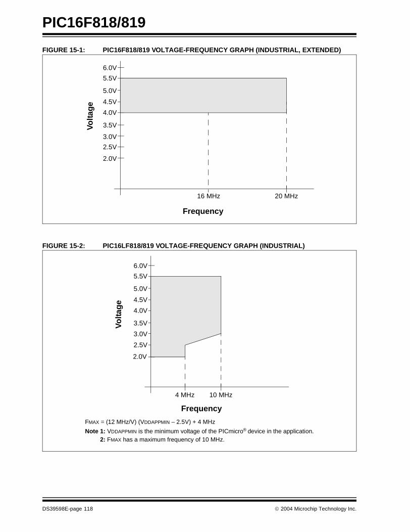
PIC16F818/819
FIGURE 15-1: PIC16F818/819 VOLTAGE-FREQUENCY GRAPH (INDUSTRIAL, EXTENDED)
FIGURE 15-2: PIC16LF818/819 VOLTAGE-FREQUENCY GRAPH (INDUSTRIAL)
Frequency
Volta
ge
6.0V
5.5V
4.5V
4.0V
2.0V
20 MHz
5.0V
3.5V
3.0V
2.5V
16 MHz
Frequency
Vo
ltag
e
6.0V
5.5V
4.5V
4.0V
2.0V
5.0V
3.5V
3.0V
2.5V
FMAX = (12 MHz/V) (VDDAPPMIN – 2.5V) + 4 MHz
Note 1: VDDAPPMIN is the minimum voltage of the PICmicro® device in the application.
4 MHz 10 MHz
Note 2: FMAX has a maximum frequency of 10 MHz.
DS39598E-page 118 2004 Microchip Technology Inc.

PIC16F818/819
15.1 DC Characteristics: Supply VoltagePIC16F818/819 (Industrial, Extended) PIC16LF818/819 (Industrial)
PIC16LF818/819 (Industrial)
Standard Operating Conditions (unless otherwise stated)Operating temperature -40°C ≤ TA ≤ +85°C for industrial
PIC16F818/819 (Industrial, Extended)
Standard Operating Conditions (unless otherwise stated)Operating temperature -40°C ≤ TA ≤ +85°C for industrial
-40°C ≤ TA ≤ +125°C for extended
Param No.
Symbol Characteristic Min Typ Max Units Conditions
VDD Supply Voltage
D001 PIC16LF818/819 2.0 — 5.5 V HS, XT, RC and LP Oscillator mode
D001 PIC16F818/819 4.0 — 5.5 V
D002 VDR RAM Data RetentionVoltage(1)
1.5 — — V
D003 VPOR VDD Start Voltage to ensure internal Power-on Reset signal
— — 0.7 V See Section 12.4 “Power-on Reset (POR)” for details
D004 SVDD VDD Rise Rateto ensure internal Power-on Reset signal
0.05 — — V/ms See Section 12.4 “Power-on Reset (POR)” for details
VBOR Brown-out Reset Voltage
D005 PIC16LF818/819 3.65 — 4.35 V
D005 PIC16F818/819 3.65 — 4.35 V FMAX = 14 MHz(2)
Legend: Shading of rows is to assist in readability of the table.Note 1: This is the limit to which VDD can be lowered in Sleep mode, or during a device Reset, without losing RAM data
2: When BOR is enabled, the device will operate correctly until the VBOR voltage trip point is reached.
2004 Microchip Technology Inc. DS39598E-page 119

PIC16F818/819
15.2 DC Characteristics: Power-Down and Supply CurrentPIC16F818/819 (Industrial, Extended) PIC16LF818/819 (Industrial)
PIC16LF818/819 (Industrial)
Standard Operating Conditions (unless otherwise stated)Operating temperature -40°C ≤ TA ≤ +85°C for industrial
PIC16F818/819 (Industrial, Extended)
Standard Operating Conditions (unless otherwise stated)Operating temperature -40°C ≤ TA ≤ +85°C for industrial
-40°C ≤ TA ≤ +125°C for extended
Param No.
Device Typ Max Units Conditions
Power-Down Current (IPD)(1)
PIC16LF818/819 0.1 0.4 µA -40°C
VDD = 2.0V0.1 0.4 µA +25°C
0.4 1.5 µA +85°C
PIC16LF818/819 0.3 0.5 µA -40°C
VDD = 3.0V0.3 0.5 µA +25°C
0.7 1.7 µA +85°C
All devices 0.6 1.0 µA -40°C
VDD = 5.0V0.6 1.0 µA +25°C
1.2 5.0 µA +85°C
Extended devices 6.0 28 µA +125°C
Legend: Shading of rows is to assist in readability of the table.Note 1: The power-down current in Sleep mode does not depend on the oscillator type. Power-down current is measured with
the part in Sleep mode, with all I/O pins in high-impedance state and tied to VDD or VSS and all features that add delta current disabled (such as WDT, Timer1 Oscillator, BOR, etc.).
2: The supply current is mainly a function of operating voltage, frequency and mode. Other factors, such as I/O pin loading and switching rate, oscillator type and circuit, internal code execution pattern and temperature, also have an impact on the current consumption.The test conditions for all IDD measurements in active operation mode are:
OSC1 = external square wave, from rail-to-rail; all I/O pins tri-stated, pulled to VDD;MCLR = VDD; WDT enabled/disabled as specified.
3: For RC oscillator configurations, current through REXT is not included. The current through the resistor can be estimated by the formula Ir = VDD/2REXT (mA) with REXT in kΩ.
DS39598E-page 120 2004 Microchip Technology Inc.

PIC16F818/819
Supply Current (IDD)(2,3)
PIC16LF818/819 9 20 µA -40°C
VDD = 2.0V
FOSC = 32 kHZ
(LP Oscillator)
7 15 µA +25°C
7 15 µA +85°C
PIC16LF818/819 16 30 µA -40°C
VDD = 3.0V14 25 µA +25°C
14 25 µA +85°C
All devices 32 40 µA -40°C
VDD = 5.0V26 35 µA +25°C
26 35 µA +85°C
Extended devices 35 53 µA +125°C
15.2 DC Characteristics: Power-Down and Supply CurrentPIC16F818/819 (Industrial, Extended) PIC16LF818/819 (Industrial) (Continued)
PIC16LF818/819 (Industrial)
Standard Operating Conditions (unless otherwise stated)Operating temperature -40°C ≤ TA ≤ +85°C for industrial
PIC16F818/819 (Industrial, Extended)
Standard Operating Conditions (unless otherwise stated)Operating temperature -40°C ≤ TA ≤ +85°C for industrial
-40°C ≤ TA ≤ +125°C for extended
Param No.
Device Typ Max Units Conditions
Legend: Shading of rows is to assist in readability of the table.Note 1: The power-down current in Sleep mode does not depend on the oscillator type. Power-down current is measured with
the part in Sleep mode, with all I/O pins in high-impedance state and tied to VDD or VSS and all features that add delta current disabled (such as WDT, Timer1 Oscillator, BOR, etc.).
2: The supply current is mainly a function of operating voltage, frequency and mode. Other factors, such as I/O pin loading and switching rate, oscillator type and circuit, internal code execution pattern and temperature, also have an impact on the current consumption.The test conditions for all IDD measurements in active operation mode are:
OSC1 = external square wave, from rail-to-rail; all I/O pins tri-stated, pulled to VDD;MCLR = VDD; WDT enabled/disabled as specified.
3: For RC oscillator configurations, current through REXT is not included. The current through the resistor can be estimated by the formula Ir = VDD/2REXT (mA) with REXT in kΩ.
2004 Microchip Technology Inc. DS39598E-page 121

PIC16F818/819
Supply Current (IDD)(2,3)
PIC16LF818/819 72 95 µA -40°C
VDD = 2.0V
FOSC = 1 MHZ
(RC Oscillator)(3)
76 90 µA +25°C
76 90 µA +85°C
PIC16LF818/819 138 175 µA -40°C
VDD = 3.0V136 170 µA +25°C
136 170 µA +85°C
All devices 310 380 µA -40°C
VDD = 5.0V290 360 µA +25°C
280 360 µA +85°C
Extended devices 350 500 µA +125°C
PIC16LF818/819 270 315 µA -40°C
VDD = 2.0V
FOSC = 4 MHz(RC Oscillator)(3)
280 310 µA +25°C
285 310 µA +85°C
PIC16LF818/819 460 610 µA -40°C
VDD = 3.0V450 600 µA +25°C
450 600 µA +85°C
All devices 900 1060 µA -40°C
VDD = 5.0V890 1050 µA +25°C
890 1050 µA +85°C
Extended devices .920 1.5 mA +125°C
15.2 DC Characteristics: Power-Down and Supply CurrentPIC16F818/819 (Industrial, Extended) PIC16LF818/819 (Industrial) (Continued)
PIC16LF818/819 (Industrial)
Standard Operating Conditions (unless otherwise stated)Operating temperature -40°C ≤ TA ≤ +85°C for industrial
PIC16F818/819 (Industrial, Extended)
Standard Operating Conditions (unless otherwise stated)Operating temperature -40°C ≤ TA ≤ +85°C for industrial
-40°C ≤ TA ≤ +125°C for extended
Param No.
Device Typ Max Units Conditions
Legend: Shading of rows is to assist in readability of the table.Note 1: The power-down current in Sleep mode does not depend on the oscillator type. Power-down current is measured with
the part in Sleep mode, with all I/O pins in high-impedance state and tied to VDD or VSS and all features that add delta current disabled (such as WDT, Timer1 Oscillator, BOR, etc.).
2: The supply current is mainly a function of operating voltage, frequency and mode. Other factors, such as I/O pin loading and switching rate, oscillator type and circuit, internal code execution pattern and temperature, also have an impact on the current consumption.The test conditions for all IDD measurements in active operation mode are:
OSC1 = external square wave, from rail-to-rail; all I/O pins tri-stated, pulled to VDD;MCLR = VDD; WDT enabled/disabled as specified.
3: For RC oscillator configurations, current through REXT is not included. The current through the resistor can be estimated by the formula Ir = VDD/2REXT (mA) with REXT in kΩ.
DS39598E-page 122 2004 Microchip Technology Inc.
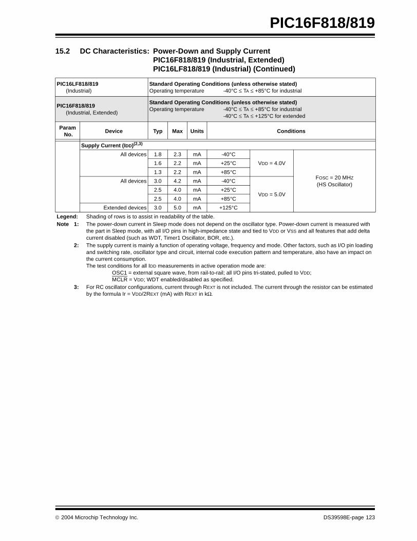
PIC16F818/819
Supply Current (IDD)(2,3)
All devices 1.8 2.3 mA -40°C
VDD = 4.0V
FOSC = 20 MHZ
(HS Oscillator)
1.6 2.2 mA +25°C
1.3 2.2 mA +85°C
All devices 3.0 4.2 mA -40°C
VDD = 5.0V2.5 4.0 mA +25°C
2.5 4.0 mA +85°C
Extended devices 3.0 5.0 mA +125°C
15.2 DC Characteristics: Power-Down and Supply CurrentPIC16F818/819 (Industrial, Extended) PIC16LF818/819 (Industrial) (Continued)
PIC16LF818/819 (Industrial)
Standard Operating Conditions (unless otherwise stated)Operating temperature -40°C ≤ TA ≤ +85°C for industrial
PIC16F818/819 (Industrial, Extended)
Standard Operating Conditions (unless otherwise stated)Operating temperature -40°C ≤ TA ≤ +85°C for industrial
-40°C ≤ TA ≤ +125°C for extended
Param No.
Device Typ Max Units Conditions
Legend: Shading of rows is to assist in readability of the table.Note 1: The power-down current in Sleep mode does not depend on the oscillator type. Power-down current is measured with
the part in Sleep mode, with all I/O pins in high-impedance state and tied to VDD or VSS and all features that add delta current disabled (such as WDT, Timer1 Oscillator, BOR, etc.).
2: The supply current is mainly a function of operating voltage, frequency and mode. Other factors, such as I/O pin loading and switching rate, oscillator type and circuit, internal code execution pattern and temperature, also have an impact on the current consumption.The test conditions for all IDD measurements in active operation mode are:
OSC1 = external square wave, from rail-to-rail; all I/O pins tri-stated, pulled to VDD;MCLR = VDD; WDT enabled/disabled as specified.
3: For RC oscillator configurations, current through REXT is not included. The current through the resistor can be estimated by the formula Ir = VDD/2REXT (mA) with REXT in kΩ.
2004 Microchip Technology Inc. DS39598E-page 123

PIC16F818/819
Supply Current (IDD)(2,3)
PIC16LF818/819 8 20 µA -40°C
VDD = 2.0V
FOSC = 31.25 kHz(RC_RUN mode,
Internal RC Oscillator)
7 15 µA +25°C
7 15 µA +85°C
PIC16LF818/819 16 30 µA -40°C
VDD = 3.0V14 25 µA +25°C
14 25 µA +85°C
All devices 32 40 µA -40°C
VDD = 5.0V29 35 µA +25°C
29 35 µA +85°C
Extended devices 35 45 µA +125°C
PIC16LF818/819 132 160 µA -40°C
VDD = 2.0V
FOSC = 1 MHz(RC_RUN mode,
Internal RC Oscillator)
126 155 µA +25°C
126 155 µA +85°C
PIC16LF818/819 260 310 µA -40°C
VDD = 3.0V230 300 µA +25°C
230 300 µA +85°C
All devices 560 690 µA -40°C
VDD = 5.0V500 650 µA +25°C
500 650 µA +85°C
Extended devices 570 710 µA +125°C
PIC16LF818/819 310 420 µA -40°C
VDD = 2.0V
FOSC = 4 MHz(RC_RUN mode,
Internal RC Oscillator)
300 410 µA +25°C
300 410 µA +85°C
PIC16LF818/819 550 650 µA -40°C
VDD = 3.0V530 620 µA +25°C
530 620 µA +85°C
All devices 1.2 1.5 mA -40°C
VDD = 5.0V1.1 1.4 mA +25°C
1.1 1.4 mA +85°C
Extended devices 1.3 1.6 mA +125°C
15.2 DC Characteristics: Power-Down and Supply CurrentPIC16F818/819 (Industrial, Extended) PIC16LF818/819 (Industrial) (Continued)
PIC16LF818/819 (Industrial)
Standard Operating Conditions (unless otherwise stated)Operating temperature -40°C ≤ TA ≤ +85°C for industrial
PIC16F818/819 (Industrial, Extended)
Standard Operating Conditions (unless otherwise stated)Operating temperature -40°C ≤ TA ≤ +85°C for industrial
-40°C ≤ TA ≤ +125°C for extended
Param No.
Device Typ Max Units Conditions
Legend: Shading of rows is to assist in readability of the table.Note 1: The power-down current in Sleep mode does not depend on the oscillator type. Power-down current is measured with
the part in Sleep mode, with all I/O pins in high-impedance state and tied to VDD or VSS and all features that add delta current disabled (such as WDT, Timer1 Oscillator, BOR, etc.).
2: The supply current is mainly a function of operating voltage, frequency and mode. Other factors, such as I/O pin loading and switching rate, oscillator type and circuit, internal code execution pattern and temperature, also have an impact on the current consumption.The test conditions for all IDD measurements in active operation mode are:
OSC1 = external square wave, from rail-to-rail; all I/O pins tri-stated, pulled to VDD;MCLR = VDD; WDT enabled/disabled as specified.
3: For RC oscillator configurations, current through REXT is not included. The current through the resistor can be estimated by the formula Ir = VDD/2REXT (mA) with REXT in kΩ.
DS39598E-page 124 2004 Microchip Technology Inc.

PIC16F818/819
Supply Current (IDD)(2,3)
PIC16LF818/819 .950 1.3 mA -40°C
VDD = 3.0V
FOSC = 8 MHz(RC_RUN mode,
Internal RC Oscillator)
.930 1.2 mA +25°C
.930 1.2 mA +85°C
All devices 1.8 3.0 mA -40°C
VDD = 5.0V1.7 2.8 mA +25°C
1.7 2.8 mA +85°C
Extended devices 2.0 4.0 mA +125°C
15.2 DC Characteristics: Power-Down and Supply CurrentPIC16F818/819 (Industrial, Extended) PIC16LF818/819 (Industrial) (Continued)
PIC16LF818/819 (Industrial)
Standard Operating Conditions (unless otherwise stated)Operating temperature -40°C ≤ TA ≤ +85°C for industrial
PIC16F818/819 (Industrial, Extended)
Standard Operating Conditions (unless otherwise stated)Operating temperature -40°C ≤ TA ≤ +85°C for industrial
-40°C ≤ TA ≤ +125°C for extended
Param No.
Device Typ Max Units Conditions
Legend: Shading of rows is to assist in readability of the table.Note 1: The power-down current in Sleep mode does not depend on the oscillator type. Power-down current is measured with
the part in Sleep mode, with all I/O pins in high-impedance state and tied to VDD or VSS and all features that add delta current disabled (such as WDT, Timer1 Oscillator, BOR, etc.).
2: The supply current is mainly a function of operating voltage, frequency and mode. Other factors, such as I/O pin loading and switching rate, oscillator type and circuit, internal code execution pattern and temperature, also have an impact on the current consumption.The test conditions for all IDD measurements in active operation mode are:
OSC1 = external square wave, from rail-to-rail; all I/O pins tri-stated, pulled to VDD;MCLR = VDD; WDT enabled/disabled as specified.
3: For RC oscillator configurations, current through REXT is not included. The current through the resistor can be estimated by the formula Ir = VDD/2REXT (mA) with REXT in kΩ.
2004 Microchip Technology Inc. DS39598E-page 125

PIC16F818/819
D022(∆IWDT)
Module Differential Currents (∆IWDT, ∆IBOR, ∆ILVD, ∆IOSCB, ∆IAD)
Watchdog Timer 1.5 3.8 µA -40°C
VDD = 2.0V2.2 3.8 µA +25°C
2.7 4.0 µA +85°C
2.3 4.6 µA -40°C
VDD = 3.0V2.7 4.6 µA +25°C
3.1 4.8 µA +85°C
3.0 10.0 µA -40°C
VDD = 5.0V3.3 10.0 µA +25°C
3.9 13.0 µA +85°C
Extended Devices 5.0 21.0 µA +125°C
D022A(∆IBOR)
Brown-out Reset 40 60 µA -40°C to +85°C VDD = 5.0V
D025(∆IOSCB)
Timer1 Oscillator 1.7 2.3 µA -40°C
VDD = 2.0V
32 kHz on Timer1
1.8 2.3 µA +25°C
2.0 2.3 µA +85°C
2.2 3.8 µA -40°C
VDD = 3.0V2.6 3.8 µA +25°C
2.9 3.8 µA +85°C
3.0 6.0 µA -40°C
VDD = 5.0V3.2 6.0 µA +25°C
3.4 7.0 µA +85°C
D026(∆IAD)
A/D Converter 0.001 2.0 µA -40°C to +85°C VDD = 2.0V
A/D on, Sleep, not converting0.001 2.0 µA -40°C to +85°C VDD = 3.0V
0.003 2.0 µA -40°C to +85°CVDD = 5.0V
Extended Devices 4.0 8.0 µA -40°C to +125°C
15.2 DC Characteristics: Power-Down and Supply CurrentPIC16F818/819 (Industrial, Extended) PIC16LF818/819 (Industrial) (Continued)
PIC16LF818/819 (Industrial)
Standard Operating Conditions (unless otherwise stated)Operating temperature -40°C ≤ TA ≤ +85°C for industrial
PIC16F818/819 (Industrial, Extended)
Standard Operating Conditions (unless otherwise stated)Operating temperature -40°C ≤ TA ≤ +85°C for industrial
-40°C ≤ TA ≤ +125°C for extended
Param No.
Device Typ Max Units Conditions
Legend: Shading of rows is to assist in readability of the table.Note 1: The power-down current in Sleep mode does not depend on the oscillator type. Power-down current is measured with
the part in Sleep mode, with all I/O pins in high-impedance state and tied to VDD or VSS and all features that add delta current disabled (such as WDT, Timer1 Oscillator, BOR, etc.).
2: The supply current is mainly a function of operating voltage, frequency and mode. Other factors, such as I/O pin loading and switching rate, oscillator type and circuit, internal code execution pattern and temperature, also have an impact on the current consumption.The test conditions for all IDD measurements in active operation mode are:
OSC1 = external square wave, from rail-to-rail; all I/O pins tri-stated, pulled to VDD;MCLR = VDD; WDT enabled/disabled as specified.
3: For RC oscillator configurations, current through REXT is not included. The current through the resistor can be estimated by the formula Ir = VDD/2REXT (mA) with REXT in kΩ.
DS39598E-page 126 2004 Microchip Technology Inc.

PIC16F818/819
15.3 DC Characteristics: Internal RC AccuracyPIC16F818/819, PIC16F818/819 TSL (Industrial, Extended)PIC16LF818/819, PIC16LF818/819 TSL (Industrial)
PIC16LF818/819(3)
PIC16LF818/819 TSL(3)
(Industrial)
Standard Operating Conditions (unless otherwise stated)Operating temperature -40°C ≤ TA ≤ +85°C for industrial
PIC16F818/819(3)
PIC16F818/819 TSL(3)
(Industrial, Extended)
Standard Operating Conditions (unless otherwise stated)Operating temperature -40°C ≤ TA ≤ +85°C for industrial
-40°C ≤ TA ≤ +125°C for extended
ParamNo.
Device Min Typ Max Units Conditions
INTOSC Accuracy @ Freq = 8 MHz, 4 MHz, 2 MHz, 1 MHz, 500 kHz, 250 kHz, 125 kHz(1)
PIC16LF818/819 -5 ±1 5 % +25°C
VDD = 2.7-3.3V-25 — 25 % -10°C to +85°C
-30 — 30 % -40°C to +85°C
PIC16F818/819(4) -5 ±1 5 % +25°C
VDD = 4.5-5.5V-25 — 25 % -10°C to +85°C
-30 — 30 % -40°C to +85°C
-35 — 35 % -40°C to +125°C
PIC16LF818/819 TSL -2 ±1 2 % +25°C
VDD = 2.7-3.3V-5 — 5 % -10°C to +85°C
-10 — 10 % -40°C to +85°C
PIC16F818/819 TSL(5) -2 ±1 2 % +25°C
VDD = 4.5-5.5V-5 — 5 % -10°C to +85°C
-10 — 10 % -40°C to +85°C
-15 — 15 % -40°C to +125°C
INTRC Accuracy @ Freq = 31 kHz(2)
PIC16LF818/819 26.562 — 35.938 kHz -40°C to +85°C VDD = 2.7-3.3V
PIC16F818/819(4) 26.562 — 35.938 kHz -40°C to +85°C VDD = 4.5-5.5V
PIC16LF818/819 TSL 26.562 — 35.938 kHz -40°C to +85°C VDD = 2.7-3.3V
PIC16F818/819 TSL(5) 26.562 — 35.938 kHz -40°C to +85°C VDD = 4.5-5.5V
Legend: Shading of rows is to assist in readability of the table.Note 1: Frequency calibrated at 25°C. OSCTUNE register can be used to compensate for temperature drift.
2: INTRC frequency after calibration.3: The only specification difference between a non-TSL device and a TSL device is the internal RC oscillator specifications
listed above. All other specifications are maintained.4: Example part number for the specifications listed above: PIC16F818-I/SS (PIC16F818 device, Industrial temperature,
SSOP package).5: Example part number for the specifications listed above: PIC16F818-I/SSTSL (PIC16F818 device, Industrial
temperature, SSOP package).
2004 Microchip Technology Inc. DS39598E-page 127

PIC16F818/819
15.4 DC Characteristics: PIC16F818/819 (Industrial, Extended)PIC16LF818/819 (Industrial)
DC CHARACTERISTICS
Standard Operating Conditions (unless otherwise stated)Operating temperature -40°C ≤ TA ≤ +85°C for industrial
-40°C ≤ TA ≤ +125°C for extendedOperating voltage VDD range as described in Section 15.1 “DC Characteristics: Supply Voltage”.
ParamNo.
Sym Characteristic Min Typ† Max Units Conditions
VIL Input Low Voltage
I/O ports:
D030 with TTL buffer VSS — 0.15 VDD V For entire VDD range
D030A VSS — 0.8V V 4.5V ≤ VDD ≤ 5.5V
D031 with Schmitt Trigger buffer VSS — 0.2 VDD V
D032 MCLR, OSC1 (in RC mode) VSS — 0.2 VDD V (Note 1)
D033 OSC1 (in XT and LP mode) VSS — 0.3V V
OSC1 (in HS mode) VSS — 0.3 VDD V
Ports RB1 and RB4:
D034 with Schmitt Trigger buffer VSS — 0.3 VDD V For entire VDD range
VIH Input High Voltage
I/O ports:
D040 with TTL buffer 2.0 — VDD V 4.5V ≤ VDD ≤ 5.5V
D040A 0.25 VDD + 0.8V — VDD V For entire VDD range
D041 with Schmitt Trigger buffer 0.8 VDD — VDD V For entire VDD range
D042 MCLR 0.8 VDD — VDD V
D042A OSC1 (in XT and LP mode) 1.6V — VDD V
OSC1 (in HS mode) 0.7 VDD — VDD V
D043 OSC1 (in RC mode) 0.9 VDD — VDD V (Note 1)
Ports RB1 and RB4:
D044 with Schmitt Trigger buffer 0.7 VDD — VDD V For entire VDD range
D070 IPURB PORTB Weak Pull-up Current 50 250 400 µA VDD = 5V, VPIN = VSS
IIL Input Leakage Current (Notes 2, 3)
D060 I/O ports — — ±1 µA Vss ≤ VPIN ≤ VDD, pin at high-impedance
D061 MCLR — — ±5 µA Vss ≤ VPIN ≤ VDD
D063 OSC1 — — ±5 µA Vss ≤ VPIN ≤ VDD, XT, HS and LP oscillator configuration
† Data in “Typ” column is at 5V, 25°C unless otherwise stated. These parameters are for design guidance only and are not tested.
Note 1: In RC oscillator configuration, the OSC1/CLKI pin is a Schmitt Trigger input. It is not recommended that the PIC16F818/819 be driven with external clock in RC mode.
2: The leakage current on the MCLR pin is strongly dependent on the applied voltage level. The specified levels represent normal operating conditions. Higher leakage current may be measured at different input voltages.
3: Negative current is defined as current sourced by the pin.
DS39598E-page 128 2004 Microchip Technology Inc.

PIC16F818/819
VOL Output Low Voltage
D080 I/O ports — — 0.6 V IOL = 8.5 mA, VDD = 4.5V, -40°C to +125°C
D083 OSC2/CLKO (RC oscillator config)
— — 0.6 V IOL = 1.6 mA, VDD = 4.5V, -40°C to +125°C
VOH Output High Voltage
D090 I/O ports (Note 3) VDD – 0.7 — — V IOH = -3.0 mA, VDD = 4.5V, -40°C to +125°C
D092 OSC2/CLKO (RC oscillator config)
VDD – 0.7 — — V IOH = -1.3 mA, VDD = 4.5V, -40°C to +125°C
Capacitive Loading Specs on Output Pins
D100 COSC2 OSC2 pin — — 15 pF In XT, HS and LP modes when external clock is used to drive OSC1
D101 CIO All I/O pins and OSC2(in RC mode)
— — 50 pF
D102 CB SCL, SDA in I2C™ mode — — 400 pF
Data EEPROM Memory
D120 ED Endurance 100K
10K
1M
100K
—
—
E/W
E/W
-40°C to +85°C
+85°C to +125°C
D121 VDRW VDD for read/write VMIN — 5.5 V Using EECON to read/write, VMIN = min. operating voltage
D122 TDEW Erase/write cycle time — 4 8 ms
Program Flash Memory
D130 EP Endurance 10K1K
100K10K
——
E/WE/W
-40°C to +85°C+85°C to +125°C
D131 VPR VDD for read VMIN — 5.5 V
D132A VDD for erase/write VMIN — 5.5 V Using EECON to read/write, VMIN = min. operating voltage
D133 TPE Erase cycle time — 2 4 ms
D134 TPW Write cycle time — 2 4 ms
15.4 DC Characteristics: PIC16F818/819 (Industrial, Extended)PIC16LF818/819 (Industrial) (Continued)
DC CHARACTERISTICS
Standard Operating Conditions (unless otherwise stated)Operating temperature -40°C ≤ TA ≤ +85°C for industrial
-40°C ≤ TA ≤ +125°C for extendedOperating voltage VDD range as described in Section 15.1 “DC Characteristics: Supply Voltage”.
ParamNo.
Sym Characteristic Min Typ† Max Units Conditions
† Data in “Typ” column is at 5V, 25°C unless otherwise stated. These parameters are for design guidance only and are not tested.
Note 1: In RC oscillator configuration, the OSC1/CLKI pin is a Schmitt Trigger input. It is not recommended that the PIC16F818/819 be driven with external clock in RC mode.
2: The leakage current on the MCLR pin is strongly dependent on the applied voltage level. The specified levels represent normal operating conditions. Higher leakage current may be measured at different input voltages.
3: Negative current is defined as current sourced by the pin.
2004 Microchip Technology Inc. DS39598E-page 129
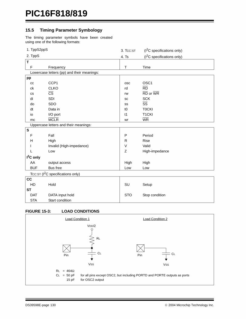
PIC16F818/819
15.5 Timing Parameter Symbology
The timing parameter symbols have been createdusing one of the following formats:
FIGURE 15-3: LOAD CONDITIONS
1. TppS2ppS 3. TCC:ST (I2C specifications only)
2. TppS 4. Ts (I2C specifications only)T
F Frequency T Time
Lowercase letters (pp) and their meanings:pp
cc CCP1 osc OSC1
ck CLKO rd RDcs CS rw RD or WRdi SDI sc SCK
do SDO ss SSdt Data in t0 T0CKIio I/O port t1 T1CKI
mc MCLR wr WRUppercase letters and their meanings:
SF Fall P PeriodH High R RiseI Invalid (High-impedance) V Valid
L Low Z High-impedance
I2C onlyAA output access High High
BUF Bus free Low Low
TCC:ST (I2C specifications only)CC
HD Hold SU SetupST
DAT DATA input hold STO Stop condition
STA Start condition
VDD/2
CL
RL
Pin Pin
VSS VSS
CL
RL = 464ΩCL = 50 pF for all pins except OSC2, but including PORTD and PORTE outputs as ports
15 pF for OSC2 output
Load Condition 1 Load Condition 2
DS39598E-page 130 2004 Microchip Technology Inc.

PIC16F818/819
FIGURE 15-4: EXTERNAL CLOCK TIMING
OSC1
CLKO
Q4 Q1 Q2 Q3 Q4 Q1
1
2
3 3 4 4
TABLE 15-1: EXTERNAL CLOCK TIMING REQUIREMENTS
Param No.
Sym Characteristic Min Typ† Max Units Conditions
FOSC External CLKI Frequency (Note 1) DC — 1 MHz XT and RC Oscillator mode
DC — 20 MHz HS Oscillator mode
DC — 32 kHz LP Oscillator mode
Oscillator Frequency (Note 1) DC — 4 MHz RC Oscillator mode
0.1 — 4 MHz XT Oscillator mode
4
5
—
—
20
200
MHz
kHz
HS Oscillator mode
LP Oscillator mode
1 TOSC External CLKI Period (Note 1) 1000 — — ns XT and RC Oscillator mode
50 — — ns HS Oscillator mode
5 — — ms LP Oscillator mode
Oscillator Period (Note 1) 250 — — ns RC Oscillator mode
250 — 10,000 ns XT Oscillator mode
50 — 250 ns HS Oscillator mode
5 — — ms LP Oscillator mode
2 TCY Instruction Cycle Time (Note 1) 200 TCY DC ns TCY = 4/FOSC
3 TOSL,TOSH
External Clock in (OSC1) High or Low Time
500 — — ns XT Oscillator
2.5 — — ms LP Oscillator
15 — — ns HS Oscillator
4 TOSR,TOSF
External Clock in (OSC1) Rise or Fall Time
— — 25 ns XT Oscillator
— — 50 ns LP Oscillator
— — 15 ns HS Oscillator
† Data in “Typ” column is at 5V, 25°C unless otherwise stated. These parameters are for design guidanceonly and are not tested.
Note 1: Instruction cycle period (TCY) equals four times the input oscillator time base period. All specified values are based on characterization data for that particular oscillator type, under standard operating conditions, with the device executing code. Exceeding these specified limits may result in an unstable oscillator operation and/or higher than expected current consumption. All devices are tested to operate at “min.” values with an external clock applied to the OSC1/CLKI pin. When an external clock input is used, the “max.” cycle time limit is “DC” (no clock) for all devices.
2004 Microchip Technology Inc. DS39598E-page 131

PIC16F818/819
FIGURE 15-5: CLKO AND I/O TIMING
TABLE 15-2: CLKO AND I/O TIMING REQUIREMENTS
Note: Refer to Figure 15-3 for load conditions.
OSC1
CLKO
I/O pin(Input)
I/O pin(Output)
Q4 Q1 Q2 Q3
10
1314
17
20, 21
19 18
15
11
1216
Old Value New Value
ParamNo.
Symbol Characteristic Min Typ† Max Units Conditions
10* TOSH2CKL OSC1 ↑ to CLKO ↓ — 75 200 ns (Note 1)
11* TOSH2CKH OSC1 ↑ to CLKO ↑ — 75 200 ns (Note 1)
12* TCKR CLKO Rise Time — 35 100 ns (Note 1)
13* TCKF CLKO Fall Time — 35 100 ns (Note 1)
14* TCKL2IOV CLKO ↓ to Port Out Valid — — 0.5 TCY + 20 ns (Note 1)
15* TIOV2CKH Port In Valid before CLKO ↑ TOSC + 200 — — ns (Note 1)
16* TCKH2IOI Port In Hold after CLKO ↑ 0 — — ns (Note 1)
17* TOSH2IOV OSC1 ↑ (Q1 cycle) to Port Out Valid — 100 255 ns
18* TOSH2IOI OSC1 ↑ (Q2 cycle) to Port Input Invalid (I/O in hold time)
PIC16F818/819 100 — — ns
PIC16LF818/819 200 — — ns
19* TIOV2OSH Port Input Valid to OSC1 ↑ (I/O in setup time) 0 — — ns
20* TIOR Port Output Rise Time PIC16F818/819 — 10 40 ns
PIC16LF818/819 — — 145 ns
21* TIOF Port Output Fall Time PIC16F818/819 — 10 40 ns
PIC16LF818/819 — — 145 ns
22††* TINP INT pin High or Low Time TCY — — ns
23††* TRBP RB7:RB4 Change INT High or Low Time TCY — — ns
* These parameters are characterized but not tested.† Data in “Typ” column is at 5V, 25°C unless otherwise stated. These parameters are for design guidance only and are not
tested.†† These parameters are asynchronous events, not related to any internal clock edges.
Note 1: Measurements are taken in RC mode, where CLKO output is 4 x TOSC.
DS39598E-page 132 2004 Microchip Technology Inc.

PIC16F818/819
FIGURE 15-6: RESET, WATCHDOG TIMER, OSCILLATOR START-UP TIMER AND POWER-UP TIMER TIMING
FIGURE 15-7: BROWN-OUT RESET TIMING
TABLE 15-3: RESET, WATCHDOG TIMER, OSCILLATOR START-UP TIMER, POWER-UP TIMER AND BROWN-OUT RESET REQUIREMENTS
VDD
MCLR
InternalPOR
PWRTTime-out
OscillatorTime-out
InternalReset
WatchdogTimerReset
33
32
30
3134
I/O pins
34
Note: Refer to Figure 15-3 for load conditions.
VDD VBOR
35
Param No.
Symbol Characteristic Min Typ† Max Units Conditions
30 TMCL MCLR Pulse Width (Low) 2 — — µs VDD = 5V, -40°C to +85°C
31* TWDT Watchdog Timer Time-out Period (no prescaler)
13.6 16 18.4 ms VDD = 5V, -40°C to +85°C
32 TOST Oscillation Start-up Timer Period — 1024 TOSC — — TOSC = OSC1 period
33* TPWRT Power-up Timer Period 61.2 72 82.8 ms VDD = 5V, -40°C to +85°C
34 TIOZ I/O High-Impedance from MCLR Low or Watchdog Timer Reset
— — 2.1 µs
35 TBOR Brown-out Reset Pulse Width 100 — — µs VDD ≤ VBOR (D005)
* These parameters are characterized but not tested.† Data in “Typ” column is at 5V, 25°C unless otherwise stated. These parameters are for design guidance only and are not
tested.
2004 Microchip Technology Inc. DS39598E-page 133

PIC16F818/819
FIGURE 15-8: TIMER0 AND TIMER1 EXTERNAL CLOCK TIMINGS
TABLE 15-4: TIMER0 AND TIMER1 EXTERNAL CLOCK REQUIREMENTSParam
No.Symbol Characteristic Min Typ† Max Units Conditions
40* TT0H T0CKI High Pulse Width No Prescaler 0.5 TCY + 20 — — ns Must also meet parameter 42 With Prescaler 10 — — ns
41* TT0L T0CKI Low Pulse Width No Prescaler 0.5 TCY + 20 — — ns Must also meet parameter 42 With Prescaler 10 — — ns
42* TT0P T0CKI Period No Prescaler TCY + 40 — — ns
With Prescaler Greater of:20 or TCY + 40
N
— — ns N = prescale value (2, 4, ..., 256)
45* TT1H T1CKI High Time
Synchronous, Prescaler = 1 0.5 TCY + 20 — — ns Must also meet parameter 47 Synchronous,
Prescaler = 2,4,8PIC16F818/819 15 — — ns
PIC16LF818/819 25 — — ns
Asynchronous PIC16F818/819 30 — — ns
PIC16LF818/819 50 — — ns
46* TT1L T1CKI Low Time Synchronous, Prescaler = 1 0.5 TCY + 20 — — ns Must also meet parameter 47 Synchronous,
Prescaler = 2,4,8PIC16F818/819 15 — — ns
PIC16LF818/819 25 — — ns
Asynchronous PIC16F818/819 30 — — ns
PIC16LF818/819 50 — — ns
47* TT1P T1CKI Input Period
Synchronous PIC16F818/819 Greater of:30 or TCY + 40
N
— — ns N = prescale value (1, 2, 4, 8)
PIC16LF818/819 Greater of:50 or TCY + 40
N
N = prescale value (1, 2, 4, 8)
Asynchronous PIC16F818/819 60 — — ns
PIC16LF818/819 100 — — ns
FT1 Timer1 Oscillator Input Frequency Range (Oscillator enabled by setting bit T1OSCEN)
DC — 32.768 kHz
48 TCKEZTMR1 Delay from External Clock Edge to Timer Increment 2 TOSC — 7 TOSC —
* These parameters are characterized but not tested.† Data in “Typ” column is at 5V, 25°C unless otherwise stated. These parameters are for design guidance only and are not tested.
Note: Refer to Figure 15-3 for load conditions.
46
47
45
48
41
42
40
RA4/T0CKI
RB6/T1OSO/T1CKI
TMR0 or TMR1
DS39598E-page 134 2004 Microchip Technology Inc.

PIC16F818/819
FIGURE 15-9: CAPTURE/COMPARE/PWM TIMINGS (CCP1)
TABLE 15-5: CAPTURE/COMPARE/PWM REQUIREMENTS (CCP1)
Note: Refer to Figure 15-3 for load conditions.
CCP1(Capture Mode)
50 51
52
53 54
CCP1(Compare or PWM Mode)
Param No.
Symbol Characteristic Min Typ† Max Units Conditions
50* TCCL CCP1Input Low Time
No Prescaler 0.5 TCY + 20 — — ns
PIC16F818/819 10 — — ns
With Prescaler PIC16LF818/819 20 — — ns
51* TCCH CCP1Input High Time
No Prescaler 0.5 TCY + 20 — — ns
PIC16F818/819 10 — — ns
With Prescaler PIC16LF818/819 20 — — ns
52* TCCP CCP1 Input Period 3 TCY + 40N
— — ns N = prescale value (1,4 or 16)
53* TCCR CCP1 Output Rise Time PIC16F818/819 — 10 25 ns
PIC16LF818/819 — 25 50 ns
54* TCCF CCP1 Output Fall Time PIC16F818/819 — 10 25 ns
PIC16LF818/819 — 25 45 ns
* These parameters are characterized but not tested.† Data in “Typ” column is at 5V, 25°C unless otherwise stated. These parameters are for design guidance
only and are not tested.
2004 Microchip Technology Inc. DS39598E-page 135

PIC16F818/819
FIGURE 15-10: SPI™ MASTER MODE TIMING (CKE = 0, SMP = 0)
FIGURE 15-11: SPI™ MASTER MODE TIMING (CKE = 1, SMP = 1)
SS
SCK(CKP = 0)
SCK(CKP = 1)
SDO
SDI
70
71 72
7374
75, 76
787980
7978
MSb LSbBit 6 - - - - - -1
LSb InBit 6 - - - -1
Note: Refer to Figure 15-3 for load conditions.
MSb In
SS
SCK(CKP = 0)
SCK(CKP = 1)
SDO
SDI
81
71 72
74
75, 76
78
80
MSb
7973
MSb In
Bit 6 - - - - - -1
LSb InBit 6 - - - -1
LSb
Note: Refer to Figure 15-3 for load conditions.
DS39598E-page 136 2004 Microchip Technology Inc.
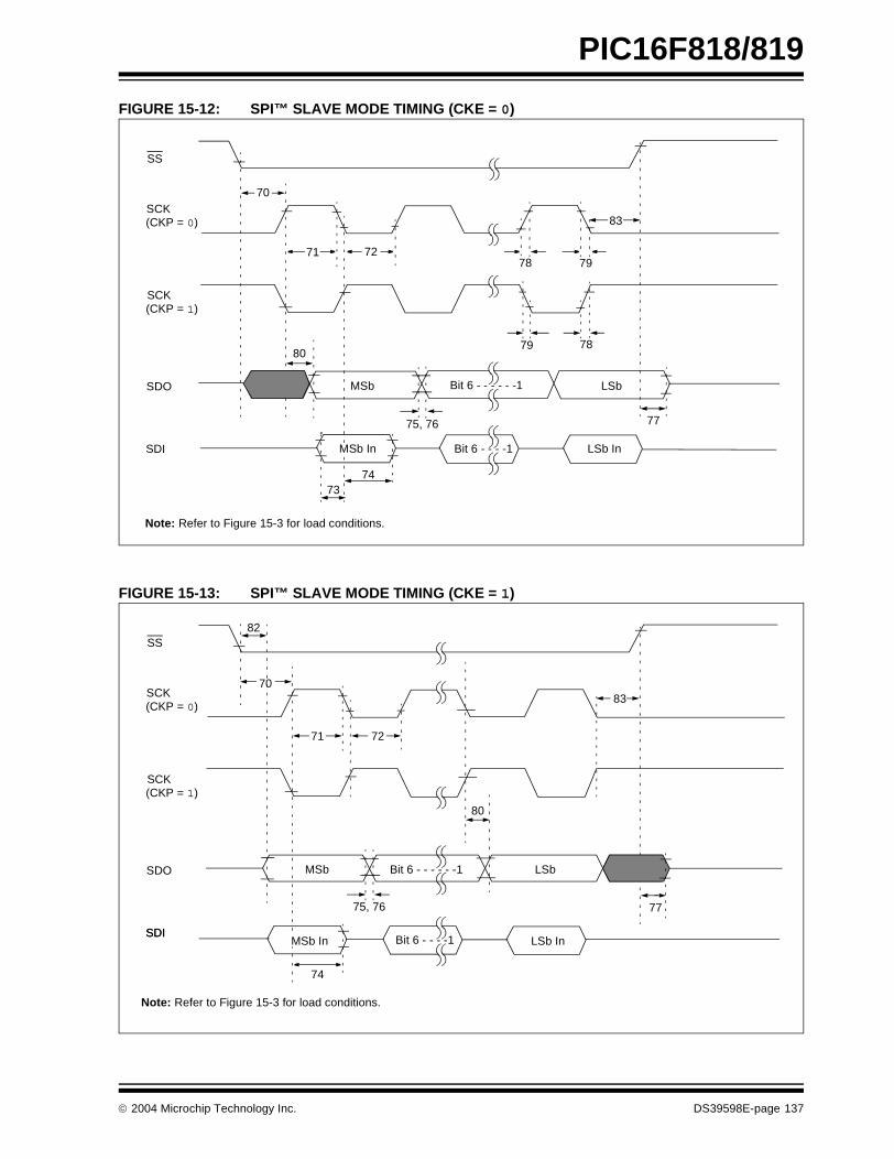
PIC16F818/819
FIGURE 15-12: SPI™ SLAVE MODE TIMING (CKE = 0)
FIGURE 15-13: SPI™ SLAVE MODE TIMING (CKE = 1)
SS
SCK(CKP = 0)
SCK(CKP = 1)
SDO
SDI
70
71 72
7374
75, 76 77
787980
7978
MSb LSbBit 6 - - - - - -1
Bit 6 - - - -1 LSb In
83
Note: Refer to Figure 15-3 for load conditions.
MSb In
SS
SCK(CKP = 0)
SCK(CKP = 1)
SDO
SDI
70
71 72
82
SDI
74
75, 76
MSb Bit 6 - - - - - -1 LSb
77
Bit 6 - - - -1 LSb In
80
83
Note: Refer to Figure 15-3 for load conditions.
MSb In
2004 Microchip Technology Inc. DS39598E-page 137

PIC16F818/819
TABLE 15-6: SPI™ MODE REQUIREMENTS
FIGURE 15-14: I2C™ BUS START/STOP BITS TIMING
Param No.
Symbol Characteristic Min Typ† Max Units Conditions
70* TSSL2SCH, TSSL2SCL
SS ↓ to SCK ↓ or SCK ↑ Input TCY — — ns
71* TSCH SCK Input High Time (Slave mode) TCY + 20 — — ns
72* TSCL SCK Input Low Time (Slave mode) TCY + 20 — — ns
73* TDIV2SCH, TDIV2SCL
Setup Time of SDI Data Input to SCK Edge 100 — — ns
74* TSCH2DIL, TSCL2DIL
Hold Time of SDI Data Input to SCK Edge 100 — — ns
75* TDOR SDO Data Output Rise Time PIC16F818/819PIC16LF818/819
——
1025
2550
nsns
76* TDOF SDO Data Output Fall Time — 10 25 ns
77* TSSH2DOZ SS ↑ to SDO Output High-Impedance 10 — 50 ns
78* TSCR SCK Output Rise Time (Master mode)
PIC16F818/819PIC16LF818/819
——
1025
2550
nsns
79* TSCF SCK Output Fall Time (Master mode) — 10 25 ns
80* TSCH2DOV,TSCL2DOV
SDO Data Output Valid after SCK Edge
PIC16F818/819PIC16LF818/819
——
——
50145
nsns
81* TDOV2SCH,TDOV2SCL
SDO Data Output Setup to SCK Edge TCY — — ns
82* TSSL2DOV SDO Data Output Valid after SS ↓ Edge — — 50 ns
83* TSCH2SSH,TSCL2SSH
SS ↑ after SCK Edge 1.5 TCY + 40 — — ns
* These parameters are characterized but not tested.† Data in “Typ” column is at 5V, 25°C unless otherwise stated. These parameters are for design guidance only and are not
tested.
Note: Refer to Figure 15-3 for load conditions.
91
92
93SCL
SDA
StartCondition
StopCondition
90
DS39598E-page 138 2004 Microchip Technology Inc.

PIC16F818/819
TABLE 15-7: I2C™ BUS START/STOP BITS REQUIREMENTS
FIGURE 15-15: I2C™ BUS DATA TIMING
ParamNo.
Symbol Characteristic Min Typ Max Units Conditions
90* TSU:STA Start Condition 100 kHz mode 4700 — — ns Only relevant for Repeated Start conditionSetup Time 400 kHz mode 600 — —
91* THD:STA Start Condition 100 kHz mode 4000 — — ns After this period, the first clock pulse is generatedHold Time 400 kHz mode 600 — —
92* TSU:STO Stop Condition 100 kHz mode 4700 — — ns
Setup Time 400 kHz mode 600 — —
93 THD:STO Stop Condition 100 kHz mode 4000 — — ns
Hold Time 400 kHz mode 600 — —
* These parameters are characterized but not tested.
Note: Refer to Figure 15-3 for load conditions.
90
91 92
100
101
103
106 107
109 109110
102
SCL
SDAIn
SDAOut
2004 Microchip Technology Inc. DS39598E-page 139

PIC16F818/819
TABLE 15-8: I2C™ BUS DATA REQUIREMENTS
Param.No.
Symbol Characteristic Min Max Units Conditions
100* THIGH Clock High Time 100 kHz mode 4.0 — µs
400 kHz mode 0.6 — µs
SSP Module 1.5 TCY —
101* TLOW Clock Low Time 100 kHz mode 4.7 — µs
400 kHz mode 1.3 — µs
SSP Module 1.5 TCY —
102* TR SDA and SCL Rise Time
100 kHz mode — 1000 ns
400 kHz mode 20 + 0.1 CB 300 ns CB is specified to be from 10-400 pF
103* TF SDA and SCL Fall Time
100 kHz mode — 300 ns
400 kHz mode 20 + 0.1 CB 300 ns CB is specified to be from 10-400 pF
90* TSU:STA Start Condition Setup Time
100 kHz mode 4.7 — µs Only relevant for Repeated Start condition400 kHz mode 0.6 — µs
91* THD:STA Start Condition Hold Time
100 kHz mode 4.0 — µs After this period, the first clock pulse is generated400 kHz mode 0.6 — µs
106* THD:DAT Data Input Hold Time
100 kHz mode 0 — ns
400 kHz mode 0 0.9 µs
107* TSU:DAT Data Input Setup Time
100 kHz mode 250 — ns (Note 2)
400 kHz mode 100 — ns
92* TSU:STO Stop Condition Setup Time
100 kHz mode 4.7 — µs
400 kHz mode 0.6 — µs
109* TAA Output Valid from Clock
100 kHz mode — 3500 ns (Note 1)
400 kHz mode — — ns
110* TBUF Bus Free Time 100 kHz mode 4.7 — µs Time the bus must be free before a new transmission can start
400 kHz mode 1.3 — µs
CB Bus Capacitive Loading — 400 pF
* These parameters are characterized but not tested.Note 1: As a transmitter, the device must provide this internal minimum delay time to bridge the undefined region
(min. 300 ns) of the falling edge of SCL to avoid unintended generation of Start or Stop conditions.2: A Fast mode (400 kHz) I2C™ bus device can be used in a Standard mode (100 kHz) I2C bus system but
the requirement, TSU:DAT ≥ 250 ns, must then be met. This will automatically be the case if the device does not stretch the LOW period of the SCL signal. If such a device does stretch the LOW period of the SCL signal, it must output the next data bit to the SDA line, TR max. + TSU:DAT = 1000 + 250 = 1250 ns (according to the Standard mode I2C bus specification), before the SCL line is released.
DS39598E-page 140 2004 Microchip Technology Inc.

PIC16F818/819
TABLE 15-9: A/D CONVERTER CHARACTERISTICS: PIC16F818/819 (INDUSTRIAL, EXTENDED)PIC16LF818/819 (INDUSTRIAL)
ParamNo.
Sym Characteristic Min Typ† Max Units Conditions
A01 NR Resolution — — 10-bits bit VREF = VDD = 5.12V, VSS ≤ VAIN ≤ VREF
A03 EIL Integral Linearity Error — — <±1 LSb VREF = VDD = 5.12V, VSS ≤ VAIN ≤ VREF
A04 EDL Differential Linearity Error — — <±1 LSb VREF = VDD = 5.12V, VSS ≤ VAIN ≤ VREF
A06 EOFF Offset Error — — <±2 LSb VREF = VDD = 5.12V, VSS ≤ VAIN ≤ VREF
A07 EGN Gain Error — — <±1 LSb VREF = VDD = 5.12V, VSS ≤ VAIN ≤ VREF
A10 — Monotonicity — guaranteed(3) — — VSS ≤ VAIN ≤ VREF
A20 VREF Reference Voltage (VREF+ – VREF-) 2.0 — VDD + 0.3 V
A21 VREF+ Reference Voltage High AVDD – 2.5V AVDD + 0.3V V
A22 VREF- Reference Voltage Low AVSS – 0.3V VREF+ – 2.0V V
A25 VAIN Analog Input Voltage VSS – 0.3V — VREF + 0.3V V
A30 ZAIN Recommended Impedance of Analog Voltage Source
— — 2.5 kΩ (Note 4)
A40 IAD A/D Conversion Current (VDD)
PIC16F818/819 — 220 — µA Average current consumption when A/D is on (Note 1)
PIC16LF818/819 — 90 — µA
A50 IREF VREF Input Current (Note 2) —
—
—
—
5
150
µA
µA
During VAIN acquisition.Based on differential of VHOLD to VAIN to charge CHOLD, see Section 11.1 “A/D Acquisition Requirements”.During A/D conversion cycle
† Data in “Typ” column is at 5V, 25°C unless otherwise stated. These parameters are for design guidance only and are not tested.
Note 1: When A/D is off, it will not consume any current other than minor leakage current. The power-down current spec includes any such leakage from the A/D module.
2: VREF current is from RA3 pin or VDD pin, whichever is selected as reference input.3: The A/D conversion result never decreases with an increase in the input voltage and has no missing codes.4: Maximum allowed impedance for analog voltage source is 10 kΩ. This requires higher acquisition time.
2004 Microchip Technology Inc. DS39598E-page 141

PIC16F818/819
FIGURE 15-16: A/D CONVERSION TIMING
TABLE 15-10: A/D CONVERSION REQUIREMENTS
131
130
132
BSF ADCON0, GO
Q4
A/D CLK
A/D DATA
ADRES
ADIF
GO
SAMPLE
OLD_DATA
Sampling Stopped
DONE
NEW_DATA
(TOSC/2)(1)
9 8 7 2 1 0
Note: If the A/D clock source is selected as RC, a time of TCY is added before the A/D clock starts. This allows the SLEEPinstruction to be executed.
1 TCY
. . . . . .
Param No.
Symbol Characteristic Min Typ† Max Units Conditions
130 TAD A/D Clock Period PIC16F818/819 1.6 — — µs TOSC based, VREF ≥ 3.0V
PIC16LF818/819 3.0 — — µs TOSC based, VREF ≥ 2.0V
PIC16F818/819 2.0 4.0 6.0 µs A/D RC mode
PIC16LF818/819 3.0 6.0 9.0 µs A/D RC mode
131 TCNV Conversion Time (not including S/H time) (Note 1)
— 12 TAD
132 TACQ Acquisition Time (Note 2)
10*
40
—
—
—
µs
µs The minimum time is the amplifier settling time. This may be used if the “new” input voltage has not changed by more than 1 LSb (i.e., 5.0 mV @ 5.12V) from the last sampled voltage (as stated on CHOLD).
134 TGO Q4 to A/D Clock Start — TOSC/2 § — — If the A/D clock source is selected as RC, a time of TCY is added before the A/D clock starts. This allows the SLEEP instruction to be executed.
* These parameters are characterized but not tested.† Data in “Typ” column is at 5V, 25°C unless otherwise stated. These parameters are for design guidance only and are
not tested.§ This specification ensured by design.
Note 1: ADRES register may be read on the following TCY cycle.2: See Section 11.1 “A/D Acquisition Requirements” for minimum conditions.
DS39598E-page 142 2004 Microchip Technology Inc.

PIC16F818/819
16.0 DC AND AC CHARACTERISTICS GRAPHS AND TABLES
“Typical” represents the mean of the distribution at 25°C. “Maximum” or “minimum” represents (mean + 3σ) or (mean – 3σ)respectively, where σ is a standard deviation, over the whole temperature range.
FIGURE 16-1: TYPICAL IDD vs. FOSC OVER VDD (HS MODE)
FIGURE 16-2: MAXIMUM IDD vs. FOSC OVER VDD (HS MODE)
Note: The graphs and tables provided following this note are a statistical summary based on a limited number ofsamples and are provided for informational purposes only. The performance characteristics listed hereinare not tested or guaranteed. In some graphs or tables, the data presented may be outside the specifiedoperating range (e.g., outside specified power supply range) and therefore, outside the warranted range.
0
1
2
3
4
5
6
7
4 6 8 10 12 14 16 18 20
FOSC (MHz)
IDD
(m
A)
2.0V
2.5V
3.0V
3.5V
4.0V
4.5V
5.0V
5.5V
Typical: statistical mean @ 25°CMaximum: mean + 3σ (-40°C to +125°C) Minimum: mean – 3σ (-40°C to +125°C)
0
1
2
3
4
5
6
7
8
4 6 8 10 12 14 16 18 20
FOSC (MHz)
IDD
(m
A)
2.0V
2.5V
3.0V
3.5V
4.0V
4.5V
5.0V
5.5V
Typical: statistical mean @ 25°CMaximum: mean + 3σ (-40°C to +125°C) Minimum: mean – 3σ (-40°C to +125°C)
2004 Microchip Technology Inc. DS39598E-page 143

PIC16F818/819
FIGURE 16-3: TYPICAL IDD vs. FOSC OVER VDD (XT MODE)
FIGURE 16-4: MAXIMUM IDD vs. FOSC OVER VDD (XT MODE)
0.0
0.2
0.4
0.6
0.8
1.0
1.2
1.4
1.6
1.8
0 500 1000 1500 2000 2500 3000 3500 4000
FOSC (MHz)
IDD
(m
A)
2.0V
2.5V
3.0V
3.5V
4.0V
4.5V
5.0V
5.5V
Typical: statistical mean @ 25°CMaximum: mean + 3σ (-40°C to +125°C) Minimum: mean – 3σ (-40°C to +125°C)
0.0
0.5
1.0
1.5
2.0
2.5
0 500 1000 1500 2000 2500 3000 3500 4000
FOSC (MHz)
IDD
(m
A)
2.0V
2.5V
3.0V
3.5V
4.0V
4.5V
5.0V
5.5V
Typical: statistical mean @ 25°CMaximum: mean + 3σ (-40°C to +125°C) Minimum: mean – 3σ (-40°C to +125°C)
DS39598E-page 144 2004 Microchip Technology Inc.

PIC16F818/819
FIGURE 16-5: TYPICAL IDD vs. FOSC OVER VDD (LP MODE)
FIGURE 16-6: MAXIMUM IDD vs. FOSC OVER VDD (LP MODE)
0
10
20
30
40
50
60
70
20 30 40 50 60 70 80 90 100
FOSC (kHz)
IDD
(u
A)
2.0V
2.5V
3.0V
3.5V
4.0V
4.5V
5.0V
5.5V
Typical: statistical mean @ 25°CMaximum: mean + 3σ (-40°C to +125°C) Minimum: mean – 3σ (-40°C to +125°C)
0
20
40
60
80
100
120
20 30 40 50 60 70 80 90 100
FOSC (kHz)
IDD
(u
A)
2.0V
2.5V
3.0V
3.5V
4.0V
4.5V
5.0V
5.5VTypical: statistical mean @ 25°CMaximum: mean + 3σ (-40°C to +125°C) Minimum: mean – 3σ (-40°C to +125°C)
2004 Microchip Technology Inc. DS39598E-page 145

PIC16F818/819
FIGURE 16-7: TYPICAL IDD vs. VDD, -40°C TO +125°C, 1 MHz TO 8 MHz (RC_RUN MODE, ALL PERIPHERALS DISABLED)
FIGURE 16-8: MAXIMUM IDD vs. VDD, -40°C TO +125°C, 1 MHz TO 8 MHz (RC_RUN MODE, ALL PERIPHERALS DISABLED)
0.0
0.2
0.4
0.6
0.8
1.0
1.2
1.4
1.6
1.0 2.0 3.0 4.0 5.0 6.0 7.0 8.0
FOSC (MHz)
IDD
(m
A)
5.5V
5.0V
4.5V
4.0V
3.5V
3.0V
2.5V
2.0V
Typical: statistical mean @ 25°CMaximum: mean + 3σ (-40°C to +125°C) Minimum: mean – 3σ (-40°C to +125°C)
0.0
0.5
1.0
1.5
2.0
2.5
3.0
3.5
4.0
4.5
1.0 2.0 3.0 4.0 5.0 6.0 7.0 8.0
FOSC (MHz)
IDD
(m
A)
5.5V
5.0V
4.5V
4.0V
3.5V
3.0V
2.5V
2.0V
Typical: statistical mean @ 25°CMaximum: mean + 3σ (-40°C to +125°C) Minimum: mean – 3σ (-40°C to +125°C)
DS39598E-page 146 2004 Microchip Technology Inc.

PIC16F818/819
FIGURE 16-9: IPD vs. VDD, -40°C TO +125°C (SLEEP MODE, ALL PERIPHERALS DISABLED)
FIGURE 16-10: AVERAGE FOSC vs. VDD FOR VARIOUS VALUES OF R (RC MODE, C = 20 pF, +25°C)
0.001
0.01
0.1
1
10
100
2.0 2.5 3.0 3.5 4.0 4.5 5.0 5.5
VDD (V)
IPD
(u
A)
Typ (25°C)
Max (85°C)
Max (125°C)
Typical: statistical mean @ 25°CMaximum: mean + 3σ (-40°C to +125°C) Minimum: mean – 3σ (-40°C to +125°C)
0.0
0.5
1.0
1.5
2.0
2.5
3.0
3.5
4.0
4.5
2.0 2.5 3.0 3.5 4.0 4.5 5.0 5.5
VDD (V)
Fre
q (
MH
z)
100 kOhm
10 kOhm
5.1 kOhm
Operation above 4 MHz is not recommended
2004 Microchip Technology Inc. DS39598E-page 147

PIC16F818/819
FIGURE 16-11: AVERAGE FOSC vs. VDD FOR VARIOUS VALUES OF R (RC MODE, C = 100 pF, +25°C)
FIGURE 16-12: AVERAGE FOSC vs. VDD FOR VARIOUS VALUES OF R (RC MODE, C = 300 pF, +25°C)
0.0
0.5
1.0
1.5
2.0
2.5
2.0 2.5 3.0 3.5 4.0 4.5 5.0 5.5
VDD (V)
Fre
q (
MH
z)
100 kOhm
10 kOhm
5.1 kOhm
3.3 kOhm
0.0
0.1
0.2
0.3
0.4
0.5
0.6
0.7
0.8
0.9
2.0 2.5 3.0 3.5 4.0 4.5 5.0 5.5
VDD (V)
Fre
q (
MH
z)
100 kOhm
10 kOhm
5.1 kOhm
3.3 kOhm
DS39598E-page 148 2004 Microchip Technology Inc.

PIC16F818/819
FIGURE 16-13: ∆IPD TIMER1 OSCILLATOR, -10°C TO +70°C (SLEEP MODE, TMR1 COUNTER DISABLED)
FIGURE 16-14: ∆IPD WDT, -40°C TO +125°C (SLEEP MODE, ALL PERIPHERALS DISABLED)
IPD Timer1 Oscillator, -10°C to +70°C SLEEP mode, TMR1 counter disabled
0.0
0.5
1.0
1.5
2.0
2.5
3.0
3.5
4.0
4.5
5.0
2.0 2.5 3.0 3.5 4.0 4.5 5.0 5.5
VDD (V)
IPD
(µA
)
Typ (+25°C)
Max (-10°C to +70°C)
Typical: statistical mean @ 25°CMaximum: mean + 3σ (-40°C to +125°C) Minimum: mean – 3σ (-40°C to +125°C)
0
2
4
6
8
10
12
14
16
18
2.0 2.5 3.0 3.5 4.0 4.5 5.0 5.5
VDD (V)
∆IW
DT (
µA)
Max (-40°C to +125°C)
Max (-40°C to +85°C)
Typ (25°C)
Typical: statistical mean @ 25°CMaximum: mean + 3σ (-40°C to +125°C) Minimum: mean – 3σ (-40°C to +125°C)
2004 Microchip Technology Inc. DS39598E-page 149

PIC16F818/819
FIGURE 16-15: ∆IPD BOR vs. VDD, -40°C TO +125°C (SLEEP MODE, BOR ENABLED AT 2.00V-2.16V)
FIGURE 16-16: IPD A/D, -40°C TO +125°C, SLEEP MODE, A/D ENABLED (NOT CONVERTING)
10
100
1,000
2.0 2.5 3.0 3.5 4.0 4.5 5.0 5.5
VDD (V)
IDD
(µA
)
Device inReset
Device inSleepIndeterminant
State
Max (125°C)
Typ (25°C)
Max (125°C)
Typ (25°C)Typical: statistical mean @ 25°CMaximum: mean + 3σ (-40°C to +125°C) Minimum: mean – 3σ (-40°C to +125°C)
Note: Device current in Reset depends on oscillator mode, frequency and circuit.
0
2
4
6
8
10
12
2.0 2.5 3.0 3.5 4.0 4.5 5.0 5.5
VDD (V)
∆IP
D (
µA)
Max(-40°C to +125°C)
Max(-40°C to +85°C)
Typ (+25°C)
Typical: statistical mean @ 25°CMaximum: mean + 3σ (-40°C to +125°C) Minimum: mean – 3σ (-40°C to +125°C)
DS39598E-page 150 2004 Microchip Technology Inc.

PIC16F818/819
FIGURE 16-17: TYPICAL, MINIMUM AND MAXIMUM VOH vs. IOH (VDD = 5V, -40°C TO +125°C)
FIGURE 16-18: TYPICAL, MINIMUM AND MAXIMUM VOH vs. IOH (VDD = 3V, -40°C TO +125°C)
0.0
0.5
1.0
1.5
2.0
2.5
3.0
3.5
4.0
4.5
5.0
5.5
0 5 10 15 20 25
IOH (-mA)
VO
H (
V)
Max
Typ (25°C)
Min
Typical: statistical mean @ 25°CMaximum: mean + 3σ (-40°C to +125°C) Minimum: mean – 3σ (-40°C to +125°C)
0.0
0.5
1.0
1.5
2.0
2.5
3.0
3.5
0 5 10 15 20 25
IOH (-mA)
VO
H (
V)
Max
Typ (25°C)
Min
Typical: statistical mean @ 25°CMaximum: mean + 3σ (-40°C to +125°C) Minimum: mean – 3σ (-40°C to +125°C)
2004 Microchip Technology Inc. DS39598E-page 151

PIC16F818/819
FIGURE 16-19: TYPICAL, MINIMUM AND MAXIMUM VOL vs. IOL (VDD = 5V, -40°C TO +125°C)
FIGURE 16-20: TYPICAL, MINIMUM AND MAXIMUM VOL vs. IOL (VDD = 3V, -40°C TO +125°C)
0.0
0.1
0.2
0.3
0.4
0.5
0.6
0.7
0.8
0.9
1.0
0 5 10 15 20 25
IOL (-mA)
VO
L (
V)
Max (125°C)
Max (85°C)
Typ (25°C)
Min (-40°C)
Typical: statistical mean @ 25°CMaximum: mean + 3σ (-40°C to +125°C) Minimum: mean – 3σ (-40°C to +125°C)
0.0
0.5
1.0
1.5
2.0
2.5
3.0
0 5 10 15 20 25
IOL (-mA)
VO
L (
V)
Max (125°C)
Max (85°C)
Typ (25°C)
Min (-40°C)
Typical: statistical mean @ 25°CMaximum: mean + 3σ (-40°C to +125°C) Minimum: mean – 3σ (-40°C to +125°C)
DS39598E-page 152 2004 Microchip Technology Inc.

PIC16F818/819
FIGURE 16-21: MINIMUM AND MAXIMUM VIN vs. VDD (TTL INPUT, -40°C TO +125°C)
FIGURE 16-22: MINIMUM AND MAXIMUM VIN vs. VDD (ST INPUT, -40°C TO +125°C)
0.5
0.6
0.7
0.8
0.9
1.0
1.1
1.2
1.3
1.4
1.5
2.0 2.5 3.0 3.5 4.0 4.5 5.0 5.5VDD (V)
VIN
(V
)
VTH Max (-40°C)
VTH Min (125°C)
VTH Typ (25°C)
Typical: statistical mean @ 25°CMaximum: mean + 3σ (-40°C to +125°C) Minimum: mean – 3σ (-40°C to +125°C)
0.0
0.5
1.0
1.5
2.0
2.5
3.0
3.5
4.0
2.0 2.5 3.0 3.5 4.0 4.5 5.0 5.5
VDD (V)
VIN
(V
)
VIH Max (125°C)
VIH Min (-40°C)
VIL Max (-40°C)
VIL Min (125°C)
Typical: statistical mean @ 25°CMaximum: mean + 3σ (-40°C to +125°C) Minimum: mean – 3σ (-40°C to +125°C)
2004 Microchip Technology Inc. DS39598E-page 153

PIC16F818/819
FIGURE 16-23: MINIMUM AND MAXIMUM VIN vs. VDD (I2C™ INPUT, -40°C TO +125°C)
FIGURE 16-24: A/D NONLINEARITY vs. VREFH (VDD = VREFH, -40°C TO +125°C)
0.0
0.5
1.0
1.5
2.0
2.5
3.0
3.5
2.0 2.5 3.0 3.5 4.0 4.5 5.0 5.5
VDD (V)
VIN
(V
)
VIH Max
VIH Min
VILMax
VIL Min
Typical: statistical mean @ 25°CMaximum: mean + 3σ (-40°C to +125°C) Minimum: mean – 3σ (-40°C to +125°C)
VIL Max
0
0.5
1
1.5
2
2.5
3
3.5
4
2 2.5 3 3.5 4 4.5 5 5.5
VDD and VREFH (V)
Dif
fere
nti
al o
r In
teg
ral N
on
linea
rity
(L
SB
)
-40C
25C
85C
125C
-40°C
+25°C
+85°C
+125°C
DS39598E-page 154 2004 Microchip Technology Inc.

PIC16F818/819
FIGURE 16-25: A/D NONLINEARITY vs. VREFH (VDD = 5V, -40°C TO +125°C)
0
0.5
1
1.5
2
2.5
3
2 2.5 3 3.5 4 4.5 5 5.5
VREFH (V)
Dif
fere
nti
al o
r In
teg
ral N
on
linea
rilt
y (L
SB
)
Max (-40C to 125C)
Typ (25C)Typ (+25°C)
Max (-40°C to +125°C)
2004 Microchip Technology Inc. DS39598E-page 155

PIC16F818/819
NOTES:
DS39598E-page 156 2004 Microchip Technology Inc.

PIC16F818/819
17.0 PACKAGING INFORMATION
17.1 Package Marking Information
18-Lead PDIP
XXXXXXXXXXXXXXXXXXXXXXXXXXXXXXXXXX
YYWWNNN
Example
PIC16F818-I/P0410017
18-Lead SOIC
XXXXXXXXXXXXXXXXXXXXXXXXXXXXXXXXXXXX
YYWWNNN
Example
PIC16F818-04/SO
0410017
20-Lead SSOP
XXXXXXXXXXXXXXXXXXXXXX
YYWWNNN
Example
PIC16F818-20/SS
0410017
28-Lead QFN
XXXXXXXXXXXXXXXXYYWWNNN
Example
16F818-I/ML0410017
Legend: XX...X Customer specific information*Y Year code (last digit of calendar year)YY Year code (last 2 digits of calendar year)WW Week code (week of January 1 is week ‘01’)NNN Alphanumeric traceability code
Note: In the event the full Microchip part number cannot be marked on one line, it willbe carried over to the next line thus limiting the number of available charactersfor customer specific information.
* Standard PICmicro device marking consists of Microchip part number, year code, week code andtraceability code. For PICmicro device marking beyond this, certain price adders apply. Please checkwith your Microchip Sales Office. For QTP devices, any special marking adders are included in QTPprice.
2004 Microchip Technology Inc. DS39598E-page 157

PIC16F818/819
18-Lead Plastic Dual In-line (P) – 300 mil Body (PDIP)
1510515105βMold Draft Angle Bottom1510515105αMold Draft Angle Top
10.929.407.87.430.370.310eBOverall Row Spacing §0.560.460.36.022.018.014BLower Lead Width1.781.461.14.070.058.045B1Upper Lead Width0.380.290.20.015.012.008cLead Thickness3.433.303.18.135.130.125LTip to Seating Plane
22.9922.8022.61.905.898.890DOverall Length6.606.356.10.260.250.240E1Molded Package Width8.267.947.62.325.313.300EShoulder to Shoulder Width
0.38.015A1Base to Seating Plane3.683.302.92.145.130.115A2Molded Package Thickness4.323.943.56.170.155.140ATop to Seating Plane
2.54.100pPitch1818nNumber of Pins
MAXNOMMINMAXNOMMINDimension LimitsMILLIMETERSINCHES*Units
1
2
D
n
E1
c
eB
β
E
α
p
A2
L
B1
B
A
A1
* Controlling Parameter
Notes:Dimensions D and E1 do not include mold flash or protrusions. Mold flash or protrusions shall not exceed .010” (0.254mm) per side.JEDEC Equivalent: MS-001Drawing No. C04-007
§ Significant Characteristic
DS39598E-page 158 2004 Microchip Technology Inc.

PIC16F818/819
18-Lead Plastic Small Outline (SO) – Wide, 300 mil Body (SOIC)
Foot Angle φ 0 4 8 0 4 8
1512015120βMold Draft Angle Bottom1512015120αMold Draft Angle Top
0.510.420.36.020.017.014BLead Width0.300.270.23.012.011.009cLead Thickness
1.270.840.41.050.033.016LFoot Length0.740.500.25.029.020.010hChamfer Distance
11.7311.5311.33.462.454.446DOverall Length7.597.497.39.299.295.291E1Molded Package Width
10.6710.3410.01.420.407.394EOverall Width0.300.200.10.012.008.004A1Standoff §2.392.312.24.094.091.088A2Molded Package Thickness2.642.502.36.104.099.093AOverall Height
1.27.050pPitch1818nNumber of Pins
MAXNOMMINMAXNOMMINDimension LimitsMILLIMETERSINCHES*Units
Lβ
c
φ
h
45°
1
2
D
p
nB
E1
E
α
A2
A1
A
* Controlling Parameter
Notes:Dimensions D and E1 do not include mold flash or protrusions. Mold flash or protrusions shall not exceed .010” (0.254mm) per side.JEDEC Equivalent: MS-013Drawing No. C04-051
§ Significant Characteristic
2004 Microchip Technology Inc. DS39598E-page 159

PIC16F818/819
20-Lead Plastic Shrink Small Outline (SS) – 209 mil Body, 5.30 mm (SSOP)
0.38-0.22.015-.009BLead Width
8°4°0°8°4°0°fFoot Angle
0.25-0.09.010-.004cLead Thickness
0.950.750.55.037.030.022LFoot Length
7.507.20.295.289.283.272DOverall Length
5.605.305.00.220.209.197E1Molded Package Width
8.207.807.40.323.307.291EOverall Width
--0.05--.002A1Standoff
1.851.751.65.073.069.065A2Molded Package Thickness
2.00--.079--AOverall Height
0.65.026pPitch
2020nNumber of Pins
MAXNOMMINMAXNOMMINDimension Limits
MILLIMETERS*INCHESUnits
2
1
D
p
n
B
E
E1
L
c
f
A2A
A1
shall not exceed .010" (0.254mm) per side.Dimensions D and E1 do not include mold flash or protrusions. Mold flash or protrusions
Notes:
JEDEC Equivalent: MO-150Drawing No. C04-072
*Controlling Parameter
Revised 11/03/03
DS39598E-page 160 2004 Microchip Technology Inc.

PIC16F818/819
28-Lead Plastic Quad Flat No Lead Package (ML) 6x6 mm Body (QFN) – With 0.55 mm Contact Length (Saw Singulated)
Contact Width
*Controlling Parameter
Drawing No. C04-105
Notes:
JEDEC equivalent: MO-220
b .009 .011 .013 0.23 0.28 0.33
Pitch
Number of Pins
Overall Width
Standoff
Overall Length
Overall Height
MAX
Units
Dimension Limits
A1
D
E
n
e
A
.000
INCHES
.026 BSC
MIN
28
NOM MAX
.002 0.00
6.00
MILLIMETERS*
.039
MIN
28
0.65 BSC
NOM
0.05
1.000.90.035
.001 0.02
Contact Length L .020 .024 .028 0.50 0.60 0.70
E2
D2
Exposed Pad Width
Exposed Pad Length
.140 .146 .152 3.55 3.70 3.85
.031 0.80
5.90 6.10.240.236.232
.232 .236 6.00.240 5.90 6.10
.140 .146 3.70.152 3.55 3.85
b
D2D
PAD OUTLINEALTERNATE
SEE DETAIL
A1
A
DETAIL
TOP VIEW
OPTIONALINDEXAREA
1
2
L
BOTTOM VIEW
n
E
METALPAD
ALTERNATE
EXPOSED
INDICATORSINDEX
e
E2
Revised 05-24-04
Contact Thickness A3 .008 REF 0.20 REF
2004 Microchip Technology Inc. DS39598E-page 161

PIC16F818/819
NOTES:
DS39598E-page 162 2004 Microchip Technology Inc.

PIC16F818/819
APPENDIX A: REVISION HISTORY
Revision A (May 2002)
Original version of this data sheet.
Revision B (August 2002)
Added INTRC section. PWRT and BOR are indepen-dent of each other. Revised program memory text andcode routine. Added QFN package. Modified PORTBdiagrams.
Revision C (November 2002)
Added various new feature descriptions. Added inter-nal RC oscillator specifications. Added low-powerTimer1 specifications and RTC application example.
Revision D (November 2003)
Updated IRCF bit modification information and changedthe INTOSC stabilization delay from 1 ms to 4 ms inSection 4.0 “Oscillator Configurations”. UpdatedSection 12.17 “In-Circuit Serial Programming” toclarify LVP programming. In Section 15.0 “ElectricalCharacteristics”, the DC Characteristics (Section 15.2and Section 15.3) have been updated to include theTyp, Min and Max values and Table 15-1 “ExternalClock Timing Requirements” has been updated.
Revision E (September 2004)
This revision includes the DC and AC CharacteristicsGraphs and Tables. The Electrical Specifications inSection 16.0 “DC and AC Characteristics Graphsand Tables” have been updated and there have beenminor corrections to the data sheet text.
APPENDIX B: DEVICE DIFFERENCES
The differences between the devices in this data sheet are listed in Table B-1.
TABLE B-1: DIFFERENCES BETWEEN THE PIC16F818 AND PIC16F819
Features PIC16F818 PIC16F819
Flash Program Memory (14-bit words) 1K 2K
Data Memory (bytes) 128 256
EEPROM Data Memory (bytes) 128 256
2004 Microchip Technology Inc. DS39598E-page 163

PIC16F818/819
NOTES:
DS39598E-page 164 2004 Microchip Technology Inc.

PIC16F818/819
INDEX
AA/D
Acquisition Requirements .......................................... 84ADIF Bit ...................................................................... 83Analog-to-Digital Converter ........................................ 81Associated Registers ................................................. 87Calculating Acquisition Time ...................................... 84Configuring Analog Port Pins ..................................... 85Configuring the Interrupt ............................................ 83Configuring the Module .............................................. 83Conversion Clock ....................................................... 85Conversion Requirements ....................................... 142Conversions ............................................................... 86Converter Characteristics ........................................ 141Delays ........................................................................ 84Effects of a Reset ....................................................... 87GO/DONE Bit ............................................................. 83Internal Sampling Switch (Rss) Impedance ............... 84Operation During Sleep ............................................. 87Result Registers ......................................................... 86Source Impedance ..................................................... 84Time Delays ............................................................... 84Use of the CCP Trigger .............................................. 87
Absolute Maximum Ratings ............................................. 117ACK .................................................................................... 77ADCON0 Register .............................................................. 81ADCON1 Register .............................................................. 81ADRESH Register ........................................................ 13, 81ADRESH, ADRESL Register Pair ...................................... 83ADRESL Register ........................................................ 14, 81Application Notes
AN556 (Implementing a Table Read) ........................ 23AN578 (Use of the SSP Module in the
I2C Multi-Master Environment) ........................... 71AN607 (Power-up Trouble Shooting) ......................... 92
AssemblerMPASM Assembler .................................................. 111
BBF Bit ................................................................................. 77Block Diagrams
A/D ............................................................................. 83Analog Input Model .................................................... 84Capture Mode Operation ........................................... 66Compare Mode Operation ......................................... 67In-Circuit Serial Programming
Connections ..................................................... 101Interrupt Logic ............................................................ 96On-Chip Reset Circuit ................................................ 91PIC16F818/819 ............................................................ 6PWM .......................................................................... 68RA0/AN0:RA1/AN1 Pins ............................................ 40RA2/AN2/VREF- Pin .................................................... 40RA3/AN3/VREF+ Pin ................................................... 40RA4/AN4/T0CKI Pin ................................................... 40RA5/MCLR/VPP Pin ................................................... 41RA6/OSC2/CLKO Pin ................................................ 41RA7/OSC1/CLKI Pin .................................................. 42RB0 Pin ...................................................................... 45RB1 Pin ...................................................................... 46RB2 Pin ...................................................................... 47RB3 Pin ...................................................................... 48RB4 Pin ...................................................................... 49
RB5 Pin ..................................................................... 50RB6 Pin ..................................................................... 51RB7 Pin ..................................................................... 52Recommended MCLR Circuit .................................... 92SSP in I2C Mode ........................................................ 76SSP in SPI Mode ....................................................... 74System Clock ............................................................. 38Timer0/WDT Prescaler .............................................. 53Timer1 ....................................................................... 58Timer2 ....................................................................... 63Watchdog Timer (WDT) ............................................. 98
BOR. See Brown-out Reset.Brown-out Reset (BOR) .............................. 89, 91, 92, 93, 94
CC Compilers
MPLAB C17 ............................................................. 112MPLAB C18 ............................................................. 112MPLAB C30 ............................................................. 112
Capture/Compare/PWM (CCP) ......................................... 65Capture Mode ............................................................ 66
CCP Prescaler ................................................... 66Pin Configuration ............................................... 66Software Interrupt .............................................. 66Timer1 Mode Selection ...................................... 66
Capture, Compare and Timer1Associated Registers ......................................... 67
CCP1IF ...................................................................... 66CCPR1 ...................................................................... 66CCPR1H:CCPR1L ..................................................... 66Compare Mode .......................................................... 67
Pin Configuration ............................................... 67Software Interrupt Mode .................................... 67Special Event Trigger ........................................ 67Special Event Trigger
Output of CCP1 ......................................... 67Timer1 Mode Selection ...................................... 67
PWM and Timer2Associated Registers ......................................... 69
PWM Mode ................................................................ 68Duty Cycle ......................................................... 68Example Frequencies/Resolutions .................... 69Period ................................................................ 68Setup for Operation ........................................... 69
Timer Resources ....................................................... 65CCP1M0 Bit ....................................................................... 65CCP1M1 Bit ....................................................................... 65CCP1M2 Bit ....................................................................... 65CCP1M3 Bit ....................................................................... 65CCP1X Bit .......................................................................... 65CCP1Y Bit .......................................................................... 65CCPR1H Register .............................................................. 65CCPR1L Register .............................................................. 65Code Examples
Changing Between Capture Prescalers ..................... 66Changing Prescaler Assignment from
Timer0 to WDT .................................................. 55Changing Prescaler Assignment from
WDT to Timer0 .................................................. 55Clearing RAM Using Indirect Addressing .................. 23Erasing a Flash Program Memory Row ..................... 29Implementing a Real-Time Clock Using
a Timer1 Interrupt Service ................................. 62Initializing PORTA ...................................................... 39Reading a 16-Bit Free Running Timer ....................... 59
2004 Microchip Technology Inc. DS39598E-page 165

PIC16F818/819
Reading Data EEPROM ............................................. 27Reading Flash Program Memory ............................... 28Saving Status and W Registers in RAM ..................... 97Writing a 16-Bit Free Running Timer .......................... 59Writing to Data EEPROM ........................................... 27Writing to Flash Program Memory ............................. 31
Code Protection ......................................................... 89, 100Computed GOTO ............................................................... 23Configuration Bits ............................................................... 89Crystal Oscillator and Ceramic Resonators ....................... 33
DData EEPROM Memory ..................................................... 25
Associated Registers ................................................. 32EEADR Register ........................................................ 25EEADRH Register ...................................................... 25EECON1 Register ...................................................... 25EECON2 Register ...................................................... 25EEDATA Register ...................................................... 25EEDATH Register ...................................................... 25Operation During Code-Protect .................................. 32Protection Against Spurious Writes ............................ 32Reading ...................................................................... 27Write Interrupt Enable Flag (EEIF Bit) ........................ 25Writing ........................................................................ 27
Data MemorySpecial Function Registers ........................................ 13
DC and AC CharacteristicsGraphs and Tables ................................................... 143
DC CharacteristicsInternal RC Accuracy ............................................... 127PIC16F818/819, PIC16LF818/819 ........................... 128Power-Down and Supply Current ............................. 120Supply Voltage ......................................................... 119
Demonstration BoardsPICDEM 1 ................................................................ 114PICDEM 17 .............................................................. 115PICDEM 18R ............................................................ 115PICDEM 2 Plus ........................................................ 114PICDEM 3 ................................................................ 114PICDEM 4 ................................................................ 114PICDEM LIN ............................................................. 115PICDEM USB ........................................................... 115PICDEM.net Internet/Ethernet ................................. 114
Development Support ...................................................... 111Device Differences ........................................................... 163Device Overview .................................................................. 5Direct Addressing ............................................................... 24
EEEADR Register ................................................................ 25EEADRH Register .............................................................. 25EECON1 Register .............................................................. 25EECON2 Register .............................................................. 25EEDATA Register .............................................................. 25EEDATH Register .............................................................. 25Electrical Characteristics .................................................. 117Endurance ............................................................................ 1Errata ................................................................................... 3Evaluation and Programming Tools ................................. 115External Clock Input ........................................................... 34External Interrupt Input (RB0/INT).
See Interrupt Sources.
FFlash Program Memory ..................................................... 25
Associated Registers ................................................. 32EEADR Register ........................................................ 25EEADRH Register ..................................................... 25EECON1 Register ...................................................... 25EECON2 Register ...................................................... 25EEDATA Register ...................................................... 25EEDATH Register ...................................................... 25Erasing ....................................................................... 28Reading ..................................................................... 28Writing ........................................................................ 30
FSR Register .................................................... 13, 14, 15, 23
GGeneral Purpose Register File ........................................... 10
II/O Ports ............................................................................. 39I2C
Associated Registers ................................................. 79Master Mode Operation ............................................. 79Mode .......................................................................... 76Mode Selection .......................................................... 76Multi-Master Mode Operation .................................... 79Slave Mode ................................................................ 77
Addressing ......................................................... 77Reception .......................................................... 77SCL, SDA Pins .................................................. 77Transmission ..................................................... 77
ID Locations ................................................................89, 100In-Circuit Debugger .......................................................... 100In-Circuit Serial Programming ............................................ 89In-Circuit Serial Programming (ICSP) .............................. 101INDF Register .........................................................14, 15, 23Indirect Addressing .......................................................23, 24Instruction Format ............................................................ 103Instruction Set .................................................................. 103
ADDLW .................................................................... 105ADDWF .................................................................... 105ANDLW .................................................................... 105ANDWF .................................................................... 105BCF .......................................................................... 105BSF .......................................................................... 105BTFSC ..................................................................... 106BTFSS ..................................................................... 106CALL ........................................................................ 106CLRF ....................................................................... 106CLRW ...................................................................... 106CLRWDT ................................................................. 106COMF ...................................................................... 107DECF ....................................................................... 107DECFSZ .................................................................. 107Descriptions ............................................................. 105GOTO ...................................................................... 107INCF ........................................................................ 107INCFSZ .................................................................... 107IORLW ..................................................................... 108IORWF ..................................................................... 108MOVF ...................................................................... 108MOVLW ................................................................... 108MOVWF ................................................................... 108
DS39598E-page 166 2004 Microchip Technology Inc.
PIC16F818/819
NOP ......................................................................... 108Read-Modify-Write Operations ................................ 103RETFIE .................................................................... 109RETLW .................................................................... 109RETURN .................................................................. 109RLF .......................................................................... 109RRF .......................................................................... 109SLEEP ..................................................................... 109SUBLW .................................................................... 110SUBWF .................................................................... 110Summary Table ........................................................ 104SWAPF .................................................................... 110XORLW .................................................................... 110XORWF .................................................................... 110
INT Interrupt (RB0/INT). See Interrupt Sources.INTCON Register ............................................................... 15
GIE Bit ........................................................................ 18INTE Bit ...................................................................... 18INTF Bit ...................................................................... 18RBIF Bit ...................................................................... 18TMR0IE Bit ................................................................. 18
Internal Oscillator Block ..................................................... 35INTRC Modes ............................................................ 35
Interrupt Sources .......................................................... 89, 96RB0/INT Pin, External ................................................ 97TMR0 Overflow .......................................................... 97
InterruptsRB7:RB4 Port Change ............................................... 43Synchronous Serial Port Interrupt .............................. 20
Interrupts, Context Saving During ...................................... 97Interrupts, Enable Bits
Global Interrupt Enable (GIE Bit) ............................... 96Interrupt-on-Change (RB7:RB4)
Enable (RBIE Bit) ............................................... 97RB0/INT Enable (INTE Bit) ........................................ 18TMR0 Overflow Enable (TMR0IE Bit) ........................ 18
Interrupts, Enable bitsGlobal Interrupt Enable (GIE Bit) ............................... 18
Interrupts, Flag BitsInterrupt-on-Change (RB7:RB4) Flag
(RBIF Bit) ..................................................... 18, 97RB0/INT Flag (INTF Bit) ............................................. 18TMR0 Overflow Flag (TMR0IF Bit) ............................. 97
INTRC ModesAdjustment ................................................................. 36
LLoading of PC .................................................................... 23Low-Voltage ICSP Programming ..................................... 102
MMaster Clear (MCLR)
MCLR Reset, Normal Operation .....................91, 93, 94MCLR Reset, Sleep ........................................91, 93, 94Operation and ESD Protection ................................... 92
Memory Organization ........................................................... 9Data Memory ............................................................. 10Program Memory ......................................................... 9
MPLAB ASM30 Assembler, Linker, Librarian .................. 112MPLAB ICD 2 In-Circuit Debugger ................................... 113MPLAB ICE 2000 High-Performance
Universal In-Circuit Emulator ................................... 113MPLAB ICE 4000 High-Performance
Universal In-Circuit Emulator ................................... 113
MPLAB Integrated Development Environment Software ............................................. 111
MPLAB PM3 Device Programmer ................................... 113MPLINK Object Linker/
MPLIB Object Librarian ............................................ 112
OOpcode Field Descriptions ............................................... 103OPTION_REG Register ..................................................... 15
INTEDG Bit ...........................................................17, 54PS2:PS0 Bits ............................................................. 17PSA Bit ...................................................................... 17RBPU Bit ..............................................................17, 54T0CS Bit .................................................................... 17T0SE Bit .................................................................... 17
Oscillator Configuration ..................................................... 33ECIO .......................................................................... 33EXTCLK ..................................................................... 93EXTRC ...................................................................... 93HS .........................................................................33, 93INTIO1 ....................................................................... 33INTIO2 ....................................................................... 33INTRC ........................................................................ 93LP .........................................................................33, 93RC ........................................................................33, 35RCIO .......................................................................... 33XT .........................................................................33, 93
Oscillator Control Register ................................................. 37Modifying IRCF Bits ................................................... 37
Clock Transition Sequence ................................ 37Oscillator Start-up Timer (OST) ....................................89, 92Oscillator, WDT .................................................................. 98
PPackaging Information ..................................................... 157
Marking .................................................................... 157PCFG0 Bit .......................................................................... 82PCFG1 Bit .......................................................................... 82PCFG2 Bit .......................................................................... 82PCFG3 Bit .......................................................................... 82PCL Register .................................................... 13, 14, 15, 23PCLATH Register ............................................. 13, 14, 15, 23PCON Register .................................................................. 93
POR Bit ...................................................................... 22PICkit 1 Flash Starter Kit ................................................. 115PICSTART Plus Development
Programmer ............................................................. 114Pinout Descriptions
PIC16F818/819 ........................................................... 7Pointer, FSR ...................................................................... 23POP ................................................................................... 23POR. See Power-on Reset.PORTA ................................................................................ 7
Associated Register Summary .................................. 39Functions ................................................................... 39PORTA Register ........................................................ 39TRISA Register .......................................................... 39
PORTA Register ................................................................ 13
2004 Microchip Technology Inc. DS39598E-page 167

PIC16F818/819
PORTB ................................................................................. 8Associated Register Summary ................................... 44Functions .................................................................... 44PORTB Register ........................................................ 43Pull-up Enable (RBPU Bit) ................................... 17, 54RB0/INT Edge Select (INTEDG Bit) ..................... 17, 54RB0/INT Pin, External ................................................ 97RB7:RB4 Interrupt-on-Change ................................... 97RB7:RB4 Interrupt-on-Change
Enable (RBIE Bit) ............................................... 97RB7:RB4 Interrupt-on-Change
Flag (RBIF Bit) ............................................. 18, 97TRISB Register .......................................................... 43
PORTB Register .......................................................... 13, 15Postscaler, WDT
Assignment (PSA Bit) ................................................. 17Rate Select (PS2:PS0 Bits) ........................................ 17
Power-Down Mode. See Sleep.Power-on Reset (POR) ...............................89, 91, 92, 93, 94
POR Status (POR Bit) ................................................ 22Power Control (PCON) Register ................................ 93Power-Down (PD Bit) ................................................. 91Time-out (TO Bit) ................................................. 16, 91
Power-up Timer (PWRT) .............................................. 89, 92PR2 Register ...................................................................... 63Prescaler, Timer0
Assignment (PSA Bit) ................................................. 17Rate Select (PS2:PS0 Bits) ........................................ 17
PRO MATE II Universal Device Programmer ................... 113Program Counter
Reset Conditions ........................................................ 93Program Memory
Interrupt Vector ............................................................ 9Map and Stack
PIC16F818 ........................................................... 9PIC16F819 ........................................................... 9
Reset Vector ................................................................ 9Program Verification ......................................................... 100PUSH ................................................................................. 23
RR/W Bit ............................................................................... 77RA0/AN0 Pin ........................................................................ 7RA1/AN1 Pin ........................................................................ 7RA2/AN2/VREF- Pin .............................................................. 7RA3/AN3/VREF+ Pin ............................................................. 7RA4/AN4/T0CKI Pin ............................................................. 7RA5/MCLR/VPP Pin .............................................................. 7RA6/OSC2/CLKO Pin .......................................................... 7RA7/OSC1/CLKI Pin ............................................................ 7RB0/INT Pin ......................................................................... 8RB1/SDI/SDA Pin ................................................................. 8RB2/SDO/CCP1 Pin ............................................................. 8RB3/CCP1/PGM Pin ............................................................ 8RB4/SCK/SCL Pin ................................................................ 8RB5/SS Pin .......................................................................... 8RB6/T1OSO/T1CKI/PGC Pin ............................................... 8RB7/T1OSI/PGD Pin ............................................................ 8RBIF Bit .............................................................................. 43RCIO Oscillator Mode ........................................................ 35Receive Overflow Indicator Bit, SSPOV ............................. 73Register File Map
PIC16F818 ................................................................. 11PIC16F819 ................................................................. 12
RegistersADCON0 (A/D Control 0) ........................................... 81ADCON1 (A/D Control 1) ........................................... 82CCP1CON (Capture/Compare/
PWM Control 1) ................................................. 65Configuration Word .................................................... 90EECON1 (Data EEPROM Access
Control 1) ........................................................... 26Initialization Conditions (table) ................................... 94INTCON (Interrupt Control) ........................................ 18OPTION_REG (Option) ........................................17, 54OSCCON (Oscillator Control) .................................... 38OSCTUNE (Oscillator Tuning) ................................... 36PCON (Power Control) .............................................. 22PIE1 (Peripheral Interrupt Enable 1) .......................... 19PIE2 (Peripheral Interrupt Enable 2) .......................... 21PIR1 (Peripheral Interrupt
Request (Flag) 1) ............................................... 20PIR2 (Peripheral Interrupt
Request (Flag) 2) ............................................... 21SSPCON (Synchronous Serial
Port Control 1) ................................................... 73SSPSTAT (Synchronous Serial
Port Status) ........................................................ 72Status ......................................................................... 16T1CON (Timer1 Control) ........................................... 57T2CON (Timer2 Control) ........................................... 64
Reset ............................................................................89, 91Brown-out Reset (BOR). See Brown-out Reset (BOR).MCLR Reset. See MCLR.Power-on Reset (POR). See Power-on Reset (POR).Reset Conditions for All Registers ............................. 94Reset Conditions for PCON Register ........................ 93Reset Conditions for Program Counter ...................... 93Reset Conditions for Status Register ......................... 93WDT Reset. See Watchdog Timer (WDT).
Revision History ............................................................... 163RP0 Bit ............................................................................... 10RP1 Bit ............................................................................... 10
SSales and Support ........................................................... 172SCL Clock .......................................................................... 77Sleep .......................................................................89, 91, 99Software Simulator (MPLAB SIM) .................................... 112Software Simulator (MPLAB SIM30) ................................ 112Special Event Trigger ......................................................... 87Special Features of the CPU ............................................. 89Special Function Register Summary .................................. 13Special Function Registers ................................................ 13SPI Mode
Associated Registers ................................................. 74Serial Clock ................................................................ 71Serial Data In ............................................................. 71Serial Data Out .......................................................... 71Slave Select ............................................................... 71
SSPACK ........................................................................... 77I2C
I2C Operation ..................................................... 76SSPADD Register .............................................................. 14SSPIF ................................................................................ 20SSPOV .............................................................................. 73SSPOV Bit ......................................................................... 77
DS39598E-page 168 2004 Microchip Technology Inc.

PIC16F818/819
SSPSTAT Register ............................................................ 14Stack .................................................................................. 23
Overflow ..................................................................... 23Underflow ................................................................... 23
Status Register ............................................................. 13, 15DC Bit ......................................................................... 16IRP Bit ........................................................................ 16PD Bit ......................................................................... 91TO Bit ................................................................... 16, 91Z Bit ............................................................................ 16
Synchronous Serial Port (SSP) .......................................... 71Overview .................................................................... 71SPI Mode ................................................................... 71
Synchronous Serial Port Interrupt ...................................... 20
TT1CKPS0 Bit ...................................................................... 57T1CKPS1 Bit ...................................................................... 57T1OSCEN Bit ..................................................................... 57T1SYNC Bit ........................................................................ 57T2CKPS0 Bit ...................................................................... 64T2CKPS1 Bit ...................................................................... 64Tad ..................................................................................... 85Time-out Sequence ............................................................ 92Timer0 ................................................................................ 53
Associated Registers ................................................. 55Clock Source Edge Select (T0SE Bit) ........................ 17Clock Source Select (T0CS Bit) ................................. 17External Clock ............................................................ 54Interrupt ...................................................................... 53Operation ................................................................... 53Overflow Enable (TMR0IE Bit) ................................... 18Overflow Flag (TMR0IF Bit) ....................................... 97Overflow Interrupt ...................................................... 97Prescaler .................................................................... 54T0CKI ......................................................................... 54
Timer1 ................................................................................ 57Associated Registers ................................................. 62Capacitor Selection .................................................... 60Counter Operation ..................................................... 58Operation ................................................................... 57Operation in Asynchronous
Counter Mode .................................................... 59Operation in Synchronized
Counter Mode .................................................... 58Operation in Timer Mode ........................................... 58Oscillator .................................................................... 60Oscillator Layout Considerations ............................... 60Prescaler .................................................................... 61Resetting Register Pair (TMR1H, TMR1L) ................. 61Resetting Using a CCP Trigger Output ...................... 61TMR1H ....................................................................... 59TMR1L ....................................................................... 59Use as a Real-Time Clock ......................................... 61
Timer2 ................................................................................ 63Associated Registers ................................................. 64Output ........................................................................ 63Postscaler .................................................................. 63Prescaler .................................................................... 63Prescaler and Postscaler ........................................... 63
Timing DiagramsA/D Conversion ........................................................ 142Brown-out Reset ...................................................... 133Capture/Compare/PWM (CCP1) .............................. 135CLKO and I/O .......................................................... 132External Clock .......................................................... 131
I2C Bus Data ............................................................ 139I2C Bus Start/Stop Bits ............................................ 138I2C Reception (7-Bit Address) ................................... 78I2C Transmission (7-Bit Address) .............................. 78PWM Output .............................................................. 68Reset, Watchdog Timer,
Oscillator Start-up Timer and Power-up Timer ............................................... 133
Slow Rise Time (MCLR Tied to VDD Through RC Network) ........................................ 96
SPI Master Mode ....................................................... 75SPI Master Mode (CKE = 0, SMP = 0) .................... 136SPI Master Mode (CKE = 1, SMP = 1) .................... 136SPI Slave Mode (CKE = 0) .................................75, 137SPI Slave Mode (CKE = 1) .................................75, 137Time-out Sequence on Power-up
(MCLR Tied to VDD Through Pull-up Resistor) ................................................ 95
Time-out Sequence on Power-up (MCLR Tied to VDD Through RC Network): Case 1 ....... 95
Time-out Sequence on Power-up (MCLR Tied to VDD Through RC Network): Case 2 ....... 95
Timer0 and Timer1 External Clock .......................... 134Timer1 Incrementing Edge ........................................ 58Wake-up from Sleep through Interrupt .................... 100
Timing Parameter Symbology ......................................... 130Timing Requirements
External Clock .......................................................... 131TMR0 Register ................................................................... 15TMR1CS Bit ....................................................................... 57TMR1H Register ................................................................ 13TMR1L Register ................................................................. 13TMR1ON Bit ...................................................................... 57TMR2 Register ................................................................... 13TMR2ON Bit ...................................................................... 64TOUTPS0 Bit ..................................................................... 64TOUTPS1 Bit ..................................................................... 64TOUTPS2 Bit ..................................................................... 64TOUTPS3 Bit ..................................................................... 64TRISA Register .................................................................. 14TRISB Register .............................................................14, 15
VVdd Pin ................................................................................ 8Vss Pin ................................................................................. 8
WWake-up from Sleep .....................................................89, 99
Interrupts ..............................................................93, 94MCLR Reset .............................................................. 94WDT Reset ................................................................ 94
Wake-up Using Interrupts .................................................. 99Watchdog Timer (WDT) ................................................89, 98
Associated Registers ................................................. 98Enable (WDTEN Bit) .................................................. 98INTRC Oscillator ........................................................ 98Postscaler. See Postscaler, WDT.Programming Considerations .................................... 98Time-out Period ......................................................... 98WDT Reset, Normal Operation .......................91, 93, 94WDT Reset, Sleep ................................................91, 94WDT Wake-up ........................................................... 93
WCOL ................................................................................ 73Write Collision Detect Bit, WCOL ...................................... 73WWW, On-Line Support ...................................................... 3
2004 Microchip Technology Inc. DS39598E-page 169
PIC16F818/819
NOTES:
DS39598E-page 170 2004 Microchip Technology Inc.

PIC16F818/819
ON-LINE SUPPORT
Microchip provides on-line support on the MicrochipWorld Wide Web site.
The web site is used by Microchip as a means to makefiles and information easily available to customers. Toview the site, the user must have access to the Internetand a web browser, such as Netscape® or Microsoft®
Internet Explorer. Files are also available for FTPdownload from our FTP site.
Connecting to the Microchip Internet Web Site
The Microchip web site is available at the followingURL:
www.microchip.com
The file transfer site is available by using an FTPservice to connect to:
ftp://ftp.microchip.com
The web site and file transfer site provide a variety ofservices. Users may download files for the latestDevelopment Tools, Data Sheets, Application Notes,User’s Guides, Articles and Sample Programs. A vari-ety of Microchip specific business information is alsoavailable, including listings of Microchip sales offices,distributors and factory representatives. Other dataavailable for consideration is:
• Latest Microchip Press Releases• Technical Support Section with Frequently Asked
Questions • Design Tips
• Device Errata• Job Postings• Microchip Consultant Program Member Listing
• Links to other useful web sites related to Microchip Products
• Conferences for products, Development Systems, technical information and more
• Listing of seminars and events
SYSTEMS INFORMATION AND UPGRADE HOT LINE
The Systems Information and Upgrade Line providessystem users a listing of the latest versions of all ofMicrochip’s development systems software products.Plus, this line provides information on how customerscan receive the most current upgrade kits. The Hot LineNumbers are:
1-800-755-2345 for U.S. and most of Canada, and
1-480-792-7302 for the rest of the world.
042003
2004 Microchip Technology Inc. DS39598E-page 171

PIC16F818/819
READER RESPONSE
It is our intention to provide you with the best documentation possible to ensure successful use of your Microchip prod-uct. If you wish to provide your comments on organization, clarity, subject matter and ways in which our documentationcan better serve you, please FAX your comments to the Technical Publications Manager at (480) 792-4150.
Please list the following information and use this outline to provide us with your comments about this document.
To: Technical Publications Manager
RE: Reader Response
Total Pages Sent ________
From: Name
Company
Address
City / State / ZIP / Country
Telephone: (_______) _________ - _________
Application (optional):
Would you like a reply? Y N
Device: Literature Number:
Questions:
FAX: (______) _________ - _________
DS39598EPIC16F818/819
1. What are the best features of this document?
2. How does this document meet your hardware and software development needs?
3. Do you find the organization of this document easy to follow? If not, why?
4. What additions to the document do you think would enhance the structure and subject?
5. What deletions from the document could be made without affecting the overall usefulness?
6. Is there any incorrect or misleading information (what and where)?
7. How would you improve this document?
DS39598E-page 172 2004 Microchip Technology Inc.

2004 Microchip Technology Inc. DS39598E-page 173
PIC16F818/819
PIC16F818/819 PRODUCT IDENTIFICATION SYSTEMTo order or obtain information, e.g., on pricing or delivery, refer to the factory or the listed sales office.
PART NO. X /XX XXX
PatternPackageTemperatureRange
Device
Device PIC16F818: Standard VDD rangePIC16F818T: (Tape and Reel)PIC16LF818: Extended VDD range
Temperature Range - = 0°C to +70°CI = -40°C to +85°C (Industrial)E = -40°C to +125°C (Extended)
Package P = PDIPSO = SOICSS = SSOPML = QFN
Pattern QTP, SQTP, ROM Code (factory specified) or Special Requirements. Blank for OTP and Windowed devices.
Examples:
a) PIC16LF818-I/P = Industrial temp., PDIPpackage, Extended VDD limits.
b) PIC16F818-I/SO = Industrial temp., SOICpackage, normal VDD limits.
Note 1: F = CMOS FlashLF = Low-Power CMOS Flash
2: T = in tape and reel – SOIC, SSOP packages only.

DS39598E-page 174 2004 Microchip Technology Inc.
AMERICASCorporate Office2355 West Chandler Blvd.Chandler, AZ 85224-6199Tel: 480-792-7200 Fax: 480-792-7277Technical Support: http:\\support.microchip.comWeb Address: www.microchip.com
AtlantaAlpharetta, GA Tel: 770-640-0034 Fax: 770-640-0307
BostonWestford, MA Tel: 978-692-3848 Fax: 978-692-3821
ChicagoItasca, IL Tel: 630-285-0071 Fax: 630-285-0075
DallasAddison, TX Tel: 972-818-7423 Fax: 972-818-2924
DetroitFarmington Hills, MI Tel: 248-538-2250Fax: 248-538-2260
KokomoKokomo, IN Tel: 765-864-8360Fax: 765-864-8387
Los AngelesMission Viejo, CA Tel: 949-462-9523 Fax: 949-462-9608
San JoseMountain View, CA Tel: 650-215-1444Fax: 650-961-0286
TorontoMississauga, Ontario, CanadaTel: 905-673-0699 Fax: 905-673-6509
ASIA/PACIFICAustralia - SydneyTel: 61-2-9868-6733 Fax: 61-2-9868-6755
China - BeijingTel: 86-10-8528-2100 Fax: 86-10-8528-2104
China - ChengduTel: 86-28-8676-6200 Fax: 86-28-8676-6599
China - FuzhouTel: 86-591-750-3506 Fax: 86-591-750-3521
China - Hong Kong SARTel: 852-2401-1200 Fax: 852-2401-3431
China - ShanghaiTel: 86-21-5407-5533 Fax: 86-21-5407-5066China - ShenyangTel: 86-24-2334-2829Fax: 86-24-2334-2393
China - ShenzhenTel: 86-755-8203-2660 Fax: 86-755-8203-1760
China - ShundeTel: 86-757-2839-5507 Fax: 86-757-2839-5571
China - QingdaoTel: 86-532-502-7355 Fax: 86-532-502-7205
ASIA/PACIFICIndia - BangaloreTel: 91-80-2229-0061 Fax: 91-80-2229-0062
India - New DelhiTel: 91-11-5160-8632Fax: 91-11-5160-8632
Japan - KanagawaTel: 81-45-471- 6166 Fax: 81-45-471-6122
Korea - SeoulTel: 82-2-554-7200 Fax: 82-2-558-5932 or 82-2-558-5934
SingaporeTel: 65-6334-8870 Fax: 65-6334-8850
Taiwan - KaohsiungTel: 886-7-536-4818Fax: 886-7-536-4803
Taiwan - TaipeiTel: 886-2-2500-6610 Fax: 886-2-2508-0102
Taiwan - HsinchuTel: 886-3-572-9526Fax: 886-3-572-6459
EUROPEAustria - WeisTel: 43-7242-2244-399Fax: 43-7242-2244-393Denmark - BallerupTel: 45-4420-9895 Fax: 45-4420-9910
France - MassyTel: 33-1-69-53-63-20 Fax: 33-1-69-30-90-79
Germany - IsmaningTel: 49-89-627-144-0 Fax: 49-89-627-144-44
Italy - Milan Tel: 39-0331-742611 Fax: 39-0331-466781
Netherlands - DrunenTel: 31-416-690399 Fax: 31-416-690340
England - BerkshireTel: 44-118-921-5869Fax: 44-118-921-5820
WORLDWIDE SALES AND SERVICE
09/27/04


![[PPT]Introduction to Financial Management - San Francisco …user · Web viewFIN 819: Financial Management Administrative Issues Course Overview FIN 819: Lecture 1 FIN 819: Lecture](https://static.documents.pub/doc/80x56/5ac81c047f8b9acb7c8c5f54/pptintroduction-to-financial-management-san-francisco-viewfin-819-financial.jpg)


