3.1 INTRODUCTIONThe PIC32MX microcontrollers provide 4 GB of unified virtual memory address space. All mem-ory regions, including program memory, data memory, SFRs and Configuration registers residein this address space at their respective unique addresses. The program and data memories canbe optionally partitioned into user and kernel memories. In addition, the data memory can bemade executable, allowing the PIC32MX to execute from data memory.
Key features of PIC32MX memory organization include the following:
• 32-bit native data width• Separate User and Kernel mode address spaces• Flexible program Flash memory partitioning• Flexible data RAM partitioning for data and program space• Separate boot Flash memory for protected code• Robust bus-exception handling to intercept runaway code• Simple memory mapping with Fixed Mapping Translation (FMT) unit• Cacheable and non-cacheable address regions
3.2 CONTROL REGISTERSThis section lists the Special Function Registers (SFRs) registers used for setting the RAM andFlash memory partitions for data and code (for both User and Kernel mode).
The following is a list of available SFRs:
• BMXCON: Configuration Register• BMXxxxBA: Memory Partition Base Address Registers• BMXDRMSZ: Data RAM Size Register• BMXPFMSZ: Program Flash Size Register• BMXBOOTSZ: Boot Flash Size Register
3.2.1 BMXCON RegisterThis register configures program Flash cacheability for DMA accesses, bus error exceptions,data RAM wait states and arbitration modes.
3.2.2 BMXxxxBA RegistersThis register configures relative base addresses for kernel, User mode data and User modeprogram space in RAM.
3.2.3 BMXDRMSZ RegisterThis register configures the size of the Data RAM in bytes.
3.2.4 BMXPFMSZ RegisterThis register configures the size of the Program Flash Memory in bytes.
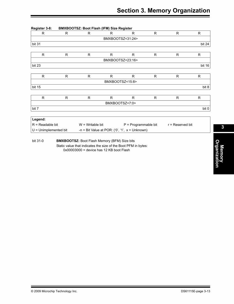
3.2.5 BMXBOOTSZ RegisterThis register configures the size of the Boot Program Flash Memory in bytes.
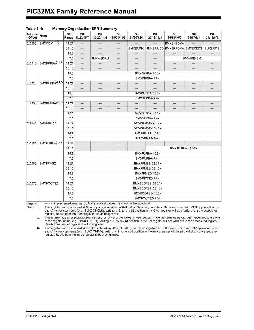
Table 3-1 provides a brief summary of all Memory Organization-related registers. Correspondingregisters appear after the summary, followed by a detailed description of each register.
Legend: — = unimplemented, read as ‘0’. Address offset values are shown in hexadecimal.Note 1: This register has an associated Clear register at an offset of 0x4 bytes. These registers have the same name with CLR appended to the
end of the register name (e.g., BMXCONCLR). Writing a ‘1’ to any bit position in the Clear register will clear valid bits in the associated register. Reads from the Clear register should be ignored.
2: This register has an associated Set register at an offset of 0x8 bytes. These registers have the same name with SET appended to the end of the register name (e.g., BMXCONSET). Writing a ‘1’ to any bit position in the Set register will set valid bits in the associated register. Reads from the Set register should be ignored.
3: This register has an associated Invert register at an offset of 0xC bytes. These registers have the same name with INV appended to the end of the register name (e.g., BMXCONINV). Writing a ‘1’ to any bit position in the Invert register will invert valid bits in the associated register. Reads from the Invert register should be ignored.
Legend:R = Readable bit W = Writable bit P = Programmable bit r = Reserved bitU = Unimplemented bit n = Bit Value at POR: (‘0’, ‘1’, x = Unknown)
bit 31-27 Reserved: Write ‘0’; ignore readbit 26 BMXCHEDMA: BMX PFM Cacheability for DMA Accesses bit
1 = Enable program Flash memory (data) cacheability for DMA accesses (requires cache to have data caching enabled)
0 = Disable program Flash memory (data) cacheability for DMA accesses (hits are still read from the cache, but misses do not update the cache)
bit 25 - 21 Reserved: Write ‘0’; ignore readbit 20 BMXERRIXI: Enable Bus Error from IXI bit
1 = Enable bus error exceptions for unmapped address accesses initiated from IXI shared bus0 = Disable bus error exceptions for unmapped address accesses initiated from IXI shared bus
bit 19 BMXERRICD: Enable Bus Error from ICD Debug Unit bit1 = Enable bus error exceptions for unmapped address accesses initiated from ICD0 = Disable bus error exceptions for unmapped address accesses initiated from ICD
bit 18 BMXERRDMA: Bus Error from DMA bit1 = Enable bus error exceptions for unmapped address accesses initiated from DMA0 = Disable bus error exceptions for unmapped address accesses initiated from DMA
bit 17 BMXERRDS: Bus Error from CPU Data Access bit (disabled in DEBUG mode)1 = Enable bus error exceptions for unmapped address accesses initiated from CPU data access0 = Disable bus error exceptions for unmapped address accesses initiated from CPU data access
bit 16 BMXERRIS: Bus Error from CPU Instruction Access bit (disabled in DEBUG mode)1 = Enable bus error exceptions for unmapped address accesses initiated from CPU instruction access0 = Disable bus error exceptions for unmapped address accesses initiated from CPU instruction access
Note 1: This register has an associated Clear register (BMXCONCLR) at an offset of 0x4 bytes. Writing a ‘1’ to anybit position in the Clear register will clear valid bits in the associated register. Reads from the Clear registershould be ignored.
2: This register has an associated Set register (BMXCONSET) at an offset of 0x8 bytes. Writing a ‘1’ to anybit position in the Set register will set valid bits in the associated register. Reads from the Set register shouldbe ignored.
3: This register has an associated Invert register (BMXCONINV) at an offset of 0xC bytes. Writing a ‘1’ to anybit position in the Invert register will invert valid bits in the associated register. Reads from the Invert registershould be ignored.
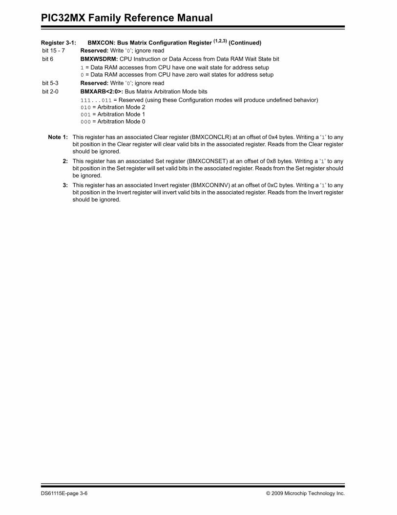
bit 15 - 7 Reserved: Write ‘0’; ignore readbit 6 BMXWSDRM: CPU Instruction or Data Access from Data RAM Wait State bit
1 = Data RAM accesses from CPU have one wait state for address setup0 = Data RAM accesses from CPU have zero wait states for address setup
bit 5-3 Reserved: Write ‘0’; ignore readbit 2-0 BMXARB<2:0>: Bus Matrix Arbitration Mode bits
111...011 = Reserved (using these Configuration modes will produce undefined behavior)010 = Arbitration Mode 2001 = Arbitration Mode 1000 = Arbitration Mode 0
Register 3-1: BMXCON: Bus Matrix Configuration Register (1,2,3) (Continued)
Note 1: This register has an associated Clear register (BMXCONCLR) at an offset of 0x4 bytes. Writing a ‘1’ to anybit position in the Clear register will clear valid bits in the associated register. Reads from the Clear registershould be ignored.
2: This register has an associated Set register (BMXCONSET) at an offset of 0x8 bytes. Writing a ‘1’ to anybit position in the Set register will set valid bits in the associated register. Reads from the Set register shouldbe ignored.
3: This register has an associated Invert register (BMXCONINV) at an offset of 0xC bytes. Writing a ‘1’ to anybit position in the Invert register will invert valid bits in the associated register. Reads from the Invert registershould be ignored.
Legend:R = Readable bit W = Writable bit P = Programmable bit r = Reserved bitU = Unimplemented bit -n = Bit Value at POR: (‘0’, ‘1’, x = Unknown)
bit 31-16 Reserved: Write ‘0’; ignore readbit 15-11 BMXDKPBA<15:11>: DRM Kernel Program Base Address bits
When non-zero, this value selects the relative base address for kernel program space in RAMbit 10-0 BMXDKPBA<10:0>: Read-Only bits
Value is always ‘0’, which forces 2 KB increments
Note 1: This register has an associated Clear register (BMXDKPBACLR) at an offset of 0x4 bytes. Writing a ‘1’ toany bit position in the Clear register will clear valid bits in the associated register. Reads from the Clearregister should be ignored.
2: This register has an associated Set register (BMXDKPBASET) at an offset of 0x8 bytes. Writing a ‘1’ toany bit position in the Set register will set valid bits in the associated register. Reads from the Set registershould be ignored.
3: This register has an associated Invert register (BMXDKPBAINV) at an offset of 0xC bytes. Writing a ‘1’ toany bit position in the Invert register will invert valid bits in the associated register. Reads from the Invertregister should be ignored.
Legend:R = Readable bit W = Writable bit P = Programmable bit r = Reserved bitU = Unimplemented bit -n = Bit Value at POR: (‘0’, ‘1’, x = Unknown)
bit 31-16 Reserved: Write ‘0’; ignore readbit 15-11 BMXDUDBA<15:11>: DRM User Data Base Address bits
When non-zero, the value selects the relative base address for User mode data space in RAM
Note: If non-zero, the value must be greater than BMXDKPBA.bit 10-0 BMXDUDBA<10:0>: Read-Only bits
Value is always ‘0’, which forces 2 KB increments
Note 1: This register has an associated Clear register (BMXDUDBACLR) at an offset of 0x4 bytes. Writing a ‘1’ toany bit position in the Clear register will clear valid bits in the associated register. Reads from the Clearregister should be ignored.
2: This register has an associated Set register (BMXDUDBASET) at an offset of 0x8 bytes. Writing a ‘1’ toany bit position in the Set register will set valid bits in the associated register. Reads from the Set registershould be ignored.
3: This register has an associated Invert register (BMXDUDBAINV) at an offset of 0xC bytes. Writing a ‘1’ toany bit position in the Invert register will invert valid bits in the associated register. Reads from the Invertregister should be ignored.
Legend:R = Readable bit W = Writable bit P = Programmable bit r = Reserved bitU = Unimplemented bit -n = Bit Value at POR: (‘0’, ‘1’, x = Unknown)
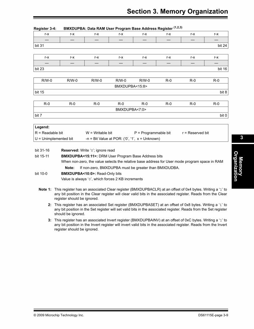
bit 31-16 Reserved: Write ‘0’; ignore readbit 15-11 BMXDUPBA<15:11>: DRM User Program Base Address bits
When non-zero, the value selects the relative base address for User mode program space in RAM
Note: If non-zero, BMXDUPBA must be greater than BMXDUDBA.bit 10-0 BMXDUPBA<10:0>: Read-Only bits
Value is always ‘0’, which forces 2 KB increments
Note 1: This register has an associated Clear register (BMXDUPBACLR) at an offset of 0x4 bytes. Writing a ‘1’ toany bit position in the Clear register will clear valid bits in the associated register. Reads from the Clearregister should be ignored.
2: This register has an associated Set register (BMXDUPBASET) at an offset of 0x8 bytes. Writing a ‘1’ toany bit position in the Set register will set valid bits in the associated register. Reads from the Set registershould be ignored.
3: This register has an associated Invert register (BMXDUPBAINV) at an offset of 0xC bytes. Writing a ‘1’ toany bit position in the Invert register will invert valid bits in the associated register. Reads from the Invertregister should be ignored.
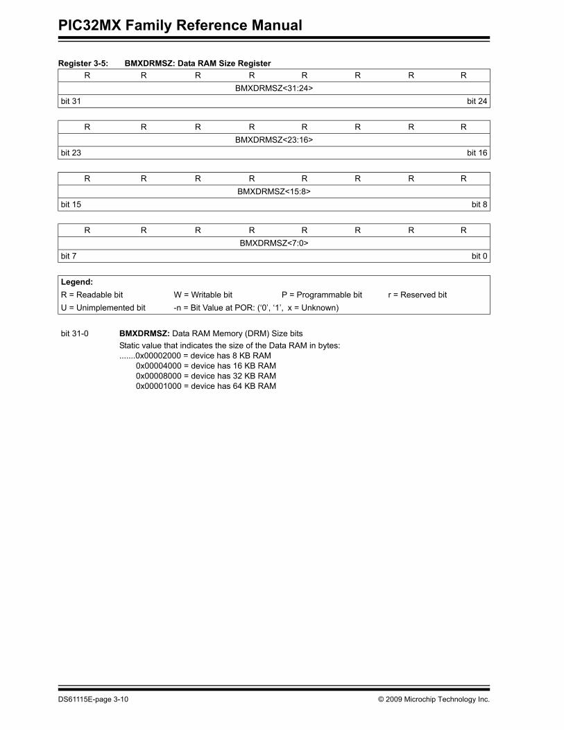
Register 3-5: BMXDRMSZ: Data RAM Size RegisterR R R R R R R R
BMXDRMSZ<31:24>bit 31 bit 24
R R R R R R R RBMXDRMSZ<23:16>
bit 23 bit 16
R R R R R R R RBMXDRMSZ<15:8>
bit 15 bit 8
R R R R R R R RBMXDRMSZ<7:0>
bit 7 bit 0
Legend:R = Readable bit W = Writable bit P = Programmable bit r = Reserved bitU = Unimplemented bit -n = Bit Value at POR: (‘0’, ‘1’, x = Unknown)
bit 31-0 BMXDRMSZ: Data RAM Memory (DRM) Size bitsStatic value that indicates the size of the Data RAM in bytes:.......0x00002000 = device has 8 KB RAM
0x00004000 = device has 16 KB RAM0x00008000 = device has 32 KB RAM0x00001000 = device has 64 KB RAM
Legend:R = Readable bit W = Writable bit P = Programmable bit r = Reserved bitU = Unimplemented bit -n = Bit Value at POR: (‘0’, ‘1’, x = Unknown)
bit 31-20 Reserved: Write ‘0’; ignore readbit 19-11 BMXPUPBA<19:11>: Program Flash (PFM) User Program Base Address bitsbit 10-0 BMXPUPBA<10:0>: Read-Only bits
Value is always ‘0’, which forces 2 KB increments
Note 1: This register has an associated Clear register (BMXPUPBACLR) at an offset of 0x4 bytes. Writing a ‘1’ toany bit position in the Clear register will clear valid bits in the associated register. Reads from the Clearregister should be ignored.
2: This register has an associated Set register (BMXPUPPBASET) at an offset of 0x8 bytes. Writing a ‘1’ toany bit position in the Set register will set valid bits in the associated register. Reads from the Set registershould be ignored.
3: This register has an associated Invert register (BMXPUPBAINV) at an offset of 0xC bytes. Writing a ‘1’ toany bit position in the Invert register will invert valid bits in the associated register. Reads from the Invertregister should be ignored.
3.3 PIC32MX MEMORY LAYOUTThe PIC32MX microcontrollers implement two address spaces: virtual and physical. All hardwareresources, such as program memory, data memory and peripherals, are located at their respec-tive physical addresses. Virtual addresses are exclusively used by the CPU to fetch and executeinstructions. Physical addresses are used by peripherals, such as DMA and Flash controllers,that access memory independently of the CPU.
Figure 3-1: Virtual to Physical Fixed Memory Mapping
The entire 4 GB virtual address space is divided into two primary regions: user and kernel space.The lower 2 GB of space from the User mode segment is called USEG/KUSEG. A User modeapplication must reside and execute in the USEG segment. The USEG segment is also availableto all Kernel mode applications, which is why it is also named KUSEG – to indicate that it is avail-able to both User and Kernel modes. When operating in User mode, the bus matrix must be con-figured to make part of the Flash and data memory available in the USEG/KUSEG segment. SeeSection 3.4 “PIC32MX Address Map” for more details.
Figure 3-2: User/Kernel Address Segments
The upper 2 GB of virtual address space forms the kernel only space. The kernel space is dividedinto four segments of 512 MB each: KSEG0, KSEG1, KSEG2 and KSEG3. Only Kernel modeapplications can access kernel space memory. The kernel space includes all peripheral registers.Consequently, only Kernel mode applications can monitor and manipulate peripherals. OnlyKSEG0 and KSEG1 segments point to real memory resources. Segment KSEG2 is available tothe EJTAG probe debugger, as explained in the MIPS documentation (refer to the EJTAGspecification). The PIC32MX only uses KSEG0 and KSEG1 segments. The Boot Flash Memory(BFM), Program Flash Memory (PFM), Data RAM Memory (DRM) and peripheral SFRs areaccessible from either KSEG0 or KSEG1.
The Fixed Mapping Translation (FMT) unit translates the memory segments into correspondingphysical address regions. Figure 3-1 shows the fixed mapping scheme implemented by thePIC32MX core between the virtual and physical address space. A virtual memory segment mayalso be cached, provided the cache module is available on the device. Please note that theKSEG1 memory segment is not cacheable, while KSEG0 and USEG/KUSEG are cacheable.
The mapping of the memory segments depend on the CPU error level (set by the ERL bit in theCPU Status register). Error Level is set (ERL = 1) by the CPU on a Reset, Soft Reset or NMI. Inthis mode, the processor runs in Kernel mode and USEG/KUSEG are treated as unmapped anduncached regions, and the mapping in Figure 3-1 does not apply. This mode is provided forcompatibility with other MIPS processor cores that use a TLB-based MMU. The C start-up codeclears the ERL bit to zero, so that when application software starts up, it sees the proper virtualto physical memory mapping as depicted in Figure 3-1.
Segments KSEG0 and KSEG1 are always translated to physical address 0x0. This translationarrangement allows the CPU to access identical physical addresses from two separate virtualaddresses: one from KSEG0 and the other from KSEG1. As a result, the application can chooseto execute the same piece of code as either cached or uncached. See Section 4. “PrefetchCache Module” (DS61119) for more details. The on-chip peripherals are visible through KSEG1segment only (uncached access).
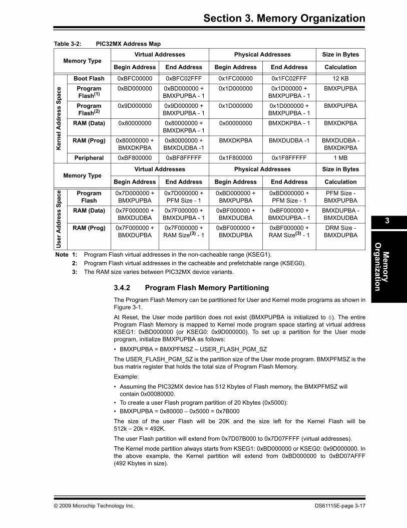
3.4 PIC32MX ADDRESS MAPThe Program Flash Memory is divided into kernel and user partitions. The kernel program Flash space starts at physical address 0x1D000000, whereas the user program Flash space starts at physical address 0xBD000000 + BMXPUDBA register value. Similarly, the internal RAM is also divided into kernel and user partitions. The kernel RAM space starts at physical address 0x00000000, whereas the user RAM space starts at physical address 0xBF000000 + BMXDUDBA register value. By default, the full Flash memory and RAM are mapped to Kernel mode application only.
Please note that the BMXxxxBA register settings must match the memory model of the targetsoftware application. If the linked code does not match the register values, the program may notrun and may generate bus error exceptions on start-up.
3.4.1 Virtual to Physical Address Calculation (and Vice-Versa)To translate the kernel address (KSEG0 or KSEG1) to a physical address, perform a “BitwiseAND” operation of the virtual address with 0x1FFFFFFF:
• Physical Address = Virtual Address and 0x1FFFFFFF
For physical address to KSEG0 virtual address translation, perform a “Bitwise OR” operation ofthe physical address with 0x80000000:
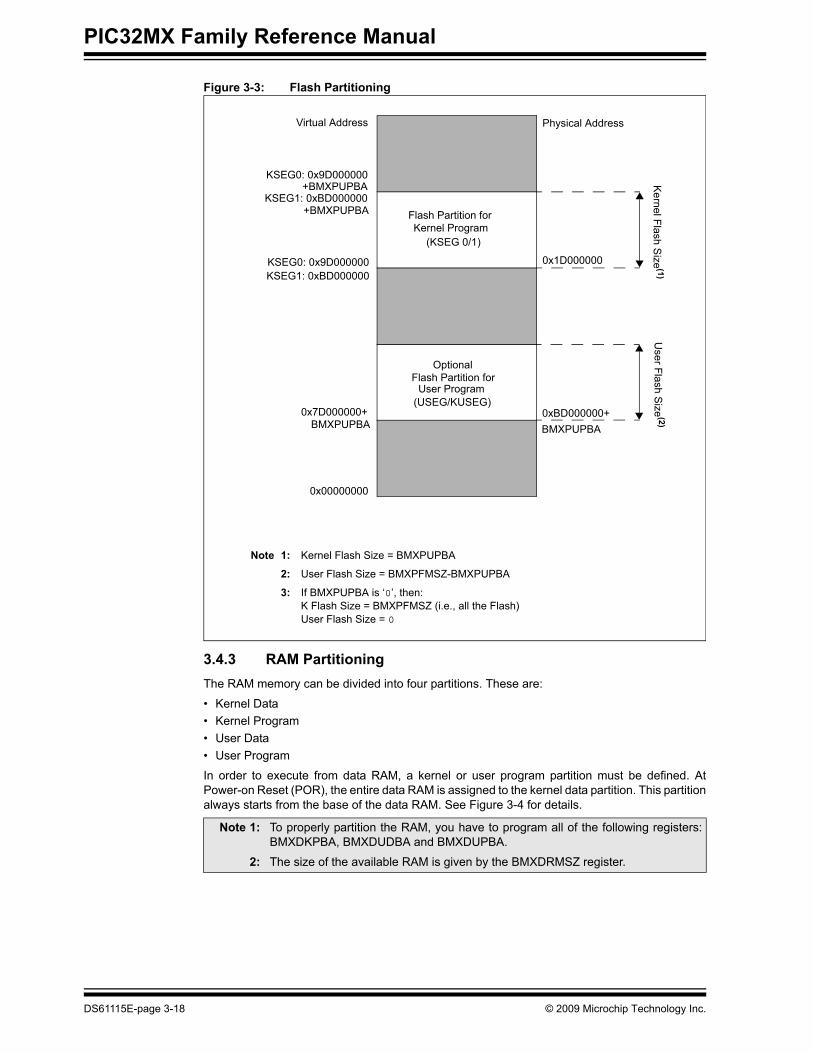
3.4.2 Program Flash Memory PartitioningThe Program Flash Memory can be partitioned for User and Kernel mode programs as shown inFigure 3-1.
At Reset, the User mode partition does not exist (BMXPUPBA is initialized to 0). The entireProgram Flash Memory is mapped to Kernel mode program space starting at virtual addressKSEG1: 0xBD000000 (or KSEG0: 0x9D000000). To set up a partition for the User modeprogram, initialize BMXPUPBA as follows:
• BMXPUPBA = BMXPFMSZ – USER_FLASH_PGM_SZ
The USER_FLASH_PGM_SZ is the partition size of the User mode program. BMXPFMSZ is thebus matrix register that holds the total size of Program Flash Memory.
Example:
• Assuming the PIC32MX device has 512 Kbytes of Flash memory, the BMXPFMSZ will contain 0x00080000.
• To create a user Flash program partition of 20 Kbytes (0x5000):• BMXPUPBA = 0x80000 – 0x5000 = 0x7B000
The size of the user Flash will be 20K and the size left for the Kernel Flash will be512k – 20k = 492K.
The user Flash partition will extend from 0x7D07B000 to 0x7D07FFFF (virtual addresses).
The Kernel mode partition always starts from KSEG1: 0xBD000000 or KSEG0: 0x9D000000. Inthe above example, the Kernel partition will extend from 0xBD000000 to 0xBD07AFFF(492 Kbytes in size).
Memory TypeVirtual Addresses Physical Addresses Size in Bytes
Begin Address End Address Begin Address End Address CalculationK
Memory TypeVirtual Addresses Physical Addresses Size in Bytes
Begin Address End Address Begin Address End Address Calculation
Use
r Add
ress
Spa
ce Program Flash
0x7D000000 + BMXPUPBA
0x7D000000 + PFM Size - 1
0xBD000000 + BMXPUPBA
0xBD000000 + PFM Size - 1
PFM Size -BMXPUPBA
RAM (Data) 0x7F000000 + BMXDUDBA
0x7F000000 + BMXDUPBA - 1
0xBF000000 + BMXDUDBA
0xBF000000 + BMXDUPBA - 1
BMXDUPBA - BMXDUDBA
RAM (Prog) 0x7F000000 + BMXDUPBA
0x7F000000 + RAM Size(3) - 1
0xBF000000 + BMXDUPBA
0xBF000000 + RAM Size(3) - 1
DRM Size - BMXDUPBA
Note 1: Program Flash virtual addresses in the non-cacheable range (KSEG1).2: Program Flash virtual addresses in the cacheable and prefetchable range (KSEG0).3: The RAM size varies between PIC32MX device variants.
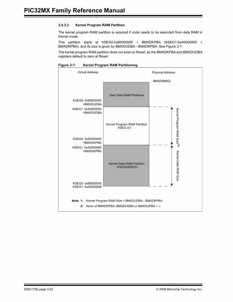
3.4.3 RAM PartitioningThe RAM memory can be divided into four partitions. These are:
• Kernel Data• Kernel Program• User Data• User Program
In order to execute from data RAM, a kernel or user program partition must be defined. AtPower-on Reset (POR), the entire data RAM is assigned to the kernel data partition. This partitionalways starts from the base of the data RAM. See Figure 3-4 for details.
Note 1: To properly partition the RAM, you have to program all of the following registers:BMXDKPBA, BMXDUDBA and BMXDUPBA.
2: The size of the available RAM is given by the BMXDRMSZ register.
Note 1: Kernel Flash Size = BMXPUPBA
2: User Flash Size = BMXPFMSZ-BMXPUPBA
3: If BMXPUPBA is ‘0’, then:K Flash Size = BMXPFMSZ (i.e., all the Flash)User Flash Size = 0
5: If BMXDKPBA, BMXDUDBA or BMXDUPBA is ‘0’, then:Kernel Data RAM Size = BMXDRMSZ (i.e., all RAM)Kernel Program RAM Size = 0User Data RAM Size = 0User Program RAM Size = 0
The kernel data RAM partition is located at virtual address KSEG0:0x80000000,KSEG1:0xA0000000. It is always active and cannot be disabled.
Please note that if any of the BMXDKPBA, BMXDUDBA or BMXDUPBA register is ‘0’, then thewhole RAM is assigned to kernel data RAM (i.e., the size of the kernel data RAM partition is givenby the BMXDRMSZ register value; see Figure 3-5). Otherwise, the size of the kernel data RAMpartition is given by the value of the BMXDKPBA register (see Figure 3-6).
The kernel data RAM partition exists on Reset and takes up all the available RAM, as theBMXDKPBA, BMXDUDBA and BMXDUPBA registers default to zero at any Reset.
Figure 3-5: RAM Partitioning When BMXDKPBA, BMXDUDBA or BMXDUPBA = 0
For User mode applications, a User mode data partition in RAM is required. This partition startsat address 0x7F000000 + BMXDUDBA, and its size is given by BMXDUPBA - BMXDUDBA (seeFigure 3-8).
The user data RAM partition does not exist on Reset, as the BMXDUDBA and BMXDUPBAregisters default to zero at Reset.
Figure 3-8: User Data RAM Partitioning
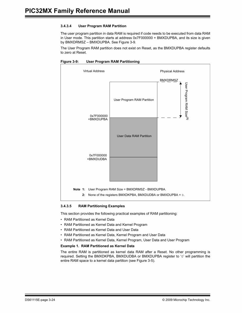
Note 1: User Data RAM Size = BMXDUPBA - BMXDUDBA.
2: None of the registers BMXDKPBA, BMXDUDBA or BMXDUPBA = 0.
The user program partition in data RAM is required if code needs to be executed from data RAMin User mode. This partition starts at address 0x7F000000 + BMXDUPBA, and its size is givenby BMXDRMSZ – BMXDUPBA. See Figure 3-9.
The User Program RAM partition does not exist on Reset, as the BMXDUPBA register defaultsto zero at Reset.
Figure 3-9: User Program RAM Partitioning
3.4.3.5 RAM Partitioning Examples
This section provides the following practical examples of RAM partitioning:
• RAM Partitioned as Kernel Data• RAM Partitioned as Kernel Data and Kernel Program• RAM Partitioned as Kernel Data and User Data• RAM Partitioned as Kernel Data, Kernel Program and User Data• RAM Partitioned as Kernel Data, Kernel Program, User Data and User Program
Example 1. RAM Partitioned as Kernel DataThe entire RAM is partitioned as kernel data RAM after a Reset. No other programming isrequired. Setting the BMXDKPBA, BMXDUDBA or BMXDUPBA register to ‘0’ will partition theentire RAM space to a kernel data partition (see Figure 3-5).
Note 1: User Program RAM Size = BMXDRMSZ - BMXDUPBA.
2: None of the registers BMXDKPBA, BMXDUDBA or BMXDUPBA = 0.
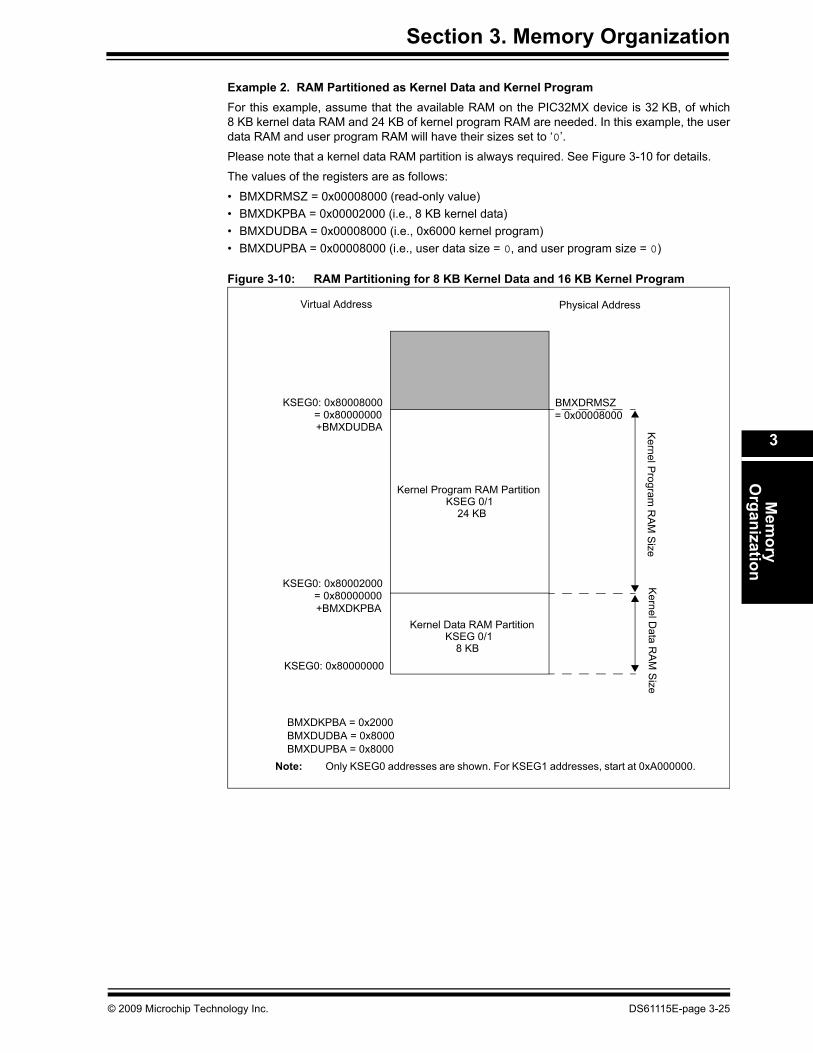
Example 2. RAM Partitioned as Kernel Data and Kernel ProgramFor this example, assume that the available RAM on the PIC32MX device is 32 KB, of which8 KB kernel data RAM and 24 KB of kernel program RAM are needed. In this example, the userdata RAM and user program RAM will have their sizes set to ‘0’.
Please note that a kernel data RAM partition is always required. See Figure 3-10 for details.
The values of the registers are as follows:
• BMXDRMSZ = 0x00008000 (read-only value)• BMXDKPBA = 0x00002000 (i.e., 8 KB kernel data)• BMXDUDBA = 0x00008000 (i.e., 0x6000 kernel program)• BMXDUPBA = 0x00008000 (i.e., user data size = 0, and user program size = 0)
Figure 3-10: RAM Partitioning for 8 KB Kernel Data and 16 KB Kernel Program
Example 3. RAM Partitioned as Kernel Data and User DataFor this example, assume that the available RAM on the PIC32MX device is 32 KB, of which16 KB of kernel data RAM and 16 KB of user data RAM are needed. In this example, the kernelprogram RAM and user program RAM will have their sizes set to ‘0’. See Figure 3-11 for details.
The values of the registers are as follows:
• BMXDRMSZ = 0x00008000 (read-only value)• BMXDKPBA = 0x00004000 (i.e., 16 KB kernel data)• BMXDUDBA = 0x00004000 (i.e., 0 kernel program)• BMXDUPBA = 0x00008000 (i.e., user data size = 16 KB, and user program size = 0)
Figure 3-11: RAM Partitioning for 16 KB Kernel Data and 16 KB User Data
Example 4. RAM Partitioned as Kernel Data, Kernel Program and User DataFor this example, assume that the available RAM on the PIC32MX device is 32 KB, and 4 KB ofkernel data RAM, 6 KB of kernel program and 22 KB of user data RAM are needed. In thisexample, the user program RAM will have its size set to ‘0’. See Figure 3-12 for details.
The values of the registers are as follows:
• BMXDRMSZ = 0x00008000 (read-only value)• BMXDKPBA = 0x00001000 (i.e., 4 KB kernel data)• BMXDUDBA = 0x00002800 (i.e., 6 KB kernel program)• BMXDUPBA = 0x00008000 (i.e., user data size = 22 KB, and user program size = 0)
Figure 3-12: RAM Partitioning for 4 KB K-Data, 6 KB K-Program and 22 KB U-Data
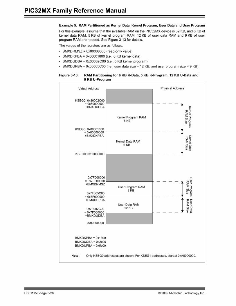
Example 5. RAM Partitioned as Kernel Data, Kernel Program, User Data and User ProgramFor this example, assume that the available RAM on the PIC32MX device is 32 KB, and 6 KB ofkernel data RAM, 5 KB of kernel program RAM, 12 KB of user data RAM and 9 KB of userprogram RAM are needed. See Figure 3-13 for details.
The values of the registers are as follows:
• BMXDRMSZ = 0x00008000 (read-only value)• BMXDKPBA = 0x00001800 (i.e., 6 KB kernel data)• BMXDUDBA = 0x00002C00 (i.e., 5 KB kernel program)• BMXDUPBA = 0x00005C00 (i.e., user data size = 12 KB, and user program size = 9 KB)
Figure 3-13: RAM Partitioning for 6 KB K-Data, 5 KB K-Program, 12 KB U-Data and 9 KB U-Program
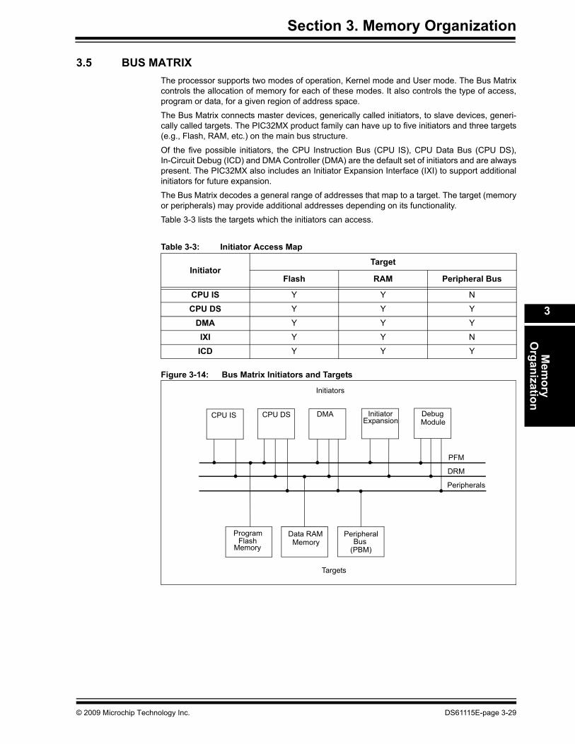
3.5 BUS MATRIXThe processor supports two modes of operation, Kernel mode and User mode. The Bus Matrixcontrols the allocation of memory for each of these modes. It also controls the type of access,program or data, for a given region of address space.
The Bus Matrix connects master devices, generically called initiators, to slave devices, generi-cally called targets. The PIC32MX product family can have up to five initiators and three targets(e.g., Flash, RAM, etc.) on the main bus structure.
Of the five possible initiators, the CPU Instruction Bus (CPU IS), CPU Data Bus (CPU DS),In-Circuit Debug (ICD) and DMA Controller (DMA) are the default set of initiators and are alwayspresent. The PIC32MX also includes an Initiator Expansion Interface (IXI) to support additionalinitiators for future expansion.
The Bus Matrix decodes a general range of addresses that map to a target. The target (memoryor peripherals) may provide additional addresses depending on its functionality.
Table 3-3 lists the targets which the initiators can access.
3.5.1 Initiator Arbitration ModesSince there can be more than one initiator attempting to access the same target, an arbitrationscheme must be used to control access to the target. The arbitration modes assign priority levelsto all the initiators. The initiator with the higher priority level will always win target access over alower priority initiator.
3.5.1.1 Arbitration Mode 0
The fixed priority scheme in Arbitration Mode 0 is shown in Figure 3-15. The CPU data andinstruction access are given higher priority than DMA access. This mode can starve the DMA, sochose this mode when DMA is not being used.
As shown in Figure 3-15, each initiator is assigned a fixed priority level. Programming the registerfield BMXARB (BMXCON<2:0>) to ‘0’ selects Mode 0 operation.
Figure 3-15: Priority Assignment in Arbitration Mode 0
Arbitration Mode 1 is a fixed priority scheme like Mode 0; however, the CPU IS is always thelowest priority. Figure 3-16 shows the priority scheme in Mode 1. Mode 1 arbitration is the defaultmode.
Programming the register field BMXARB (BMXCON<2:0>) to ‘1’ selects Mode 1 operation.
Figure 3-16: Priority Assignment in Arbitration Mode 1
Mode 2 arbitration supports rotating priority assignments to all initiators. Instead of a fixed prior-ity assignment, each initiator is assigned the highest priority in a rotating fashion. In this mode,the rotating priority is applied with the following exceptions:
1. CPU data is always selected over CPU instruction.2. ICD is always the highest priority.3. When the CPU is processing an exception (EXL = 1) or an error (ERL = 1), the arbiter
temporarily reverts to Mode 0.
Figure 3-17: Priority Assignments in Arbitration Mode 2
Note that priority sequence 2 is not selected in the rotating priority scheme if there is a pendingCPU data access. In this case, once the data access is complete, sequence 2 is selected.
Programming the register field BMXARB (BMXCON<2:0>) to ‘2’ selects Mode 2 operation.
3.5.2 Bus Error ExceptionsThe Bus Matrix generates a bus error exception on:
• Any attempt to access unimplemented memory• Any attempt to access an illegal target• Any attempt to write to program Flash memory
Bus Error Exceptions may be temporarily disabled by clearing the BMXERRxxx bits in theBMXCON register, which is not recommended.
The Bus Matrix disables bus error exceptions for accesses from CPU IS and CPU DS while inDEBUG mode.
3.5.3 Break Exact Breakpoint SupportThe PIC32MX supports break exact breakpoints by inserting one Wait state to data RAM access.This method allows the CPU to stop execution just before the breakpoint address instruction.This is useful in case of breakpointed store instructions. When the Wait state is not used, thebreak will still occur at the store instruction, however, the DRM location is updated with the storevalue. If the Wait state is enabled the DRM is not updated with the store value.
3.6 I/O PIN CONTROLThere are no pins associated with this module.
3.7 OPERATION IN POWER-SAVING AND DEBUG MODES
3.7.1 Memory Operation on Power-up or Brown-out Reset (BOR):• The contents of data RAM are undefined• The BMXxxxBA registers are reset to ‘0’• CPU is switched to Kernel mode
3.7.2 Memory Operation on Reset:• The data RAM contents are retained. If the device is code-protected, the RAM contents are
cleared• The BMX base address registers (BMXxxxBA) are set to ‘0’• CPU is switched to Kernel mode
3.7.3 Memory Operation on Wake-up from Device Sleep or Idle Mode:• The RAM contents are retained• The BMX base address register (BMXxxxBA) contents are not changed• CPU mode is unchanged
BMXDKPBA = 12*1024; // Kernel Data Partition of 12K.// Start offset of Kernel Program Partition
BMXDUDBA = BMXDKPBA + (6*1024); // Kernel Program Partition of 6K// Start offset of User Data Partition
BMXDUPBA = BMXDUDBA + (8*1024); // User Data Partition of 8K// Start offset of User Program Partition.// This partition will go up to the size of// RAM (32K). So the partition size will be// 6K (32K - 8K - 6K - 12K)
Question 1: At Reset, in which mode is the CPU running?Answer: The CPU starts in Kernel mode. The entire RAM is mapped to kernel data
segments in KSEG0 and KSEG1. Flash memory is mapped to kernel programsegments in KSEG0 and KSEG1. Also ERL = 1, which should be reset to zero(normally in the C start-up code).
Question 2: Do I need to initialize the BMX registers?Answer: Generally, no. You can leave the BMX registers at their default values, which
allows maximum RAM and Flash memories for Kernel mode applications. If youwant to run code from RAM or set up User mode partitions, you will need toconfigure the BMX registers.
Question 3: What is the CPU Reset vector address?Answer: The CPU Reset address is 0xBFC00000.
Question 4: What is a Bus-Error Exception?Answer: Bus-error exceptions are generated when the CPU tries to access
unimplemented addresses. Also, when the CPU tries to execute a program fromRAM without defining a RAM program partition, a bus-error exception isgenerated.
3.10 RELATED APPLICATION NOTESThis section lists application notes that are related to this section of the manual. These applica-tion notes may not be written specifically for the PIC32MX device family, but the concepts arepertinent and could be used with modification and possible limitations. The current applicationnotes related to the Memory Organization of the PIC32MX family include the following:
Title Application Note #No related application notes at this time. N/A
Note: Please visit the Microchip web site (www.microchip.com) for additional applicationnotes and code examples for the PIC32MX family of devices.
Revision A (August 2007)This is the initial released version of this document.
Revision B (October 2007)Updated document to remove Confidential status.
Revision C (April 2008)Revised status to Preliminary; Revised U-0 to r-x.
Revision D (June 2008)Change Reserved bits from “Maintain as” to “Write”.
Revision E (July 2009)This revision includes the following updates:
• Minor updates to the text and formatting have been incorporated throughout the document• Added Notes 1, 2 and 3, which describe the Clear, Set and Invert registers to the following:
- Table 3-1: Memory Organization SFR Summary- Register 3-1: BMXCON: Bus Matrix Configuration Register- Register 3-2: BMXDKPBA: Data RAM Kernel Program Base Address Register- Register 3-3: BMXDUDBA: Data RAM User Data Base Address Register- Register 3-4: BMXDUPBA: Data RAM User Program Base Address Register- Register 3-6: BMXPUPBA: Program Flash (PFM) User Program Base Address Register
• Removed all Clear, Set and Invert register descriptions• Added additional bit value definition (0x0001000) to BMXDRMSZ: Data RAM Size Register