Page 1
LAPPEENRANTA UNIVERSITY OF TECHNOLOGY
Faculty of Technology
Double Degree Programme in Technical Physics
Anatoly Fominykh
PIEZO FORCE MICROSCOPY AND PEAKFORCE TUNA
MEASUREMENTS OF III-V SEMICONDUCTOR NANOWIRES
Examiners: Professor Erkki Lähderanta
M. Sc. Pavel Geydt
Page 2
2
ABSTRACT
Lappeenranta University of Technology
Faculty of Technology
Degree Programme in Technomathematics and Technical Physics
Anatoly Fominykh
PIEZO FORCE MICROSCOPY AND PEAKFORCE TUNA
MEASUREMENTS OF III-V SEMICONDUCTOR NANOWIRES
Master‟s thesis
2016
51 pages, 38 figures, 3 tables.
Keywords: Atomic Force Microscopy, Piezo Force Microscopy, PeakForce TUNA, Nanowire,
InP, GaAs, GaN, A3B5, piezo response.
GaN, InP and GaAs nanowires were investigated for piezoelectric response. Nanowires and
structures based on them can find wide applications in areas purposes such as nanogenarators,
nanodrives, Solar cells and other perspective areas.
Experemental measurements were carried out on AFM Bruker multimode 8 and data was
handled with Nanoscope software. AFM techniques permitted not only to visualize the surface
topography, but also to show distribution of piezoresponse and allowed to calculate its
properties. The calculated values are in the same range as published by other authors.
Page 3
3
ACKNOWLEDGEMENTS
I am pleased to thank Professor Erkki Lähderanta for giving me opportunity to study at
Lappeenranta University of Technology and for conducting me throw study and research. I
would like to thank my supervisor Pavel Geydt for his patience, comments, and support.
I would also like to say that I am grateful to Professor V. A. Moshnikov for all his advices and
support in last 3 years, as well to many others from department of Micro- and Nanoelectronics in
St. Petersburg State Electrotechnical University.
I am really grateful to my family and friends, especially O.L.
Lappeenranta, May 2016
Anatoly Fominykh
Page 4
4
Table of Contents
1. Introduction ............................................................................................................................................... 6
2. Nanowires ................................................................................................................................................. 8
2.1 Synthesis of nanowires ............................................................................................................................ 8
2.2 Applications of Nanowires .................................................................................................................... 12
2.3 Conclusion about nanowires ................................................................................................................. 17
3. Methodical Section .................................................................................................................................. 18
3.1. Scanning Probe Microscopy: basic principles ...................................................................................... 18
3.2. Atomic Force Microscopy (AFM) ....................................................................................................... 19
3.3. Piezoelectric Force Microscopy ........................................................................................................... 26
3.4. PeakForce TUNA ................................................................................................................................. 27
3.5. Kelvin mode ......................................................................................................................................... 29
4. Samples ............................................................................................................................................... 31
5. Experiments and results .......................................................................................................................... 36
5.1. Measurement sequence ........................................................................................................................ 36
5.2 Experiments ........................................................................................................................................... 37
Conclusions ................................................................................................................................................. 47
Summary ..................................................................................................................................................... 48
References ................................................................................................................................................... 50
Page 5
5
List of Abbreviations
AFM Atomic Force Microscopy; Atomic Force Microscope (device)
ALD Atomic Layer Deposition
CPD Contact Potential Difference
DFL Deflection signal difference between top and bottom halves of the photodiode
EFM Electric Force Microscopy
FET Field Effect Transistor
KPFM Kelvin Probe Force Microscopy
LF Difference signal between left and right halves of the photodiode
MAG Magnitude of AFM probe oscillations in Semicontact mode
MBE Molecular Beam Epitaxy
MOSFET Metal-Oxide-Semiconductor Field Effect Transistor
NWs nanowires
PLD Pulsed Laser Deposition
PFM piezo force microscopy
QDs Quantum dots
SP Surface Potential
SPM Scanning Probe Microscopy
STM Scanning Tunneling Microscopy
UHV Ultra High Vacuum
Page 6
6
1. Introduction
Nowadays, nanotechnology is one of the most rapidly developing and promising area of modern
science. Nanotechnology can be described as a set of technological methods used for the study,
design and production of materials, devices and systems, including the targeted control and
management structure, chemical composition and interaction of the constituent elements of
individual nanoscale. Alternatively, nanotechnology can be defined as „knowledge and
management processes, usually on a scale of nanometers, but not precluding the scale of less
than 100 nm in one or more dimensions, when put into operation the size effect (phenomenon)
leads to the possibility of new applications.
Exist many reasons for such interest to nanoscale technologies. At the first, various materials,
that are well-known, have unexpected properties in the scale of nanometers, This is connected
with size effect. At the second, modern consumers are requiring smaller and smaller devises with
good properties. As an example can be taken progress of laptops in last 30 years. At the third,
classic planar technologies based on silicon are well-studied, but have many limitations. Finally,
already now exist devises based on nanotechnologies products wich can replace huge old-school
systems, such as „lab-on-a-chip‟ used for express analyses. They work faster in comparison with
old devises and more comfortable for personal use.
One interesting topic among nanotechnologies is study of nanowire. Exist also nanorods and
nanopillars, but difference between them and nanowires is important mainly in terminology due
to different length-to-wide ratios.
Nanowire is nanostructure, with the diameter of the order of a nanometer (10−9
meters).
Another definition of nanowire is a structure with the ratio of the length to width being
greater than 1000.
With the same diameter as nanowire, nanorod‟s aspect ratio is from 3 to 5.
Nanopillar‟s aspect ratio is in between nanowire and nanorod.
It is possible to group nanorods, nanowires, nanopillars all together and call them nanowires,
because this is new area of science and actually terminology is not yet well defined. It might be
comfortable to use special terms only to underline that some special properties exist in those
Page 7
7
aspect ratio. Other names for such structures exist, like nanowhiskers, nano-antenna. This is
actually also a name for different devises based on nanowires.
Typical aspect ratios (length-to-width ratio) for nanowires are high, but not always more than
1000. For many purposes lower ratios are required. For example, in our measurements length of
nanowire more than 1µm might cause some additional problems and mistakes. Also various
purposes might require diameter of structures more than 100 nm, but it still is possible to call
them nanostructure as their fabrication technologies are same and properties are different from
bulk materials. It is important that nanowires have such scale that quantum mechanic effects start
to influence the properties of nanowire or/and crystal structure is different comparing to bulk
material.
Some nanowires may have piezoelectric properties. Piezoelectricity can be defined as the electric
charge that appears in certain solid materials in response to applied mechanical stress. Usually in
the same materials also exist reverse piezoelectric properties – with electric field applied to the
sample it‟s geometric sizes changes. Based on those properties of nanowires they can find many
purposes having no competitors, such as high quality and cheap nanodrives and gyroscopes of
extremely small size.
For investigation of local properties of nanoscale materials it is preferably to use methods, which
can provide resolution up to nanometers.
The motivation of this work was to investigate the piezoelectric properties of nanowires
produced from different materials.
Page 8
8
2. Nanowires
Nanowires (nanorods, nanowhiskers and etc.) have variety of unique properties and differences
from bulk materials. Research and explanation nanowires is very innovative, so it is not always
enough data for sure conclusions.
In this chapter some of them are explained, as well as synthesis, properties and applications are
described.
2.1 Synthesis of nanowires
Different technologies allow growing of nanowires with various speed and also with different
sizes, crystal structure, impurity type and level, coating etc. Second important fact is that
nanowires are organized on the substrate and geometric properties of same series depends from
growth technology. Exist technologies when nanowires grow vertical, even with some angle to
substrate. This depends from angle between substrates surface and source of reagents. This kind
of structure are also possible to organize in lattice with constant distant between nanowires.
Chaotically ordered nanowires are less used due to low repeatability and they are mostly
produced in liquid environment.
Exist two main approaches to sintering nanowires: bottom-up and top-down. One example of
top-down is reducing size of bigger wire to reduce size, and bottom-up is growing of nanowire
by atoms or molecules or layers. On list below are some techniques to produce nanowires.
Chemical Vapor Deposition. CVD is chemical process widely used to grow solid materials in
reaction chamber. Growth is realized by exposure of substrate for different volatile precursors
and their reaction on surface of the sample. Precursors are moving to substrate by inert gas flow,
which also moves reaction products away from growth area.
Atomic Layer Deposition. ALD is a thermally activated gas phase process to synthesize thin
solid films by exposing an object to series of at least two gaseous precursors, each one is self-
limiting chemisorption surface reactions. High vacuum camera is required for such process for
better quality and less crystal defects. ALD process scheme is demonstrated on Fig. 1 [1].
Page 9
9
Pic. 1. ALD process stages.[1]
Method is used for thin-films, but it allows to produce nanowires, usually with use of specially
prepared substrate [2]. ALD technique can be defined as sub-class of CVD, but extremely
precise.
Vapor–liquid–solid method. VLS is one of the most important methods for crystal growth. Fig. 2
- 4 demonstrates the scheme of VLS mechanism. Technology of VLS uses catalytic drop of
liquid (catalysts), which provide fast and orientated growth. Growth occurs on solid state surface
by adsorbing vapor under the liquid phase. Diameter of droplets desine the diameter of nanowire.
Samples grown in such way can be well-controlled. It is possible to organize distance between
nanowires precisely by placing catalytic drops in required pattern. VLS also is a sub-class of
CVD [3, 4].
Fig. 2. Growth of nanowires by VLS method [4]
Page 10
10
Fig. 3. Schematic of the nanowire growth dynamics. (A) Different phases of the semiconductor material
(e.g., Si) during the nanowire growth. (B) Nucleation at the three phase boundary. (C) Ledge propagation
after nucleation. (D) Complete formation of one new layer. The process is then repeated.
Fig. 4. Possible deposition pathways in a VLS system. Depending on the growth parameters, VLS growth
via catalyst alloy, radial overcoating on the existing nanowire sidewalls and thin film deposition on
substrate may occur.
Suspension. Describes top-down methods. To increase the quality a high vacuum (HV) chamber
is required. Suspension is less widely used comparing to other techniques, but it allows
producing nanowires from bulk materials or wires. Such possibility can be useful when other
methods are too complicated, usually if composition is complex. Methods to allow decreasing od
size and shaping of the sample:
chemical etching;
mechanical treatment;
ion bombardment, most often with high ion energies;
combination of different methods.
Page 11
11
Planar technology. By classical planar technology with use of photolitigraphy and etching it is
possible to create special grooves and/or channels. They are further fulfilled with required
material forming vertical and/or horizontal nanowires [6,7].
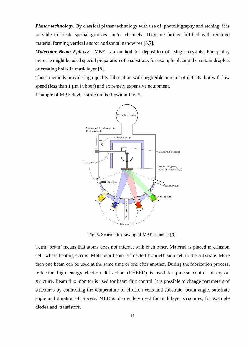
Molecular Beam Epitaxy. MBE is a method for deposition of single crystals. For quality
increase might be used special preparation of a substrate, for example placing the certain droplets
or creating holes in mask layer [8].
Those methods provide high quality fabrication with negligible amount of defects, but with low
speed (less than 1 µm in hour) and extremely expensive equipment.
Example of MBE device structure is shown in Fig. 5.
Fig. 5. Schematic drawing of MBE chamber [9].
Term „beam‟ means that atoms does not interact with each other. Material is placed in effusion
cell, where heating occurs. Molecular beam is injected from effusion cell to the substrate. More
than one beam can be used at the same time or one after another. During the fabrication process,
reflection high energy electron diffraction (RHEED) is used for precise control of crystal
structure. Beam flux monitor is used for beam flux control. It is possible to change parameters of
structures by controlling the temperature of effusion cells and substrate, beam angle, substrate
angle and duration of process. MBE is also widely used for multilayer structures, for example
diodes and transistors.
Page 12
12
Solution-phase synthesis. Describes big amount of methods, for which common part is that
procces occurs in liquid phase. Sol-gel method is one of the solution-phase synthesis. Can be
used for substrate preparation first by creating seed layer. It is layer with particles which are as
basement of nanowire during growth. Also by solution-phase synthesis methods it is possible to
create considerable amount of nanowires, which are not ordered.
It is common to use specific combination of different techniques, that allows to reach better
results by time or/and quality. Additionally, every laboratory utilize own modification of a NWs
production methods, connected with equipment, precursors and purposes of research.
2.2 Applications of Nanowires
Due to variety of properties of nanowires, multiple synthesis methods and compositions, NWs
already predicted to be used in many different areas. In some possible areas of application, NWs
have no competitors among existing devises.
It is possible to distinguish main applications of nanowires as: passive components like
electrodes or interconnections; diodes and p-n transistors, FETs, MOSFETs; LEDs; waveguides;
energy generators based on mechanical (piezoelectric for example) or quantum (QD and QW as
an example) properties; nanosize mechanical drives; mechanical sensors and gyroscopes;
photosensors; display technologies; medicine, usually as markers; tips for SPM; part of MEMS
and NEMS.
Most common and perspective purposes will be described here below in more detail.
Tips for scanning probe microscopy. Due to geometrical dimensions it is almost perfect
application for nanowires. Exist techniques to grow nanowires with diameter around 10-30 nm
with length up to 10 µm. This type of tips might have many disadvantages, like softness and
flexibility, but those shortcomings are not always critical. Benefit of such tips is that with
diameter comparable with typical for tips radius of curvature, length is much longer, allowing to
investigate samples with large height difference. Also many other advantages. For example,
already exist experimental single-crystal diamond nanowire tips which are used for ultrasensitive
force microscopy (shown in Fig. 6) [10].
Page 13
13
Fig. 6. Diamond nanowire tip.
Transistors and diodes. Classical use of nanowires is to create diode and transistors. It is
possible to create FET transistors , as it shown in Fig. 7. In bottom side of dielectric layer is
coated a gate electrode. From an opposite side is located nanowire between source and drain
electrodes. Applying voltage to gate electrode it is possible to control conductivity of nanowire
and current between source and drain.
Fig.7. FET based on nanowire.
Due to the high aspect ratio, it is possible to create FET (or MOSFET) structures, using the
nanowire as a conductive channel of such transistor. One can precisely control nanowires
electrostatic potential, thereby, turning the transistor on and off efficiently. By changing the
composition, doping level, diameter and other NWs parameters, researchers can control
threshold voltage and other characteristics.
This is possible due to precise control when producing nanowire and combination of different
technologies. Also it is possible to create p-n or hetero junctions by creating coating or
multilayer structures. Fig. 8 demonstrates heterojunction realized by coating nanowire and by
growing multilayer structures.
Page 14
14
Fig.8. Schematic of nanowire heterostructure synthesis. (a) Preferential reactant incorporation at the
catalyst (growth end) leads to one dimensional axial growth. (b) A change in the reactant leads to either
(c) axial heterostructure growth or (d) radial heterostructure growth depending on whether the reactant is
preferentially incorporated (c) at the catalyst or (d) uniformly on the wire surface. Alternating reactants
will produce (e) axial super lattices or (f) core/ shell structures.
GaAs and GaN are used as examples. Main requirements for vertical multilayer nanowire is that
lattice constant should be similar. Only in this case it is possible to grow long nanowire. But this
requirement is common for all bottom-up grow techniques, not only for NWs growth.
It is possible to create more complex active electronics components by combining nanowires in
different ways. One important feature is that NWs allows to combine classical planar
technologies with nanotechnologies. That leads to building IC based on new principles. That is
very important at our days, due to the fact that Moore‟s law is predicting limit of classic planar
transistors located on one integrated circuit.
After p-n junctions were built with nanowires, the next step was to build logic gates. By
connecting several p-n junctions together, researchers were able to create the basis of all logic
circuits: the AND, OR, and NOT gates have all been built from semiconductor nanowires.
Optical properties. Heterojunctions are often used for different optical purposes. Nanowires also
might be used as classical heterostructures.
Nanowires can act as a photon waveguides and such application might be useful in future when
creating photon-based IC or mixed photon-electron IC.
Page 15
15
It is possible to grow nanowire in such a way, that quantum dot will be included in the structure.
Other way is to make crossing to NWs so that juncture will act like QD. Nanowires with
quantum dots represent one of the most perspective technologies for different applications in
quantum photonics. For example, its widely discussed that in near future such structure can
replace other LEDs due to high efficiency and quite cheap price. [11]
Very promising area for nanowires with QD is solar energy. Quantum dots NWs might be used
for multi-junction solar cells to harvesting main part of solar spectrum. Fig. 9 shows that solar
cells production increases, demonstrating interest to solar energy and green energies.
Fig.9. Solar cell production in different regions [12]
Conducting nanowires. Most often offered use for conducting NWs is different electrodes or
interconnectors. Conducting NWs gives possibility to connect molecular scale objects to
complicated circuits. Mixed with different polymers, conducting nanowires can form transparent
films for electrodes, e.g. for solar energy and flexible electronics [13]. Use of transparent
electrode in solar cells can dramatically improves efficiency by increasing photosensitive area.
Nanowire battery. Nanowires are also possible to be used to increase surface of electrodes,
improving battery performance. NWs could increase anodes power density by increasing the
available surface area in contact with the electrolyte. Electrode‟s degradation can be decreased
with use of NWs, so it is possible to have more recharge cycles for one battery [14].
Rectenna. A rectenna (also nano-antenna) is a rectifying antenna i.e. a device which purpose is
to convert electromagnetic energy into electric current. Circuit contains an antenna and a diode
turning EM wave into direct current electricity. Use of nanotubes allow to unite antena and diode
Page 16
16
in one nanoscale device. Use of NWs also give such advantage as controlled length, that might
be as long as certain light wavelength. This makes rectenna more efficient. Controlling the size
of nanowires used for rectenna gives opportunity to create receivers optimized for specific
wavelength. As the sun light is electromagnetic (EM) wave, it is possible to construct Solar cell
based on nanowire rectennas or to modify old types of solar cells with rectennas [15]. For
example, use of rectennas with planar cells can increase adsorption of light coming to the device.
Nanogenerator is technology that converts into electric current the mechanical/thermal energy
which is produced by small-scale physical change. Basic nanogenerators are piezoelectric,
triboelectric and pyroelectric.
A piezoelectric nanogenerator is an energy generating device, based on same principles as bulk
piezomaterials. Main difference is that nanowires can harvest much smaller mechanical
pressure, such as air pressure of wind, providing new ways for green energy technologies.
The piezoelectric nanogenerator could potentially convert following types of energy into electric
energy: mechanical-movement energy, such as human body movement or pressure; vibration
energy, from acoustic or ultrasonic waves either some random sources; and hydraulic energy,
such as the flow of fluids or blood, the contraction of blood vessels, or dynamic fluid in nature
[16]. Bio-, nano- and other technologies require low power supply, but small, nano-sized energy
sources could be done from NWs.
Depending on the location of piezoelectric nanowire, the nanogenerator can be categorized into 3
main types:
1. Vertical nanowire Integrated Nanogenerator (VING), illustrated on Fig. 10.
2. Lateral nanowire Integrated Nanogenerator (LING).
3. Nanocomposite Electrical Generators (NEG).
Additionally, exist configurations that do not fall into the categories mentioned above.
Page 17
17
Fig. 10. Schematic view of typical Vertical nanowire Integrated Nanogenerator, A is electrode for
Schottky contact, B is piezonanowire, C is electrode with ohmic contact.
A triboelectric nanogenerator is an electric current generating device. It convert external
mechanical energy into current by a conjunction of triboelectric effect and electrostatic
induction.
A pyroelectric nanogenerator is an electric current generating device converting thermal energy
into an electricity by using nano-structured pyroelectric materials.
2.3 Conclusion about nanowires
Exist variety of nanowires types. As it was shown before, many of them can find use in modern
and future science and technology. Because advantages of NWs are so obvious, efforts should be
applied for their studies. Integral properties of nanowires are promising and also single nanowire
can be used for many purposes and integral diagnostic methodic should be developed.
Considering size of nanowires and the fact that many interesting properties are connected with
mechanical impacts on nanowire, one of the most promising methods is atomic force microscopy
(AFM). Combination of AFM with other methods, such as scanning electron microscope and x-
ray crystallography, can give enough data for understanding the physics and advantages of
nanowires. Because to NWs are wide class of objects, additional methods of studies are required.
Integral properties might be investigated by such methods as, for example, impedance
spectroscopy, optical spectroscopy etc.
Page 18
18
3. Methodical Section
3.1. Scanning Probe Microscopy: basic principles
Scanning probe microscopy (SPM) is a branch of microscopy methods, in which a probe is
scanning the surface of the sample. SPM was created in early 1980‟s with invention of scanning
tunneling microscope, still used as precise instrument for surface imaging. Main types of
scanning probe microscope are: atomic force microscopy; scanning tunneling microscope; near-
field scanning optical microscope.
It is typical for modern SPM to image several interactions, for example electrical, magnetic and
Van-der-Vaals. The manner of observing interactions to obtain a data image is called a mode.
Some modes require multipass methods to observe data. Multipass is when some area (or line) is
scanned twice.
Scanning probe microscope is based on the interaction of the studied sample surface with the
probe (cantilever tip, needle or optical probe). Effects of the interaction forces (repulsive or
attractive) and influence of various effects (for example, electron tunneling) can be registered
with the use of modern techniques of registration at small distance between the surface and the
probe. Different types of sensors are used for registration. Sensitivity of these sensors allows
recording small values of effects and interactions and providing accuracy of approximately 10-12
m.
The main technical difficulty in creating a scanning probe microscope:
The end of the probe must have dimensions smaller than studied object.
Must provide good mechanical stability.
Detectors should reliably register small values of effects and interactions.
Must create precision scanning system.
Must ensure a smooth engage of the probe to the surface.
Nowadays exist enough precise devices and their price is quite low. Laboratories and industrial
companies might afford some types of scanning probe microscopes.
Page 19
19
3.2. Atomic Force Microscopy (AFM)
Atomic force microscopy (AFM) or scanning force microscopy (SFM) is one type of scanning
probe microscopy (SPM). The atomic force microscope was set up in 1982 by Gerd Binnig,
Calvin Kueytom and Christopher Gerber in Zurich (Switzerland), as a modification of the
previously invented scanning tunneling microscope (STM). Data was organized to be gathered
by probing surface with a cantilever‟s tip. Deflection of cantilever was registered by laser
photodetector system so that laser light reflected from cantilever and falls to photodetector.
Fig. 11. Operational principle of AFM
Cantilever can be bended by different forces which exist between tip and surface, for example
Van-der-Waals, electric and magnetic. Cantilever can vibrate in contact mode, semicontact mode
and without touching the surface. Scanning can require multipassing to collect all data required
for sample investigation [17]. Depending on the tip and the type of interaction between tip and
sample it is possible to register and measure local parameters of specimen such as surface
potential, topography, local electric and magnetic properties, mechanical and etc. Different types
Page 20
20
of probes exist. Some of them with size of nanometer on the sharp end. Such sharpness allows
scanning of the sample with atomic level resolution. Scheme of scanning process is illustrated on
Fig. 12. Data can be collected while moving from left to right (trace) and while opposite
direction of tip movement (retrace). Deflection error characterizing change of force between tip
and sample while scanning.
Fig.12. Scheme of scanning process.
AFM operation principle
The operation principle of an atomic force microscope is based on the registration of the
interaction between the AFM probe and the sample‟s surface. The probe uses a nanosized
scanning head, i.e. tip, called a cantilever, located in the end of the elastic bulk. The force
between the probe and the surface leads to a bending of a cantilever. The change tip-surface
distance leads to a change in force acting on the probe, and hence for the bending of cantilever.
Thus, by registering the bending, one obtains the relief of surface, which is called “topography”.
The force acting between the probe and the sample, mainly long-range Van der Waals force, at
first is attractive, and in the short distances transforms into a repulsive force. Depending on the
nature of the force between the cantilever and the sample surface are three modes of operation of
an atomic force microscope:
contact mode;
semi-contact mode or tapping mode;
non-contact mode.
Page 21
21
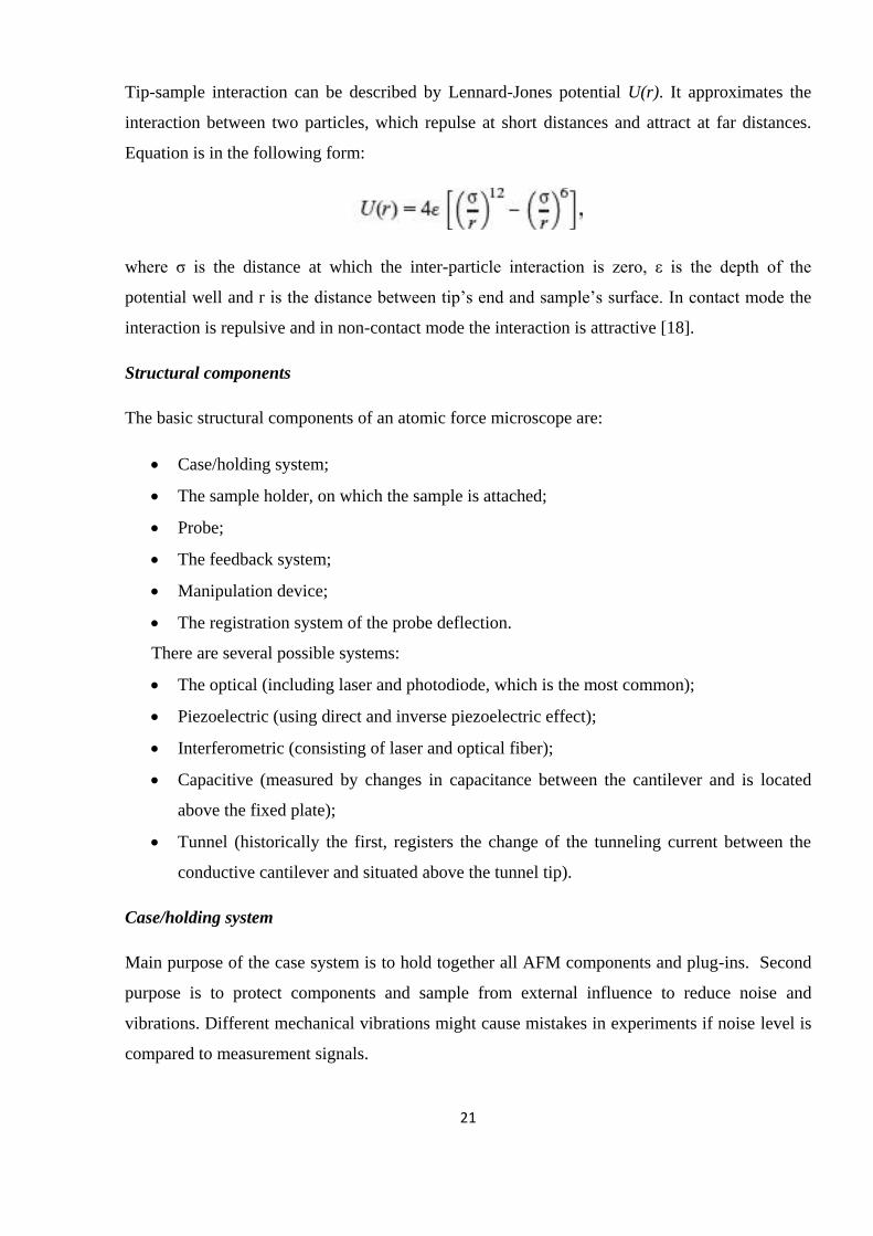
Tip-sample interaction can be described by Lennard-Jones potential U(r). It approximates the
interaction between two particles, which repulse at short distances and attract at far distances.
Equation is in the following form:
where σ is the distance at which the inter-particle interaction is zero, ε is the depth of the
potential well and r is the distance between tip‟s end and sample‟s surface. In contact mode the
interaction is repulsive and in non-contact mode the interaction is attractive [18].
Structural components
The basic structural components of an atomic force microscope are:
Case/holding system;
The sample holder, on which the sample is attached;
Probe;
The feedback system;
Manipulation device;
The registration system of the probe deflection.
There are several possible systems:
The optical (including laser and photodiode, which is the most common);
Piezoelectric (using direct and inverse piezoelectric effect);
Interferometric (consisting of laser and optical fiber);
Capacitive (measured by changes in capacitance between the cantilever and is located
above the fixed plate);
Tunnel (historically the first, registers the change of the tunneling current between the
conductive cantilever and situated above the tunnel tip).
Case/holding system
Main purpose of the case system is to hold together all AFM components and plug-ins. Second
purpose is to protect components and sample from external influence to reduce noise and
vibrations. Different mechanical vibrations might cause mistakes in experiments if noise level is
compared to measurement signals.
Page 22
22
Fig. 13. AFM NTEGRA Prima appearance, picture from official web-site of NT-MDT.
Probe
An AFM probe is a vibrating cantilever with a sharp tip located in one end. Exist variety of
cantilevers for special purposes. Classical cantilever has dimensions of a tens of micrometers
and radius of a tip‟s end in scale of nanometers up to hundred nanometers, depends on
requirements for an experiment. Cantilever is installed in cantilever holder. Cantilever holder, or
holder chip, fits into corresponding holder clip of scanning head of AFM. Scheme of AFM probe
is shown on Fig. 14.
Fig. 14. Scheme of AFM probe.
Page 23
23
AFM probes are usually manufactured by classical planar technology and made of doped silicon
as it is most well-known and cheap material for modern microelectronics. As silicon properties
not always fits properly for demands of measurements, tip or all device might be done from other
material. For example, exists tips made of diamond for scanning some hard samples, or silicon
tip and cantilever might be covered with platinum or gold for studying electrical properties of
specimen. Exist three main characteristics of the tip: first is cantilever resonant frequency w(f);
second is cantilever elastic coefficient kxt; third is tip's apex radius (tip radius) r.
Following information about commercial AFM probes and Figures 15 and 16 are taken from
official web-site of NT-MDT [19].
Substrate:
Substrate is largest part of probe. Cantilever with tip is located on one side of the substrate.
Substrate is jammed in chip holder while scanning process.
Standard chip size: 1.6 x 3.4 x 0.3 mm.
Highly reflective chemically stable Au back side coating (reflectivity is 3 times
better in comparison with uncoated probes).
Compatible with the most of commercial AFM devices.
The base silicon is highly doped to avoid electrostatic charges.
Fig. 15. Substrate [19].
Cantilever:
Page 24
24
Rectangular shape.
Cross-section is trapezium-shape.
Available for contact, semicontact and noncontact modes.
Tip is set on the controlled distance 5-20 мm from the free cantilever end.
Tip:
Total tip shape is tetrahedral, the last 500 nm from tip apex is cylindrical.
Tip height: 14 – 16 мm.
Typical curvature radius:
o of uncoated tips 6 nm, guaranteed 10 nm;
o of coated tips 35 nm.
Tip offset: 5 - 20 мm.
Tip aspect ratio is between 3:1 and 7:1.
Front plane angle: 10° ± 2°.
Back plane angle: 30° ± 2°.
Side angle (half): 18° ± 2°.
Cone angle at the apex: 7° - 10°.
Fig. 16. Tip [19].
Page 25
25
Piezoscanner
Manipulation device is the part of AFM that is moving probe relative to specimen‟s surface. It
consists from mechanic part and piezoelectric scanner. Mechanic part makes rough adjustment
between sample and tip, while piezoelectric scanner is responsible for tip‟s precision engage on
the surface and for scanning sample. Piezoscanner can be explained as piezoelectric tube with 6
electrodes, as shown on Fig. 17, that allow controlling movement of scanner.
Fig. 17. Piezoelectric scanner with x,y and z electrodes [17] .
Piezoscanner is based on reverse piezoelectric effect:
𝑢𝑖𝑗 = 𝑑𝑖𝑗𝑘 · 𝐸𝑘 ,
where uij is strain tensor, Ek is electric field component, dijk are the coefficients of the piezo
coefficient's tensor. Scanner is usually made from piezoelectric ceramics with high piezo
coefficients. Other important demand to scanner material is negligible hysteresis, so direct and
reverse movements should be identic and there is less noise in data signal.
Scanning process is organized by applying a certain electric voltage to electrodes. Planar
movement provided by x and y electrodes and vertical is provided by z electrodes. So there is
possible movement of probe relative to surface in all three (x, y, z) dimensions. Accuracy of
scanner is better than 10-10
m [20].
Page 26
26
3.3. Piezoelectric Force Microscopy
Direct piezoelectric effect means surface charge when applying mechanical stress to the sample.
Phenomenon of mechanical strain of the sample when applying electric field is called reverse
piezoelectric effect. Piezoelectricity can be described by following equations:
P = d*X, (equation A);
S = d*E, (equation B),
where d is the piezoelectric strain coefficient, X is mechanical stress, P is the polarization
charge, S is the ensuing mechanical stress and E is applied electric field. Equation A describes
direct piezoelectric effect. Equation B describes reverse piezoelectric effect [22, 23].
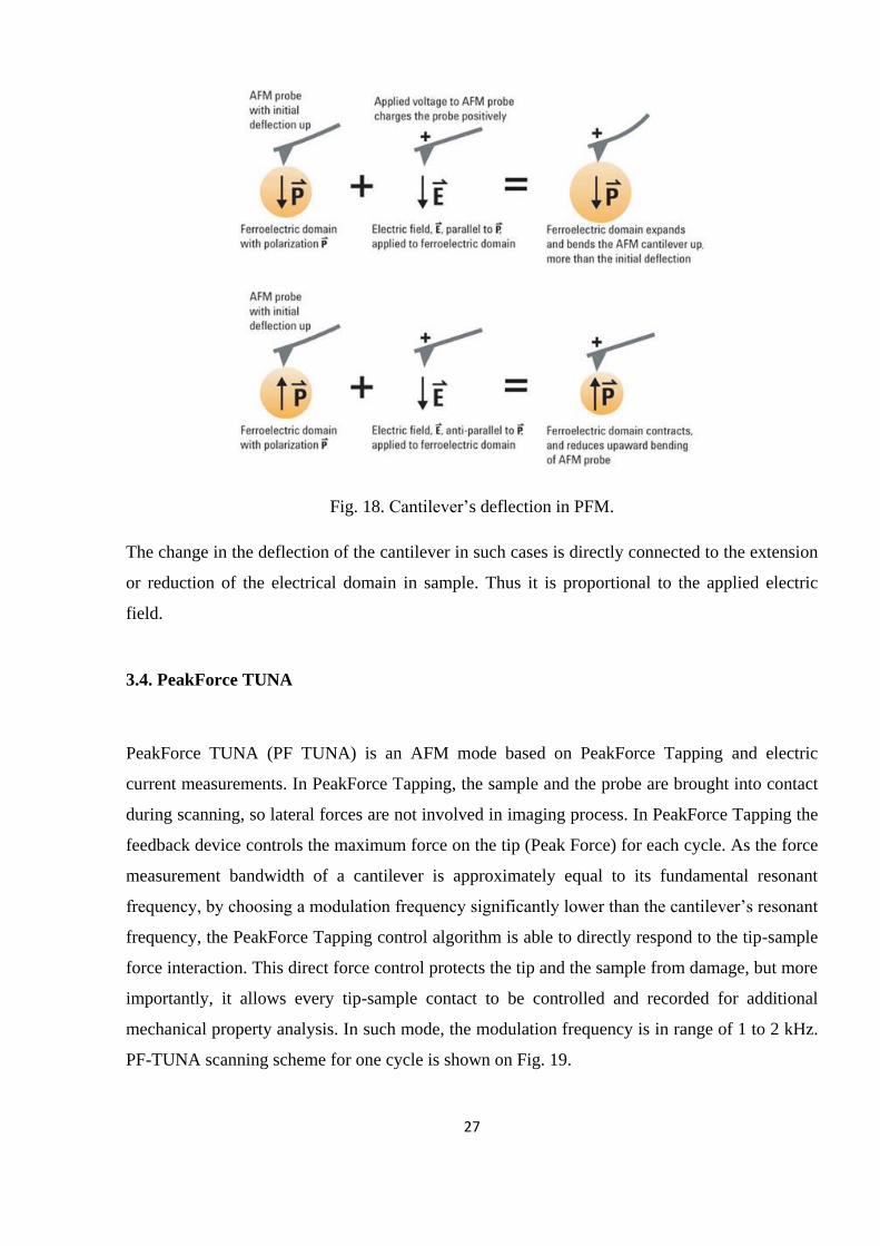
Piezoelectric Force Microscopy (PFM) - is one of the modes of AFM operation that allows
obtaining information about the electromechanical characteristics of different materials. PFM is
based on reverse piezoelectric effect. In the PFM mode the AFM conductive probe comes into
contact with the surface of piezoelectric material. Certain mechanical tension is created inside
the sample by the probe of AFM, thus creating an electric field in the tip-sample contact region.
Due to electrostriction, or reverse piezoelectric effect of investigated materials, the sample
locally expands or shrinks depending on the direction of the external electric field. For example,
if the primary domain of the electric polarization is perpendicular to the sample surface of the
measured sample, parallel to and coincides with the direction of the applied electric field, the
domains will experience a vertical extension. Since the AFM probe comes into contact with the
sample surface, this expansion of domains results upward deflection of AFM cantilever. The
result is an increased deflection of the cantilever compared to that which existed prior to the
application of an electric field. It is opposite situation if the primary domain polarization is
parallel but does not coincide with the direction of the external electric field; the domain will be
compressed, which leads to a decrease in deflection of the cantilever (Fig. 18).
Page 27
27
Fig. 18. Cantilever‟s deflection in PFM.
The change in the deflection of the cantilever in such cases is directly connected to the extension
or reduction of the electrical domain in sample. Thus it is proportional to the applied electric
field.
3.4. PeakForce TUNA
PeakForce TUNA (PF TUNA) is an AFM mode based on PeakForce Tapping and electric
current measurements. In PeakForce Tapping, the sample and the probe are brought into contact
during scanning, so lateral forces are not involved in imaging process. In PeakForce Tapping the
feedback device controls the maximum force on the tip (Peak Force) for each cycle. As the force
measurement bandwidth of a cantilever is approximately equal to its fundamental resonant
frequency, by choosing a modulation frequency significantly lower than the cantilever‟s resonant
frequency, the PeakForce Tapping control algorithm is able to directly respond to the tip-sample
force interaction. This direct force control protects the tip and the sample from damage, but more
importantly, it allows every tip-sample contact to be controlled and recorded for additional
mechanical property analysis. In such mode, the modulation frequency is in range of 1 to 2 kHz.
PF-TUNA scanning scheme for one cycle is shown on Fig. 19.
Page 28
28
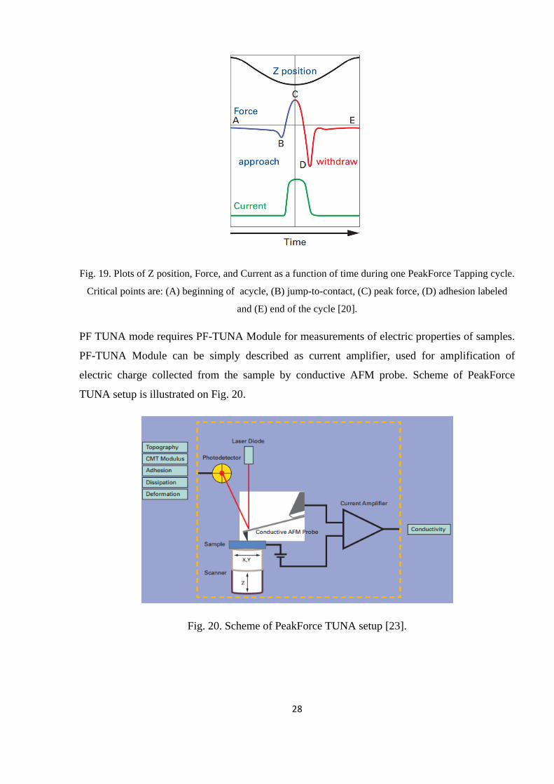
Fig. 19. Plots of Z position, Force, and Current as a function of time during one PeakForce Tapping cycle.
Critical points are: (A) beginning of acycle, (B) jump-to-contact, (C) peak force, (D) adhesion labeled
and (E) end of the cycle [20].
PF TUNA mode requires PF-TUNA Module for measurements of electric properties of samples.
PF-TUNA Module can be simply described as current amplifier, used for amplification of
electric charge collected from the sample by conductive AFM probe. Scheme of PeakForce
TUNA setup is illustrated on Fig. 20.
Fig. 20. Scheme of PeakForce TUNA setup [23].
Page 29
29
PF TUNA can be used for piezoelectric samples investigation, as it gives mechanical and electric
properties while scanning. In the case of PF TUNA use for piezoelectric properties study direct
piezoelectric effect is obtained as we mechanically stress sample and register electric charge
caused by polarization of domains.
3.5. Kelvin mode
Kelvin probe force microscopy (KPFM) is also known as surface potential microscopy. It is a
noncontact variant of AFM. With KPFM, the work function of surfaces can be observed at
atomic or molecular scales. The work function relates to many surface phenomena, including
catalytic activity, reconstruction of surfaces, doping and band-bending of semiconductors, charge
trapping in dielectrics and corrosion. The map of the work function produced by KPFM gives
information about the composition and electronic state of the local structures on the surface of a
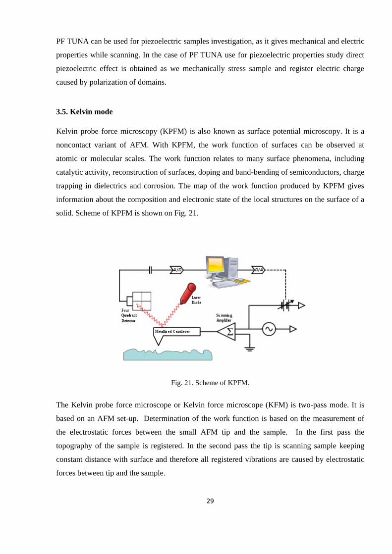
solid. Scheme of KPFM is shown on Fig. 21.
Fig. 21. Scheme of KPFM.
The Kelvin probe force microscope or Kelvin force microscope (KFM) is two-pass mode. It is
based on an AFM set-up. Determination of the work function is based on the measurement of
the electrostatic forces between the small AFM tip and the sample. In the first pass the
topography of the sample is registered. In the second pass the tip is scanning sample keeping
constant distance with surface and therefore all registered vibrations are caused by electrostatic
forces between tip and the sample.
Page 30
30
KPFM is a scanning probe method where the potential offset between a probe tip and a surface
can be measured using the same principle as a macroscopic Kelvin probe. The cantilever in the
AFM is a reference electrode that forms a capacitor with the surface, over which it is scanned
laterally with a constant distance. The conducting tip and the sample are characterized by
different work functions, which represent the difference between the Fermi level and the vacuum
level for each material. If both elements were brought in contact, a net electric current would
flow between them until the Fermi levels were aligned.
Page 31
31
4. Samples
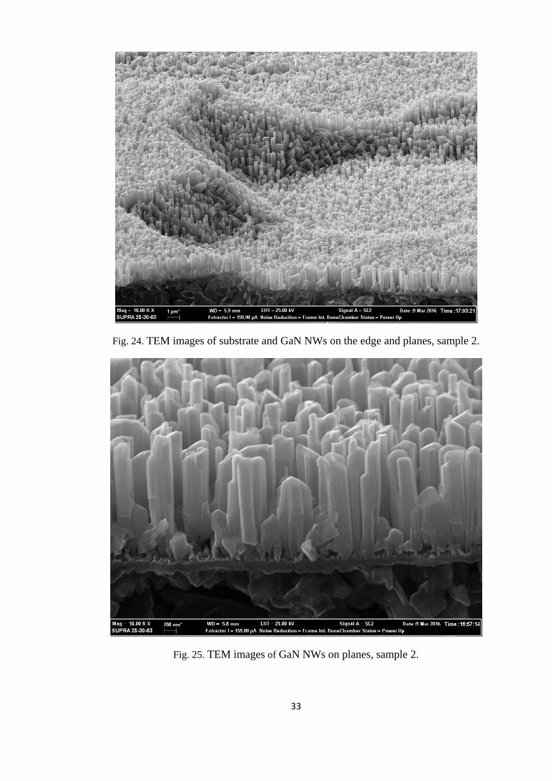
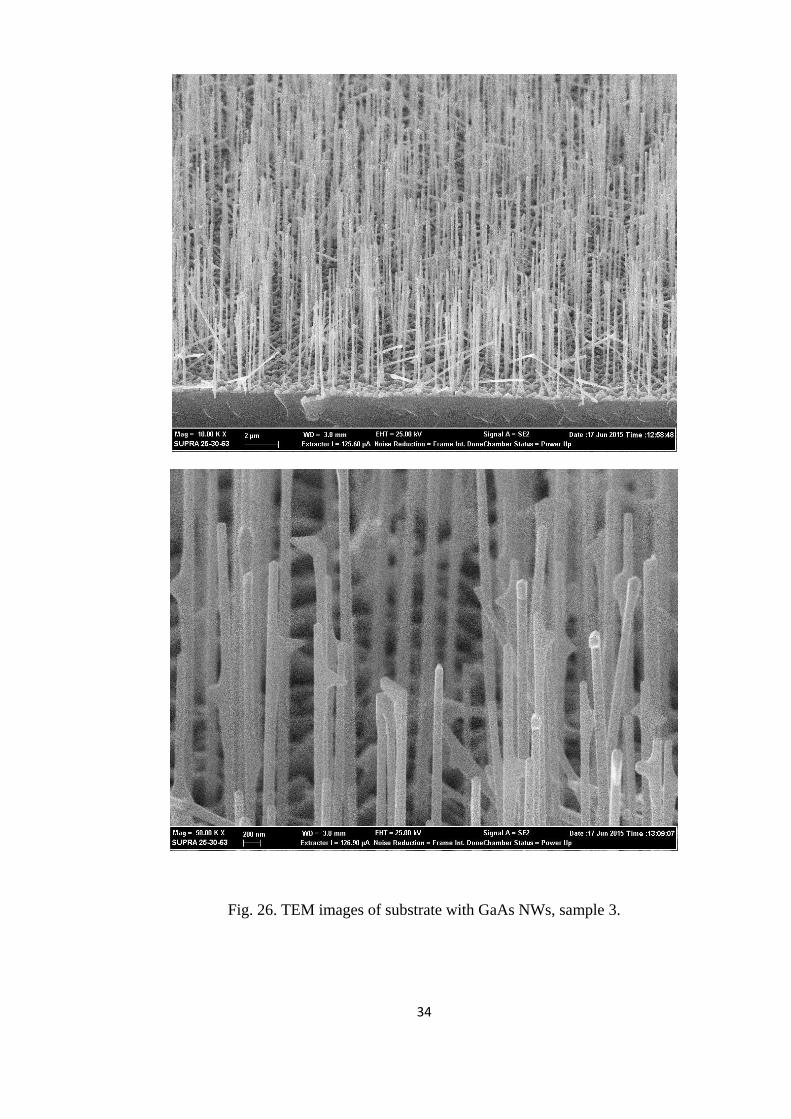
Four different samples were investigated for piezoelectric properties. Samples 1 and 2 with GaN
and sample 3 with GaAs nanowires were manufactured in the Ioffe Institute by MBE. Sample 4
was manufactured in Aalto University. Samples 1, 2 and 3 were visualized by Transmission
Electron Microscopy (Fig.22 and 23 for sample 1, Fig. 24 and 25 for sample 2 and Fig. 26 for
sample 3) prior to AFM experiments. Main properties of samples are listed in Table 1.
Table 1. Samples investigated for piezoelectric properties.
Sample Material Growth
technology
Substrate Diameter,
nm
Length,
µm
Description
Sample 1 GaN MBE Silicon 70-200 1 - 3 Part of nanowires
coalesced together
while growth process.
Sample 2 GaN MBE Silicon 100-300 1 - 3 Nanowires coalesced
during the growth
process, but less than
for sample 1.
Sample 3 GaAs
with
AlGaAs
shell
MBE GaAs 40-100 4 - 5 Nanowires growth
occurs on the silicon
substrate. Mainly
nanowire growth
happened vertically,
but some of them have
certain angle to the
substrate‟s plane
Sample 4 InP VLS Polymorph
Silicon
80-120 4 - 5 Gold droplets with
diameter in order of 10
nm were used as
catalytic agent. Angle
between NWs and
substrate is 22 degrees
Page 32
32
Fig. 22. TEM images of substrate and GaN NWs on the edge, sample 1.
Fig. 23. TEM images of edge with GaN NWs on it, sample 1.
Page 33
33
Fig. 24. TEM images of substrate and GaN NWs on the edge and planes, sample 2.
Fig. 25. TEM images of GaN NWs on planes, sample 2.
Page 34
34
Fig. 26. TEM images of substrate with GaAs NWs, sample 3.
Page 35
35
Fig. 22 – 26 are providing to us information about samples structure, such as length, diameter,
orientation and localization of nanowires. Analyzing the Fig. 22 it is possible to see, that
nanowires, located on the planes of substrate, coalesced together so hard that it is not possible to
identify individual nanowire. There still possible to study individual nanowires on the edges of
substrate. All important results of TEM images are listed in table 1.
Page 36
36
5. Experiments and results
5.1. Measurement sequence
All experiments were done with use of Bruker Multimode 8 atomic-force microscope.
Measurements and data operating was performed with the help of “Nanoscope” software
package.
Device must be turned on in several minutes before experiment.
1. Selection of the probe. Every probe is fabricated for specific purposes. For PFM and PF
TUNA is required conductive probe, such as SCM-PIT. While not in use, probes must be
stored in special box, so environment does not affect them.
2. Loading the probe. The probe is moved from storage with use of tweezers and carefully
installed in special holder of microscope.
3. Setting the sample. The sample roe investigation is placed on a plate and fixed on the
piezotube (it is necessary to avoid damage as tube is fragile) and is electrically grounded.
The measuring head with probe holder is lowered over the sample in distance of 1 - 3 mm
with the help of head's screws to prevent damaging of tip.
4. Laser alignment. Optical microscope is used for configuring laser to the cantilever. Focus
is tuned to the probe. With the help of a laser sensor's screws (or cantilever‟s screws) the
laser spot is introduced to the optical microscope and configured from entering the end
probe. Next step is to select the maximum value of the intensity of the laser with the help
of data on the screen installed to the atomic force microscope. The image of laser spot in
video screen might slightly displace from the probe.
5. Engage. When connecting to AFM via software, exist opportunity to select operation
mode. After selecting required mode, the operator starts the probe approaching to the
surface and enters the necessary parameters for the scanning.
6. Measurements. Measurements setting and data channels must be selected. They can be
changed during scanning the sample or between scannings. Experimental results must be
saved before starting new one.
Page 37
37
7. Handling the data. Usually raw data are not proper for publication, so they must be
additionally handled with use of software, such as Nanoscope Analysis.
5.2 Experiments
Sample 1
GaN nanowires were investigated by PFM. Surface topography (“Height” in Fig. 27), amplitude
in trace and retrace, deflection error channels were registered, providing data while images
obtained with Nanoscope Analysis software are illustrated in Fig. 27.
Fig. 27. Example of images, obtained by scanning sample 1. Amplitude of the AC voltage applied to the
sample was 8Vand mechanical stress was 116 nN.
Page 38
38
In Fig. 18 possible to notice that amplitude signals have same values on trace and retrace, but
trace channel provided more contrasted images. It might be explained by different geometry of
sample-probe contact in trace and retrace directions. Amplitude signal provided us data about
piezoelectric response of the sample. An alternating electric field was applied while scanning the
sample. We registered amplitude of cantilever compiles to vertical geometrical size changes of
the sample investigated. With use of amplitude map, it was possible to calculate vertical
piezoelectric strain coefficient by following equation:
d33 = Aw/Uw,
where d33 is vertical piezoelectric strain coefficient, Aw is medium amplitude of cantilever‟s
vibration on polarized surface and Uw is amplitude of an alternating electric field. Amplitude
maps provide values of Aw in mV. So it is necessary to convert values by multiplying them by
specific coefficient, obtained while calibrating.
Different voltage amplitudes were applied to the same area of the sample during experiment.
That gives an opportunity to estimate precisely vertical piezoelectric strain coefficient, as it is
property of the material and should be independent from applied voltage. Calculated values are
shown in Table 2. Amplitudes are shown on Fig. 27 for scans with no applied voltage and 0.5 V,
5 V and 10 V.
Table 2. Piezoelectric strain coefficient d33 values.
Voltage applied, V. Piezoelectric strain coefficient d33, pC/N.
10 301
8 307
6 306
4 307
2 304
1 307
0,5 301
Piezoelectric strain coefficient value of GaN nanowires of 300 - 310 pC/N, is higher than for
ZnO (12 pC/N), but lower than for PZT (500-600 pC/N).[24]
Page 39
39
Sample 2
PFM
GaN nanowires were investigated by PFM. Surface topography („Height‟), amplitude in trace
and retrace, deflection error channels were registered, providing data and images illustrated in
Fig. 28. Amplitudes of mechanical response were registered for different voltage of the AC signal
applied to the sample.
Fig. 28. Example of images obtained by scanning sample 2. Amplitude of the AC voltage applied to the
sample was 8V for topography image and mechanical stress was 14 nN.
Page 40
40
PF TUNA
GaN nanowires were investigated also by PF TUNA. Surface topography („Height‟) and TUNA
currents in trace and retrace were registered, providing data and images illustrated in Fig. 29.
Fig. 29. Example of images, obtained by the scanning sample 2 with GaN nanowires in PF
TUNA. Bias voltage applied to the sample was 0V, mechanical stress was 3.5 nN.
Piezoelectric strain coefficient d33 of GaN nanowires grown on sample 2 are in the same range as
GaN nanowires grown on sample 1. Differences between values can be explained by different
diameter and distance between neighboring nanowires.
Page 41
41
Results.
Using the data obtained in PFM measurements, piezoelectric strain coefficient d33 was calculated
for sample 2 nanowires. Calculations were done in the same way as for sample 1. Results are
shown n Table 3.
Table 3. Piezoelectric strain coefficient d33 of GaN nanowires, sample 2.
Voltage applied, V. Piezoelectric strain coefficient d33, pC/N.
8 235
5 235
1 235
PF TUNA measurements provided us second proofs of piezoelectric properties of studied
nanowires, as we registered electric currents when tapping sample with no electric field applied.
Part of electric current values are marked in Fig. 29 and they are in range of 15 – 500 pA. Such
scattering of values is well-explained by probe geometry (different area of nanowire-probe
contact), quality of conducting surface, which might be damaged while scanning, and by
different properties of individual nanowires.
Sample 3
GaAs shelled AlGaAs nanowires were investigated by PF TUNA. Individual nanowires were
studied after moving them to conducting substrate to keep them in horizontal position. Surface
topography and cross section of individual nanowire in horizontal position, is shown n Fig 30.
3D Image of single GaAs+AlGaAs shell nanowire shown on Fig. 31. KPFM were used to obtain
data in Fig. 32. Surface topography (Height), TUNA currents in retrace direction for different
level of illumination with no electric field applied were registered, providing data and images
illustrated in Fig. 33.
Page 42
42
Fig.30. Surface topography (upper part) and cross-section (lower part) of individual nanowire
transported to substrate in horizontal orientation.
Fig. 31. 3D Image of single GaAs+AlGaAs shell nanowire.
Page 43
43
Fig.32. Surface potential (upper part) and cross-section of surface potential (lower part) of horizontal
GaAs+AlGaAs shell nanowire, measured by KPFM.
Surface potential of nanowire is different from potential of substrate. Also exists difference in
potential values between areas of nanowire with different diameter, so that might be proof of
multiphase in nanowire. Most probably, those are wurtzite and zink-blend phases. Nanowire was
glued to substrate by drop of acid, that might cause changes in structure.
Fig. 33. Sample 3, Height and retrace TUNA currents of GaAs shelled AlGaAs nanowires.
Page 44
44
Electric current peaks with zero applied voltage show that the sample has direct piezoelectric effect.
Electric currents are registered on the top of nanowires. Dispositions might be explained by probe
geometry and lack of conducting layer on the tip.
Fig. 34. Sample 3, retrace TUNA currents of GaAs shelled AlGaAs nanowires with additional
illumination and in the dark ambient.
Similar measurements were carried out in the absence of illumination and its larger significance.
In the dark ambient environment more noise was registered. Since the currents map matches,
despite of the noise, we can conclude that piezoelectric response was registered.
Samples might be scanned not only by tip, but also with cantilever. Considering that the area of
contact is bigger when scanning sample with cantilever, it is possible to register electric currents
even if the conducting cover of the tip is damaged. Example of such scan is shown in Fig. 35. As
we registered electric currents while bending nanowire both with tip and with cantilever with no
electric field applied, direct piezoelectric response was obtained on this sample. Such topography
is explained by probe convolution on the sample. Initially cantilever is bending nanowire and
after the tip is also bending nanowire, registering topography and electric current.
Page 45
45
Fig. 35. GaAs shelled AlGaAs nanowire scanned both by tip and cantilever in PF TUNA mode.
Sample 4
InP nanowire were investigated by PF TUNA. Surface topography and electric currents in trace
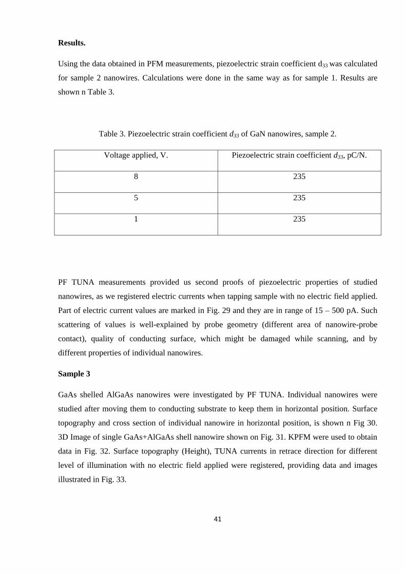
and retrace are shown in Fig. 36 and 37.
Fig. 36. Topography of InP nanowires.
Page 46
46
Fig. 37. Tuna Currents of InP nanowires with Amplitude of the DC voltage applied to the sample 2 V.
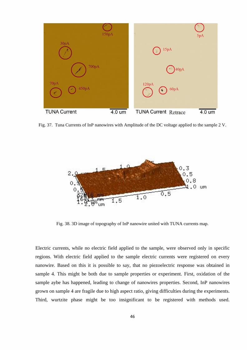
Fig. 38. 3D image of topography of InP nanowire united with TUNA currents map.
Electric currents, while no electric field applied to the sample, were observed only in specific
regions. With electric field applied to the sample electric currents were registered on every
nanowire. Based on this it is possible to say, that no piezoelectric response was obtained in
sample 4. This might be both due to sample properties or experiment. First, oxidation of the
sample aybe has happened, leading to change of nanowires properties. Second, InP nanowires
grown on sample 4 are fragile due to high aspect ratio, giving difficulties during the experiments.
Third, wurtzite phase might be too insignificant to be registered with methods used.
Page 47
47
Conclusions
1) PFM measurements of sample 1 with GaN nanowire have shown reverse piezoelectric
effect on studied structure. Based on gained data, piezoelectric strain coefficient d33 of
GaN nanowires was calculated.
2) PFM and PF TUNA measurements of GaN sample #2 showed both reverse and direct
piezoelectric effect. Based on obtained data, piezoelectric strain coefficient d33 of GaN
nanowires was calculated.
3) GaAs nanowires of sample #3 were measured by KPFM and PF TUNA. KPFM of
nanowires showed that the contact potential is different on the cross-section of nanowire,
but sample without acid treatment is required for further experiments. PF TUNA
measurements proved existence of direct piezoelectric response. Photovoltaic influence
was investigated. It showed that reducing of amount of light, falling to the sample, leads
to increase of noise level.
4) The experiment of sample 4 failed to prove existence of any piezoelectric properties in
InP nanowires.
5) The experiments provide enough data to conclude, that GaN nanowires can be used both
for generating electricity and for transducing electricity into mechanical work, so
nanogenerators can be produced of them as well as nanoengines and nanosensors.
6) GaAs and InP nanowires should be additionally studied by KPFM to determine role of
different crystal phase in piezoelectric properties of nanowires.
Page 48
48
Summary
In this work A3B5 InP, GaAs and GaN nanowires were investigated for piezoelectric properties
by using PFM and PF TUNA modes of AFM. In addition, KPFM mode was used for
investigating crystal structure of nanowires. Topography, amplitude, surface potential and
TUNA currents maps are presented in high-resolution AFM images. All samples were
investigated with Bruker Multimode 8 AFM.
The main highlights of this work can be established:
1) Piezoelectric properties were obtained for GaN and GaAs nanowires. Two different
methods, PFM and PF TUNA, were used for investigation of piezoelectric properties of
nanowires. Direct and reverse piezoelectric effects were registered.
2) Piezoelectric strain coefficients d33 of GaN nanowires were calculated for samples 1 and
2. For sample 1 piezoelectric strain coefficient d33 is 305 pC/N, for sample 2 d33 is 235
pC/N.
3) Procedure of SPM experiment to measure the piezo response of vertical 1D structures
and calculation of the piezo coefficient was developed.
Difference between d33 values for GaN nanowires of sample 1 and sample 2 is connected
with their different properties, such as diameter and order on the substrate. Still, calculated
coefficients are in the same range. Such big d33 values are in agreement with coefficients of
other nanowires with good piezoelectric properies.
Piezoelectric properties of studied GaN and GaAs nanowires can be utilized for various
purposes, such as sensors, electricity generators and nanodrives. GaAs is often used in Solar
energy harvesting, so it could find use in new type of generators, based on producing
electricity both from light and mechanical vibrations.
Following requirements are elaborated for the samples:
1) Nanowires should be grown in such a way, that distance between them will provide
opportunity to measure individual nanowire.
Page 49
49
2) Height of nanowires should be in order of 500 nm, so they wold not be so fragile. It can
be made, for example, by growing short nanowires, or by fulfilling space between them
by polymer.
3) If nanowires are turned from vertical to horizontal orientation, they must be glued to
substrate carefully to prevent their pollution and degradation.
4) Only one parameter must be changing in one series of samples, so it is possible to make
conclusion about influence of that parameter on the properties.
5) Sample with-known and easily detected properties can be used as comparison sample for
easier setting of further experiments.
Based on these results, few possible ideas for future investigation can be named:
1) Study of crystal structures of nanowires surface by electric potential behavior using
KPFM measurements.
2) Study of lateral piezo response of A3B5 nanowires by PFM and PF TUNA modes.
3) Study of influence of passivation layers of different materials on following properties of
nanowires: piezoelectric, conducting and mechanical properties and degradation of
nanowires.
4) Influence of doping on electromechanical properties of nanowires.
These studies can provide fundamental value and can be used to improve the existing technology
or to create new type of functional devise.
Page 50
50
References
[1] Amy E. Marquardt et al., Protecting silver cultural heritage objects with atomic layer
deposited corrosion barriers, Heritage Science, 2015.
[2] Han-Bo-Ram Lee et al., Growth of Pt Nanowires by Atomic Layer Deposition on Highly
Ordered Pyrolytic Graphite, Nano Lett., 2013, 13 (2), pp 457–463.
[3] S. Noor Mohammad, Analysis of the Vapor–Liquid–Solid Mechanism for Nanowire Growth
and a Model for this Mechanism, Nano Lett., 2008, 8 (5), pp 1532–1538.
[4] Lin Chen et al., Semiconductor Nanowire Growth and Integration, 2014, pp. 1-53.
[5] Heon-Jin Choi, Semiconductor Nanostructures for Optoelectronic Devices, NanoScience and
Technology, 2012.
[6] R. Adelung, et al., Strain-controlled growth of nanowires within thin-film cracks, Nature
Materials, 2004.
[7] A. Gustafsson et al., Low pressure organometallic chemical vapor deposition of quantum
wires on V-grooved substrates, Applied Physics Letters, 1995.
[8] T Schumann et al, Nanotechnology, 2011
[9] Jaeger, Richard C., Film Deposition. Introduction to Microelectronic Fabrication (2nd ed.).
Upper Saddle River: Prentice Hall, 2002
[10] Y. Tao et al., Single-Crystal Diamond Nanowire Tips for Ultrasensitive Force Microscopy,
Nano Lett., 2015, 15 (12), pp 7893–7897.
[11] M. Heiss et al., Self-assembled quantum dots in a nanowire system for quantum photonics,
Nature Materials, 2012, 439–444.
[12] Pv News November 2012. Greentech Media, 2012.
[13] Letian Dou et al., Solution-Processed Copper/Reduced-Graphene-Oxide Core/Shell
Nanowire Transparent conductors, ACS Nano, 2016, 10 (2), pp 2600–2606.
[14] http://phys.org/news/2016-04-chemists-battery-technology-off-the-charts-capacity.html
Page 51
51
[15] Garret Moddel and Sachit Grover, rectenna solar cells, 2013.
[16] Zhong Lin Wang et al., Piezoelectric Nanogenerators for Self-Powered Nanodevices,
PERVASIVE computing, 2008
[17] G. Binnig et al., Atomic Force Microscope, Phys. Rev. Lett.,1986
[18] Di Pierro et al., A Stochastic Algorithm for the Isobaric-Isothermal Ensemble with Ewald
Summations for all Long Range Forces, Journal of Chemical Theory and Computation, 2015
[19] Web-site of NT-MDT corparation. http://www.ntmdt-tips.com/text/general-information
[20] V.Mironov, Fundamentals of Scanning Probe Microscopy, N.Novgorod, 2004 (in Russian)
[21 ] NT-MDT Ntegra Aura User Manual.
[22] Piezoelectric Transducers and Applications, A. Arnau, Editor, Springer-Verlag Berlin Heidelberg,
2004.
[23] Simultaneous Electrical and Mechanical Property Mapping at the Nanoscale with PeakForce TUNA,
BRUKER‟s Application Note #132.
[24] Joe Briscoe,Steve Dunn, Nanostructured Piezoelectric Energy Harvesters, 2014.