Follow this and additional works at: https://ir.lib.uwo.ca/etd
Part of the Power and Energy Commons, Signal Processing Commons, and the VLSI and Circuits,
Embedded and Hardware Systems Commons
Recommended Citation Recommended Citation Lele, Sneha Arun, "Piezoelectric Transformer and Hall-Effect Based Sensing and Disturbance Monitoring Methodology for High-Voltage Power Supply Lines" (2013). Electronic Thesis and Dissertation Repository. 1618. https://ir.lib.uwo.ca/etd/1618
This Dissertation/Thesis is brought to you for free and open access by Scholarship@Western. It has been accepted for inclusion in Electronic Thesis and Dissertation Repository by an authorized administrator of Scholarship@Western. For more information, please contact [email protected].
4.2 Orthogonal polarizations in input and output sections of PT. . . . . . . . . . . . 424.3 Free tetrahedral meshing applied to COMS OL PT model. . . . . . . . . . . . . 424.4 3D plots for PT displacement (volume deformation) in nm at eigen frequencies
14.79kHz, 40.71kHz, 75.62kHz, 120.57kHz, 168.05kHz and 209.04kHz . . . . 444.5 3D plots for PT displacement in nm (top) and output potential in V (bottom) at
resonance . . . . . . . . . . . . . . . . . . . . . . . . . . . . . . . . . . . . . 454.6 Simulated susceptance at the output terminal of PT model at main resonant
frequency and at second harmonic frequency. . . . . . . . . . . . . . . . . . . 464.7 Simulated frequency response of PT model showing main resonance and sec-
ond harmonic frequency (top), low frequency response (bottom) with 10MΩ
4.9 Typical types of faults in a 3Φ power system. . . . . . . . . . . . . . . . . . . 494.10 Time–domain PS CAD generated voltage signal applied to PT model as input. . 504.11 Stepped down output voltage of PT model for high voltage time–domain input
applied . . . . . . . . . . . . . . . . . . . . . . . . . . . . . . . . . . . . . . . 504.12 Simulated phase delay between input to PT model and output recorded for that
input for 60Hz component. . . . . . . . . . . . . . . . . . . . . . . . . . . . . 514.13 Simulated phase delay between input to PT model and output recorded for that
input for high frequency component. . . . . . . . . . . . . . . . . . . . . . . . 524.14 Photo of input and output connections for single–ended PT. . . . . . . . . . . . 544.15 PT configurations: Single ended connection (left), differential connection (right) 554.16 Experimental set–up for measurements with real–time input signals. . . . . . . 564.17 Most recent experimental set–up for measurements with real–time input signals. 574.18 Experimentally recorded frequency response showing main resonance and sec-
ond harmonic frequency (top), low frequency response (bottom) with no loadcondition for varying input voltage. . . . . . . . . . . . . . . . . . . . . . . . . 58
4.19 Experimentally recorded low frequency response for 100Vrms input overlappedwith results of the fitting linear function of the form y = ax+b (top), percentageerror between measured output and fitted data (bottom). . . . . . . . . . . . . . 59
4.20 Experimentally recorded low frequency response for 100Vrms input using aregular BNC compared with passive probe demonstrating loading effect. . . . . 60
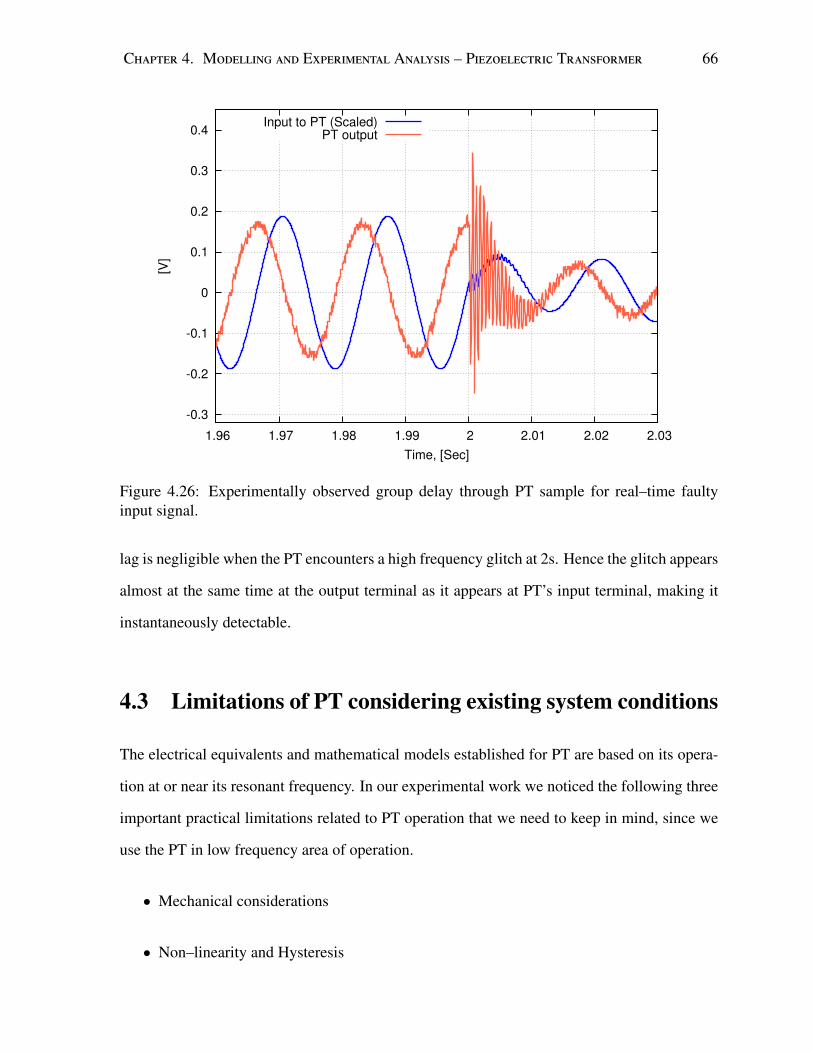
4.22 Schematic diagram for PS CAD case 1 power system simulation model example. 634.23 Schematic diagram for PS CAD case 2 power system simulation model example. 634.24 Stepped down PT output voltage for high power input applied experimentally . 644.25 Experimentally measured group delay through PT sample for varying frequen-
input signal. . . . . . . . . . . . . . . . . . . . . . . . . . . . . . . . . . . . . 664.27 Photo of a PT size compared to a Canadian penny, held using cellophane tape
(left), PT clamped on to a PCB using a cable tie (right). . . . . . . . . . . . . . 674.28 Negligible hysteresis observed during experimental measurements at power–
5.1 Photo of development kit used for measurements based on IMC MLX91205 ICand its 3D rendering showing narrow conductor width under the IC . . . . . . . 75
5.2 3D COMS OL model representing the Hall–effect based IMC concept showingthe conductor with lateral Hall elements and two hexagonal magnetic concen-trators. . . . . . . . . . . . . . . . . . . . . . . . . . . . . . . . . . . . . . . . 76
5.3 Simulated effect of varying width of the part of the conductor under the Hallelements, on normal magnetic flux density distribution in the COMS OL model. 77
viii
5.4 Simulated z component of magnetic flux density variation observed betweenthe hexagonal concentrators along the two facing boundaries in the model. . . . 78
5.5 Time–domain plot of secondary current exported from PS CAD power systemmodel applied to Hall model in COMS OL, for fault and no fault condition. . . 79
5.6 Time–domain plot of z component of magnetic flux density recorded on con-centrator boundaries facing each other in the gap, for time varying input current. 80
5.7 Schematic diagram of direct single–ended connection for the open loop MLXcurrent sensor. . . . . . . . . . . . . . . . . . . . . . . . . . . . . . . . . . . . 81
5.8 Experimentally recorded MLX output voltage for increasing current, flux varia-tion with current in COMS OL model representation (top), Experimental MLXfrequency response, recorded flux change with frequency in COMS OL Hallmodel representation, for 1A and 5A (bottom). . . . . . . . . . . . . . . . . . . 82
6.1 Block diagram of a signal flow representation showing steps involved in sens-ing, processing and decision making process in a digital relay. . . . . . . . . . 86
6.2 Frequency spectrum of experimentally recorded piezo outputs for case 1 faultcondition. . . . . . . . . . . . . . . . . . . . . . . . . . . . . . . . . . . . . . 89
6.3 Frequency spectrum of experimentally recorded piezo outputs for case 2 faultcondition. . . . . . . . . . . . . . . . . . . . . . . . . . . . . . . . . . . . . . 90
6.4 Frequency spectrum of simulated piezo outputs for case 2 fault condition. . . . 916.5 Zoom–in frequency spectrum of 1710Hz centred BP filter for case 2 fault con-
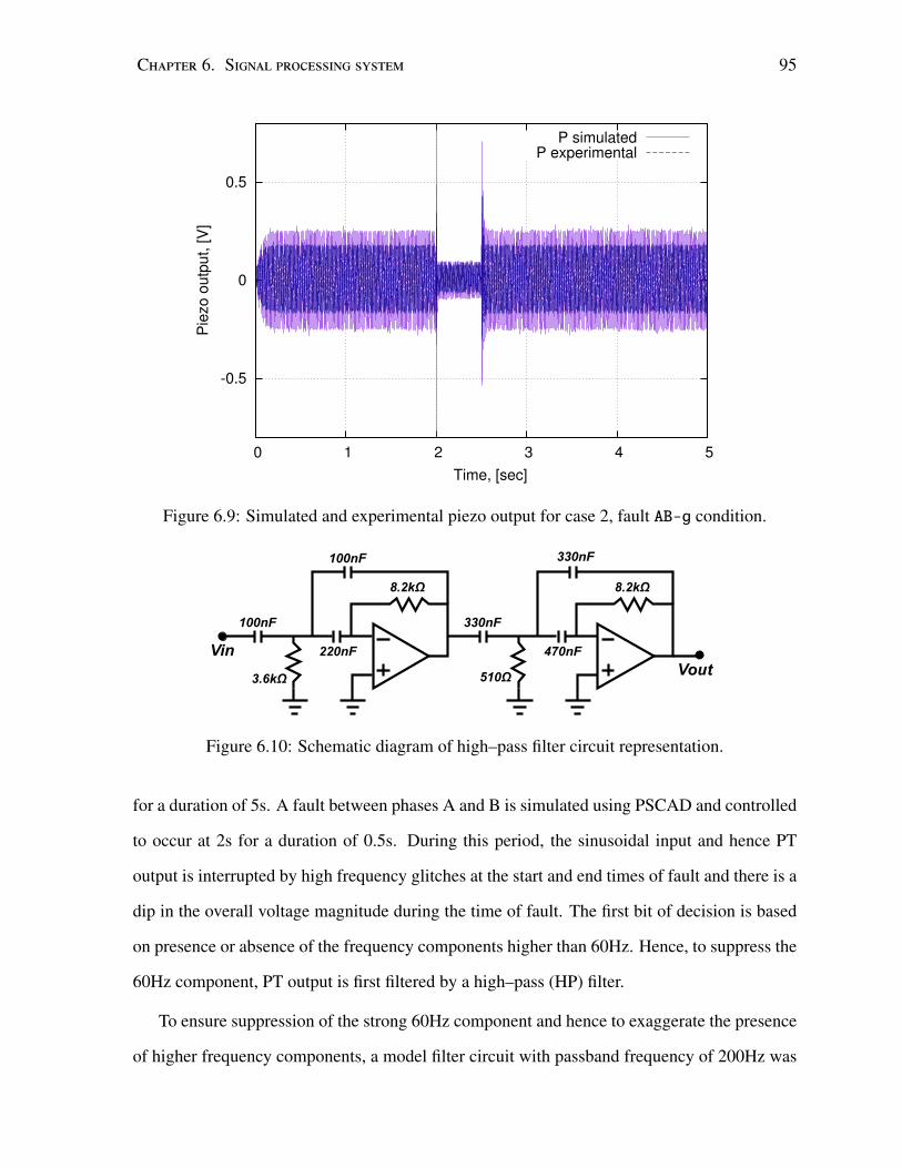
dition, simulated (left) and experimentally recorded (right). . . . . . . . . . . . 926.6 Truth table of decision making system . . . . . . . . . . . . . . . . . . . . . . 936.7 Behavioural block diagram of the decision making system. . . . . . . . . . . . 946.8 Behavioural block diagram of the signal processing system. . . . . . . . . . . . 946.9 Simulated and experimental piezo output for case 2, fault AB-g condition. . . . 956.10 Schematic diagram of high–pass filter circuit representation. . . . . . . . . . . 956.11 Simulated and experimental piezo output for case 2 (zoomed near fault region),
fault AB-g condition (top), HP filtered output (bottom). . . . . . . . . . . . . . 966.12 Schematic diagram of peak detector circuit based on the “ideal diode” circuit. . 976.13 Time domain peak detector output signal (top), comparator output signal (bot-
tom) for first bit of information (bit 1). . . . . . . . . . . . . . . . . . . . . . 986.14 Time–domain plots of positive and negative comparator waveforms and corre-
sponding AND gate decision signal during start of fault (top) and end of fault(bottom). . . . . . . . . . . . . . . . . . . . . . . . . . . . . . . . . . . . . . . 100
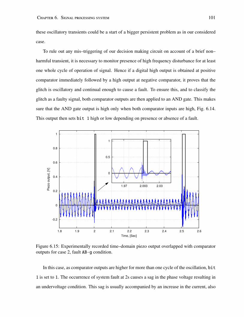
6.15 Experimentally recorded time–domain piezo output overlapped with compara-tor outputs for case 2, fault AB-g condition. . . . . . . . . . . . . . . . . . . . 101
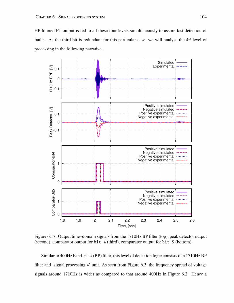
6.16 Frequency spectrum of original PT output for fault AB-g, case 2 and PT outputfor no–fault condition, overlapped with output after being treated with HP and1710Hz BP filter, simulated (top) and experimentally recorded (bottom). . . . . 103
4.1 Properties of PT type C–205 used in modelling . . . . . . . . . . . . . . . . . 434.2 Effect of length of PT (l) on resonant frequency ( fR) and on low frequency
This chapter introduces the background of the research documented in this thesis. An overview
of a typical relay system, its evolution and the existing technologies driving this system are
discussed here. The motivation behind the solutions explored in this thesis, scope of the work
and finally the outline of this thesis follow in this chapter.
1.1 Overview
Relays have been used in the power industry for more than 100 years for purposes of distur-
bance detection in power systems and isolation of fault–causing component. The first relay
installations made by companies like GE and ABB in early 1900s [1] were of electromechan-
ical type, based on simple induction principles to provide protection to power systems. As an
effort towards integration, this technology was then followed by the emergence of solid–state
relays. These relays offered advantages like high speed, increased lifetime and high space effi-
ciency over electromechanical relays. As solid–state relays appeared to have established in the
protection area, digital–based relaying was first contemplated during the late 1960s. The idea
that all the power system equipment in a substation could be protected using digital computers
has ever since led to ongoing research in digital protection.
Microprocessor–based relays were first introduced in 1980s [2]. Since then, the rapid evo-
1
Chapter 1. Introduction 2
lution that microprocessor technologies underwent, encouraged the growth of these relays in
power industry. Not only do microprocessor–based relays combine most of the functions of
several components of electromechanical and solid–state relays, but also provide features like
programmable logic, real–time metering and ability to communicate with processors of other
relays, that were not available in the older technologies [3]. The main advantages that digital
protection has over conventional methods are [4] listed below.
1. Reliability of a system depends on the following characteristics of a power system [5],
(a) Capacity to perform within acceptable limits during normal operation;
(b) Capacity to limit the scope and impact of failures if any;
(c) Ability to restore integrity promptly if lost;
(d) Ability to supply continuous power taking into account both scheduled and un-
scheduled outages.
Features like self–monitoring and built–in redundancy in digital relays ensure improved
reliability. The NERC 2012 State of Reliability report suggests a stable bulk power
system reliability for the period 2008 to 2011. The advances in power system protection
have ensured that the bulk power system is within the defined acceptable adequate level
of reliability (ALR) conditions.
2. Adaptability of digital relays due to the fact that they are programmable and have an
extensible design architecture, makes it possible to use the same relay for more than one
function.
3. Cost involved in relay systems has substantially reduced due to advancement in inte-
grated technology and high volume production. On the other hand, cost of conventional
relays has continued to increase due to outdated technologies and high maintenance.
4. Performance and other features like post–fault analysis capabilities and increased ac-
curacy in fault–location methods have no parallel in conventional technologies.
Chapter 1. Introduction 3
Power substationPower substation
Processor
Memory Communication Power supply
Digital
inputs
Analogue
V & I inputs
Digital
outputs
Signal processing
& sampling
Microprocessor-based relay system
Figure 1.1: Block diagram of a typical microprocessor–based relay system used in power dis-tribution substations.
A typical microprocessor–based relay system, Fig. 1.1, consists of sub–circuits that in-
terface with the secondary signals in high–power application environment and convert high
energy signals into low energy signals. The analogue sub–systems reduce the levels of input
signals, these signals are then converted to digital signals after signal conditioning. These low
energy isolated digital signals are then fed directly to processors and their peripherals. The
relay algorithms process this acquired information and send digital commands for smooth op-
eration of the entire system [3]. Even though well–established designs for sub–circuits that
drive these relays exist, there is need for improved technology with respect to size, efficiency
and reliability.
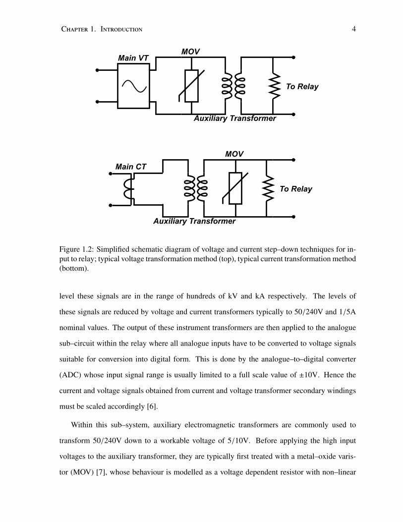
Apart from digital inputs to relay that indicate contact status, two main types of analogue
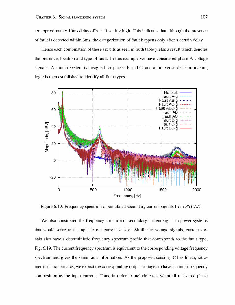
inputs to the power relay hardware are AC voltage and AC current inputs. At the power system
Chapter 1. Introduction 4
Main VTMOV
Auxiliary Transformer
To Relay
Main CT
MOV
Auxiliary Transformer
To Relay
Figure 1.2: Simplified schematic diagram of voltage and current step–down techniques for in-put to relay; typical voltage transformation method (top), typical current transformation method(bottom).
level these signals are in the range of hundreds of kV and kA respectively. The levels of
these signals are reduced by voltage and current transformers typically to 50/240V and 1/5A
nominal values. The output of these instrument transformers are then applied to the analogue
sub–circuit within the relay where all analogue inputs have to be converted to voltage signals
suitable for conversion into digital form. This is done by the analogue–to–digital converter
(ADC) whose input signal range is usually limited to a full scale value of ±10V. Hence the
current and voltage signals obtained from current and voltage transformer secondary windings
must be scaled accordingly [6].
Within this sub–system, auxiliary electromagnetic transformers are commonly used to
transform 50/240V down to a workable voltage of 5/10V. Before applying the high input
voltages to the auxiliary transformer, they are typically first treated with a metal–oxide varis-
tor (MOV) [7], whose behaviour is modelled as a voltage dependent resistor with non–linear
Chapter 1. Introduction 5
voltage–current characteristics, used to protect circuits against excessive transient voltages.
Figure 1.2 (top) shows a typical existing voltage transformation technique.
For metering purposes, current inputs must be converted to voltages, for example by resis-
tive shunts. As the current transformer secondary may be as high as hundreds of amperes in
normal operating conditions, shunts of resistance of few mΩ are needed to produce the desired
level of input voltage for the ADCs. One alternative is to use an auxiliary current transformer.
However, any inaccuracies in transformer would propagate and result in total error in the con-
version process, which must be kept as low as possible. One advantage of using a transformer
is that it provides electrical isolation between main CT secondary and digital computer system.
After the step down of high AC currents to 1/5A, the current is converted to a voltage for com-
patibility with the ADC. Figure 1.2 (bottom) shows a typical existing current transformation
technique. These signals containing information about power line voltages and currents are
then subjected to pre–filtering, sampling and finally to an ADC and the processing circuit.
Research has been done in areas of voltage and current metering and instrumentation on
high power side of relay systems and on signal processing end of the system. Recently used
technique which consists of a primary current sensing system based on an optically interrogated
mechanism devised by GE, Global Research [8] allows for multiplexing of more than one
monitoring channel.
Other innovations, such as monitoring system based on optical fibres in combination with
a laser diode and photo–voltaic cell [9], have shown to be safe and reliable alternatives to
metallic lines that transmit sensor signals.
In a typical power system, analogue current is periodically sampled and converted to dig-
ital data for analysis and to facilitate monitoring and detection of faults. In [10], the authors
discuss an improved monitoring system which samples analogue signals at a rate higher than
128 samples per second, to capture those high–speed transients which cannot be detected by
conventional sampling techniques.
Resistive current sensors, Rogowski coils based on Faraday’s law of induction, magnetic
Chapter 1. Introduction 6
field sensors, and current sensors based on Faraday’s effect, are few of the principles estab-
lished and implemented in commercial and industrial applications for current sensing [11, 12].
Optical current sensors are gaining high acceptance in power system applications, [13], due to
their high accuracy, high bandwidth and inherent isolation property as compared to the above
mentioned sensors. An electro–optic, hybrid current sensing technique which uses a combina-
tion of Rogowski coil and optical fibre cable in [14] presents a current measurement instrument
for high–voltage power lines.
However, so far, to the best of our knowledge, there have been no reported alternatives
suggested for electromagnetic transformer in low power side of relay system for voltage mea-
surement and step–down. Similarly, in this particular area of application, there have been no
suggested alternatives for current metering other than the conventional resistor based method.
1.2 Scope, objective and contributions of the thesis
The main objective of this work is to develop a method that may enable the replacement of
existing sensing devices on the low power side of relay system, with alternatives that meet
requirements of electrical isolation, accuracy, exact reproduction of the primary signal and
least delay time as the signal travels from input to output. In our proposed methodology we
use a piezoelectric transformer (PT) in its low frequency region of operation for voltage sensing
and step–down and a Hall–effect based sensor for current sensing and metering.
The existing voltage sensing mechanism makes use of the conventional magnetic trans-
formers in a board based design. These transformers consist of a winding, and considering the
large number of analogue input subsystems that include these transformers, in a single sub-
station, presence of these windings increases space occupancy and cost of manufacturing of
the transformer. The magnetics of the transformer also leads to problems like electromagnetic
interference (EMI) and potential short circuit hazards.
Use of PTs as an alternative to conventional magnetic transformers to achieve efficient
Chapter 1. Introduction 7
Current inCurrent out
Digital inputs to relay
Power lines
1A or 5A
Piezo
set-up
50 to 240V
VoutVout
(proportional to
current value)
Relay system
Signal processing and
amplification
Hall-effect
sensor
ABC
Figure 1.3: Block diagram of the proposed signal monitoring system.
and integrated electrical isolation has been explored since 1950s due to its advantages, e.g.
low cost, high efficiency, high operating frequency, good input–output isolation [15], no EMI
and no potential short–circuit fire hazard [16]. PTs have been typically used in cold cathode
lamps, notebook computers, camera flash and some of the most compact high voltage sources.
They exhibit high power density [17] and vibration frequency is the resonant frequency of
piezoceramic block in 100kHz to 1MHz range. Reported applications of PT operating at its
fundamental resonant frequency also include power converters [18] and gate–driver circuits
[19]. A method to drive PT with a square waveform of frequency lower than the resonant
frequency but which contains PT’s resonant harmonic is presented in [20]. However there are
no reported applications of PT in its low frequency region of operation, neither have methods
to drive PT directly with power–line frequency signals been discussed before.
In our initial experiments we used a commercially available piezoceramic transformer to
Chapter 1. Introduction 8
characterize its resonant and low–frequency behaviour. However, in order to develop a stan-
dardized voltage transformation system, a large number of PTs would be required to be anal-
ysed with respect to their size, physical and material properties, which was not practical in
our study. Instead, finite element modelling (FEM) proves to be a very useful method for
behavioural analysis in order to encompass a large sample set of PTs.
The other aspect of the objective is to propose a feasible alternative to replace the existing
resistive current sensing methodology. The existing current metering in the analogue input
subsystem is done by the transformer–resistor combination. Use of resistors to convert the
current to a voltage leads to resistive losses and measurement errors. The growing need of a
safe, isolated and low loss current detection technique has led to development of non–intrusive,
non–resistive current sensing methods and devices [12]. Here, we explore the Hall–effect based
current sensor based on the concept of integrated magnetic concentrator (IMC), to implement
a resistor–free current sensing technique. A Hall–based sensor combines advantages of both,
a transformer, by providing electrical isolation between high and low energy sides of a circuit
and that of a resistor, by providing a robust and cheap way to convert the sensed current into a
voltage equivalent. An analysis of a commercial current sensor supported by 3D modelling of
the principle of integrated magnetic concentrator and Hall–effect shows a long–term potential
to perform better than the shunt–based techniques currently used.
In the system proposed here, the scaled down voltage and current signals are passed through
a signal processing system which consists of filters, peak detector circuit and comparator cir-
cuit, developed in order to detect the disturbance with minimum delay and help differentiate
between the non–faulty and faulty signals. Finally, a combined sensing system which incorpo-
rates both voltage and current metering and signal processing sub–systems for all phases in a
power system is proposed, Fig. 1.3.
Chapter 1. Introduction 9
1.3 Organization of the thesis
This thesis is structured in the following order:
In chapter 2, an overview of PT, its history and operational principle is discussed. The
discussion then presents a mathematical analysis of direct and inverse piezoelectric effect. The
electrical model is also briefly discussed in this chapter.
Chapter 3, gives an overview of the different methods used presently in industry and elec-
tronic applications for current sensing and metering. The concept of integrated magnetic con-
centrator is discussed and Hall–based commercial sensor used in our work is introduced.
Chapter 4 explains the modelling of PT in COMSOL based on the mathematical under-
standing of PT operation. This is followed by a discussion about PT eigen frequency analysis,
frequency domain analysis and time domain analysis with simulation results. A section which
presents results of all the experimental measurements carried out, the different PT configura-
tions used, effect of load and high frequency transients and finally limitations involved in use
of PT is also included in this chapter.
Chapter 5 discusses the nature of current inputs to relay system in normal and faulty con-
ditions and presents a numerical model for Hall sensing principle. The simulated results are
compared in trend with the actual measurements obtained from the commercial Melexis current
sensor measurements.
In chapter 6, behavioural model of the decision making system developed for voltage and
current sensing is presented with real–time inputs. A comparison between experimental and
simulated results is shown to verify the truth table of the algorithm developed for fault detection
and fault categorisation.
The research work is summarized in Chapter 7. The contributions are listed, and sugges-
tions for future work are presented.
Chapter 2
Piezoelectric Transformer
‘Smart materials’ are structurally manipulated materials that have one or more of their proper-
ties significantly altered in a controlled manner, as compared to their original forms, to achieve
a specific behaviour. This change is usually the result of an external stimuli in the form of
stress, electric field, temperature, etc. [21]. Many such naturally existing and man–made ma-
terials are used to integrate functions like sensing, control and actuating by proper logic and
design. Piezoelectric material is one such example of a smart material which produces a volt-
age on the application of stress and conversely, a voltage applied across the material causes a
deformation. This reversible property has resulted in the wide use of piezoelectric materials in
sensors and actuators.
The principle of piezoelectricity and direct piezoelectric effect was first demonstrated in
the late 19th century by the Curie brothers. Later in the 20th century, piezoelectric devices were
first used in practical applications like sonar. The early 1940s saw an intense search for man–
made piezoelectric crystals suitable for electroacoustic transducers. Resonators of side–plated,
end–plated and disk type were analysed for their dynamic piezoelectric properties in [22]. The
expressions for impedances, operational frequencies and material constants were established
for these resonators.
10
Chapter 2. Piezoelectric Transformer 11
2.1 Piezoelectricity
Piezoelectricity is the interaction between electrical and mechanical systems. The direct piezo-
electric effect causes electric charge to be produced as a result of mechanical stress, whereas
the converse effect causes mechanical strain to be generated as a result of an applied electric
field [23].
2.1.1 Basic principle
Random Polarization Polarized
Figure 2.1: Polarization process to generate piezoelectric effect
Quartz, Rochelle salt, Topaz are a few examples of naturally occurring crystals that exhibit
the piezoelectric effect. Apart from these, there are ferroelectric ceramic materials like lead
zirconate titanate (PZT) that have been developed with improved piezoelectric properties. The
polarization of dipoles in piezoelectric material affects the direction of the piezoelectric effect
in the material. Prior to polarization, the dipoles are randomly directed, Fig. 2.1. When this
piezoelectric material is heated above a ‘Curie’ temperature (TC) under the application of a
strong electric field, all dipoles are forced to align in the direction of polarization. The Curie
temperature is the temperature at which intrinsic dipoles of a material change directions, and
the material’s spontaneous electric polarization changes to induced electric polarization, or
vice versa. The electric field applied E is related to polarization P of the material by ε0 which
Chapter 2. Piezoelectric Transformer 12
is permittivity of free space and electric displacement D,
D = ε0 · E + P (2.1)
E (V/m)
P (C/m )2
Ps
Em
Figure 2.2: Plot of the dielectric hysteresis loop for a PZT material.
Beyond the maximum electric field Em, the polarization reaches its saturation value Ps.
After cooling, when the external field is reduced to zero, some dipoles switch back but most
of the dipoles only become less strongly aligned, and do not return to their original alignment.
Since there is still a very high degree of alignment, the polarization does not fall back to zero
but to a lower value and the material now exhibits a remnant polarization. A further increase
of electric field in the negative direction causes a new alignment of dipoles and saturation of
polarization. This process repeats if the field is again increased in the positive direction towards
zero and then to the positive threshold Ps, which closes the hysteresis curve, Fig. 2.2. The
variation of electric displacement as a function of electric field follows very closely the curve
for polarization [24]. The material can also be de–polarized when exposed to high temperatures
or stress [25].
2.1.2 Properties and operating modes
The absence of centre of symmetry in a material is a required condition for the material to be
piezoelectric in nature. Piezoelectric media are therefore intrinsically anisotropic. Piezoelec-
Chapter 2. Piezoelectric Transformer 13
tricity provides a coupling between elastic and dielectric phenomena and hence the properties
are always discussed with reference to the elastic and dielectric constants. For any direction
of propagation of waves through piezo there are three possible acoustic waves with mutually
perpendicular vibration directions but with different velocities. The wave equations for most
general cases of longitudinal or shear propagating waves were established in [26]. In addition
to the non–linear effects in these ceramics due to mechanical and electrical stimulus, the long–
term properties of several piezoelectric ceramic compositions as functions of temperature and
time were evaluated in [26].
Based on the excitation frequency applied to the ceramic, a bending pattern is observed in
the ceramic body. The type of bending or displacement pattern is referred to as the vibration
mode [27]. Modes of vibration of most solid bodies are due to existence of a system of standing
waves; these vibration modes are therefore analytically derived from the wave equation. The
shape of the ceramic and the desired vibration mode are interdependent. This basic shape of the
piezo body, in addition to the polarization direction and direction of applied electric field, give
rise to the different vibration modes: lumped mode, length vibration mode, thickness mode,
radial and contour modes. Depending on the type of mode, wave equations are modified to
represent piezo resonant behaviour.
A simple and commonly used method to describe both electrical and mechanical proper-
ties of a piezo body is use of their electrical equivalents. Hence specific electrical circuits are
established for these vibration modes, [26]. A number of significant theoretical results were
obtained to explain the macroscopic behaviour of piezoelectric devices, such as the Lagrangian
and Green’s function formulations of piezoelectricity. These concepts provide a clear under-
standing of piezoelectric phenomenon [28] and boosts developments in the actual hardware.
Chapter 2. Piezoelectric Transformer 14
2l
t
w
side plated
end plated
VoutLoad
Vin
PP TT
P = PolarizationT = Stress
Figure 2.3: Simplified diagram showing geometry of a typical Rosen type piezoelectric trans-former.
2.2 Piezoelectric transformers
A PT is an assembly of two piezoelectric elements forming an actuator–sensor combination that
has an operation based on the principle of electromechanical conversion of energy. Piezotrans-
formers are most suited for high voltage step–up transformation applications and the transfor-
mation ratio is approximately proportional to the ratio of PT thickness to PT length. This type
of PT is usually found in applications like notebook back–light sources, high voltage lamps
and cold cathode fluorescent lamps (CCFL) [29].
Strain distribution at different harmonics
Second harmonic
Piezoelectric transformer
of lowest frequency component
Fundamental harmonic
Third harmonic
Figure 2.4: Plot of the first three fundamental harmonics inside a piezo element.
The “Rosen piezoelectric transformer”, a passive electrical energy–transfer device or trans-
Chapter 2. Piezoelectric Transformer 15
ducer employing piezoelectric properties of a material to achieve transformation of voltage
or current or impedance, was first introduced in [30]. This patent also illustrated a PT with a
configuration to attain high voltage transformation ratios with the piezoelectric member having
two regions of polarization, transverse and longitudinal, Fig. 2.3.
A sinusoidal input voltage applied at primary electrode creates an alternating stress in piezo
and the material starts to vibrate with a frequency equal to the applied frequency. The strain dis-
tribution within the piezo body varies with the harmonics of the frequency used for excitation,
Fig. 2.4. The mechanical vibration travels through the material, which causes the secondary
part of the transducer to vibrate. In turn, these vibrations induce electrically isolated alternating
voltage at the secondary electrode [31, 23], Fig. 2.3.
2.2.1 Types and configurations of PTs
Over the past twenty years, modifications have been done in PT designs with respect to their
vibration modes. They are commonly classified into three main types, Rosen–type PT, thick-
ness vibration mode PT and radial vibration mode PT. In Rosen–type PT, Fig. 2.3, the poling
directions of actuator and sensor portions are orthogonal to each other [32]. The longitudinal
vibrations are mechanically coupled to the secondary half of the PT, and induce a potential
difference.
Vout
Vin
P T
P T
Figure 2.5: Thickness vibration mode PT
In the thickness vibration mode PT, similar to operation of the Rosen type transformer,
Chapter 2. Piezoelectric Transformer 16
the electric field applied in the actuator section of the thickness vibration mode PT, Fig. 2.5,
is parallel to the direction of poling. However, in this type, the latitudinal vibration mode is
resonant, rather than a longitudinal vibration mode. Due to its inherent low voltage gain, this
PT is also referred to as the low voltage PT, and is mainly used in DC/DC converters [33].
Vout
Vin
P
T
P
Figure 2.6: Radial vibration mode PT
The radial mode PT, Fig. 2.6, is poled in the thickness direction. Excitation of the primary
section generates longitudinal (i.e. radial) vibrations throughout the device which generate a
secondary voltage. The primary and secondary sections of radial PTs may consist of a number
of layers to achieve the desired transformation characteristic as per the application. As com-
pared to Rosen PTs, these PTs have a higher electromechanical coupling factor and hence they
are used in applications like Transoners that employ multi–stacked radial PTs [33].
2.2.2 Application specific PT structures
Over time, various configurations and structures suitable for specific applications have been
suggested and implemented, for example a structure that operates in second thickness exten-
sional vibration mode applied to a 2MHz switch mode power supply, [18]. This mode is pre-
ferred over a Rosen type piezoelectric transformer which is unsuitable for power transmission,
because of the high internal impedance, due to low frequency driving. Parallel PT combination
exhibits higher step–up ratios and efficiency as compared to single PT. Multilayer unipolar PTs
serve the common purpose for several PTs connected in parallel [34].
Chapter 2. Piezoelectric Transformer 17
One instance of modular topology of PTs with an incorporation of a symmetrical double
input layer in PT’s design enabled simultaneous achievement of both high power and high
voltage for space communications applications [35]. Energy harvesting application of PT in
the form of a micro–transformer processed on a SOI wafer intended to supply micro–systems
that require a very low amount of energy is demonstrated in [36], while piezoelectric MEMS
generator comprising of a silicon wafer with laminated lead zirconate titanate (PZT) material
and inter–digital electrodes is presented in [37].
Performance of a PT strongly depends on how its input is driven. Driving alternatives
based on half–bridge (HB) topology and the input matching network using series and parallel
inductor connections help obtain PT’s optimum performance. These techniques allow driving
PT sinusoidally or by use of soft–square voltage [38]. A sub–harmonic driving technique which
involves application of a voltage to PT whose fundamental frequency contains its resonant
harmonic at which energy transfer takes place is discussed in [20].
2.3 Electrical Representation
The electrical and mechanical behaviour of PT principally is represented by equivalent elec-
trical circuits. The equivalent circuit for a piezoelectric resonator without consideration of
mechanical losses and boundary conditions was first developed by Mason [39]. Representing
PT with its non–linear behaviour with a strong dependence on factors like electric field, stress,
temperature, external vibrations, etc. is complex. Several studies that deal with aspects like
continuity of displacement and stress at the junction [40], maximum power transfer [16] and
optimized efficiency [41] have been done. The different forms of PT in terms of their vibration
modes and shapes and structures exhibit different electromechanical and resonant characteris-
tics. There have been equivalent electrical circuit analyses that represent these vibration modes
[42] and different PT configurations like multi–layer PTs which use circuit oriented simulation
programs such as SPICE [43].
Chapter 2. Piezoelectric Transformer 18
2.3.1 Mathematical modelling
In order to understand the process of modelling of PT, it is important to have knowledge about
certain basic field and material properties of PT in general. For a PT, stress (T ), strain (S ), elec-
tric field (E) and electric displacement (D) are related to each other by dielectric permittivity
(ε), piezoelectric charge constant (d) and compliance (s) [27, 44].
Here,
T – Applied force per cross–sectional area;
S – Ratio of change in dimension to original dimension;
E – Electric field strength;
D – Electric displacement;
ε – Permittivity;
d – Polarization generated per unit mechanical stress applied or, alternatively, is the
mechanical strain per unit electric field applied;
s – Strain produced per unit stress applied.
The inverse of compliance is referred to as Young’s Modulus (Y),
YE =1sE (2.2)
where the superscript E denotes constant electric field.
The most significant parameter in the working of a PT, the electromechanical coupling
coefficient (k), is the measure of ability of a piezoelectric material to transform electrical energy
into mechanical energy and vice versa. It is evaluated based on energy cycle within the piezo
to compute the effective energy conversion from mechanical form to electrical form and vice–
versa [45]. One possible explanation can be demonstrated as follows:
Chapter 2. Piezoelectric Transformer 19
Stress
Straina
b
c
d
Figure 2.7: Stress–strain cycle that defines electromechanical coupling coefficient.
The piezo body, with no electrical connection, is first mechanically stressed, (Fig. 2.7 a→
b), storing both mechanical and electrical energies in the body (4abd). The electrode surfaces
are then held to restrain the deformation in the body and part of the energy stored in the body
is allowed to dissipate through a load (e.g. resistance) connected between these electrodes,
(b → c in Fig. 2.7). Finally, when all electrical energy is dissipated, (4abc), the piezoelectric
body is short–circuited so that it deforms back to its original shape, (c → a in Fig. 2.7),
indicating mechanical work, (4acd in Fig. 2.7). A similar energy conversion analysis can be
performed in the other direction in case of electrical driving and measurement of part of energy
converted into mechanical work.
The electromechanical coupling coefficient is therefore represented as,
√Electrical energy
Driving mechanical energyor
√Mechanical energy
Driving electrical energy(2.3)
This coefficient depends on the vibration mode and is also expressed in terms of material
properties and other piezoelectric constants as,
k =d
√sE · εT
(2.4)
Behaviour of a piezoelectric ceramic is governed by combination of electrical behaviour of
Chapter 2. Piezoelectric Transformer 20
the material, phenomenon of piezoelectricity and Hooke’s law.
D = εT · E S = d · E S = sE ·T (2.5)
The poling direction in the piezo ceramic by convention defines the z axis of a three–dimensional
orthogonal axis system. If numbers 1, 2 and 3 correspond to x, y and z axes respectively, then
4, 5 and 6 represent the directions of shear stress about the 1, 2 and 3 directions respectively.
Based on the convention defined in [46], and if the first subscript refers to direction of elec-
tric field and the second subscript refers to direction of mechanical stress or strain, the tensor
representation of phenomenon of piezoelectricity is given by,
S 1
S 2
S 3
S 4
S 5
S 6
=
d11 d21 d31
d12 d22 d32
d13 d23 d33
d14 d24 d34
d15 d25 d35
d16 d26 d36
E1
E2
E3
(2.6)
or
S j =∑
di jEi where i = 1, 2, 3 and j = 1, 2, ..., 6. (2.7)
Similarly Hooke’s law in its tensor form for a constant electric field can be written as,
S j =∑
sEjkTk where j = k = 1, 2, ..., 6. (2.8)
Similarly, a relationship exists for the electric displacement D as a function of E and T and
for a rectangular PT, the general form of equations that depicts its combined electromechanical
behaviour is written as,
Chapter 2. Piezoelectric Transformer 21
S j =∑
sEjkTk +
∑di jEi (2.9)
where i = 1, 2, 3 and j = k = 1, 2, ..., 6.
D j =∑
dEi jT j +
∑εT
il El (2.10)
where, i = l = 1, 2, 3 and j = 1, 2, ..., 6.
l
w
t
3 2
1
P
Figure 2.8: Input part of Rosen PT vibrating in thickness mode.
As PT is made of two differently polarized resonators, models are first developed individu-
ally and then analysed by combining these sections.
The input half of the PT in the thickness vibration mode is as shown in Fig. 2.8.
Since the bar is polarized in direction 3, the vibration is given by Newton’s law as in (2.11),
where u is the measure for displacement and ρ is the density of the crystal.
ρ∂2u1
∂t2 =∂T1
∂x+∂T2
∂y+∂T3
∂z(2.11)
Considering electric field is applied in direction 3 and with zero stress in the lateral direction,
the equations for S and D are,
S 1 = sE11 ·T1 + d31 · E3 D3 = d31 ·T1 + εT
33 · E3 (2.12)
Chapter 2. Piezoelectric Transformer 22
Expressing T1 in terms of E3 and S 1 and differentiating with respect to x gives (2.13), since
electric field is constant,∂T1
∂x=
1sE
11
∂S 1
∂x(2.13)
Considering strain as the measure of displacement in the x direction, (2.11) becomes,
∂2u1
∂x2 − ρsE11∂2u1
∂t2 = 0 (2.14)
Velocity ν of the propagating wave in the piezoelectric medium is expressed as,
ν2 =1ρsE
11
(2.15)
The variation of u, with time is written in phasor form as,
u1 = u1e jωt (2.16)
Using (2.15) and (2.16), the displacement equation in x (2.14) can be written as,
∂2u1
∂x2 −ω2
ν2 u1 = 0 (2.17)
The solution of (2.17) with two arbitrary boundary conditions is,
u1 = A cosωxν
+ B sinωxν
(2.18)
The constants A and B can be determined by differentiating (2.18) with respect to x and by
using the boundary condition at x = 0 and x = l, stress T1 = 0.
ω
νB = d31E3
ω
ν= γ A =
d31E3
γ
[−
1sin γl
+1
tan γl
](2.19)
Chapter 2. Piezoelectric Transformer 23
Therefore,
S 1 = d31E3
[sin γxsin γl
−sin γxtan γl
+ cos γx]
(2.20)
Hence the strain in the piezo material depends on d, E, l, ω, ν and the dynamic value of x.
The admittance and impedance of the PT plays an important role in determining the reso-
nant frequency for that PT. The current in the piezoelectric device is the rate of change of the
surface charge with respect to time and is given by,
I = jω"
D3dS (2.21)
Therefore from (2.12), (2.20) and integrating over the length l,
I = jωwlεT
33 −d2
31
sE11
+d2
31
sE11
tan γ l2
γ l2
E3 (2.22)
Let εLS33 = εT
33 −d2
31sE
11. The admittance of the crystal is therefore,
Y =IV
=I
E3t=
jωwlεLS33
t
1 +d2
31
sE11ε
LS33
tan γ l2
γ l2
(2.23)
At resonant frequency, the admittance is infinite; i.e. with reference to (2.23), if tan γ l2 = ∞ or
γ l2 = ω
νl2 = nπ
2 where n = 2m − 1 and m = 1, 2, . . . . . Hence the resonant frequency is given by,
fR =n
2l√ρsE
11
(2.24)
At very low frequencies, admittance in (2.23) reduces to the capacitance,
jωwlt
[εLS
33 +d2
31
sE11
]=
jωwlεT33
t= jωC (2.25)
Chapter 2. Piezoelectric Transformer 24
0
3 2
1
+l/2-l/2
P
Figure 2.9: Output part of the Rosen PT vibrating in the longitudinal mode
And hence the capacitance is computed as,
C =wltεT
33 (2.26)
When the capacitance is substituted in the admittance equation (2.23) and expanded further
by partial fraction method, it represents piezoelectric impedance expressed in the form of a
number of LCn series circuits connected in parallel. This forms the basis of electrical equivalent
of piezoelectric function. From the capacitances, inductance values for the electrical PT model
are also computed. If an external mechanical variable is included in the analysis, it results
in new impedance values. Mechanical losses are also incorporated in terms of an equivalent
resistance R.
Analysis of the longitudinal vibration mode is similar to that of thickness vibration mode
with different boundary conditions, Fig. 2.9, where electric field is along the length of the
bar and the wave is assumed to propagate along the length axis with zero stress in the lateral
direction. The PT as a whole is analysed by combining the individual sections, which applies to
sectional PTs, circular disc type PTs (based on cylindrical co–ordinate system), multi–layered
PTs, etc.
Chapter 2. Piezoelectric Transformer 25
R
Input
Rin
Cin
Lres Cres
Cout
Rout
Output
Transformer
Figure 2.10: Simplified schematic diagram of electrical model of PT
2.3.2 Electrical equivalent model
Simplified approach of finding the electrical equivalent model of a PT that incorporates the
operational conditions, results in a general equivalent circuit which operates around one of its
mechanical resonant frequencies. For example, a model that assumes a specific bandwidth and
a narrow load range is discussed in this work, [18].
Table 2.1: Circuit parameters in PT electrical equivalentParameter Value
Input signal 5V, 162.5kHzGain 1V/VCin 210pFRin 50Ω
Lres 3mHCres 319pF
R 980kΩ
Cout 4.16pFRout 1kΩ
In order to enable design of the supporting electronics, and to be able to simulate PT’s
behaviour under various operating conditions within the supporting electronics, we developed
this equivalent circuit model, Fig. 2.10 in SPICE. With this electrical model, we verified ear-
lier findings reported in [47], and also evaluated deviations in model behaviour in the low–
frequency region of operation. In this model, the arm containing resistance, inductance and
capacitance in series represents the mechanical behaviour of PT. Lres and Cres are series equiv-
Chapter 2. Piezoelectric Transformer 26
50
60
70
80
90
100
0 100 200 300 400 500 600
Effic
iency, [%
]
Load resistance, [Ω]
Figure 2.11: Simulated efficiency plot at resonance for varying load in electrical model.
alent inductance and capacitance respectively and Rin is the equivalent mechanical resistance.
Cin and Cout are the input and output capacitances while Rout is the load resistance, Table 2.1.
The transformer in conventional circuit equivalent is replaced by a combination of voltage con-
trolled voltage source (VCVS) and current controlled current source (CCCS). One advantage of
this transformer representation in the schematic apart from not having to design an electromag-
netic transformer with accurate windings, is that it works well even for DC input waveforms.
The electromagnetic transformer windings would act as a short circuit to DC voltage [41].
The equivalent circuit simulates successfully with an efficiency of over 90% in resonant
frequency range. Figure 2.11 shows the efficiency observed at resonance for varying load in
the electrical model. As input (and hence resonant) frequency decreases, the circuit consumes
more power and efficiency drops. Circuit behaviour also deviates when it is driven at any
frequency other than resonant frequency. The piezo circuit therefore cannot be mapped into
an actual design unless frequency of operation is large. Voltage and frequency characteristics
in different load conditions, at half and full wavelength resonant frequencies, are based on
analysis discussed in [48].
Chapter 2. Piezoelectric Transformer 27
2.4 Summary
The concept of piezoelectricity, crystalline structure of natural and man–made piezo materials
and the physics behind the direct and inverse piezoelectric effect is discussed in this chapter.
This physical principle forms the basis of a piezoelectric transformer. The first form of trans-
former, the ‘Rosen PT’, is introduced with details about the operational fundamentals of this
energy–transfer device. Various modes of operation, size and structures of piezo transformers
formed by variational poling methods and electrode configurations are discussed briefly in this
section.
The general field and material PT properties are discussed and relations between them are
established. These parameters help understand the work–energy flow within the PT body and
their effect on the resultant output potential. Depending on the piezo properties and specific
poling conventions, a generalised set of equations depicting the sensor and the actuator portion
of PT is arrived at. Based on these equations, the corresponding admittances are evaluated
which can be compared to an LC network. Using R as an equivalent to mechanical losses
in the PT body, the basic analytical model which represents the electromechanical behaviour
of PT in form of an equivalent electrical circuit, is derived. This model is simple and easy
to synthesize different behavioural patterns. However, to take into consideration the effect of
factors such as stress, temperature, mechanical disturbances, electrode shapes, positions etc.,
finite element modelling techniques are used for an all round understanding of PT devices.
Chapter 3
Current sensor
In this chapter, we review some of the current sensing techniques used commercially. We dis-
cuss different underlying physical principles that form the basis for current sensing and we
specifically elaborate on magnetic sensing. Hall–effect which forms the basis of the commer-
cial sensor we propose is reviewed in detail. Supporting simulated and experimental results
obtained using this sensor follow in the next chapters.
3.1 Current Sensing Techniques
Development of current sensing techniques for a wide variety of electrical and electronics ap-
plications has evolved based on the requirements of the application. The current information
obtained is then made available in a digital form to the processor for control or monitoring pur-
poses. At first, physical effects directly associated with flowing current were used for current
measurement. This direct measurement method became inefficient with increasing magnitudes
of measurable current. In the 19th century, the first transducer in the form of a galvanometer
using the magnetic field induced by flowing current was introduced [49]. In the following years
improvements were made to deal with effects of temperature, stray magnetic field, AC and DC
components etc. on measured current.
Current sensing techniques can be classified based on their underlying fundamental physi-
28
Chapter 3. Current sensor 29
cal principle. Broadly they are considered to be [11],
1. Ohm’s law of resistance;
2. Faraday’s law of induction and sensing of static magnetic fields;
3. Faraday’s effect or optical current sensing.
3.1.1 Resistive current sensing
This technique is based on Ohm’s law that states, current through a conductor is directly pro-
portional to the potential drop across its resistance.
J = σ · E (3.1)
where J is the current density in a resistive material, E is the electric field and σ is the material
dependent parameter called conductivity.
Use of a shunt resistor is one of the conventional and easier ways of current measurement.
This method can be used to measure both AC and DC currents. Since a resistor is introduced
in the current carrying path, this method incurs a power loss and reduces efficiency. Coaxial
shunts have an intrinsic inductance which limits accuracy and bandwidth [50]. To avoid losses
and to increase power efficiency, MOSFETs which are ohmic when biased in the non–saturated
region can be used by sensing voltage across its drain and source. But this technique has low
accuracy due to the inherent non–linearity of MOSFET’s ohmic operation [51].
To increase integrability, more advanced techniques like Surface Mount Device (SMD)
shunt resistor are commonly used. But the smaller size results in a substantial parasitic induc-
tance. One another modified method is to use trace resistive sensing which uses the intrinsic
resistance of the conducting element like a copper trace or busbar [11]. However, in these
methods there is a need for hardware for signal isolation due to the unavoidable electrical con-
nection between the current to be measured and the sensing circuit, and most times there is also
Chapter 3. Current sensor 30
a need for transmission and amplification circuits.
3.1.2 Magnetic current sensing
This technique is based on Faraday’s law of induction which is a quantitative relationship
between variable magnetic field and the electric field created by the change. The Maxwell–
Faraday equation is a generalisation of Faraday’s law stated in its differential form as,
∇ × E = −∂B∂t
(3.2)
where ∇× is the curl operator, E is the electric field and B is the magnetic field.
Current transformer, based on the classical transformer principle, which couples a sec-
ondary coil to the variable flux created by the primary currents, is widely used. These trans-
formers are robust and used for isolating and stepping down a larger primary alternating current
to a secondary current that can easily be measured with a shunt. This technique provides elec-
trical isolation, consumes low power, requires no additional driving circuits and the output
voltage does not need any further amplification. They are commonly used in power system
applications because of their low cost, and the ability to provide an output signal that is di-
rectly compatible with an ADC. This transformer however is not easily integrable and cannot
transmit the DC portion of current. Other issues like core saturation, ageing and hysteresis of
material affect the accuracy of measurement.
Rogowski coil is an air–cored coil transducer which is free from shortcomings introduced
by the core magnetic material and is insensitive to external magnetic perturbations. The coil is
uniformly wound on a non–magnetic core material which is placed around the current carrying
conductor and the voltage induced in the coil is proportional to the rate of change of current
in the conductor. The output of the Rogowski coil is then usually connected to an electrical
integrator circuit to provide an output signal that is proportional to the current. Rogowski
coils are inexpensive, simple and non–invasive. It does not exhibit saturation, is inherently
Chapter 3. Current sensor 31
linear and can be integrated onto a PCB. However, the sensitivity of Rogowski coil is weak
as compared to current transformer. It requires an additional integrator circuit and hence an
external power source. Offset in the coil position can cause large measurement errors resulting
in poor reliability and inaccuracies [11, 50].
Faraday’s law takes into consideration only varying magnetic fields and hence cannot be
used to measure static fields. Magnetic field sensors sense both static and dynamic fields around
the current carrying conductor by measuring their transverse and longitudinal components.
They are operated in both, open loop configuration, where the sensor is placed in vicinity of the
conductor, or closed loop configuration where the output voltage is fed back to the measuring
circuit for error compensation. The most commonly used sensor in this category is the Hall
effect sensor. The working principle of this sensor will be detailed in the following section.
Sensors based on the Fluxgate technology are one of the most accurate sensors. These
sensors utilize the non–linear relation between the magnetic field, and magnetic flux density
within a magnetic material. For instance, it employs a ‘saturable inductor’, value of which
depends on the permeability of the core [50].
GMR current sensors are based on the Giant Magnetoresistive (GMR) effect which is the
effect of magnetic field on electrical resistance. Today, many commercial magnetic sensors
based on these principles are used in a wide variety of applications [52, 53, 54]. Due to high
sensitivity of these sensors to the magnetic field, they can be effectively used to sense the
current by measurement of the magnetic field generated by the current. These sensors are
cost–effective and can easily be mass–produced using semiconductor technology. However,
the main issues associated with these sensors are distinct thermal drift and high non–linearity.
3.1.3 Optical current sensing
Optical sensors are based on Faraday’s effect which is a magneto–optical phenomenon that
relates light polarization and magnetic field in a medium. The Faraday effect causes a rotation
of the plane of polarization of a light beam in an optical material, under the influence of a
Chapter 3. Current sensor 32
magnetic field generated by the electrical current to be measured [55]. For an optical material,
where the optical path forms a closed loop, the rotation of plane of polarization (θ) is given by,
θ = V
∮−→H ·−→dl (3.3)
whereV is the Verdet constant, H is the magnetic field and l is the interaction length.
In a basic polarimeter detection method, light is fed to a fibre optic coil around the current
carrying conductor. The detection circuit consists of a 45 polarizer with respect to original
polarization direction so that the output light intensity (Iout) is proportional to the input light
intensity (Iin) [11] by,
Iout =Iin
2(1 + sin2θ) (3.4)
The use of fibre optic eliminates effect of stray magnetic fields and makes the system indepen-
dent of position of current carrying conductor within the fibre optic coil which makes it more
accurate. Advancements in this basic method have been done with respect to better stability,
increased measurement range and sensitivity. But the sensitivity increases at the cost of in-
creased thermal drift. The optical installations are expensive and parameters like the bending
stress within the fibre may deteriorate its performance with time.
Certain modern cost–effective designs combine two or more current sensing principles.
For example, [56] describes an optically powered current measurement system that involves a
hybrid two–stage current transformer optically isolated for operation under HV conditions by
connection of the HV module and ground module by a fibre optic link. Another such sensor
discussed in [57], utilizes advantages of both electronic and optical technologies. It involves a
low power consumption electro–optic hybrid instrument which measures not just current, but
frequency, phase differences and temperature.
Chapter 3. Current sensor 33
3.2 Hall–effect based current sensing
In our problem definition, an auxiliary transformer is used at the secondary of CT in power
systems to transform the current values to standard relay rated values. During fault times when
the secondary current becomes large and may contain high frequency components, use of a
shunt could result in increased losses and high inefficiency. Techniques have been proposed to
increase the overall efficiency of the transformer–resistor combination by use of an active load
at the secondary of the transformer with incorporation of an op–amp and class B amplifier [58].
Losses within the resistor at secondary can be kept low by increasing number of windings in the
transformer [11]. But such designs increase the size and complexity of the metering mechanism
due to additional circuitry. In this set–up, the transformer provides with an electrical isolation
and the resistor proves to be the simplest way to obtain an output voltage equivalent. Hall–
effect based magnetic sensors comply with both these requirements and hence was chosen as
an alternative current sensor in this study.
3.2.1 Hall effect principle
Hall effect is a galvanomagnetic effect that arises in matter carrying electric current in the
presence of a magnetic field and was first discovered by Edwin Hall in 1879 [59]. When a
current carrying conductor is placed in a magnetic field, a potential difference will be generated
V
B
i
Figure 3.1: Simplified diagram of Hall–effect operational principle.
Chapter 3. Current sensor 34
perpendicular to both the current and the field direction. This principle is known as the Hall
effect [60]. Figure 3.1 shows a thin sheet of conductor or semiconductor material carrying
current. When a magnetic field B is applied to this sheet in the direction perpendicular to that
of the current flow, a Lorentz force is exerted on the current. This force disturbs the current
distribution and results in a small voltage V across the sheet. The polarity of voltage produced
changes when the direction of the magnetic field is reversed. The standard equation for the
Hall electric field (EH) is written as,
EH ∼ [ν × B] (3.5)
where ν is the drift velocity of charge carriers in the conductor which depends on the current
and B is the strength of magnetic field applied.
Hallelement
Amplifier
+Vs
-Vs
OutputInput
Figure 3.2: Simple configuration of a basic Hall–effect sensor
The carrier velocity ν mathematically is directly proportional to the current but inversely
proportional to the number of carriers per unit volume of a material of constant cross–sectional
area also referred to as its carrier density. Hence a material with lower carrier density will ex-
hibit the Hall effect more strongly for a given current and dimension. Therefore semiconductor
materials are preferred over metals to realize a practical Hall based transducer [61]. The ratio
of the Hall voltage to the input current is called the Hall resistance and the ratio of the applied
voltage to the input current is called the input resistance of a Hall element [62]. Hall voltage
and Hall resistance increase linearly with magnetic field for a large range of applied field (10s
Chapter 3. Current sensor 35
of kilogauss). These parameters also vary with temperature but this variation depends on the
behaviour of the carriers in the material with respect to temperature.
Hall based sensors usually require additional electronics like amplification and compensa-
tion circuits depending on the application in which they are used. But a basic form of Hall
sensor connection is as shown in Figure 3.2. The Hall element senses the magnetic field to
be measured and produces a proportional voltage which has to be further amplified. The bias
supply ±Vs imposes limits on the output of the amplifier stage, driving it to saturation if this
limit is exceeded. Hence large magnetic fields, do not damage the Hall sensor, rather drive the
sensor into saturation [60].
One of the main advantages of Hall–effect sensors over conventional techniques is that they
measure magnetic field strength without actual contact with the conductor and hence provide
an electrical isolation of several volts or kilovolts. The other important requirements in indus-
trial applications that these sensors fulfil, are low threshold magnetic field or sensitivity for DC
and low frequency magnetic fields and stable magnetic sensitivity over a broad range of tem-
peratures [59]. The basic Hall sensors used are low cost, discrete devices. However, advances
in semiconductor technologies have led to an increased proportion of Hall sensors in integrated
forms [63]. Their compatibility with microelectronics technology has led to an expansion of
design enhancements and as a result led to steady performance improvement in Hall sensors,
over the last fifty years.
3.2.2 Integrated magnetic concentrator based Hall–effect sensing
Standard CMOS processes are used to realize an integrated Hall sensor and its interface elec-
tronics on a single chip. Integrated Hall sensors have found place in applications like the
electronic compass [64], battery management, solar converters and also in the automotive and
computer industries. Basic Hall cells have limitations when it comes to larger distances from
the current carrying conductor, they do not operate accurately unless a strong magnetic field is
produced. Temperature and stress also affect the electrical resistance and carrier mobility in the
Chapter 3. Current sensor 36
External B
Vertical B seen by concentrators
IC containing
Hall elements
Concentrator Concentrator
lateral Hall elements
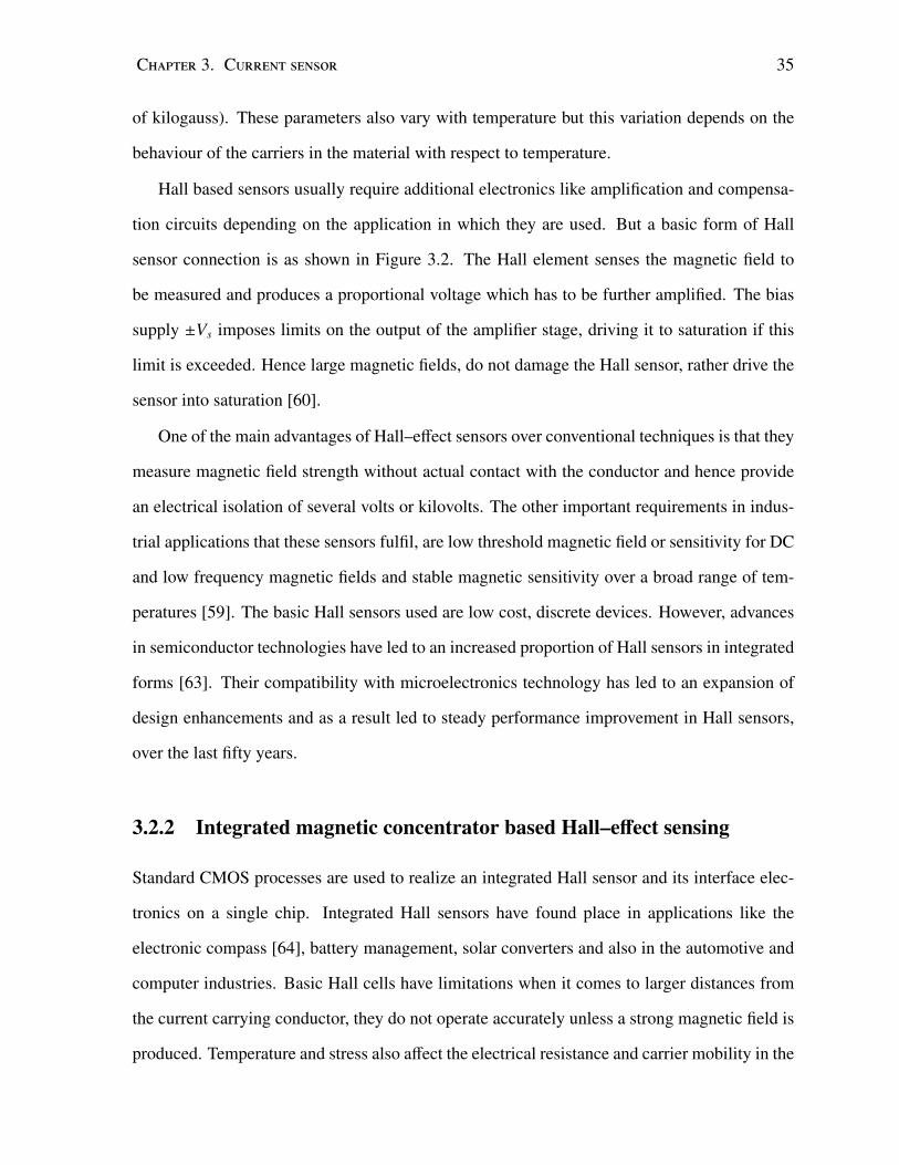
Figure 3.3: Hall–effect based sensing using Integrated Magnetic flux Concentrators.
Hall element which affect its sensitivity. Another problem is the presence of an offset voltage,
that is, the presence of a small output even in the absence of a magnetic field, due to physi-
cal inaccuracies and material non–uniformities. Integration technology allows improvement in
the sensor performance in spite of these limitations by enabling incorporation of circuits for
biasing, offset reduction, temperature compensation, signal amplification and so on [59].
One such integrated design which consists of flux concentrators in the vicinity of Hall
elements to strengthen the magnetic field seen by the element was first introduced in 1999 [65].
This configuration makes the Hall sensor suitable for measurements of even weak magnetic
fields. Such a sensor is less sensitive to external interference fields too. As in Figure 3.3,
the two flux concentrators are placed close to each other and the Hall elements are placed
below in the air gap of the concentrators. Conventional Hall ICs are made of CMOS integrated
circuits that contain lateral Hall elements at their surface. These elements by principle are only
sensitive to a magnetic field perpendicular to the chip surface. By adding Integrated Magnetic
Concentrators (IMC) made of highly permeable, low coercive field, amorphous ferromagnetic
material, directly on the chip surface, an additional field component is introduced. The two
Chapter 3. Current sensor 37
parts of the IMC collect and amplify the small magnetic flux generated around the current
carrying conductor parallel to the chip surface and locally rotate the in–plane component into a
magnetic field perpendicular to the chip surface. Therefore the Hall elements see an additional
vertical magnetic field going down on one side and going up on the other side. The sensor
output voltage is then generated by subtracting the output voltages of the two Hall elements.
This architecture of an integrated sensor can increase the flux density seen by the Hall elements
by a factor of six or more [66].
This combination of Hall–effect sensor, flux concentrator and a conductor, into a single
assembly opens up applications alternative to existing conventional current sensing methods.
This architecture decreases package size, prevents external connection of the sensor and re-
duces insertion losses [12]. The MLX sensor is one such commercially available sensor which
produces an analogue, linear, ratiometric output voltage proportional to applied magnetic field.
3.3 Summary
This chapter provides a discussion about various current sensing principles, and techniques
based on those principles that have been used in the past century and that are currently used in
commercial applications. We focus on magnetic current sensing in this chapter, more specifi-
cally on the Hall–effect based current sensing technique. Basic Hall sensing is based on Lorentz
force exerted on the current carriers within the conductor in presence of a magnetic field. A
more modern approach discussed in this chapter is the integrated magnetic concentrator based
Hall–effect sensing. We use one such commercial sensor based on the IMC principle in our
model and for our experimental measurements.
Chapter 4
Modelling and Experimental Analysis –
Piezoelectric Transformer
A fault in a power system causes changes in properties of both voltage and current signals,
for instance, resulting in an under–voltage or over–current condition. Although majority of
the faults occur due to deviation in the nature of current flow, voltage signals are preferred
for frequency estimation and fault analysis, mainly since it involves a lesser amount of risk.
This is because, during fault times, voltages can reach up to twice the maximum ratings in the
protective mechanism whereas current levels may go as high as 50 times the maximum ratings.
Consequently, there are scenarios when both voltage and current information is required for
an accurate fault analysis, for example to calculate quantities such as impedances at a point as
seen from the relay. These quantities are then compared to pre–set thresholds to estimate if the
system is operating under normal conditions. In this chapter we discuss voltage sensing using
piezoelectric transformer through actual experimental measurements and simulation results.
4.1 Finite Element Modelling and Simulation
In order to understand the piezoelectric effect and the principle of operation of a composite
piezoelectric transducer, it is necessary to analyse the piezo mathematically. Finite Element
38
Chapter 4. Modelling and Experimental Analysis – Piezoelectric Transformer 39
Modelling (FEM) of PTs is based on theory of piezoelectricity defined by mathematical equa-
tions discussed in Chapter 2. Representation of PT by the equivalent circuit method is useful
but restrictive in terms of taking into consideration effects of PT shape, size, electrode shape,
position, etc. The electrical circuit models are usually insufficient to study these PT design
aspects and their effect on PT’s performance. Hence using FEM techniques for the represen-
tation and study of PT behaviour is useful for an overall and thorough understanding of the
device properties. The other motivation for the development of model–based analysis of PT,
is the presence of different vibrational modes with very different physical characteristics. In-
corporating these characteristics completely is only possible in a 3D analysis. Optimization of
PT design by simulations without actual time–consuming experiments and ability to evaluate
new design materials without actual manufacturing are other main advantages of FEM analysis
[67].
4.1.1 Evolution of FEM analysis
A finite element analysis discussed in [67] was one of the first methods used to handle different
two–dimensional (2D) and three–dimensional (3D) piezoelectric elements for static, eigenfre-
quency, harmonic and transient analysis. 3D FEM using commercially available software like
PIEZO3D and ANS YS [68] have facilitated understanding of PT behaviour for a wide vari-
ety of electrical boundary conditions, operating frequency ranges and polarizations. A more
modernistic approach was adopted in [69] based on 3D FEM that also incorporated effect of ex-
ternal loading conditions. The electrical input admittance, output voltage and efficiency under
effect of output loading were demonstrated at resonant and half–resonant frequencies.
In a more recent study [70], owing to its simple structure and ease of fabrication, an elec-
tromechanical model for a ring type PT was presented. Based on Hamilton’s principle, a theo-
retical analysis of vibrational characteristics of piezoelectric ring was carried out in this work.
In a later work [71], a piezoelectric FEM solver employing parabolic element formulation was
developed. Rosen–modal type and unipoled–disk type PTs were studied in this work. Since
Chapter 4. Modelling and Experimental Analysis – Piezoelectric Transformer 40
Polarizations
Base Vector
Systems
Piezoelectric Devices
(.pzd)
Vin, Rload
Electrical circuit
(.cir)
Q, C
cir.Rload_v
cir.Rload_i
EigenfrequencyTime
DependentDomain
Frequency
B, displ (u,v,w)
Figure 4.1: Block diagram showing key steps involved in PT modelling with COMS OL Mul-tiphysics software and MEMS modules.
the FEM PT model has been established and improved with modifications over the years, more
recently, this concept has been extended to analyse transformers with varying cross sections
[72]. This work establishes that effects of variation of cross–sectional area of a Rosen trans-
former are significant on the location of the nodal point of operating mode, transformer ratio
and input impedance of the transformer. A more recent approach has been towards the in-
troduction of new parameters in the design of PTs; for example the introduction of alloy and
metal based electrodes [73]. Analytical method to model PT taking into account its significant
non–linearities like dielectric, piezoelectric and elastic non–linearities has been developed in
[74] based on classical piezoelectric equations.
4.1.2 Modelling using COMSOL
The PT under test is modelled as a simplified Rosen type rectangular piezoelectric transformer.
In this work, we have used COMS OL numerical solver [75] for FEM analysis of PT. The
logical diagram, Fig. 4.1, shows the modelling steps involved in modelling. The ‘Piezoelectric
Devices Interface’ within COMS OL combines mechanical and electrical characteristics for
modelling of piezoelectric devices. The displacement field and electric potential variables are
discretized by quadratic polynomials in our analysis. The ‘Piezoelectric Material Model’ is
Chapter 4. Modelling and Experimental Analysis – Piezoelectric Transformer 41
used to define the piezoelectric material properties. The mathematical equations corresponding
to our model are in stress charge form in which stress and electric displacement are expressed
in terms of strain and electric field applied. The mechanical and electrical properties of PT
are coupled using the following equations based on the fundamental piezoelectric relations
discussed in chapter 2, taking initial conditions into consideration.
(T − T0) = cE · (S − S 0) − eT · E (4.1)
(D − D0) = e · (S − S 0) + εS · E (4.2)
where, T0, S 0 and D0 are initial values assumed zero, c is elasticity and e is coupling coefficient.
The strain and electric field are defined as,
S =12· [(∇u)T + ∇u] E = −∇V (4.3)
where, u is displacement, V is electric potential. The elastic behaviour of piezoelectric media
is governed by Newton’s law and electric behaviour by Maxwell’s equation:
∇ ·T = ρ∂2u∂t2 ∇ ·D = 0 (4.4)
where, ρ is density of piezoelectric medium. Equations (4.1) to (4.4) form a complete set of
differential equations which are solved with appropriate mechanical and electrical boundary
conditions [67]. The mechanical and electrical quantities are computed for each discrete ele-
ment in the model and then solved for the entire media by interpolation. This is based on the
generalized Hamilton’s variational principle applicable to piezoelectric media which combines
differential equation of motion and charge equation of electrostatics with suitable boundary
Chapter 4. Modelling and Experimental Analysis – Piezoelectric Transformer 42
Figure 4.2: Orthogonal polarizations in input and output sections of PT.
Figure 4.3: Free tetrahedral meshing applied to COMS OL PT model.
conditions [76]:
δ
∫ t2
t1Ldt +
∫ t2
t1δWdt = 0 (4.5)
where, L is a combination of kinetic energy and potential energy available in the media or the
Lagrangian of the system, and W is the energy generated by external mechanical or electrical
excitation.
In order to verify the proposed methodologies, we created 3D model of a Rosen type PT,
which consists of input and output sections with the actual dimensions of PT used in our exper-
Chapter 4. Modelling and Experimental Analysis – Piezoelectric Transformer 43
Table 4.1: Properties of PT type C–205 used in modellingProperty Value
iments. The default polarization direction of piezoelectric material in COMS OL is along the z
axis. To associate both input and output sections of PT with orthogonal co–ordinate systems,
a new base vector co–ordinate system is introduced in the design. This method enables repre-
sentation of perpendicular polarizations in both sections with respect to each other [77], [78],
Fig. 4.2. In addition, we introduced an user defined piezoelectric material to define this model
with properties corresponding to PT under test of type C–205 [79], as shown in Table 4.1 in
the stress charge form [80]. The meshing applied is an unstructured tetrahedral mesh with size
of elements adjusted for the solution to converge with the solver employed, Fig. 4.3.
Our analysis includes three numerical experiments: 1) eigenfrequency analysis, to deter-
mine natural resonant modes of PT; 2) frequency domain analysis, to study the behaviour of
PT at various frequencies with respect to its mechanical displacement and electrical outputs;
and, 3) time dependent analysis, to observe the effects of time varying excitation on PT and
transient effects of PT.
Chapter 4. Modelling and Experimental Analysis – Piezoelectric Transformer 44
Figure 4.4: 3D plots for PT displacement (volume deformation) in nm at eigen frequencies14.79kHz, 40.71kHz, 75.62kHz, 120.57kHz, 168.05kHz and 209.04kHz
Natural Resonant Modes
For eigen analysis, the input electrodes are set to type Terminal with a nominal voltage, and
Ground conditions respectively. The output electrode is set to Floating Potential with an initial
terminal charge of zero. The 3D mechanical displacement plots, Fig. 4.4, depict a mechanical
vibration behaviour pattern for every harmonic eigen frequency. The actual resonant frequency
that corresponds to lengths and widths of PT model, results for which are reported in the
following sections, is 201kHz. We found the peak resonant behaviour in modelling to be very
close to the experimentally observed resonance of 209.04kHz. The eigen frequencies that result
from eigen analysis and cause the PT to vibrate, also have a small imaginary component that
represents a slight phase difference in the signal, caused by the propagation delay through the
PT. This is the result of the fact that signals passing through PT are susceptible to a group
Chapter 4. Modelling and Experimental Analysis – Piezoelectric Transformer 45
delay. This delay can be clearly seen in time–domain waveforms in the following explanation,
Figs. 4.12, 4.13.
When excited at harmonic frequencies, standing waves are developed and the strain dis-
tribution in the piezo changes and results in volume deformation. The harmonic eigen fre-
quencies which result in a pattern of increasing number of troughs and crests as the input fre-
quency approaches actual resonant frequency are 14.79kHz, 40.71kHz, 75.62kHz, 120.57kHz,
168.05kHz and resonant frequency 209.04kHz. Here with increase in the multiple of harmonic,
the strain distribution and hence shape of PT changes. This deformation is in the range of a
few nanometres and, as illustrated in Fig. 4.4, is scaled up and exaggerated for visual legibility.
Total displacement (nm) at 210.88kHz
10
40
70
100
Electric potential (V) at 210.88kHz
0
100
200
300
Figure 4.5: 3D plots for PT displacement in nm (top) and output potential in V (bottom) atresonance
Chapter 4. Modelling and Experimental Analysis – Piezoelectric Transformer 46
-10
-5
0
5
10
10k 105k 210k
Su
sce
pta
nce
, [m
S]
Frequency, [Hz]
Vin=1V
Figure 4.6: Simulated susceptance at the output terminal of PT model at main resonant fre-quency and at second harmonic frequency.
Frequency Domain Behaviour
For frequency domain analysis, a nominal voltage is applied to the input terminal through an
external voltage source whereas the output is terminated by a load resistance of 10MΩ. This is
done by adding the ‘Electrical Circuit Interface’. This interface introduces equations to model
electrical circuit connections coupled to the distributed field model, to solve for voltages, cur-
rents and charges associated with circuit elements. By adding this interface, a default Ground
node feature is added and is associated with node zero in the electrical circuit. The input and
output electrodes are linked to terminal type Circuit. The ‘Electrical Circuit Interface’ parame-
ters that couple model terminals to circuit elements are added accordingly. This set–up is most
useful for the ‘Time Dependent Study’.
Since the resonant frequency was found to be around 210kHz, a fine frequency resolution
simulation from 200kHz to 220kHz was carried out with an interval of 10Hz. This model being
a step–up transformer at resonance, the exact frequency at which the highest voltage transfor-
mation was recorded, was found to be 210.88kHz. We also observed maximum displacement
field and electric potential at the output electrode at this resonant frequency, Fig. 4.5.
Chapter 4. Modelling and Experimental Analysis – Piezoelectric Transformer 47
1.0
2.0
3.0
50 150 250
[V]
Frequency, [Hz]
Vin=10VVin=50VVin=75V
Vin=100VVin=125VVin=150V
-75
0
75
150
10k 105k 210k
Ou
tpu
t vo
lta
ge
, [V
]Vin=1V
Figure 4.7: Simulated frequency response of PT model showing main resonance and secondharmonic frequency (top), low frequency response (bottom) with 10MΩ load termination forvarying input voltage.
In frequency domain analysis, for a fixed input voltage magnitude, as the frequency in-
creases, susceptance of PT increases with peaks at eigen frequencies, with highest magnitude
at the resonant frequency, Fig. 4.6. Susceptance measurement in COMS OL is not inherent and
a variable B was introduced defined as the imaginary part of piezo admittance Y11. At reso-
nance, the susceptance increases to approximately 10mS. As a result of this, with increasing
frequency, potential recorded at the output edge also steps up at resonant frequency, Fig. 4.7
(top). In order to analyse low–frequency behaviour of PT model, we ran the frequency sweep
in the range of 10Hz to 250Hz. In this range, there was a step–down behaviour and a linear
increase in potential, increase in output potential was observed to be in order of few volts with
no significant peak at any frequency as was observed in the resonant frequency region. Even
Chapter 4. Modelling and Experimental Analysis – Piezoelectric Transformer 48
0
5
10
15
20
25
100 200 300 400 500 600 700 800 900 1000
Ou
tpu
t vo
lta
ge
, [V
]
Frequency, [Hz]
Rload=1MΩ
Rload=2MΩ
Rload=3MΩ
Rload=4MΩ
Rload=5MΩ
Rload=6MΩ
Rload=7MΩ
Rload=8MΩ
Rload=9MΩ
Rload=10MΩ
Figure 4.8: Simulated effect of resistive loading on PT model output behaviour in COMS OLat varying frequencies.
as the applied input voltage increases from 10V to 150V, the output voltage increases at each
frequency, Fig. 4.7 (bottom).
Behaviour of PT for varying load was also observed in the frequency domain analysis using
the ‘Electrical Circuit Interface’ and a parametric sweep with load resistance in circuit interface
as the varying parameter. For a resistive load variation of 1MΩ to 10MΩ, the PT output varies
linearly with frequency as well as with increasing load. The model response for varying load
for a frequency range of 10Hz to 1kHz is as plotted in Figure 4.8.
Time Domain Analysis
The most significant analysis carried out is the ‘Time Domain Analysis’, to test the PT model
with real–time power signals. Using this study within COMSOL it is possible to expose the
model to power–line single–tone signals as well as multi–tone faulty signals.
Chapter 4. Modelling and Experimental Analysis – Piezoelectric Transformer 49
A
B
C
G
123
45
1 - Phase to ground
2 - Phase to phase to ground
3 - Three phase to ground
4 - Phase to phase
5 - Three phase
Figure 4.9: Typical types of faults in a 3Φ power system.
In faulty conditions, the real–time simulated signal consists of a 60Hz tone intruded by
high–frequency glitches. In power systems, a fault is any aberration in a normal current flow.
In 3Φ power systems, a fault may occur either between one or more phases and ground or only
in between phases [81]. Figure 4.9 shows the typical faults in a 3Φ system.
We generated realistic time domain signals using the ‘Power System Computer Aided De-
sign’ (PS CAD) software. PS CAD/EMT DC, developed by the Manitoba HVDC Research
Centre, is an electromagnetic transient analysis program that uses a graphical user interface for
constructing input data files. This gives flexibility to work with voltage and current values out
of normal range for purpose of experimentation [82]. A power system was simulated within
this software to generate secondary voltage signals. We then performed a time domain analysis
using these exported power voltage signals applied to primary of PT model for fault type ‘phase
to phase to ground’. The ‘Interpolation’ function within COMS OL enables this generation of
input functions by exporting a data file which contains values of the voltage signals in discrete
points in time.
The primary section of PT vibrates in accord with the applied time varying input, Fig. 4.10.
At the moment when the PT encounters a high frequency glitch (here at t = 1s), its vibration
frequency also increases, and in turn increases the relative output potential generated, Fig. 4.11.
Chapter 4. Modelling and Experimental Analysis – Piezoelectric Transformer 50
-100
0
100
0 0.5 1 1.5 2
Inp
ut
to P
T,
[V]
Time, [Sec]
-100
0
100
1.0 1.2
Figure 4.10: Time–domain PS CAD generated voltage signal applied to PT model as input.
-4
-2
0
2
4
0 0.5 1 1.5 2
PT
ou
tpu
t, [
V]
Time, [Sec]
1.0 1.2
Figure 4.11: Stepped down output voltage of PT model for high voltage time–domain inputapplied
Chapter 4. Modelling and Experimental Analysis – Piezoelectric Transformer 51
-4
-3
-2
-1
0
1
2
3
4
0 0.05 0.1 0.15 0.2 0.25
Inp
ut
to P
T,
[V]
Time, [Sec]
Scaled input to PTPT model output
Figure 4.12: Simulated phase delay between input to PT model and output recorded for thatinput for 60Hz component.
Although the high voltage sinusoidal input is stepped down by the PT, the high frequency
components in this input are amplified relative to the 60Hz components of this input.
4.1.3 Other considerations
Group delay
Group delay is a measure of time delay of amplitude envelopes of various sinusoidal compo-
nents of a signal through a device under test, PT in our case, and is a function of frequency of
each component. When a signal composed of multiple frequency components passes through
PT, it suffers distortion because these components are not delayed by the same amount of time
at the output of the PT. This changes the shape of the signal in addition to any constant delay
or scale change [83]. In COMS OL, during the ‘Time Dependent Study’, we observed that low
frequency signals exhibit longer lags after passing through PT while, in comparison, higher
Chapter 4. Modelling and Experimental Analysis – Piezoelectric Transformer 52
-4
-2
0
2
4
6
0.996 0.998 1 1.002 1.004 1.006 1.008 1.01
Inp
ut
to P
T,
[V]
Time, [Sec]
Scaled input to PTPT model output
Figure 4.13: Simulated phase delay between input to PT model and output recorded for thatinput for high frequency component.
frequency tones exhibit progressively shorter delays. We found this delay to be less than 3ms
consistently for the 60Hz component, Fig. 4.12. This delay was negligible for high frequency
components and the signal appeared at PT output almost at the same time as it was applied to
PT’s input, Fig. 4.13.
Propagation velocity, PT dimension and resonant frequency
Another property demonstrated in our model is the dependence of the PT resonant frequency
on its physical dimensions. The velocity of propagation ν through piezoelectric ceramic also
depends on its vibration mode. For a particular shape and vibration mode, the wavelength of
vibration λ is related to its propagation length l at a resonant point by,
λ
2= l (4.6)
Chapter 4. Modelling and Experimental Analysis – Piezoelectric Transformer 53
Table 4.2: Effect of length of PT (l) on resonant frequency ( fR) and on low frequency outputvoltage
Although a PT proves to be a good isolation transformer as compared to conventional
electromagnetic transformers, when used in power systems, occasional sudden surges may
cause damage if propagated from input to the output. Isolation of high power input side from
low power control circuitry is important for prevention of damage due to these sudden surges in
power systems. One way to achieve ground decoupling, is to connect two PTs in a differential
configuration [87], Fig. 4.15. Another method to deal with these spurious high frequency
surges is to use excessive filtering and signal processing at the input of transformer. One such
efficient actuating circuit, small in size but with a wide input voltage range is developed in [88].
Chapter 4. Modelling and Experimental Analysis – Piezoelectric Transformer 56
PSCAD running on computer RTP playing back real-time waveforms
Adapter
Omicron amplifier
LoadPT
Vin
Vout
Oscilloscope
Network
Figure 4.16: Experimental set–up for measurements with real–time input signals.
4.2.2 Experimental requirements and set–up
The equipment used for single–tone and real–time measurements, both at resonant frequency
and low frequency region are:
1. The Agilent 33522A Function/Arbitrary Generator as the single–tone input voltage source;
2. Tegam Model 2350 Dual Channel High Voltage Precision Power Amplifier used as a
voltage amplifier for higher inputs to PT;
3. PC running PS CAD software to generate realistic power voltage signals;
4. Real Time Playback (RT P) Simulator to playback the real–time signals generated by
PS CAD;
5. OMICRON CMS 156 three–phase voltage and current amplifier;
Chapter 4. Modelling and Experimental Analysis – Piezoelectric Transformer 57
6. Tektronix DMM4040 6.5 Digit Precision Multimeter for metering and recording the out-
put;
7. Tektronix DPO7354C Digital Phosphor Oscilloscope for output signal monitoring and
measurements.
Figure 4.17: Most recent experimental set–up for measurements with real–time input signals.
To test the PT with realistic power signals, like in the simulations, we used the PS CAD
software to generate real–time fault–free and faulty signals. PS CAD on a computer interface
is used in combination with an RT P simulator to physically recreate these signals. The RT P
suite of tools is a computer based testing environment useful for testing power systems. It is
an analogue/digital arbitrary waveform generator, specifically designed to harness the power
of PS CAD simulation software. The PLAYBACK program within RT P allows display, con-
figuration and complete control of the waveforms to be played back [89, 90]. Since the RT P
simulator has a voltage limit for playback, these waveforms are then amplified by use of the
Chapter 4. Modelling and Experimental Analysis – Piezoelectric Transformer 58
OMICRON amplifier to the level of actual secondary voltage signals before being applied to
PT input terminal. This complete set–up is shown in Figure 4.16.
The later part of experiments were done using a new set–up, Fig. 4.17, for which a combi-
nation of the arbitrary function of the signal generator and the high–voltage amplifier was used
to generate input signals applied to the PT.
4.2.3 Single–tone results
0.2
0.6
1.0
50 150 250
[V]
Frequency, [Hz]
Vin=10VVin=75V
Vin=150V
0.1
0.5
2.0
10.0
10k 100k 200k
Outp
ut voltage, [V
]
Vin=1V
Figure 4.18: Experimentally recorded frequency response showing main resonance and secondharmonic frequency (top), low frequency response (bottom) with no load condition for varyinginput voltage.
Results for the 201.4kHz resonant frequency PT are presented and discussed in this section.
Chapter 4. Modelling and Experimental Analysis – Piezoelectric Transformer 59
For an AC input signal of amplitude 1Vrms and near the PT’s fundamental resonance, in its
single–ended mode, it behaves as a step–up transformer with peak responses of about 20V
and 2V respectively at resonant and half–resonant frequencies, Fig. 4.18 (top). However at
lower input signal frequencies, ranging from 10Hz to 250Hz, the transformer steps down input
voltage as high as 150V, Fig. 4.18 (bottom). For an input ranging from 10V to 150V, we found
that the output voltage increases linearly with no significant peak at any frequency, Fig. 4.18
(bottom).
-10
-1
2
50 100 150 200 250
Err
or
[%]
Frequency, [Hz]
0.2
0.4
0.6
Outp
ut voltage, [V
] ExperimentalFitted data
Figure 4.19: Experimentally recorded low frequency response for 100Vrms input overlappedwith results of the fitting linear function of the form y = ax + b (top), percentage error betweenmeasured output and fitted data (bottom).
We therefore found this step–down behaviour of PT in low frequency region to be linear
Chapter 4. Modelling and Experimental Analysis – Piezoelectric Transformer 60
with respect to both frequency and the applied input voltage. To demonstrate this, for an
input of 100V to the PT, the output voltages measured from 10Hz to 250Hz signal frequency
are mapped into a linear function of frequency. Using a simple curve fitting tool, this linear
relation between input frequency and output voltage was found to be y = 0.0029x + 0.0065,
which closely represents the recorded output voltages, Fig. 4.19 (top). The error percentages
calculated between actual recorded output voltages and linearly fitted outputs lie within ±1%
for the frequency range of interest. Similarly, the output voltages measured were also found
to be linearly varying with respect to applied input voltages. This PT action was observed
consistently up to approximately 2kHz. This property of consistent linear behaviour of PT
in power–line frequency region makes it useful in low power consumption area of voltage
transformation in power systems.
4.2.4 Loading Effect
0
1
2
3
4
5
6
50 100 150 200 250
Ou
tpu
t vo
lta
ge
, [V
]
Frequency, [Hz]
Vin=100V (BNC)Vin=100V (Passive probe)
Figure 4.20: Experimentally recorded low frequency response for 100Vrms input using a regularBNC compared with passive probe demonstrating loading effect.
Chapter 4. Modelling and Experimental Analysis – Piezoelectric Transformer 61
0
0.5
1
1.5
2
100 200 300 400 500 600 700 800 900 1000
Ou
tpu
t vo
lta
ge
, [V
]
Frequency, [Hz]
Rload=0.98MΩ
Figure 4.21: Experimentally recorded effect of resistive loading on PT output behaviour forvarying frequency
As seen in the set–up, the PT output is connected directly to the oscilloscope using BNC.
This causes the oscilloscope to load the PT circuit, since the input impedance of the scope
becomes significant and affects the actual measurement. The oscilloscope used in the set–up
has analogue channels that introduce 1MΩ, 13pF input impedance. The output impedance of
PT in the low frequency region is high. With a normal BNC connection, the scope impedance
becomes considerable in drawing signal current from signal source and hence attenuates the
actual measured PT device output signal. To maintain maximum output signal fidelity, we used
a frequency compensated passive (10X) probe, with a 10MΩ, 8pF impedance to compensate
for the input impedance of the scope. With this probe, the output is almost exactly equal to
the actual PT output that should be, without any loading effects. The amplitudes are higher
as compared to those measured using normal BNC with a relatively higher slope linearity.
An example with 100Vrms input is as seen in Figure 4.20 where the output voltages vary in
amplitude when measured using the passive probe.
The current which contributes to mechanical vibration in piezo material, depends on load
resistance. Hence resonant and higher harmonic voltages are functions of load resistance and
Chapter 4. Modelling and Experimental Analysis – Piezoelectric Transformer 62
the effects are examined in [91]. Loading affects quality factor and the PT electrical impedance
and hence affects resonant behaviour of PT. The PT’s output static capacitance is characteristic
of its output impedance. In the resonant frequency region, when load impedance becomes com-
parable to output impedance of PT, it sinks more mechanical power and the step–down/step–up
ratio begins to drop [32]. This drop can be understood by considering the fact that the static
output capacitance and the load impedance form a high pass filter. The real part of this high
pass filter deviates the resonant frequency, while its imaginary part reduces the quality factor.
PT voltage gain, power and efficiency are therefore load dependent; voltage gain increases with
the load and reaches a maximum in open circuit condition (infinite load) [85]. A similar be-
haviour is observed in the low frequency region. Characterization of the PT with loads ranging
from 1kΩ to 1MΩ yields a linear trend in output voltages.
Due to the practical limitations of low frequency measurements in our current set–up,
highly accurate frequency response for variation in load impedance is difficult to obtain. Fig-
ure 4.21 shows PT response for an external resistive load of 0.98MΩ at PT’s output, for fre-
quency variation in the range 10Hz to 1kHz. At 60Hz, the output is approximately 0.155V
for 0.98MΩ load, with an evaluated current value of 0.16µA which gives an approximate VA
rating of 0.0245µVA. It should be noted that these secondary signals obtained at piezo output
only serve as the input signals to an ADC and/or other integrated circuits (ICs), and hence these
low power signal levels are preferred.
4.2.5 Real–time analysis
The next set of results were obtained for realistic power system signals. An earlier work in-
vestigates time–domain characteristics of transient response of PT with open–circuit operation
[92]. The results in this work are however obtained when a high voltage transient is induced at
the input terminals of PT immediately after an AC voltage connected to the PT is switched off.
Very little research has been done in the area of time–domain and transient response of PTs.
In our work, in order to analyse PT behaviour with real–time signals, we have considered
Chapter 4. Modelling and Experimental Analysis – Piezoelectric Transformer 63
Figure 4.22: Schematic diagram for PS CAD case 1 power system simulation model example.
Figure 4.23: Schematic diagram for PS CAD case 2 power system simulation model example.
two cases in PS CAD that simulate two 3Φ substations connected via a single transmission
line. The in–built power system model consists of two impedance sources connected via a
100km transmission line. It has a settable system voltage via source equivalents and full fault
control panel with various fault combinations for different positions and types. A snapshot of
the models used in PS CAD are demonstrated in Figures 4.22 and 4.23. In case 1, a fault occurs
between source 1 and circuit breaker 1. In the case 2, a fault occurs at midpoint between two
segments of transmission line T1 and T2. In both cases, we evaluated faults both between
any two phases, and between phases and ground. These signals were recreated using the RT P
simulator and applied to PT through the high–power amplifier. A fault–free power–line voltage
signal contains only a pure 60Hz tone. But a faulty signal is intruded with higher frequency
and glitches of varying amplitude.
The PT output demonstrated here is for case 2 and the fault type considered is the AB-g
fault. The total duration of the signal applied to PT was 5s. The fault was controlled to occur
at 2s and last for a duration of 0.5s using the timed fault logic within the power system model.
Chapter 4. Modelling and Experimental Analysis – Piezoelectric Transformer 64
-0.3
-0.2
-0.1
0
0.1
0.2
0.3
0.4
1.8 1.9 2 2.1 2.2 2.3 2.4 2.5 2.6 2.7
PT
ou
tpu
t, [
V]
Time, [Sec]
Measured PT output
Figure 4.24: Stepped down PT output voltage for high power input applied experimentally
The breaker in this model, controlled by a timed breaker logic, is not used in our case since we
want to apply the actual secondary fault voltage to PT, before any fault corrective action. For
this applied input, the PT output is a stepped down sinusoidal output voltage. Here, similar to
as observed in the model behaviour, although the high voltage sinusoidal input is stepped down,
high frequency glitches are amplified relative to the 60Hz component, Fig. 4.24. The amplitude
of these glitches is usually 10− 20% of amplitude of power–line frequency component. Hence
although these high frequency glitches are amplified to more than 10−20% of the stepped down
output voltage, they still get attenuated. The same experimental set–up as in the single–tone
measurement is used to record this output.
4.2.6 Experimental group delay measurement
In power systems, power line frequency sometimes is intruded by unwanted spurious high
frequency transients, which if propagated may result in damage of the system. Usually high–
Chapter 4. Modelling and Experimental Analysis – Piezoelectric Transformer 65
0
1
2
3
4
5
6
50 100 200 500 1000
Gro
up d
ela
y, [m
s]
Frequency, [Hz]
Figure 4.25: Experimentally measured group delay through PT sample for varying frequencies.
speed protective relays are used to detect faults which occur as a result of these noise frequen-
cies which deviate in phase and magnitude with respect to power–line frequency. These noise
frequencies vary from hundreds of Hz to a few kHz. The relays make a decision about the
severity and location of fault based on the properties of the signal; such as phase, magnitude of
voltage or current signals, impedance etc. The faster a fault is detected, lesser time it takes for
the signal to restore its fault–free steady state [93].
Signals passing through PT are susceptible to group delay as discussed in the previous
section. Measured group delay pattern for frequency range 40Hz to 1kHz shows an expo-
nential decay, Fig. 4.25. For 60Hz signal, delay is approximately 5ms, which progressively
decreases to less than 1ms for frequencies above 200Hz. Eventually, as we increase the tran-
sient frequency beyond 1kHz, the delay time reduces to few microseconds. This behaviour
of the transformer enables fast and accurate detection of disturbances while operating at line
frequency.
In our time domain simulations, we subjected the PT model to low frequency and high
frequency signals, to demonstrate this lag. This delay was likewise observed when PT was
treated with the real–time PS CAD signals just as shown for the simulated PT model. For a
5s long input with high frequency glitch occurrence at 2s, Figure 4.26 shows a noticeable lag
between the scaled down input to PT and the PT output in the low frequency component. This
Chapter 4. Modelling and Experimental Analysis – Piezoelectric Transformer 66
-0.3
-0.2
-0.1
0
0.1
0.2
0.3
0.4
1.96 1.97 1.98 1.99 2 2.01 2.02 2.03
[V]
Time, [Sec]
Input to PT (Scaled)PT output
Figure 4.26: Experimentally observed group delay through PT sample for real–time faultyinput signal.
lag is negligible when the PT encounters a high frequency glitch at 2s. Hence the glitch appears
almost at the same time at the output terminal as it appears at PT’s input terminal, making it
instantaneously detectable.
4.3 Limitations of PT considering existing system conditions
The electrical equivalents and mathematical models established for PT are based on its opera-
tion at or near its resonant frequency. In our experimental work we noticed the following three
important practical limitations related to PT operation that we need to keep in mind, since we
use the PT in low frequency area of operation.
• Mechanical considerations
• Non–linearity and Hysteresis
Chapter 4. Modelling and Experimental Analysis – Piezoelectric Transformer 67
• Material properties, ageing and effect of temperature
4.3.1 Mechanical considerations
A PT operates based on the principle of energy transfer through vibration. The vibrations in
input and output sections may not necessarily follow the same patterns. Mechanical vibration
has a non–uniform distribution over the dimension of PT [94]. The vibration pattern in the PT
not only depends on factors like the frequency of operation and terminal load impedance but
also on the structural constraints and device clamping that the PT might have been exposed to.
We have observed noticeable differences in the PT performance when mounted on a test–bench
table top and when held firmly onto a printed circuit board with a cable tie, Fig. 4.27.
Figure 4.27: Photo of a PT size compared to a Canadian penny, held using cellophane tape(left), PT clamped on to a PCB using a cable tie (right).
Hence it is important to design an appropriate package and make electrical connections
to PT without affecting its operation and efficiency. Having said that, considering one of the
reasons of using a PT is lesser space occupancy, since its size is small as compared to a con-
ventional board based electromagnetic transformer, Fig. 4.27, care must be taken to confine the
size of the package used. There have been inventions related to PT device being packaged in
moulded cases with conductive adhesive for external electrical connections, use of conductive
sheets and spring terminals, latched upper and lower cases for piezo body etc. One improved
armoured case has been discussed in [95], which comprises of a moulded package with re-
duced thickness and with projections to mechanically support the piezoelectric element. The
Chapter 4. Modelling and Experimental Analysis – Piezoelectric Transformer 68
thickness reduced moulded package with projections is capable of applying an elastic force on
the piezo element such that the element is confined within the package walls but still separated
from them. These projections also provide an avenue for wirings to make electrical contact
with the element.
Another method discussed in [96] suggests a mechanically compliant apparatus which re-
lates to mounting PT onto a PCB with use of miniature conductive springs. It describes a
configuration for Rosen–type PT operating in one–lambda length resonance mode as an exam-
ple, with coil springs attached to at least one minimum displacement node of PT, to minimize
mechanical stress on it. The output electrical connection is made at the maximum displacement
point which is extremely sensitive to mechanical dampening.
A later invention [97], describes an integral construction of the housing and the lead frames
for the PT which enables easy contact with PT and resilient support to PT at the same time.
This design is suitable as an alternative to the simple PCB design with soldered wires that we
used in our experiments, especially for mass production to avoid repetitive wire connections
and breakage of wire contacts at solder points. The housing consists of an upper and lower
section with a protrusion to support PT, and lead frames made of conductive elastic material to
be in contact with PT electrodes. These sections couple with each other with a hook and snap
arrangement.
Designing a system taking into account all these factors will be a significant step towards
integration of sensing devices. Since we only harness the low frequency properties of PT, we
need not take into consideration the wavelength vibration modes while designing a clamping
structure. Nevertheless, the sensitivity of PT with respect to mechanical vibration is higher in
the low frequency region, which is our area of application and hence a resilient housing that
resists external unwanted vibrations, which affect the PT performance, is essential.
Chapter 4. Modelling and Experimental Analysis – Piezoelectric Transformer 69
0
0.5
1
1.5
2
20 40 60 80 100 120 140
Ou
tpu
t vo
lta
ge
, [V
]
Input voltage, [V]
Low to high input transitionHigh to low input transition
Figure 4.28: Negligible hysteresis observed during experimental measurements at power–linefrequency.
4.3.2 Non–linearity and Hysteresis
Piezo material is inherently non–linear mainly due to the domain orientations in the piezo mate-
rials which cause the dielectric non–linearities. The piezoelectric non–linearities are attributed
to the dependence of piezoelectric constants on polarizations, electric field components and
mechanical pressure. The elastic non–linearities originate from the fact that excessive me-
chanical stress on PT may cause depolarization of its material and may alter its dielectric and
piezoelectric properties [74]. In low frequency mode, we demonstrate the PT linear behaviour
and hence incorporating a correction factor for non–linearity is not required. However, in the
higher frequency and high input voltage region, hysteresis at the PT output becomes visible.
Hysteresis is a common phenomenon in smart actuators like piezoelectric transducers,
which may act as an additive disruption in the dynamics of the device. The effect of hysteresis
is considered to be a combination of both amplitude and phase distortion [98]. We observed
a hysteresis specifically with respect to PT output magnitudes for input variation from low to
high voltage and from high to low voltage. Although the difference in magnitudes is almost
negligible, Fig. 4.28, it could be measurable at high frequencies. We partially eliminated this
Chapter 4. Modelling and Experimental Analysis – Piezoelectric Transformer 70
Figure 4.29: Photo of PT with mechanical defect.
effect by using two PTs in a differential configuration.
4.3.3 Material properties, ageing and effect of temperature
The PT’s performance is fundamentally limited by the material itself, by its mechanical strength
and depolarization due to heating and constant exposure to stress and strain [33]. The mate-
rial’s thermal limitations and maximum capacity to withstand stress and strain may limit the
PT functionalities. During the energy transformation process between primary and secondary
sections of the PT, the PT undergoes mechanical and electrical losses that generate heat within
the device. The equivalent PT losses are proportional to the quantity of heat produced in the
PT body. The PT can dissipate some amount of heat produced in its body which reduces the
increase in temperature. This ability of heat radiation is proportional to PT’s ratio of surface
area to volume. This makes the rectangular cross section more efficient with respect to heat
dissipation than a circular cross section for a PT.
Due to low thermal conductivity of PT material, constant exposure to high voltages may
cause overheating of the material which eventually leads to depolarization effects if the temper-
ature inside the PT exceeds a critical level. This critical temperature determines the operational
limit as the PT must be operated below the Curie Temperature (TC) to prevent permanent dam-
age to the device. This temperature limit is typically between 150C to 250C for most PZT
ceramics, at which point domain rotation begins, long before the actual TC of about 300C,
Chapter 4. Modelling and Experimental Analysis – Piezoelectric Transformer 71
due to the combined effect of high temperature and electric field [99]. Typically at resonance,
the piezo operating parameters remain almost constant in the −40 to +150C range. Since
we are operating at low frequencies, this range will almost never be exceeded but cannot be
ruled out in case of faulty signals that cause power–line frequency signal to be intruded by
high frequency transients. Practically, this can be confirmed only with use of devices like the
thermographic cameras.
Temperature change may also lead to thermal stress, which causes the shift of the optimum
operating point for the PT even below the threshold for mechanical failure and TC, making
it sensitive to the slightest change in operating conditions [77]. Exposing our experimental
PT to high voltages constantly especially near resonance, made it mechanically sensitive near
the junction of input and output sections and caused it to break into two with just a single
tap, Fig. 4.29. This was one case of mechanical defect observed during our experiments.
Although the exact cause of this breakage could not be established conclusively, since the
PT broke exactly at the centre, the reason can be attributed to degraded sensitivity at the point
of maximum stress within the piezo.
Device degradation due to natural time evolution, called ageing, which causes a drastic
decline in the functional performance of the material with time, is another factor we have to
take into consideration. This is caused by the constant realignments of domains within the
material to form more stable configurations [100]. Hence, it is important to quantify variations
in performance of a PT in the application field over longer periods of time.
4.4 Summary
Evolution of FEM techniques used for PT design has led to experimentation with varied struc-
tures without actual manufacture processes. We discuss one such simple model in COMS OL
in this chapter, which incorporates both electrical and mechanical properties. We recorded
simulation results using this model for eigenfrequency analysis, frequency response of the PT
Chapter 4. Modelling and Experimental Analysis – Piezoelectric Transformer 72
for different applied inputs and time–based PT responses. Based on these preliminary studies,
we demonstrate the effects of PT dimension, material, frequency of operation and amplitude of
stimulating voltage input on its electrical output.
Following the simulation results, we present an experimental analysis in this chapter. Rosen–
type piezo ceramic transformers from ‘Fuji Ceramics’, with different dimensions and made to
resonate at different frequencies, were used for experimental purposes. All the devices, instru-
ments and methods used for actual PT measurements are illustrated in this section. The two
connection types used, single–ended and differential, are discussed along with their character-
istics.
In order to test the PT with real–time faulty signals, it is important to have an elementary
understanding about types of faults. We discuss faults specific to 3Φ power systems to iden-
tify nature of these faults. Single tone PT measurements with predefined signal frequency and
amplitude are recorded. Response of the PT to varying signal frequency with a constant am-
plitude both in power–line frequency region and near resonance is observed. These responses
were found to be in agreement with the simulated results. The PT behaviour in the low fre-
quency region can be mapped into a linear relation between input frequency and output voltage.
Similarly, for a fixed signal frequency, the PT outputs for a varying signal amplitude were noted
to observe effect of high voltages on the PT.
Being a high output impedance device at low frequencies, it was concluded that the PT
does not yield accurate results without an impedance matching network or an intermediate
buffer circuit between the PT and loading circuit. The loading effect deteriorates the PT’s
resonant as well as low frequency behaviour. With corrective measures, the effect of externally
connected load values on the PT output was observed and plotted.
To be able to use PT seamlessly as an alternative to existing magnetic sensing technique,
it is necessary to test it with real–time power signals. This real–time analysis with actual
power system signals, was possible with use of signal generators in combination with power
simulation software programs like PS CAD and PLAYBACK. Effect of time varying voltage
Chapter 4. Modelling and Experimental Analysis – Piezoelectric Transformer 73
signals for the considered cases during normal and faulty conditions was recorded. The group
delay measurements led to the idea of fast detection of high frequency glitches using PT while
stepping them down.
Finally, certain drawbacks associated with using PT in our application are brought out in
this chapter. Although the analytical and experimental results indicate promising future for
piezo devices in power applications, effect of factors like external mechanical perturbations,
temperature variations and material degradations pose some significant challenges in adopting
these transformers. With suitable mounting designs and device manufacturing, taking into
account the application environment, it is possible to employ PTs in high power systems.
Chapter 5
Modelling and Experimental Analysis –
Hall sensor
Current sensing and measurement is required in relay systems to calculate quantities such as
impedances. Current signals are also used for frequency estimation for protection and control
functions performed by the relay. During 3Φ solid faults, when all three phases are shorted
to ground with zero impedance, pre–fault voltage values in combination with current values
recorded at that time, help in fault diagnosis.
In power systems, large line currents in order of kA are scaled down to few amperes, by cur-
rent transformers (CT). During normal operation, secondary rating of connected CT is matched
to relay’s nominal input current resulting in a stepped down value of 1A or 5A. This is mostly
done by use of auxiliary electromagnetic transformers. Conventionally, this current is then con-
verted to a voltage with use of sense resistors and further digitized for measurement purposes.
The sensor chosen in this work as an alternative to resistive sensing for testing and analysis is
Hall based MLX91205 integrated magnetic sensor. Whenever a fault occurs, changes in fre-
quency and amplitude of voltage signals are accompanied by a spike in current signals. There-
fore, the current signal corresponding to a fault condition simulated in PS CAD was recorded
and treated with current sensor.
74
Chapter 5. Modelling and Experimental Analysis – Hall sensor 75
Vout
IinIout
MLX IC
Figure 5.1: Photo of development kit used for measurements based on IMC MLX91205 IC andits 3D rendering showing narrow conductor width under the IC
5.1 Device under test
We experimented with the low field MLX91205 IMC sensor for our application. The IMC
91205 Hall sensor is fabricated with conventional CMOS technology with an additional fer-
romagnetic layer. This IMC layer is used as a magnetic flux concentrator which provides a
magnetic gain of about 3 to 6, to increase the output signal without an increase in the inherent
sensor electrical noise. The MLX91205 is a SOIC8 packaged device suitable for surface mount
PCB construction and miniaturization. In this structure, the measured current is passed either
directly through a current track of the PCB located under the sensor, or the sensor is mounted
at a given distance from a larger current conductor like a busbar. It is a simple device and pro-
vides an analogue output voltage proportional to the magnetic field generated by this current
carrying path [101].
The set–up used in our experimental measurements is a development kit from Melexis
[102], Fig. 5.1. It includes the IC mounted on a PCB with signal tracks for current measure-
ment. It has slots on either sides of the IC to insert an U–shaped magnetic shield to concentrate
the magnetic flux density seen by the IC. This sensor is sensitive and linear in the frequency
band of DC to 100kHz, and has a response time of 8µs. It has an operating range from −40C
to 125C and requires a DC power supply of 5V. It is possible to increase the magnetic field
Chapter 5. Modelling and Experimental Analysis – Hall sensor 76
Figure 5.2: 3D COMS OL model representing the Hall–effect based IMC concept showing theconductor with lateral Hall elements and two hexagonal magnetic concentrators.
density with the same current magnitude by narrowing part of conductor that passes right below
the chip surface. This action increases the current density in the narrow portion underneath the
IC and generates higher magnetic flux density around it, thus it increases the field magnitude
as seen by concentrators. The IMC sensor makes use of this concept, and therefore further
increases the sensitivity of the sensor.
This device, along with the Hall elements, also incorporates offset cancellation circuitry,
current source, chopper stabilized amplification circuitry and parameter programming capa-
bility [103]. The inherent drawbacks of IMC technology related to process and material are
overcome by an appropriate sensor architecture which varies with the requirements of the ap-
plication [104] making it a highly accurate technology. Along with the actual measurements
using this IC, we also modelled the IMC principle in COMS OL. Using the model we demon-
strate the effects of current magnitudes, direction and dimension of the device on the output
result.
5.2 COMS OL model and effect of real–time PS CAD current
signals
We use a Copper conductor in the model to represent the current carrying path with Hall ele-
ments and two hexagonal highly permeable structures (we used Iron from the in–built Materials
Chapter 5. Modelling and Experimental Analysis – Hall sensor 77
Normal magnetic flux density (T)
Figure 5.3: Simulated effect of varying width of the part of the conductor under the Hallelements, on normal magnetic flux density distribution in the COMS OL model.
library in COMS OL) to represent the concentrators, Fig. 5.2. This assembly is modelled to be
placed in an air surrounding. The ‘Magnetic Fields’ (mf) physics module was used for the
simulations. Effect of 5A current through the conductor was first observed in terms of flux
distribution in the assembly.
The effect of current flow through the conductor path under the IC and dimension of this
conducting path has an effect on the magnetic field seen by the Hall elements within this IC.
As mentioned in the previous section, the IMC sensor makes use of this principle to increase
its sensitivity to low fields. We demonstrate this effect by varying the width of the part of
conductor which lies below the concentrators and Hall elements in our COMS OL model using
a parametric sweep function and 3D plots. Although the output recorded is not in form of
Chapter 5. Modelling and Experimental Analysis – Hall sensor 78
an output potential, the magnetic fields observed in the model are evidence to this effect. For
the same current passing through the conductor, the normal magnetic flux density observed in
the narrow region between the concentrators around the conductor increases with decrease in
width of that conductor in this narrow region, Fig. 5.3. Increase in the width also increases
power dissipation and self–heating of the conductor.
-40
-20
0
20
40
0 0.1 0.2 0.3 0.4 0.5
Ma
gn
etic f
lux d
en
sity,
z c
om
po
ne
nt,
[T
]
Time, [sec]
x10-12
Right edgeLeft edge
Figure 5.4: Simulated z component of magnetic flux density variation observed between thehexagonal concentrators along the two facing boundaries in the model.
Since the material used for the concentrators in the IMCs and in our model has a high
permeability, the concentrator collects all the flux lines in its vicinity and focuses them on the
Hall elements. Along with the flux around the conductor due to the current it carries, we also
observe flux lines parallel to the conductor. The concentrators make part of these flux lines
pass through the Hall elements underneath, as for these elements, flux appears to be going up
on one side of the concentrator and going down on the other side of the concentrator. For a
current of 5A through the conductor in our model, we observed the perpendicular component
Chapter 5. Modelling and Experimental Analysis – Hall sensor 79
of this magnetic field to be strongest near the gap between the concentrators. The flux recorded
along both sides of the concentrators facing each other in the gap was opposite in polarity to
each other, Fig. 5.4, which indicates that flux lines travel up on one side and down on the other
side. In actual implementation, this field gives rise to a potential difference in the gap and
hence a difference in magnetic field seen by two Hall elements. The sensor output voltage is
now generated by difference in output voltages produced by these two Hall elements.
-6
-4
-2
0
2
4
6
8
10
0 0.1 0.2 0.3 0.4 0.5
IAse
c,
[A]
Time, [sec]
No faultFault at t=0.2s
Figure 5.5: Time–domain plot of secondary current exported from PS CAD power systemmodel applied to Hall model in COMS OL, for fault and no fault condition.
The sensor’s upper limit for measurable current level is determined only by the physical
construction of the device, since the output voltage is dependent on conductor size and its
distance from sensor. This is a useful property in our application since, during fault conditions,
continuous current levels may easily go up more than three times the normal levels. Lower
currents up to ±2A can also be measured by increasing magnetic field via a coil around the
sensor. The sensitivity is further increased by adding a shield around the coil and sensor set–
up.
We observed the dependence of time varying current signal passing through the narrow
Chapter 5. Modelling and Experimental Analysis – Hall sensor 80
-10
-5
0
5
10
0 0.1 0.2 0.3 0.4 0.5
Ma
gn
etic f
lux d
en
sity,
z c
om
po
ne
nt,
[T
]
Time, [sec]
x10-12
Right boundaryLeft boundary
Figure 5.6: Time–domain plot of z component of magnetic flux density recorded on concentra-tor boundaries facing each other in the gap, for time varying input current.
conductor upon magnetic field density around the conductor in our model. Figure 5.5 shows
the applied current input exported from PS CAD corresponding to case 2 AB-g fault condition
compared with a no–fault condition current. The faulty signal shows fault occurrence time as
0.2s and duration of fault as 0.2s. During this time, magnitude of current rises more than four
times as compared to no–fault current signal. We use ‘Time Dependent’ study in COMS OL to
probe the gap boundaries of concentrators to observe magnetic field distribution. The perpen-
dicular components of magnetic field recorded on the boundaries of concentrators facing the
gap in which Hall elements are placed, follow a similar sinusoidal trend as that of current, and
varies from minimum −5pT to maximum of approximately 13pT, Fig. 5.6. During the fault,
magnetic field increases more than five times as compared to the normal fault–free conditions.
The flux density on each of the faces is opposite in polarity to each other.
In the actual IMC circuit, this magnetic field is seen by Hall elements within the IC and
corresponding output voltage is generated. Due to the increase in strength of magnetic field
during fault times, an analogous potential which indicates presence of fault is generated. Based
Chapter 5. Modelling and Experimental Analysis – Hall sensor 81
Bias100nF
&
Supply
+5V
Out1
Out2
MLX91205
1nF 1nF
Vout
Figure 5.7: Schematic diagram of direct single–ended connection for the open loop MLXcurrent sensor.
on the characteristics of this Melexis sensor and the output potential, the actual current values
will be estimated in power system applications.
Due to experimental limitation, we could not test the actual IC with real–time PS CAD
produced signals. However, we tested the MLX91205 sensor in its open loop configuration for
a single–ended direct output with bypass capacitors connected for a reliable operation, Fig. 5.7.
Our measurements with the MLX device for constant current inputs resulted in a set of plots
that show effect of change in current amplitude and frequency on output voltage. We compared
these results with the magnetic field trend observed in the COMS OL model. Figure 5.8 (top)
shows increase in normalized output voltage with increase in current input for the MLX sensor.
The magnetic field (z component) in COMS OL simulation follows a similar trend with increase
in current. When tested for increasing frequency and for a constant current input of 1A and
5A, Fig. 5.8 (bottom), change in output voltage was relatively constant with a decrease of about
5mV for the MLX sensor. COMS OL plot of corresponding magnetic field shows a decreasing
trend too with much lower magnitudes and a different scale of measurement.
Chapter 5. Modelling and Experimental Analysis – Hall sensor 82
30
60
90
120
150
0.5 1 1.5 2 2.5 3 3.5 4 4.5 5
3
9
15
Ou
tpu
t vo
lta
ge
, [m
V]
Ma
gn
etic f
lux d
en
sity,
z,
[T]
Current, [A]
x10-13
Output voltageMagnetic flux density (right boundary)
0.05
0.1
0.15
0.2
0.25
100 200 300 400 500 600 700 800 900 1000
5
10
15
20
25
Ou
tpu
t vo
lta
ge
, [V
]
Ma
gn
etic f
lux d
en
sity,
z,
[T]
Frequency, [Hz]
x10-13
Output voltage for 1AMagnetic flux density (right boundary) for 1A
Output voltage for 5AMagnetic flux density (right boundary) for 5A
Figure 5.8: Experimentally recorded MLX output voltage for increasing current, flux variationwith current in COMS OL model representation (top), Experimental MLX frequency response,recorded flux change with frequency in COMS OL Hall model representation, for 1A and 5A(bottom).
Chapter 5. Modelling and Experimental Analysis – Hall sensor 83
5.3 Other considerations in IMC based Hall sensing
Techniques like narrowing the conductor path below the current sensing IC discussed in the
previous sections help increase the operational magnetic field range for the sensing IC. Using
a shield around the sensing circuit helps to reduce effect of stray external fields and increase
the signal to noise ratio of the sensor. Soft magnetic materials like Nickel and Iron alloys
are usually used for shielding purposes. Another method to cancel out effect of stray fields is
placement of two sensors very close to each other. Assuming that the field seen by both sensors
is homogeneous, this set–up not only increases the output signal strength but also eliminates
effect of noise–inducing external fields on both sensors [101].
Considering that application of this sensor is in a power system environment, there are
certain parameters that have to be taken into account to make sure they do not prove to be
drawbacks in the sensor’s operation. Some of them are listed below;
1. The main drawback of this sensor as compared to the existing transformer and resistor
combination is that it requires an external power supply. Although the supply require-
ments are usually small, typically ±5V, the external source has to be stable and regulated.
2. The modern Hall ICs consist of a DC offset cancellation circuitry. However, the dynamic
stress and temperature variation in a high power environment usually demands need of
a system calibration or a ‘look–up’ table [105]. Usually dynamic offset cancellation
techniques incorporated in ICs help deal with thermal and mechanical stresses.
3. We have not experimented with real–time signals, but phase shift through the sensor at
lower power–line frequency range may be distinctly noticeable and may cause errors
in measurement. This aspect has to be verified and taken care of before actual field
implementation.
4. The system temperature range and behaviour of the sensor in this range have to be clearly
specified and understood to ensure no damage to the sensor and to maintain high accu-
Chapter 5. Modelling and Experimental Analysis – Hall sensor 84
racy levels.
Current sensing and metering is required in almost all the modern industrial and electronic
applications. Depending on the application specifications such as the input current range, the
desired steady state, dynamic accuracy and cost estimations, a number of different techniques
for sensing current are available. By providing electrical isolation and an accurate and low cost
solution, open loop Hall effect sensors prove to be an informed choice for use in many of these
applications [12]. It certainly opens a new set of possibilities in our current sensing system.
5.4 Summary
This chapter begins with an introduction to the importance of current sensing in power systems
as an integral part of sensing system. There are cases in relay operation when voltages at all
phases become zero and the only alternative to gauge the power levels is to measure the phase
currents. Current metering is also useful for impedance calculations, off–line fault analysis
and records. These registered current values also have to be converted to suitable voltages to
be applied as input to ADC and the following circuitry for real–time processing. Hence we
incorporate current sensing in our design as a substitute to existing resistor–based method.
The principle of magnetic concentrators and variation in width of current carrying path un-
der the concentrators, to increase seen magnetic flux density, is demonstrated using 3D mod-
elling in COMS OL. We compare the behaviour of this model with the actual sensor measure-
ments for factors like effect of varying current amplitudes and frequency response. We also see
the effect of fault current on the model which results in increased field magnitudes.
Chapter 6
Signal processing system
In a typical relay system, as described in Chapter 1, the sensed analogue voltage and cur-
rent signals are converted to their digital equivalent values. These signals are then treated
with digital filters to reject unwanted frequencies and the fundamental frequency components
are accurately made available to relaying algorithms. The algorithms that constitute most of
the intelligence in the microprocessor use numerical methods to estimate magnitudes, phases,
impedances, frequency etc. of the input signals. The estimated values are then compared with
threshold settings of the relay to detect presence of faulty operating conditions or any deviation
from normal behaviour. Depending on the decisions made, and on the digital inputs available
to the relay that correspond to the existing status of circuit breakers and isolators, the relay
sends commands to the circuit breaker to operate when isolation of the faulty zone in power
system is required [3].
6.1 Background and introduction
The development of various types of relays and protective devices has led to reduction in oc-
currence of faults. However, often, complete elimination of these faults at the time of their
occurrence, is not economical. Hence the system is designed in such a way that the faulted
portion can be located quickly and isolated from the rest of the system with minimum loss of
85
Chapter 6. Signal processing system 86
Input
isolation
V & I S/HS/H A/D
Shunt
Prefilter &
AmplifierSample
& HoldMultiplexer
ADC
Digital
Filters
Relay
Algorithms
Output signals
Communication
Fault metering
Signal Processing
Figure 6.1: Block diagram of a signal flow representation showing steps involved in sensing,processing and decision making process in a digital relay.
power [106] for off–line diagnosis. Faults occur in power systems when insulation at the point
of fault is momentarily subjected to voltage stress in excess of its dielectric strength which
causes large currents to flow in unintended paths in the power system [107]. This can happen
due to number of reasons, for example,
1. Failure in equipment due to insulation deterioration with age, accumulation of dust and
dirt, design flaws, external hazards like fire and explosion etc.;
2. Human errors and mistakes in equipment handling;
3. Natural causes like wind, rain, lightening, floods, etc.;
4. Animals, birds, kites, air planes, rifles, etc.
Analysing the response of our sensing devices to faulty signals, to be able to detect these signals
instantaneously, is a significant part of our work.
All the analogue input signals, healthy and faulty, are converted to their digital equivalents.
Numerical signal processing techniques are applied to these digital equivalents before these
signals are treated with relay algorithms. Similarly, various steps of analogue signal processing
are involved even before input voltages and currents are converted to their digital forms. A
Chapter 6. Signal processing system 87
basic signal flow representation can be seen in Figure 6.1. After isolation and step down of
voltages and currents and conversion of current values to their corresponding voltages with use
of a shunt, these signals are passed through an anti–aliasing filter. This filter is essentially a
low pass filter (LPF) used to restrict the bandwidth to avoid misinterpretation of high frequency
components. These signals are then sampled and multiplexed to be fed to the ADC.
In this work, along with an alternative sensing and step–down device, we also introduce an
integrated signal processing block which enables first hand, fast and accurate fault detection
even before the information signals are subjected to relaying algorithms. For the voltage sig-
nal cases considered in this discussion, we are also able to broadly classify the fault causing
conditions. The principles used in this discourse can be well expanded and an universal fault
detection and fault categorization technique can be developed.
6.2 Fault detection technique
During a fault, redistribution of currents and voltages takes place and various properties of these
signals like their magnitude, angle, frequency etc. undergo changes, sometimes momentary
while sometimes persistent. The electrical transient, which may last for a very short duration
but may cause extreme damage, is an outward indication of these changes in circuit conditions.
These changes are characteristic to the type of abnormality in the system and in most cases
form the basis of differentiation between types of faults which cause this abnormality. Even
the relaying algorithms are extensively based on these changes and estimations are built. The
different criteria based on which these faults can be detected and differentiated relative to pre–
set normal condition thresholds are listed as follows:
1. Sudden change in magnitudes of the signals measured, overcurrent condition, undervolt-
age condition or a combination of both;
2. Phase shift between the measured signal and a reference quantity which is chosen to be
a stable and reliable signal even during fault conditions [108];
Chapter 6. Signal processing system 88
3. Ratio between voltage and current signals, i.e. impedance, which is the electrical mea-
sure of distance of fault from the measuring point;
4. Comparison between quantities (especially current) at two ends of the equipment, e.g.
transformer, bus bar, transmission line etc. where balance between incoming and outgo-
ing values is examined;
5. Global comparison between signal phasors (vector with both magnitude and angle) mea-
sured at different locations across the power grid using a standard reference time signal
from a GPS [109].
Most of the criteria discussed above is based on the real–time measurement of signals and
their parameters. In our proposed fault detection scheme, presence of the electrical transient
plays a significant role. Measurement of this transient has much in common with measure-
ments of steady–state quantities except that its fleeting nature poses certain problems. Mea-
surement of steady state voltages and currents also introduces errors but these usually can be
made insignificant or can be compensated for; which often is more difficult to do in the tran-
sient environment. But these disturbances can be considered as periodic time functions with
infinitely long period and hence can be evaluated using Fourier techniques [107]. In the fol-
lowing excerpt, we present one such system based on frequency analysis of real–time power
signals.
6.3 Frequency spectrum of the input signals
A fault–free power–line voltage signal ideally contains only a pure 60Hz tone. In our work, in
order to analyse PT behaviour with real–time signals, we used PS CAD software to synthesize,
and an RT P simulator to experimentally recreate power signals. Thus, we have considered
two cases in PS CAD as mentioned in Chapter 4. In each of the cases, we evaluated types of
faults both between any two phases, and between phase and ground. When these signals travel
Chapter 6. Signal processing system 89
0
10
20
30
40
50
60
70
80
90
0 500 1000 1500 2000
Ma
gn
itu
de
, [d
BV
]
Frequency, [Hz]
No faultFault A-gFault AB
Fault AB-gFault AC
Fault AC-gFault ABC-g
Figure 6.2: Frequency spectrum of experimentally recorded piezo outputs for case 1 faultcondition.
through PT, they are stepped down and outputs are then treated with our signal processing sys-
tem. The logic of our signal processing system is based on frequency analysis of the secondary
piezo output signals, which enabled us to first, detect presence of a fault and then differentiate
between no–fault and various other fault conditions.
For the analysis, we compare the Fourier spectrum of PT outputs in both cases. Figures 6.2
and 6.3 show a typical frequency spectra of piezo outputs for various fault combinations for
the two cases. At each step we compare the experimental results with the simulated results
obtained by processing PT model outputs. Here for case 2, Fig. 6.3 matches with the frequency
spectra of piezo model outputs obtained in COMS OL simulation, Fig. 6.4.
Aside from the 60Hz fundamental tone, faulty signals additionally contain higher frequency
components, which create frequency signatures that depend on type and location of fault in
power systems. For instance, all case 1 fault signals contain a 400Hz frequency tone and ev-
Chapter 6. Signal processing system 90
-40
-20
0
20
40
60
80
0 500 1000 1500 2000
Ma
gn
itu
de
, [d
BV
]
Frequency, [Hz]
No faultFault A-g
Fault AB-gFault AC-g
Fault ABC-gFault ABFault ACFault B-gFault C-g
Fault BC-g
Figure 6.3: Frequency spectrum of experimentally recorded piezo outputs for case 2 faultcondition.
ery fault, except fault AB, also contains a 610Hz tone, Fig. 6.2. Similarly, for case 2, each
fault signal contains a 610Hz tone but this time the 400Hz tone is absent, Fig. 6.3. This as-
pect characteristic to the two frequency signatures is used to distinguish between case 1 and
case 2 faults. Furthermore, there is a set of faults in case 2 which contains a 1710Hz tone.
When zoomed around the 1710Hz tone, Fig. 6.5, three distinct magnitude levels are seen that
correspond to three sub–sets of faults.
6.4 Signal processing and decision making system
Frequency composition of PT outputs decide the shape and magnitude of its time varying form.
To be able to utilize distinct frequency characteristics corresponding to the faults, in order to
discriminate between these faults, the time domain PT outputs have to be monitored and treated
Chapter 6. Signal processing system 91
-40
-20
0
20
40
60
80
100
0 500 1000 1500 2000
Ma
gn
itu
de
, [d
BV
]
Frequency, [Hz]
No faultFault A-g
Fault AB-gFault AC-g
Fault ABC-gFault ABFault ACFault B-gFault C-g
Fault BC-g
Figure 6.4: Frequency spectrum of simulated piezo outputs for case 2 fault condition.
with a signal processing system. Circuits like filters, comparators, amplifiers and logic gates
are used to recognize deviating parameters in real time that facilitate detection of any kind of
interruption in normal flow of operation.
6.4.1 Behavioural model and logic
In the description that follows, we present a behavioural circuit model of the signal processing
and decision making method which forms a basic proof of concept prototype for our voltage
sensing system, predominantly using SPICE and MATLAB. The processing steps were carried
out on experimental PT outputs recorded by connecting the PT output terminal directly to the
scope. As described in Chapter 4, this direct connection introduces a 1MΩ load. Hence for
purpose of one–to–one comparison with our simulated PT model, a load of 1MΩ is added to
the model before recording the model output signals.
Chapter 6. Signal processing system 92
-5
0
5
10
15
20
25
30
35
1600 1650 1700 1750 1800
Ma
gn
itu
de
, [d
BV
]
Frequency, [Hz]
Fault AB-gFault AC-g
Fault ABC-gFault ABFault AC
-5
0
5
10
15
20
25
30
35
1600 1650 1700 1750 1800
Ma
gn
itu
de
, [d
BV
]
Frequency, [Hz]
Fault AB-gFault AC-g
Fault ABC-gFault ABFault AC
Figure 6.5: Zoom–in frequency spectrum of 1710Hz centred BP filter for case 2 fault condition,simulated (left) and experimentally recorded (right).
Since the capacitive load introduced by the scope becomes effective at higher frequencies,
the experimental waveforms are distorted as compared to the simulated waveforms obtained
from the model with a purely resistive load. For instance, the plot on the left in Figure 6.5 with
simulated model results, clearly shows three distinct magnitude levels whereas the experimen-
tal plot on the right in Figure 6.5 does not have a well–defined separation between these levels.
On the basis of modelling results, we suggest actual electronic devices, circuit elements and
ICs for the final design.
The observed characteristics and frequency composition of piezo outputs for various fault
combinations are thus translated into a fault detection logic which follows a truth table sum-
marized in Figure 6.6. For the 2 cases considered, with this 6-bit logic information, we are
able to,
1. detect occurrence of a fault;
2. discriminate if the fault belongs to case 1 type or case 2 type;
3. identify a particular phase–to–phase AB fault in the event of case 1 fault condition;
4. distinguish between four broad categories of faults, in the event of case 2 fault condition.
Chapter 6. Signal processing system 93
LSBMSB
123456
0
1
XXXXX
XXXXX
11XXXX
10XXXX
No fault
Fault
Fault:Case1
Fault:Case2
110XXX Case1:AB
111XXX Case1:Others
10X1XXCase2:ABC-g,AB
AC,AC-g,AB-g
10X0XX Case2:Others
10X11X Case2:AB,AB-g
10X101 Case2:AC,AC-g
10X100 Case2:ABC-g
Decision
Figure 6.6: Truth table of decision making system
Chapter 6. Signal processing system 94
@ 400Hz
@ 600Hz
@ 1710Hz
BPF1HPF @200Hz
PTin
P Q
SignalProcessing 1
BPF2
BPF3
1
2
3
4
5
6
SignalProcessing 2
SignalProcessing 3
SignalProcessing 4
R
Figure 6.7: Behavioural block diagram of the decision making system.
Ref
Ref
Bit (1-5)
Signal Processing
Figure 6.8: Behavioural block diagram of the signal processing system.
This logic forms the basis of our voltage sensing system as shown in Figure 6.7. Signal
processing is a significant block in the sensing system, Fig. 6.8. For purpose of demonstration
of this system flow, fault AB-g of case 2 is considered in the following explanation. We record
and report results for phase A voltage signal in a typical 3Φ power system.
6.4.2 PT output and High Pass Filter
Figure 6.9 shows PT output signal when it is subjected to a sinusoidal input with fault AB-g
condition, node P in Figure 6.7. The overlapping simulated waveform is the output of PT
COMS OL model subjected to the same fault combination and is slightly higher in magnitude
as compared to the PT output recorded from the scope. The sinusoidal input is applied to PT
Chapter 6. Signal processing system 95
-0.5
0
0.5
0 1 2 3 4 5
Pie
zo o
utp
ut, [V
]
Time, [sec]
P simulatedP experimental
Figure 6.9: Simulated and experimental piezo output for case 2, fault AB-g condition.
Vin
Vout
100nF
3.6kΩ
220nF
100nF
8.2kΩ
330nF
510Ω
8.2kΩ
470nF
330nF
Figure 6.10: Schematic diagram of high–pass filter circuit representation.
for a duration of 5s. A fault between phases A and B is simulated using PSCAD and controlled
to occur at 2s for a duration of 0.5s. During this period, the sinusoidal input and hence PT
output is interrupted by high frequency glitches at the start and end times of fault and there is a
dip in the overall voltage magnitude during the time of fault. The first bit of decision is based
on presence or absence of the frequency components higher than 60Hz. Hence, to suppress the
60Hz component, PT output is first filtered by a high–pass (HP) filter.
To ensure suppression of the strong 60Hz component and hence to exaggerate the presence
of higher frequency components, a model filter circuit with passband frequency of 200Hz was
Chapter 6. Signal processing system 96
designed. We used a two–stage filter circuit, with a passband gain of 0dB to develop a 4th order
HP Butterworth filter, Fig. 6.10.
-0.5
0
0.5
1.8 1.9 2 2.1 2.2 2.3 2.4 2.5 2.6
Hig
h p
ass f
ilte
red
, [V
]
Time, [sec]
Q simulatedQ experimental
-0.5
0
0.5
Pie
zo
ou
tpu
t, [
V]
P simulatedP experimental
Figure 6.11: Simulated and experimental piezo output for case 2 (zoomed near fault region),fault AB-g condition (top), HP filtered output (bottom).
The time domain view of the filtered signal, Fig. 6.11, shows piezo output and the corre-
sponding filtered output (node Q in Figure 6.7) for fault AB-g. The high frequency components
pass through the HPF intact without any attenuation, with 60Hz component completely re-
moved. The first bit of information in our logic is used to distinguish between a fault and a
no–fault condition. Hence HP filtered piezo output is directly treated with ‘signal processing
1’ system to give bit 1 output.
Chapter 6. Signal processing system 97
in
out
C R
Figure 6.12: Schematic diagram of peak detector circuit based on the “ideal diode” circuit.
6.4.3 Envelope detection and comparator action
The first device that the HP filtered output encounters in the signal processing unit is a peak
detector circuit, which primarily is used to extract the envelope of HP filtered signal. A peak
detector is a circuit with a series connection between a diode and a capacitor wherein the
capacitor retains the peak values of an AC signal, positive or negative, depending on the diode
direction. With an RC combination, time constant can be varied for optimum tracking of the
signal envelope based on the signal frequency.
Measured output voltage could be as low as a few millivolts, thus a standard diode is not a
good choice for a peak detector. Therefore, in our circuit model we use an “active diode” circuit
that effectively emulates an ideal diode [110]. A high gain buffer amplifier in combination with
a simple diode is used to make the active peak detector circuit, Fig. 6.12. By placing a diode
in the feedback loop of an amplifier, the diode drop voltage is divided by the ideally infinite
open loop gain of the amplifier, which virtually eliminates this drop and makes it suitable for
low voltages. The resistor and capacitor values of R = 900Ω and C = 6µF enable optimum
tracking of HP filtered output with a time constant of 5.4ms.
The peak detector circuit includes a low–pass (LP) filter to further remove high frequency
ripple from the envelope waveform and for smoothing the final result. While doing so, the
shape of the envelope needs to remain unchanged for accurate representation of transitions in
the signal. Hence a filter with sharp frequency response with fast transition in gain between the
passband and the stopband is needed. We use a 3rd order elliptic filter with a cut–off frequency
Chapter 6. Signal processing system 98
of 100Hz for this purpose.
0
1
1.8 1.9 2 2.1 2.2 2.3 2.4 2.5 2.6
Com
para
tor-
Bit1
Time, [sec]
Positive simulatedNegative simulated
Positive experimentalNegative experimental
-0.5
-0.2
0
0.2
0.5
Peak d
ete
cto
r outp
ut, [V
]Positive simulated
Negative simulatedPositive experimental
Negative experimental
Figure 6.13: Time domain peak detector output signal (top), comparator output signal (bottom)for first bit of information (bit 1).
In order to detect both positive and negative voltage glitches, both positive and negative
peak detector circuits are used. This signal operation results in waveform plotted in Figure 6.13
(top). Once both positive and negative envelopes are obtained, a simple comparator circuit is
used to convert these envelopes to a digital form. The fact that the magnitude of PT output is
higher during fault glitches as compared to its 60Hz component, is used to set the threshold
reference voltage of the comparator. In an op–amp model of comparator, to detect higher
amplitude in the positive envelope, the input signal is fed to the positive terminal with the
reference signal applied to negative terminal.
Chapter 6. Signal processing system 99
Similarly a negative comparator is used for the negative envelope with the reference applied
to positive terminal. For the initial step of fault detection, this set of comparators in ‘signal
processing 1’ block is set to a reference threshold of ±0.08V. The duration for which the
positive envelope is higher than 0.08V and the negative envelope is lower than −0.08V, is
monitored. The corresponding comparators then give a digital logic 1 level output for these
durations, Fig. 6.13 (bottom).
6.4.4 Digital output bit representation
Bit 1 output
Transients in power–line signals are potentially the most detrimental type of power disturbance
[111]. These transients normally fall into two sub–categories,
1. Impulsive
2. Oscillatory
Impulsive transients are sudden high peak glitches that increase the voltage and/or current
levels in either the positive or the negative direction. These transients last for a short while but
may cause huge damage to the power system. But these impulsive glitches are most times taken
care of in existing power systems because of advances in the MOV technology. MOVs allow
for a consistent and reliable suppression of impulsive transients, swells, and other high voltage
conditions. They are combined with tripping devices such as circuit breakers to interrupt the
power flow if these conditions are beyond repair and prevail long enough to cause damage.
An oscillatory transient is a sudden change in the steady–state condition of a signal’s volt-
age and/or current, in both positive and negative directions, oscillating at the natural system
frequency. This transient causes the power signal to alternate very rapidly in both directions
high and low. Oscillatory transients that decay to zero within a cycle can usually be taken care
of by use of chokes that dampen these oscillations to a tolerable, non–destructive level. But
Chapter 6. Signal processing system 100
0
1
1.99 2 2.01 2.02 2.03 2.04 2.05
AN
D g
ate
outp
ut
Time, [sec]
Start of fault
0
1
Com
para
tor-
Bit1
Positive ComparatorNegative Comparator
0
1
2.46 2.47 2.48 2.49 2.5 2.51 2.52 2.53 2.54
AN
D g
ate
outp
ut
Time, [sec]
End of fault
0
1
Com
para
tor-
Bit1
Positive ComparatorNegative Comparator
Figure 6.14: Time–domain plots of positive and negative comparator waveforms and corre-sponding AND gate decision signal during start of fault (top) and end of fault (bottom).
Chapter 6. Signal processing system 101
these oscillatory transients could be a start of a bigger persistent problem as in our considered
case.
To rule out any mis–triggering of our decision making circuit on account of a brief non–
harmful transient, it is necessary to monitor presence of high frequency disturbance for at least
one whole cycle of operation of signal. Hence if a digital high output is obtained at positive
comparator immediately followed by a high output at negative comparator, it proves that the
glitch is oscillatory and continual enough to cause a fault. To ensure this, and to classify the
glitch as a faulty signal, both comparator outputs are then applied to an AND gate. This makes
sure that the AND gate output is high only when both comparator inputs are high, Fig. 6.14.
This output then sets bit 1 high or low depending on presence or absence of a fault.
-0.2
0
0.2
0.4
0.6
0.8
1
1.8 1.9 2 2.1 2.2 2.3 2.4 2.5 2.6
Pie
zo
ou
tpu
t, [
V]
Time, [Sec]
0
0.5
1
1.97 2.003 2.03
Figure 6.15: Experimentally recorded time–domain piezo output overlapped with comparatoroutputs for case 2, fault AB-g condition.
In this case, as comparator outputs are higher for more than one cycle of the oscillation, bit
1 is set to 1. The occurrence of system fault at 2s causes a sag in the phase voltage resulting in
an undervoltage condition. This sag is usually accompanied by an increase in the current, also
Chapter 6. Signal processing system 102
referred to as an overcurrent condition which was discussed briefly in Chapter 5. The fault lasts
for 0.5s and results in another glitch and hence results in a high AND gate output at 2.5s. The
undervoltage status of phase A voltage between these two AND gate signals is an indication of
the start and end of fault. This duration could be shorter or longer depending on the severity
of fault. The integrated circuits that will be used in signal processing system are high speed
ICs and their internal propagation delay is negligible. Considering this delay in combination
with group delay through PT, the system detects occurrence of fault in approximately 3ms,
Fig. 6.15.
Bit 2 output
Once bit 1 categorizes the condition as a ‘fault’ condition, second bit of information is used
to distinguish between case 1 and case 2 faults. For bit 2 logic, HP filtered piezo output is
further passed through a 400Hz band–pass (BP) filter. To ensure a maximally flat response
in the range that includes 400Hz tone, in order to isolate energy of the 400Hz tone with high
efficiency, a Butterworth BP filter is used for this purpose. To obtain a steep response curve
to ensure narrow roll–off outside of the desired band of frequencies, but at the same time not
increasing the filter design complexity, we have chosen a 4th order Butterworth filter with a
centre frequency of 400Hz and a bandwidth of 35Hz around it.
This BP filtered signal is then fed to the ‘signal processing 2’ unit. The peak detector
output obtained at this stage is close to zero throughout the 5s duration. This output fed to
the comparator circuit, causes its output too to be set to zero, which suggests that input to
comparator is below its threshold and that the signal does not contain a 400Hz tone. Since
the BP filter attenuates all other frequencies too, the signal fed to the comparator circuit has
negligible energy at all frequencies. As a result, bit 2 is set to 0 and fault is categorized as
case 2 fault. If bit 2 was set to 1, it would have indicated that the fault belongs to case 1
condition. Then in that case, third bit of data would be useful to categorize the fault either as
AB fault or any other fault within case 1. But in this particular case, third bit data becomes
Chapter 6. Signal processing system 103
redundant.
Bits 4 and 5 output
-100
-80
-60
-40
-20
0
20
40
60
80
0 500 1000 1500 2000
Ma
gn
itu
de
, [d
BV
]
Frequency, [Hz]
Original simulated output, fault AB-gOriginal simulated output, no fault
Fault treated with HPF and 1710Hz BPF
-100
-80
-60
-40
-20
0
20
40
60
80
0 500 1000 1500 2000
Ma
gn
itu
de
, [d
BV
]
Frequency, [Hz]
Original piezo output, fault AB-gOriginal piezo output, no fault
Fault treated with HPF and 1710Hz BPF
Figure 6.16: Frequency spectrum of original PT output for fault AB-g, case 2 and PT output forno–fault condition, overlapped with output after being treated with HP and 1710Hz BP filter,simulated (top) and experimentally recorded (bottom).
The logic devised for the cases considered here, consists of four rungs of processing. The
Chapter 6. Signal processing system 104
HP filtered PT output is fed to all these four levels simultaneously to assure fast detection of
faults. As the third bit is redundant for this particular case, we will analyse the 4th level of
processing in the following narrative.
0
1
1.8 1.9 2 2.1 2.2 2.3 2.4 2.5 2.6
Co
mp
ara
tor-
Bit5
Time, [sec]
Positive simulatedNegative simulated
Positive experimentalNegative experimental
0
1
Co
mp
ara
tor-
Bit4
Positive simulatedNegative simulated
Positive experimentalNegative experimental
-0.1
0
0.1
Pe
ak D
ete
cto
r, [
V] Positive simulated
Negative simulatedPositive experimental
Negative experimental
-0.1
0
0.1
17
10
Hz B
PF
, [V
]
SimulatedExperimental
Figure 6.17: Output time–domain signals from the 1710Hz BP filter (top), peak detector output(second), comparator output for bit 4 (third), comparator output for bit 5 (bottom).
Similar to 400Hz band–pass (BP) filter, this level of detection logic consists of a 1710Hz BP
filter and ‘signal processing 4’ unit. As seen from Figure 6.3, the frequency spread of voltage
signals around 1710Hz is wider as compared to that around 400Hz in Figure 6.2. Hence a
Chapter 6. Signal processing system 105
lower order filter with comparatively smaller slope is used in this logic as compared to bit 2
logic. For a flat response in the desired band of frequencies, we use a 3rd order Butterworth
filter with centre frequency of 1710Hz and a bandwidth of 60Hz. Figure 6.16 shows the effect
of HP and BP filters on piezo output for the considered fault AB-g, for the PT model (top) and
for actual experimental outputs (bottom).
The ‘signal processing 4’ block consists of three sets of comparators to provide informa-
tion for bit 4 to bit 6. At node R in Figure 6.7, all other frequencies except 1710Hz are
suppressed which makes the fault detectable for the next stages, Fig. 6.17 (top). This fre-
quency component is characteristic of onset of a fault and hence can only be seen around 2s in
time domain. The peak detector circuit traces the envelope of the filtered output to be applied
as input to comparator stage, Fig. 6.17 (second).
First set of comparators is used to distinguish between faults within case 2 based on whether
the signal contains a 1710Hz tone. This comparator is set to a low threshold of ±0.01V to elim-
inate fault conditions that correspond to signals with no or lower strength of 1710Hz frequency
tone. As shown in Figure 6.17 (third), for the considered fault case, peak detector output
exceeds this threshold and bit 4 is set high. This fault is therefore categorized fault into
‘Case2:ABC-g,AB,AC,AC-g,AB-g’ condition as per the truth table.
There are three distinct dB levels that correspond to three separate sets of faults within
the ‘Case2:ABC-g,AB,AC,AC-g,AB-g’ category, Fig. 6.5. In time domain this corresponds
to three levels of magnitude of the envelope signal. Second set of comparators in ‘signal
processing 4’ block is used to singularise the signal with highest magnitude out of these three
levels. This comparator has a higher threshold set to ±0.04V. Due to the magnitude of positive
input of over 0.06V and negative input of less than −0.06V, Fig. 6.17 (second), both positive
and negative comparators give high outputs. Similar to as described in the previous section,
these output signals are then applied to an AND gate and bit 5 is also set to 1, Fig. 6.17
(bottom).
For the third set of comparators, a window comparator is used. A window comparator
Chapter 6. Signal processing system 106
Vin
Vout
Vref1
Vref2
Q
Q
Q
Q
Vref1
Vref2
1
0
1
2
1
1
2
2
Figure 6.18: Simplified schematic diagram of two–level window comparator.
consists of two comparators in basic non–inverting configuration, with different reference volt-
ages, typically a higher threshold and a lower threshold of a desirable range, and a common
input voltage. For the time that Vin is less than Vre f 1 in comparator 1, Q1 remains low, hence
Q1 becomes high, Fig. 6.18. Similarly, when Vin is less than Vre f 2 in comparator 2, Q2 is low.
The moment Vin becomes greater than Vre f 2, Q2 becomes high. Hence by applying these two
output signals, (Q1 and Q2), to an AND gate, it is ensured that the final output logic level is as-
serted, that is Vout is high, only when the input signal falls between the two reference voltages,
Fig. 6.18 [112].
A positive and negative window comparator is therefore used in ‘signal processing 4’ block
in the 3rd set of comparators, with one reference voltage greater than the threshold of first com-
parator, ±0.025V, and the other reference voltage equal to the threshold of second comparator,
±0.04V.
The negative window comparator consists of comparators in their inverting configuration
for the negative peak detector output. This is to detect signals that have magnitudes between
+0.025V and +0.04V and between −0.025V and −0.04V corresponding to ‘Case2:AC,AC-g’
category for a high logic level bit 6 output. For a low logic level bit 6, with bit 1 and
bit 4 set, it indicates a ‘Case2:ABC-g’ category fault.
However, in the case considered, with the 5th bit set, a conclusive bit combination of
X11X01 is obtained which matches an entry in truth table and it can be inferred that fault
considered belongs to ‘Case2:AB,AB-g’ category. It must be noted that bit 5 is set high af-
Chapter 6. Signal processing system 107
ter approximately 10ms delay of bit 1 setting high. This indicates that although the presence
of fault is detected within 3ms, the categorization of fault happens only after a certain delay.
Hence each combination of these six bits as seen in truth table yields a result which denotes
the presence, location and type of fault. In this example we have considered phase A voltage
signals. A similar system is designed for phases B and C, and an universal decision making
logic is then established to identify all fault types.
-20
0
20
40
60
80
0 500 1000 1500 2000
Ma
gn
itu
de
, [d
BV
]
Frequency, [Hz]
No faultFault A-g
Fault AB-gFault AC-g
Fault ABC-gFault ABFault ACFault B-gFault C-g
Fault BC-g
Figure 6.19: Frequency spectrum of simulated secondary current signals from PS CAD.
We also considered the frequency structure of secondary current signal in power systems
that would serve as an input to our current sensor. Similar to voltage signals, current sig-
nals also have a deterministic frequency spectrum profile that corresponds to the fault type,
Fig. 6.19. The current frequency spectrum is equivalent to the corresponding voltage frequency
spectrum and gives the same fault information. As the proposed sensing IC has linear, ratio-
metric characteristics, we expect the corresponding output voltages to have a similar frequency
composition as the input current. Thus, in order to include cases when all measured phase
Chapter 6. Signal processing system 108
voltages are zero, similar signal processing system is used for analysis along with the MLX
sensor circuit employed to sense the real–time current signals corresponding to these cases.
6.4.5 Actual circuit implementation
The model discussed in this chapter is based on the fact that the actual realization of the signal
processing circuit will be with integrated circuits. In this section, we present some of the
alternatives suitable for each function in processing steps with suggested electronics.
Buffer circuit
As discussed in Chapter 4, to avoid the loading effect due to oscilloscope, we used passive
probes to record PT’s output. In actual circuit implementation too, to avoid any amount of
loading and distortion caused by the IC circuits to the original PT output, we will use a buffer
circuit at the output electrode of PT. Use of a buffer circuit at PT output acts as an impedance
matching network between the PT circuit and any kind of load and processing circuit that
follows.
We suggest a high–speed, unity gain buffer IC to prevent interference with desired PT oper-
ation when connected to the output circuit. TLC1079 is one such ultra–low power dissipation
device suitable for this purpose. TLC107x family incorporates internal ESD protection that
prevents functional failures at voltages as high as 2000V and is made for high–density system
applications [113]. It will be used in the buffer configuration with inverting input connected to
the output.
Filters and Peak detector circuit
Commercial HP filters and BP filters are available for the desired ranges in processing. Pre-
ferred ICs are universal circuits in which both band pass and high pass functions can be incor-
porated to reduce space occupancy. An active diode IC will be used in the peak detector circuit
with R and C values chosen for accurate envelope detection.
Chapter 6. Signal processing system 109
Comparator circuit
Every signal processing block in our system has at least two sets of comparators, one for pos-
itive envelope signal and one for negative envelope signal. Hence one suggestion is to use a
commercial ‘quad comparator’ IC. TLV3404 is one such nanopower open drain output com-
parator. This IC is made for extended industrial temperature ranges and hence is suitable for
our application. Both inverting and non–inverting configurations can be used in this quad IC
[114]. AND gate ICs are used in combination with the comparator IC. Several comparator out-
puts can be applied to a combined AND gate depending on the number of channels available.
6.5 Summary
In modern diagnostic and protection systems, signal processing is a very crucial step, in order
to make the sensed signals compatible with decision making logic used in the processor. In this
chapter, we discuss the attributes of signal processing involved in a typical digital relay system
and the function of each block.
In order to design a suitable signal processing function, the first step is to understand the
nature of inputs fed to it. In relay systems, these inputs are usually analogue voltage and
current signals and their magnitudes depend on the operating conditions. We also state the
major causes of any kind of disruption in normal operating conditions that results in a fault
in the relay system. Various detection and differentiation criteria are used in existing systems
based on the type of faults. We present one such method based on unique frequency signatures
of real–time signals depending on the conditions.
For the cases considered, depending on the frequency compositions of the phase voltages,
we arrive at a logical truth table in this chapter. This truth table facilitates design of the signal
processing and decision making behavioural model. The main functions involved in our design
are high pass filtering, band pass filtering, peak detection or envelope creation, low pass filter-
ing for smoothing, comparator circuits and finally a combinational AND gate for final digital
Chapter 6. Signal processing system 110
output. To demonstrate working of each block in our model, we have considered one particular
fault case here and we compare actual experimental signal data with simulated outcomes.
The accuracy of this suggested system with respect to categorization of fault and response
time can be seen through the output plots. Subject to required working ranges in actual scenar-
ios and other considerations like power consumption, external supply limits and output levels,
we suggest alternatives in form of integrated circuits for realising the described design for
signal processing.
Chapter 7
Conclusions and Future Work
In this work, we propose a novel technique to create a sensing and disturbance monitoring
methodology, which consists of a piezoelectric transformer in combination with a Hall–effect
based sensor, for applications in power relay systems. We also present a signal processing
model based on monitoring frequency spectrum signature of these sensed voltage and current
signals for accurate and fast detection of faults in power systems.
7.1 Conclusions
As part of this research, the following tasks have been achieved in this thesis and are listed
below:
• Basic understanding of a typical relay system and thorough background study of the
existing low–power step–down and signal processing techniques being used.
• Establishment of mathematical relations that represent the electromechanical behaviour
of a rectangular piezoelectric transformer in the Rosen–type configuration.
• Based on these established relations, we built a simple electrical model and tested the PT
operation at resonance and in low frequency ranges. The results were compared with the
existing results and behavioural deviations at low frequencies were recorded.
111
Chapter 7. Conclusions and FutureWork 112
• The 3D PT model built in a numerical solver helped visualize the physical energy flow
between input and output sections with set boundary conditions. Along with frequency
and eigenfrequency studies, time–dependent study was performed to record PT transient
responses.
• These simulated results were then compared with the actual experimental findings ob-
tained, as PT was exposed to single–tone, multi–tone, variable frequency and real–time
power signals.
• Various current sensing techniques used commercially were reviewed and a Hall–effect
current sensor based on integrated magnetic concentrator concept was proposed and used
for experimental measurements.
• The current sensor principle was analysed using a numerical solver and results were
compared to the experimental records.
• The real–time secondary analogue relay outputs were found to consist frequencies with
a distribution dependent on the type, location and intensity of fault. Based on this unique
frequency structure, a fault detection and fault categorization method was established
and demonstrated with an example. This technique is applicable for both voltage and
current signals.
Based on the existing methodologies and our proposed techniques, the following design
goals were met:
• As compared to the existing electromagnetic transformer, a voltage step–down device
in form of PT offers a non–magnetic, high electrical isolation between the primary and
secondary sides of a circuit.
• Issues like EMI, losses due to windings and size constraints were eliminated by using a
compact PT. Due to absence of magnetic components in the device, magnetic shielding
Chapter 7. Conclusions and FutureWork 113
is not necessary for PT circuits.
• PTs have high efficiency as compared to conventional transformers, especially in low
power ranges and is easily integrable for miniaturisation of existing step–down circuit.
• The allowable signal delay through the sensing circuit in existing system is about 10ms.
From the time of input application, the output digital signal in our system was obtained
within 3ms.
• The frequency range of allowable voltage signal is wide in relay systems. It can contain
up to 64 harmonics of power–line frequency. With a linear PT behaviour in this frequency
range, characterisation of the harmonics is possible without any loss of signal.
• For existing current measurement system, the allowable current value is about 20% of
normal range or 46 times the standard secondary current values (1A or 5A). The MLX
sensor proposed in our work has a wide input current range which is limited only by the
conductor size.
• The Hall based current sensor offers advantages like minimum losses, high accuracy and
linear behaviour as compared to resistive sensing.
• IMC sensors are easily integrable and designed for use in integrated circuits.
• With an additional signal processing circuit along with the sensor and step–down devices,
it was possible not only to detect a fault but to broadly classify it into the type and location
of fault.
Experimental data for Rosen–type PT and MLX Hall–effect sensor are in agreement with
numerical modelling analysis and indicate that the proposed methodology has sufficient ad-
vantages and potential to create a very low–power monitoring system. This work provides
a platform to develop a complete integrated current and voltage measurement system which
forms the basis of our future work.
Chapter 7. Conclusions and FutureWork 114
7.2 Future Work
Some of the tasks that will be carried out as an extension to the work done are as follows:
• To make PT sustainable in high power environments and to avoid external mechanical
disturbances to affect PT’s performance, a mounting structure will be constructed. An
optimum design will be chosen based on the model simulations by adding a ‘Structural
Mechanics’ module to simulate mechanical deformations within COMS OL.
• Multilayering of PT laminations is equivalent to connection of PTs in parallel with each
other [115]. Such a PT design will be explored and experimented with, to increase
efficiency of PT.
• Phase shift in the signal at the output of the existing circuitry is about 1 . Hence a phase
tracking and locking circuit will be incorporated to make sure the limits are not exceeded.
• It is also important for the phase shift between voltage and current signals to be consis-
tent. This has to be particularly taken care of if two distinct, independent methods are
used for voltage and current sensing. Hence a system incorporating both voltage and
current sensing will be built with a phase detection circuit.
• In the full operating temperature range, the accuracy of the existing system is about 0.2%.
Performance of our proposed system will be monitored on field over a period of time and
additional sub–circuits for functions such as stress and temperature compensation will be
designed for sustained highly accurate operation.
Bibliography
[1] B. Lundqvist. 100 years of relay protection, the Swedish ABB relay history. Technical