Date post: | 07-Feb-2018 |
Category: |
Documents |
Upload: | hoangtuong |
View: | 244 times |
Download: | 2 times |
PL-2303 Edition USB to Serial Bridge Controller Product Datasheet Document Revision: 1.6 Document Release: April 26, 2005
Prolific Technology Inc. 7F, No. 48, Sec. 3, Nan Kang Rd.
Nan Kang, Taipei 115, Taiwan, R.O.C.
Telephone: +886-2-2654-6363
Fax: +886-2-2654-6161
E-mail: [email protected]
Website: http://www.prolific.com.tw
Revised Date: April 26, 2005
ds_pl2303_v16.doc
Disclaimer All the information in this document is subject to change without prior notice. Prolific Technology Inc.
does not make any representations or any warranties (implied or otherwise) regarding the accuracy
and completeness of this document and shall in no event be liable for any loss of profit or any other
commercial damage, including but not limited to special, incidental, consequential, or other damages.
Trademarks The Prolific logo is a registered trademark of Prolific Technology Inc. All brand names and product
names used in this document are trademarks or registered trademarks of their respective holders.
Copyrights Copyright © 2005 Prolific Technology Inc. All rights reserved.
No part of this document may be reproduced or transmitted in any form by any means without the
express written permission of Prolific Technology Inc.
PL-2303 Product Datasheet - 2 - Document Version 1.6
Revised Date: April 26, 2005
ds_pl2303_v16.doc
Revision History
Revision Description Date
1.6 Modify Temperature Characteristics (Sec 8.4) April 26, 2005
1.5
Added List of Figures and List of Tables
Modify Features section
Improve clarity of Pin Assignment diagram
Correct Minimum Operating Temperature to 0oC
Modify Operating Voltage
Add EEPROM Timing Diagram
Add Reset Timing Diagram
Added Ordering Information
Added Reel Packing Information
February 02, 2005
1.4 Add Windows CE .NET support feature August 29, 2002
1.3 Buffer for upstream and downstream data flow – change from 96 to 256 bytes August 01, 2002
1.2
For Chip Version H (date code 0206)
Add OS Support in Features Section
Correct default values in Table 5. Device Configuration Register
Add Suspend Current in DC Characteristics Section
Move Operating Temperature in DC Characteristics to new section
July 03, 2002
PL-2303 Product Datasheet - 3 - Document Version 1.6
Revised Date: April 26, 2005
ds_pl2303_v16.doc
Table of Contents
1.0 FEATURES........................................................................................................6
2.0 INTRODUCTION ...............................................................................................6
3.0 FUNCTIONAL BLOCK DIAGRAM....................................................................7
4.0 PIN ASSIGNMENT OUTLINE ...........................................................................8
5.0 PIN ASSIGNMENT & DESCRIPTION...............................................................9
6.0 DATA FORMATS & PROGRAMMABLE BAUD RATE GENERATOR............10
7.0 EXTERNAL EEPROM AND DEVICE CONFIGURATION ............................... 11
8.0 ELECTRICAL, TEMPERATURE & TIMING CHARACTERISTICS.................13
8.1 Absolute Maximum Ratings .................................................................................13
8.2 DC Characteristics...............................................................................................13
8.3 Clock Characteristics ...........................................................................................13
8.4 Temperature Characteristics................................................................................14
8.5 USB Transceiver Characteristics .........................................................................14
8.6 EEPROM Timing Diagram ...................................................................................14
8.7 Reset Timing Diagram .........................................................................................15
9.0 OUTLINE DIAGRAM.......................................................................................16
9.1 SSOP28 Package................................................................................................16
10.0 REEL PACKING INFORMATION....................................................................17
10.1 Carrier Tape (SSOP-28).......................................................................................17
10.2 Reel Dimension ...................................................................................................18
11.0 ORDERING INFORMATION ...........................................................................18
PL-2303 Product Datasheet - 4 - Document Version 1.6
Revised Date: April 26, 2005
ds_pl2303_v16.doc
List of Figures Figure 3-1 Block Diagram of PL-2303.......................................................................................7 Figure 4-1 Pin Assignment Outline of PL-2303.........................................................................8 Figure 8-1 Byte Write Timing Diagram....................................................................................14 Figure 8-2 Selective Read Timing Diagram ............................................................................15 Figure 8-3 Reset Timing Diagram ...........................................................................................15 Figure 9-1 Outline Diagram of PL-2303 SSOP28 ...................................................................16 Figure 10-1a SSOP28 Carrier Tape........................................................................................17 Figure 10-1b IC Reel Placements ...........................................................................................17 Figure 10-2 Reel Dimension ...................................................................................................18
List of Tables Table 5-1 Pin Assignment & Description ...................................................................................9 Table 6-1 Supported Data Formats .........................................................................................10 Table 6-2 Baud Rate Setting ...................................................................................................10 Table 7-1 EEPROM Contents ................................................................................................. 11 Table 7-2 Device Configuration Register ................................................................................ 11 Table 8-1 Absolute Maximum Ratings.....................................................................................13 Table 8-2 DC Characteristics ..................................................................................................13 Table 8-3 Clock Characteristics ..............................................................................................13 Table 8-4 Temperature Characteristics ...................................................................................14 Table 8-5 USB Transceiver Characteristics ............................................................................14 Table 8-6 Power-On Reset......................................................................................................15 Table 9-1 Package Dimension ................................................................................................16 Table 10-2 Reel Part Number Information ..............................................................................18 Table 11-1 Ordering Information..............................................................................................18
PL-2303 Product Datasheet - 5 - Document Version 1.6
Revised Date: April 26, 2005
ds_pl2303_v16.doc
1.0 Features
Fully compliant with USB Specification v1.1 and USB CDC v1.1
Supports RS232 Serial interface
Supports automatic handshake mode
Supports Remote wake-up and power management
256-bytes buffer each for upstream and downstream data flow
Supports default ROM or external EEPROM for device configuration
On-chip USB transceiver
On-chip crystal oscillator running at 12MHz
Supports Windows 98/SE, ME, 2000, XP, Windows CE3.0, CE .NET, Linux, and Mac OS
Designed for Windows XP/2000 Certified Logo Drivers
USB-IF Logo Compliant with TID 10240590
28-Pin SSOP package
2.0 Introduction The PL-2303 operates as a bridge between one USB port and one standard RS232 Serial port. The
two large on-chip buffers accommodate data flow from two different buses. The USB bulk-type data is
adopted for maximum data transfer. Automatic handshake is supported at the Serial port. With these, a
much higher baud rate can be achieved compared to the legacy UART controller.
This device is also compliant with USB power management and remote wakeup scheme. Only
minimum power is consumed from the host during Suspend. By integrating all the function in a
SSOP-28 package, this chip is suitable for cable embedding. Users just simply hook the cable into PC
or hub’s USB port, and then they can connect to any RS-232 devices.
PL-2303 Product Datasheet - 6 - Document Version 1.6
Revised Date: April 26, 2005
ds_pl2303_v16.doc
3.0 Functional Block Diagram
USB Port
USB Transceiver
USB SIE
Control Unit
RS-232 SERIAL INTERFACE
EEPROM INTERFACE
OSCILLATOR
REGISTER/ CONFIG/ STATUS/
CONTROL
CLOCK SYNTHESIZER
Serial Port I2C Bus
UP STREAM BUFFER
DOWN STREAM BUFFER
Figure 3-1 Block Diagram of PL-2303
PL-2303 Product Datasheet - 7 - Document Version 1.6
Revised Date: April 26, 2005
ds_pl2303_v16.doc
4.0 Pin Assignment Outline
OSC228
OSC127
26 PLL_TEST
VDD_3V317
16 DM
15 DP
GND_3V318
VDD_PLL
LD_MODE
GND_PLL
GND
VDD
RESET
1
2
3
12
13
14
11
25
24
23
22
21
20
19
4
5
6
7
8
9
10
TRI_MODE
TXD
DTR_N
RTS_N
VDD_232
RXD
RI_N
GND
VDD
DSR_N
DCD_N
CTS_N
SHTD_N
EE_CLK
EE_DATA
SSOP 28 PACKAGE(TOP VIEW)
Figure 4-1 Pin Assignment Outline of PL-2303
PL-2303 Product Datasheet - 8 - Document Version 1.6
Revised Date: April 26, 2005
ds_pl2303_v16.doc
5.0 Pin Assignment & Description Table 5-1 Pin Assignment & Description
Pin No. Name Type Description
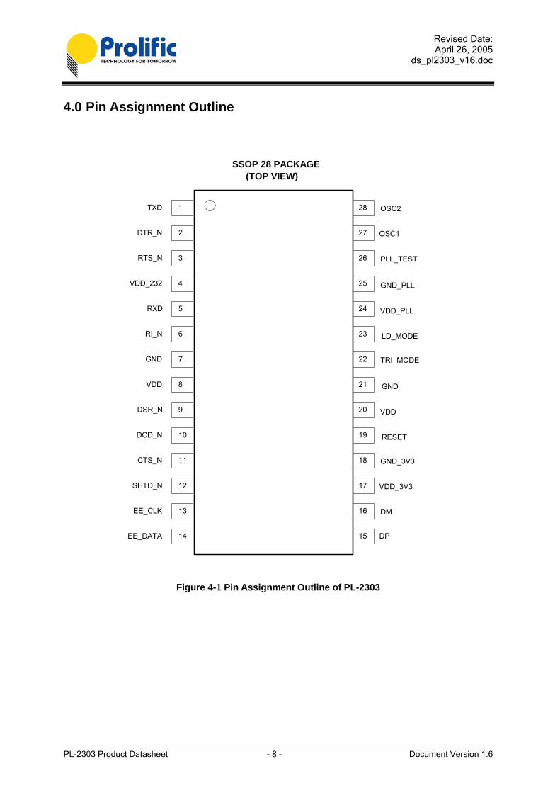
1 TXD O Data output to Serial port 2 DTR_N O Data Terminal Ready, active low 3 RTS_N O Request To Send, active low 4 VDD_232 P RS-232 VDD. The RS-232 output signals (Pin 1 ~ Pin 3) are
designed for 5V, 3.3V or 3V operation. VDD_232 should be connected to the same power level of the RS-232 interface. (The RS-232 input signals are always 5V~3V tolerant.) Note: This document version only provides 5V DC characteristic information. Refer to future revisions for updates.
5 RXD I Data input from Serial Bus 6 RI_N I Ring Indicator, active low 7 GND P Ground 8 VDD P Power 9 DSR_N I Data Set Ready, active low
10 DCD_N I Data Carrier Detect, active low 11 CTS_N I Clear To Send, active low 12 SHTD_N O Shut Down RS232 Transceiver 13 EE_CLK I/O During Reset, this pin is input for simulation purpose. During
normal operation, this pin is Serial ROM clock 14 EE_DATA I/O Serial ROM data signal 15 DP I/O USB DPLUS signal 16 DM I/O USB DMINUS signal 17 VDD_3V3 P 3.3V power for USB transceiver 18 GND_3V3 P 3.3V ground 19 RESET I System Reset 20 VDD P Power 21 GND P Ground 22 TRI_STATE I Tri-State
This pin is referred after reset. High: RS-232 output inactive during Suspend. Low: RS-232 output tri-state during Suspend.
23 LD_MD/ SHTD
I/O Load Mode/SHTD This pin is input during reset. Pull high with a 220K resistor to indicate the heavy load USB device (500mA). Pull down with a 220K resistor to indicate the light load USB device 100mA). After reset, this pin becomes output. It output the inverse of SHTD_N.
24 VDD_PLL P 5V power for PLL 25 GND_PLL P Ground for PLL 26 PLL_TEST I PLL test mode control 27 OSC1 I Crystal oscillator input 28 OSC2 O Crystal oscillator output
Type: I – Input signal O – Output signal I/O – Bi-directional signal P – Power/Ground
PL-2303 Product Datasheet - 9 - Document Version 1.6
Revised Date: April 26, 2005
ds_pl2303_v16.doc
6.0 Data Formats & Programmable Baud Rate Generator The PL2303 controller supports versatile data formats and has a programmable baud rate generator.
The supported data formats are shown on Table 6-1. The programmable baud rate generator supports
baud rates up to 1.2M bps as shown in Table 6-2.
Table 6-1 Supported Data Formats Description
Stop bits 1 1.5 2
Parity type None Odd Even Mark Space
Data bits 5, 6, 7, 8, or 16
Table 6-2 Baud Rate Setting dwDTERate Baud Rate 0012C000h 1228800 000E1000h 921600 00096000h 614400 00070800h 460800 00038400h 230400 0001C200h 115200 0000E100h 57600 00009600h 38400 00007080h 28800 00004B00h 19200 00003840h 14400 00002580h 9600 00001C20h 7200 000012C0h 4800 00000E10h 3600 00000960h 2400 00000708h 1800 000004B0h 1200 00000258h 600 0000012Ch 300 00000096h 150 0000004Bh 75
PL-2303 Product Datasheet - 10 - Document Version 1.6
Revised Date: April 26, 2005
ds_pl2303_v16.doc
7.0 External EEPROM and Device Configuration PL-2303 allows storing the configuration data in an external EEPROM. After reset, the first two bytes of
EEPROM are checked. If the value is 067Bh, the EEPROM is valid and the contents of the EEPROM
are loaded as the chip’s default parameters. Otherwise, the chip’s default setting is used. The content
of EEPROM is shown in table below.
The Device Configuration Register is used to control some vendor-specific functions. The meaning of
each bit in Device Configuration Register is shown in Table 7-2. Reserved and unused pins always set
to the default value.
Table 7-1 EEPROM Contents Bytes Name Description
1:0 EECHK When the EEPROM is programmed, these two bytes is configured as 067B. After reset, they will be checked for the value. If matched, the following information will be loaded as the default parameters.
3:2 VID USB Vendor ID 5:4 PID Product ID 7:6 RN Release number (BCD)
10:8 DCR Device Configuration Register
Table 7-2 Device Configuration Register Name Bits Definition Default
23 RESERVED Reserved 0 22 TRI_OUT RS-232 Output Tri-state:
1: RS-232 output tri-state 0: RS-232 output in output mode
0
21 RW_MODE Remote Wakeup Mode: 0: When engages remote wakeup, the device issues disconnect signal 1: When engages remote wakeup, the device issues resume signal
1
20 WURX Enable Wake Up Trigger on RXD: 0 – Disabled; 1 – Enable Wake Up Trigger on RXD state changes.
0
19 WUDSR Enable Wake Up Trigger on DSR: 0 – Disabled; 1 – Enable Wake Up Trigger on DSR state changes.
0
18 WURI Enable Wake Up Trigger on RI: 0 – Disabled; 1 – Enable Wake Up Trigger on RI state changes.
1
17 WUDCD Enable Wake Up Trigger on DCD: 0 – Disabled; 1 – Enable Wake Up Trigger on DCD state changes.
0
PL-2303 Product Datasheet - 11 - Document Version 1.6
Revised Date: April 26, 2005
ds_pl2303_v16.doc
Name Bits Definition Default 16 WUCTS Enable Wake Up Trigger on CTS:
0 – Disabled; 1 – Enable Wake Up Trigger on CTS state changes.
0
15 RESERVED Always set to one 1 14 RESERVED Always set to zero 0 13 RESERVED Always set to zero 0 12 RW_INH Remote Wake Inhibit:
1 – Inhibit the USB Remote Wakeup function 0 – Enable the USB Remote Wakeup function
0
11:6 RESERVED Always set to zero 0 5:4 RTSM RTS Control Method:
00b – RTS is controlled by ControlBitMap. Signal is active low; 01 – RTS is controlled by ControlBitMap. Signal is active high; 10 – Drive RTS active when Downstream Data Buffer is NOT EMPTY; otherwise Drive RTS inactive. 11 – Drive RTS inactive when Downstream Data Buffer is NOT EMPTY; otherwise Drive RTS active.
0
3:1 RESERVED Always set to zero 0 0 RSPDM RS-232 Transceiver Shut-Down Mode:
1: Shut down the transceiver when USB SUSPEND is engaged 0: Do not shut down the transceiver even when USB SUSPEND is engaged
1
PL-2303 Product Datasheet - 12 - Document Version 1.6
Revised Date: April 26, 2005
ds_pl2303_v16.doc
8.0 Electrical, Temperature & Timing Characteristics 8.1 Absolute Maximum Ratings
Table 8-1 Absolute Maximum Ratings
Items Ratings Power Supply Voltage -0.3 to 6.0 V Input Voltage -0.3 to VDD+0.3 V Output Voltage -0.3 to VDD+0.3 V Storage Temperature -55 to 150 oC
8.2 DC Characteristics
Table 8-2 DC Characteristics Parameter Symbol Min Typ Max Units
Power Supply Current IDD 0.5 19 24 mA Input Voltage Low High
VIL
VIH
--
0.7* VDD
-- --
0.3* VDD
--
V V
Output Voltage Low High
VOL
VOH
--
3.5
-- --
0.4 --
V V
Schmitt Trigger Threshold Voltage*1 Negative going Positive going
Vt-
Vt+
-- --
1.10 1.87
-- --
V V
Output Voltage, 3.3V*2
Low High
VOL
VOH
--
2.4
-- --
0.4 --
V V
Input Leakage Current IL -1 -- 1 uA Tri-state Leakage Current Ioz -10 -- 10 uA Input Capacitance CIN -- 3 -- Pf Output Capacitance COUT -- 3 -- Pf Bi-directional Buffer Capacitance CBID -- 3 -- Pf Operating Voltage Range -- 4.4 5 5.25 V Suspend Current ISUS -- 400 490 uA
*1. RS232 pins RXD_I, RI_I, DSR_I, DCD_I, CTS_I are 5V TTL Schmitt Trigger inputs. *2. RS232 pins TXD, DTR_N, RTS_N are 3.3V tri-state outputs.
8.3 Clock Characteristics
Table 8-3 Clock Characteristics Parameter Min Typ Max Units
Frequency of Operation 11.976 12.000 12.024 MHz
Clock Period 83.1 83.3 83.5 ns
Duty Cycle 45 50 55 %
PL-2303 Product Datasheet - 13 - Document Version 1.6
Revised Date: April 26, 2005
ds_pl2303_v16.doc
8.4 Temperature Characteristics
Table 8-4 Temperature Characteristics
Parameter Symbol Min Typ Max Unit Operating Temperature -- -40(1) -- 85(1) oC Junction Operation Temperature TJ -40 25 115 oC
Note: (1) – Test condition: Baud rate 115200 bps loop testing (4096 bytes/loop, random/fix 0xFF data transfer) over 30 minutes.
8.5 USB Transceiver Characteristics
Table 8-5 USB Transceiver Characteristics Parameter Symbol Min Typ Max Units
Rise and Fall Times: (10%─90%) (90%─10%)
TR
TF
4 4
8 8
15 15
ns ns
Cross Point VCR 1.3 -- 2.0 V
Output Impedance RD 23 28 33 ohm High Level Output VOH 2.8 -- -- V
Low Level Output VOL -- -- 0.7 V
High Level Input VIH 2.0 -- -- V
Low Level Input VIL -- -- 0.8 V
Note: CL: 50pf
8.6 EEPROM Timing Diagram
8.6.1 Byte Write Timing
Figure 8-1 Byte Write Timing Diagram
PL-2303 Product Datasheet - 14 - Document Version 1.6
Revised Date: April 26, 2005
ds_pl2303_v16.doc
8.6.2 Selective Read Timing
Figure 8-2 Selective Read Timing Diagram
8.7 Reset Timing Diagram
Figure 8-3 Reset Timing Diagram
Table 8-6 Power-On Reset
PL-2303 Product Datasheet - 15 - Document Version 1.6
Revised Date: April 26, 2005
ds_pl2303_v16.doc
9.0 Outline Diagram 9.1 SSOP28 Package
Table 9-1 Package Dimension
Millimeter Inch Symbol Min Nom Max Min Nom Max
b 0.22 0.38 0.009 0.015 E 7.40 7.80 8.20 0.291 0.307 0.323 E1 5.00 5.30 5.60 0.197 0.209 0.220 L 0.55 0.75 0.95 0.021 0.030 0.037
R1 0.09 0.004 D 9.9 10.2 10.5 0.390 0.402 0.413 A 2.0 0.079 e 0.65 0.0256 L1 1.25 0.050 A1 0.05 0.020 A2 1.65 1.75 1.85 0.065 0.069 0.073
Figure 9-1 Outline Diagram of PL-2303 SSOP28
PL-2303 Product Datasheet - 16 - Document Version 1.6
Revised Date: April 26, 2005
ds_pl2303_v16.doc
10.0 Reel Packing Information 10.1 Carrier Tape (SSOP-28)
Figure 10-1a SSOP28 Carrier Tape
Notes:
1. 10 sprocket hole pitch cumulative tolerance ±0.2 2. Camber not to exceed 1mm in 100mm. 3. Material: Black Polystyrene. 4. Ao and Bo measured on a plane 0.3mm above the bottom of the pocket. 5. Ko measured from a plane on the inside bottom of the pocket to the top surface of the carrier. 6. Pocket position relative to sprocket hole measured as true position of pocket, not pocket hole. 7. IC quantity per one reel: 1,000 (min) ~ 2,000 (max)
Figure 10-1b IC Reel Placements
PL-2303 Product Datasheet - 17 - Document Version 1.6
Revised Date: April 26, 2005
ds_pl2303_v16.doc
10.2 Reel Dimension
Figure 10-2 Reel Dimension
Table 10-2 Reel Part Number Information
Part Number Normal Hub Width
W1 +0.3mm -0.2mm
W2 Max
RD33008SW-T + RD33008SW-T 16mm 16.8mm 22.2mm
11.0 Ordering Information Table 11-1 Ordering Information
Part Number Package Type PL-2303 28-pin SSOP
PL-2303 Product Datasheet - 18 - Document Version 1.6