Plasma display panels: physics, recent developments and key issues This article has been downloaded from IOPscience. Please scroll down to see the full text article. 2003 J. Phys. D: Appl. Phys. 36 R53 (http://iopscience.iop.org/0022-3727/36/6/201) Download details: IP Address: 132.66.223.86 The article was downloaded on 19/04/2010 at 10:37 Please note that terms and conditions apply. View the table of contents for this issue, or go to the journal homepage for more Home Search Collections Journals About Contact us My IOPscience
Transcript
Plasma display panels: physics, recent developments and key issues
This article has been downloaded from IOPscience. Please scroll down to see the full text article.
2003 J. Phys. D: Appl. Phys. 36 R53
(http://iopscience.iop.org/0022-3727/36/6/201)
Download details:
IP Address: 132.66.223.86
The article was downloaded on 19/04/2010 at 10:37
Please note that terms and conditions apply.
View the table of contents for this issue, or go to the journal homepage for more
Home Search Collections Journals About Contact us My IOPscience
Received 29 August 2002Published 26 February 2003Online at stacks.iop.org/JPhysD/36/R53
AbstractIn this paper, we describe the principles of operation of a plasma displaypanel (PDP) and the physical mechanisms controlling the performances of aPDP in terms of light emission efficiency, lifetime and image quality.Emphasis is put on the physics of the plasma occurring in a PDP cell, on thedischarge optimization, and on the analysis of recent results provided byexperimental and numerical diagnostic tools. We focus on alternativecurrent PDPs, where the plasma is generated by a dielectric barrierdischarge, the configuration adopted by most PDP companies. The recentimprovements and the remaining research issues are discussed.
1. Introduction
A plasma display panel (PDP) is essentially a matrix of sub-millimetre fluorescent lamps which are controlled in a complexway by electronic drivers. Each pixel of a PDP is composed ofthree elementary UV emitting discharge cells. The UV light isconverted into visible light by phosphors in the three primarycolours. The plasma in each cell of an alternative current(AC) PDP is generated by dielectric barrier discharges (DBDs)operating in a glow regime in a rare gas mixture (typically500 Torr, 100 µm gap). The AC voltage is rectangular, withfrequency of the order of 100 kHz, and rise time of about200–300 ns. In the ON state, a current pulse of less than 100 nsduration flows through the cell at each half cycle.
PDPs have recently achieved good performance and theirimage quality can now compete with that of cathodic ray tubes(CRTs). PDPs up to 60 in. in diagonal have been demonstrated,some with high resolution. According to Standford Resources[1], more than 300 000 PDPs were sold worldwide in 2001and the market should grow to 6 million units in 2007.The sales should switch from a business-dominated market(corporate board-room, public display applications) in 2001 toa television-dominated market in 2007. This prediction willbecome true only if the companies succeed in their effortstoward cost-reduction and if the PDP technology can keep
up with competing technology such as liquid crystal displays(LCDs) and organic light emitting diodes (OLEDs). Althoughmost of the LCD production is for diagonal sizes below20 in., it now seems that LCDs will certainly overtake PDPsfor TVs up to 30 in., and LCD manufacturers are activelyworking on larger sizes [2]. OLED is a younger but verypromising technology and may become another competitor inthe future. The success of PDPs will depend on cost-reductionin the different fabrication steps and on some technologicalimprovements that must come out of the research labs intime [2].
In this paper we describe the basic mechanisms occurringin an AC PDP cell and the physics issues related to performanceimprovement. We also present the trends in the research towardbetter performance.
Section 2 contains a brief history of PDP research,and describes the characteristics of the recent PDPs andthe needs for improvements. The principles of PDPoperations (operating conditions, addressing methods) aredescribed in section 3, with a brief sub-section on PDPmanufacturing. Efficiency and lifetime issues (role of thegas mixture, operating conditions, materials) are discussedin section 4. Section 5 presents recent experimental andmodelling diagnostics of the discharge plasma in a PDP cell.Recent research trends towards better performance (mainlyrelated to efficiency) are summarized in section 6.
The use of discharge plasmas for information display startedin the early 1950s, with the numeric indicator tube developedby Burroughs. This tube used the light from the negativeglow around cathodes each shaped in the form of a numeral[3]. The PDP was invented in the 1960s at the CoordinatedScience Laboratory at the University of Illinois where Bitzerand Slottow were developing displays for educational purpose.The idea was first to use a matrix of pixels at the intersectionsof line and column electrodes and to fire light emitting gasdischarges at selected pixels. A glow discharge can be both anexcellent switch and an efficient light source and this explainsthe persistence of researchers and companies during almostfour decades to seek the goal of hang-on-the-wall colourtelevision displays with diagonals up to 60 in. Developingthe initial idea, Bitzer and Slottow realized the need for aninsulating impedance at each discharge site. They consideredthe use of resistors, the eventual use of a resistive sheet, andfinally the possibility of using a capacitive impedance insteadof a resistive impedance. The use of resistors in series witheach pixel led to the development of DC PDPs. The advantageof the capacitive impedance was that the capacitance could bepart of the panel structure in a very simple way (dielectric layersabove the electrodes) and should be easy to fabricate. Displayswith capacitive impedance in series can obviously not be drivenwith DC voltages and this led to the concept of AC PDPs [4].Bitzer and Slottow realized only later that the use of a capacitivecoupling had other very important consequences and providedthe inherent memory properties of AC PDPs. The history ofthis discovery is described in details by Slottow [5]. Otherinformation on the early development of PDPs can be foundin the review papers by Weber [6], Michel [7], and Sobel [8].
The initial PDPs were monochrome displays wherePenning Ne–Ar mixtures (typically 0.1% Ar in Ne) wereused and the light emitted by the discharges was due to thecharacteristic red–orange emission of neon. These displayswere used for displaying complex technical informationfor various professional and military purposes. Researchon colour PDPs started in the mid-1970s, and the firstcommercially available colour displays appeared in the late1990s. In colour plasma displays, the gas mixture (Xe–Neor Xe–Ne–He) emits UV photons which excite phosphorsin the three fundamental colours. Each pixel is thereforeassociated with three micro-discharge cells. Various designs ofplasma display have been proposed in the last 30 years. Threeconcepts were dominant till the end of the 1990s: the alternativecurrent matrix (ACM) sustain structure, the alternative currentcoplanar (ACC) sustain structure, and the direct current withpulse-memory drive PDP. In the ACM structure the micro-discharges take place at the intersection of line and columnelectrodes covered by a dielectric layer, as in the originalidea of Bitzer and Slottow. In the ACC structure (also calledTSD, for three electrode surface discharge) developed in theearly 1980s [9, 10], the sustain discharges occur betweensets of parallel electrodes on the same plate, and addressingis provided by electrodes on the opposite plate, which areorthogonal to the coplanar electrodes. The initial design ofthis three-electrode structure was of a transmitting type, i.e. thedischarge was behind the phosphor and the visible light was
transmitted through the phosphor. A convincing (with respectto performance) ACC design was achieved only in a reflectiontype display that was developed in 1989 [10, 11]. In thisstructure, which is now the standard structure, the discharge isin front of the phosphor and the visible light is seen directly.The ACC structure has been recently adopted by most of thecompanies. Note that Dick and Biazzo [12, 13] had proposedin the 1970s the interesting concept of single substrate matrixor coplanar PDPs where all the electrodes are on the sameglass plate. The DC PDP with pulse-memory drive [14, 15]has received considerable attention till the middle of the 1990s[16] and the feasibility of a 42 in. DC PDP was demonstrated.However, the performances (lifetime and efficacy) of DC PDPswere lower than those of AC PDPs, and this technology isnow only marginally studied and developed. An importantresearch effort had however been invested in DC PDPs andsome of the concepts and ideas developed within this frameare worth remembering (see, e.g. the works on positive columndischarges [17, 18] and Townsend discharges [19] for DCPDPs). The DC PDP will not be further discussed in this paper.
AC PDPs have now achieved a high level of performance.The first colour displays in the early 1990s had very lowluminous efficacy (less than 1 lumen per Watt—lm W−1) andlow contrast. At the time this review is written, manufacturersreport 1–2 lm W−1 efficacy for commercially available PDPsand 2–3 lm W−1 for laboratory samples [1]. The reportedluminance is between 500 and 700 cd m−2 for 42–63 in.PDPs and the announced contrast ratios are 3000 : 1 in darkviewing conditions and 120 : 1 in bright light conditions. Thereported lifetime can reach 30 000 h. The above numbersare cited by different manufacturers, and, since performancemeasurements are not yet standardized, it is difficult to knowexactly what has been measured. From these numbers,however, it appears that an important research effort is stillneeded to improve the luminous efficacy which remains lowcompared to CRTs (about three times lower). An improvementof luminous efficacy will lead to cost reduction since it shouldlead to a decrease of the electronic drivers power requirementsand thus of the driver cost, which is a large part of the totalcost of a PDP. The trends in the research to achieve thisgoal is in the direction of more complex electrode shapes(within the ACC concept), optimization of cell geometry andgas mixture, material research (protective and emissive layer,phosphors) and optimization of addressing and sustainingschemes. In spite of the relatively large lifetime announced bythe manufacturers, it seems that lifetime is still an issue. Theinitial brightness of a PDP is high (more than 500 cd m−2),but the display quickly loses brightness over time [2]. Thisis due to the degradation of activated phosphors (the mostvulnerable phosphor being the blue emitting one). Thedecrease of the luminance of a PDP can be as large as 10%in 5000 h [20] in normal operating conditions (the lifetime ofthe panel corresponds to a 50% decay of the luminance). Theoverall lifetime of a PDP also depends on the lifetime of theprotective and emissive MgO layer and this parameter is notcompletely controlled. Another remaining issue concerningpanel performance is related to image quality. Due to the waythe grey scale is formed in a PDP, visible artefacts can formon the screen, especially when moving objects are displayed.These artefacts (called false contours) are corrected with
R54
Topical Review
sophisticated addressing schemes and dynamic false contourreducing methods [21]. Research is however still needed onthis aspect.
Understanding the basic physics of the plasma dynamics,electron energy deposition and plasma–surface interactions isan essential part of the improvement of this technology. Thisis confirmed both by the dramatic increase in the number ofpapers published by research institutions on this topic in thelast five years, and by the increasing number of high qualityscientific papers recently published by company researchers inconference proceedings or in scientific journals.
3. DBDs for AC PDPs: principles and keyparameters
Almost all the PDP companies have now adopted the AC PDP.In AC PDPs each cell consists of a microscopic DBD, i.e.the electrodes are covered with a dielectric layer 20–40 µmthick. Historically, DBDs have been applied to ozoneproduction [22] in the mid 19th century, much before theiruse in displays. The application of DBD to the generationof VUV excimer radiation was proposed by Tanaka [23] in1955. DBDs at atmospheric pressure can produce intenseultraviolet radiation that can be used to break molecularbonds and initiate photophysical and photochemical processes,and to modify surface properties. There are thus numerouspotential applications of DBDs to material processing, thin-film deposition, pollution control, sterilization, and of courselighting (see Kogelschatz et al [22] and references therein).In the applications above, the DBDs generally operate at highpressure, for gap lengths of the order of 1 mm to a few cm.Under these large pd (pressure × gap length) conditions, thedischarges operate in a streamer regime. Random transientfilaments form in the electrode gap and are quenched dueto the current limitation by the localized charge build-up onthe dielectric layers. The applied voltage must change signperiodically in order to generate new discharges and newfilaments. The voltage frequency is between 50 Hz and severalhundred kHz in most applications. The limitation of the currentdue to the capacitive layers allows a good control of the powerdeposition in the volume, which would be impossible withmetal electrodes in these atmospheric pressure and large gaplength conditions.
In DBDs for PDPs, the electrode gap length is short, ofthe order of 100 µm, the pressure p is about 500 Torr and suchthat the pd product is of the order of a few Torr cm. For thesesmall pd values, the discharges do not operate in a streamerregime but in a glow discharge regime. It is essential to operatein this regime because the ability to control each dischargeseparately and the reproducibility of the discharges are ofparamount importance in a PDP. In this section we presentthe principles and operating conditions of a PDP. Emphasis isput on the physics but some of the more technological aspects(e.g. driving of a PDP panel, pixel size, high definition, etc)are also briefly discussed. The technological issues imposethe constraints on the operating conditions of a PDP (e.g.addressing speed and response time of cell) and this is why aperfect understanding and control of the physics in a dischargecell is necessary.
3.1. Principles and operating conditions of AC PDPs
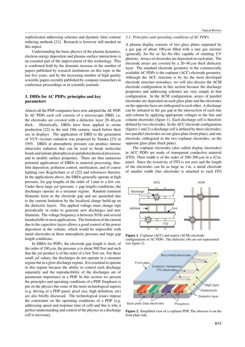
A plasma display consists of two glass plates separated bya gas gap of about 100 µm filled with a rare gas mixture(generally Xe–Ne or Xe–Ne–He) capable of emitting UVphotons. Arrays of electrodes are deposited on each plate. Theelectrode arrays are covered by a 20–40 µm thick dielectriclayer. The standard electrode geometry in the commerciallyavailable AC PDPs is the coplanar (ACC) electrode geometry.Although the ACC structure is by far the most developedelectrode structure nowadays, we will also discuss the ACMelectrode configuration in this section because the dischargeproperties and addressing schemes are very simple in thatconfiguration. In the ACM configuration, arrays of parallelelectrodes are deposited on each glass plate and the electrodeson the opposite faces are orthogonal to each other. A dischargecan be initiated in the gas gap at the intersection of each lineand column by applying appropriate voltages to the line andcolumn electrodes (figure 1). Each discharge cell is thereforedefined by two electrodes. In the ACC electrode configuration(figures 1 and 2) a discharge cell is defined by three electrodes:two parallel electrodes on one glass plate (front plate), and oneelectrode, orthogonal to the two coplanar electrodes, on theopposite glass plate (back plate).
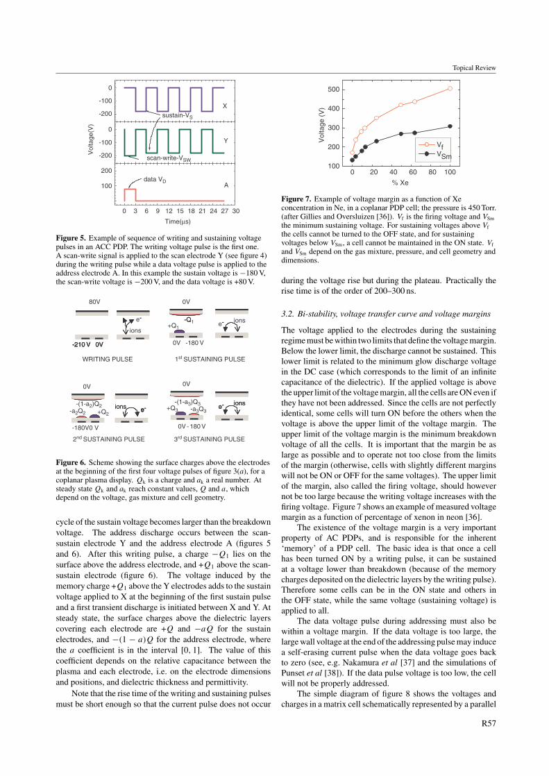
The coplanar electrodes (also called display electrodes)in ACC PDPs are made of transparent conductive material(ITO). Their width is of the order of 200–300 µm in a 42 in.panel. Since the resistivity of ITO is not zero and the lengthof the electrodes can be as large as 1 m, a metal electrodeof smaller width (bus electrode) is attached to each ITO
ITO
busaddress
ACC ACM
discharge
ITO
Figure 1. Coplanar (ACC) and matrix (ACM) electrodeconfigurations of AC PDPs. The dielectric ribs are not represented(see figure 2).
Front plateCoplanar, transparent
ITO electrodes
Bus (metal) electrodes
Back plate Data electrodes
Dielectricrib
Dielectric layer
Phosphors
MgO layer
Coplanar, transparentITO electrodes
Bus (metal) electrodes
Figure 2. Simplified view of a coplanar PDP. The observer is on thefront plate side.
R55
Topical Review
electrode to maintain a constant potential along the coplanarITO electrodes. The data (or address) electrodes are metallicand their width is of the order of 80 µm in standard PDPs.Successive pairs of coplanar electrodes are separated bydielectric barrier ‘rib’ structures formed on the inner surfacesof the glass plates. A dielectric layer of thickness between20 and 40 µm covers the address and coplanar electrodes.A MgO layer (about 500 nm) is deposited on the dielectricsurface above the coplanar electrodes to protect the dielectricfrom sputtering and to provide large secondary electronemission under ion impact. Phosphors in the three colours aredeposited above the data electrodes and on the dielectric ribs(figure 2). The ribs are generally parallel stripes separatingthe rows of the panel, as in figure 2, but a recent trend isto close the cell in both directions. For example, plasmadisplays with ‘WAFFLE’ ribs [24, 25], or ‘DelTA’ ribs [26, 27]have been recently built (see photos of the WAFFLE structurein section 3.5, and diagrams of the WAFFLE and DelTAstructures in section 6). This improves the collection of VUVphotons in a given cell and decreases cross-talk effects. Usefullight emitted by phosphors exits PDP through the coplanarelectrode face. The discharge also emits visible emission,mainly red–orange light from neon. For improving the primarycolour purity, some manufacturers insert capsulated colourfilters on the front plate prior to the dielectric layer formation[28] (these filters are not represented in figure 2).
Addressing a cell in the ACM structure is relatively simple(figure 3). A sustaining AC voltage, VS is constantly appliedbetween the line and column electrodes. The amplitude of thesustaining voltage must be smaller than the breakdown voltageof the discharge cells.
In order to turn a cell to the ON state, a voltage pulse(writing pulse) is applied between the line and column definingthe selected cell, as shown in figure 3. The amplitude ofthis voltage pulse is larger than the breakdown voltage of thecells. A glow discharge forms and is quickly quenched by thecharging of the dielectric layers which creates a voltage acrossthe gas gap opposing the voltage across the electrodes. At theend of this ‘writing’ pulse, the charges on the dielectric surfacesabove each electrode are −Q and +Q. At the beginning of thenext half cycle of the sustaining voltage, the voltage due to the
OFF
Writing Erasing
V
Sustaining
ON OFF
Voltage
Current
OFF
Writing Erasing
Vs
Sustaining
ON OFF
Voltage
Current
Time
0 0+++
---
-Q +Q---
+++
+Q -Q+++
---
-Q +Q 0 00 0+++
---
-Q +Q---
+++
+Q -Q+++
---
-Q +Q 0 0
Figure 3. Example of a sequence of writing, sustaining, and erasingpulses in an ACM PDP. The voltage pulses, current pulses, andcharges on the dielectric surfaces after each pulse are shown (afterSlottow [35]).
charge on the dielectric surfaces above the dielectrics now addsto the applied voltage and the gas gap voltage (or ‘cell voltage’)is again above breakdown. A new discharge pulse is initiated.In ACM colour PDPs developed in the 1990s [29, 30], thegas mixtures was Xe(10%)–Ne at pressures between 500 and600 Torr and the gas gap length 100 µm. With a 500 nm MgOlayer above the dielectric surfaces, the sustaining voltage wasof the order of 150 V, and the writing voltage between 200 and250 V. The duration of the current pulses in these conditionsis of the order of 20–50 ns (see, e.g. Meunier et al [31],Punset et al [32]). In the scheme of figure 3, the charges onthe dielectric surfaces are (−Q, +Q) after the writing pulse,(+Q, −Q) after the first sustaining pulse, and so on. Thiscorresponds to the ideal case where a steady state regime isreached immediately after the writing pulse. This is possibleif the writing voltage is carefully chosen, otherwise the surfacecharges evolve to this steady state after a few sustaining pulses.Note that the charge transferred during the writing pulse isQ while the charge transferred during the sustaining pulse is2Q. Erasing is obtained by applying a voltage pulse smallerthan the sustaining voltage and such that the charge transferredduring the pulse is Q instead of 2Q. After the erasing pulse thecharges on the surface at the beginning of the next half cycleare zero. The writing, sustaining and erasing pulse voltagescan be easily chosen if one knows the ‘voltage transfer curve’of the cell. These curves and the stability conditions of thesustaining regime have been analysed by Slottow et al [33],Sahni et al [34], and Slottow [35] for the ACM structure. Webriefly discuss these questions in section 3.2.
Addressing a coplanar cell is more complicated and thereare more possible addressing schemes for the ACC structurethan for the ACM since the coplanar cell is defined by threeelectrodes instead of two (see figure 4). When a coplanar cell isin the ON state, a succession of discharge pulses occur betweenthe two coplanar electrodes due to the rectangular AC voltageconstantly applied between pairs of coplanar electrodes (thelines of the display). As in the ACM case, the amplitude ofthis sustaining voltage is below the breakdown voltage of thecell. The third electrode (on the back plate) is called ‘dataelectrode’ or ‘address electrode’ and is used to turn a givencell to the ON state or to the OFF state.
This is illustrated in figure 5 where a first voltage pulseis applied between the A electrode (data electrode) andY electrode (scan-sustain electrode) and is followed by severalsustain pulses. As in the ACM case, the role of the writingpulse is to depose surface charges on the dielectric layersabove the sustain electrodes so that the voltage drop in the gasabove the sustain electrodes at the beginning of the next half
e
h
wd
X Y
A
Figure 4. Simplified scheme of a coplanar cell with definitions ofnotations used in the text. A is the address electrode, X and Y thesustain electrodes, Y the scan electrode.
R56
Topical Review
sustain-VS
X
scan-write-VSW
Y
Vol
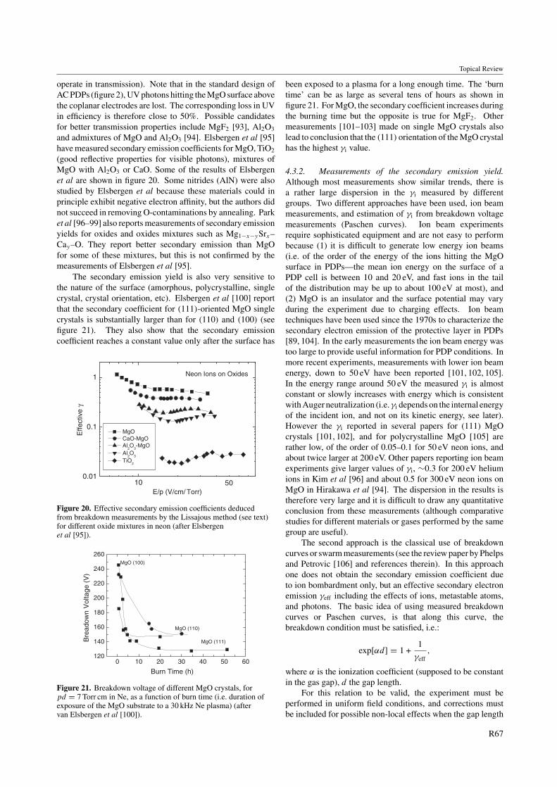
tage
(V)
data VDA
Time(µs)
-200
-100
0
-200
-100
0
0 3 6 9 12 15 18 21 24 27 30
100
200
Figure 5. Example of sequence of writing and sustaining voltagepulses in an ACC PDP. The writing voltage pulse is the first one.A scan-write signal is applied to the scan electrode Y (see figure 4)during the writing pulse while a data voltage pulse is applied to theaddress electrode A. In this example the sustain voltage is −180 V,the scan-write voltage is −200 V, and the data voltage is +80 V.
e-
ions
-210 V 0V
ionse-+Q1
-Q
0V -180 V
0V80V
e-ions-a2Q2
-a3Q3
-180V0 V
0V
0V - 180 V
0V
ionse-
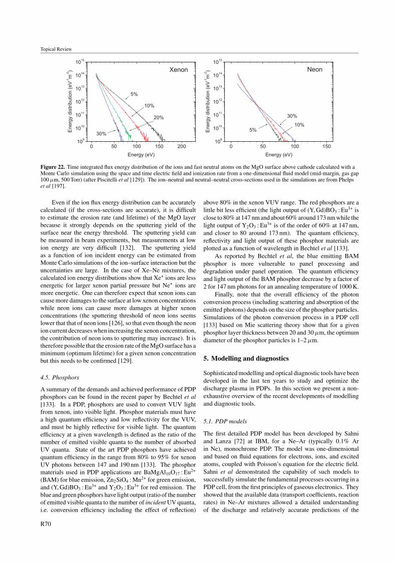
WRITING PULSE 1st SUSTAINING PULSE
-
-210 V 0V-210 V 0V
--Q1
e-ions ee+Q2+Q3
-(1-a2)Q2-(1-a3)Q3 ionse-e-
2nd SUSTAINING PULSE 3rd SUSTAINING PULSE
Figure 6. Scheme showing the surface charges above the electrodesat the beginning of the first four voltage pulses of figure 3(a), for acoplanar plasma display. Qk is a charge and ak a real number. Atsteady state Qk and ak reach constant values, Q and a, whichdepend on the voltage, gas mixture and cell geometry.
cycle of the sustain voltage becomes larger than the breakdownvoltage. The address discharge occurs between the scan-sustain electrode Y and the address electrode A (figures 5and 6). After this writing pulse, a charge −Q1 lies on thesurface above the address electrode, and +Q1 above the scan-sustain electrode (figure 6). The voltage induced by thememory charge +Q1 above the Y electrodes adds to the sustainvoltage applied to X at the beginning of the first sustain pulseand a first transient discharge is initiated between X and Y. Atsteady state, the surface charges above the dielectric layerscovering each electrode are +Q and −aQ for the sustainelectrodes, and −(1 − a)Q for the address electrode, wherethe a coefficient is in the interval [0, 1]. The value of thiscoefficient depends on the relative capacitance between theplasma and each electrode, i.e. on the electrode dimensionsand positions, and dielectric thickness and permittivity.
Note that the rise time of the writing and sustaining pulsesmust be short enough so that the current pulse does not occur
0 20 40 60 80 100
Vol
tage
(V
)
% Xe
VfVSm
100
200
300
400
500
Figure 7. Example of voltage margin as a function of Xeconcentration in Ne, in a coplanar PDP cell; the pressure is 450 Torr.(after Gillies and Oversluizen [36]). Vf is the firing voltage and VSm
the minimum sustaining voltage. For sustaining voltages above Vf
the cells cannot be turned to the OFF state, and for sustainingvoltages below VSm, a cell cannot be maintained in the ON state. Vf
and VSm depend on the gas mixture, pressure, and cell geometry anddimensions.
during the voltage rise but during the plateau. Practically therise time is of the order of 200–300 ns.
3.2. Bi-stability, voltage transfer curve and voltage margins
The voltage applied to the electrodes during the sustainingregime must be within two limits that define the voltage margin.Below the lower limit, the discharge cannot be sustained. Thislower limit is related to the minimum glow discharge voltagein the DC case (which corresponds to the limit of an infinitecapacitance of the dielectric). If the applied voltage is abovethe upper limit of the voltage margin, all the cells are ON even ifthey have not been addressed. Since the cells are not perfectlyidentical, some cells will turn ON before the others when thevoltage is above the upper limit of the voltage margin. Theupper limit of the voltage margin is the minimum breakdownvoltage of all the cells. It is important that the margin be aslarge as possible and to operate not too close from the limitsof the margin (otherwise, cells with slightly different marginswill not be ON or OFF for the same voltages). The upper limitof the margin, also called the firing voltage, should howevernot be too large because the writing voltage increases with thefiring voltage. Figure 7 shows an example of measured voltagemargin as a function of percentage of xenon in neon [36].
The existence of the voltage margin is a very importantproperty of AC PDPs, and is responsible for the inherent‘memory’ of a PDP cell. The basic idea is that once a cellhas been turned ON by a writing pulse, it can be sustainedat a voltage lower than breakdown (because of the memorycharges deposited on the dielectric layers by the writing pulse).Therefore some cells can be in the ON state and others inthe OFF state, while the same voltage (sustaining voltage) isapplied to all.
The data voltage pulse during addressing must also bewithin a voltage margin. If the data voltage is too large, thelarge wall voltage at the end of the addressing pulse may inducea self-erasing current pulse when the data voltage goes backto zero (see, e.g. Nakamura et al [37] and the simulations ofPunset et al [38]). If the data pulse voltage is too low, the cellwill not be properly addressed.
The simple diagram of figure 8 shows the voltages andcharges in a matrix cell schematically represented by a parallel
R57
Topical Review
Before current pulse
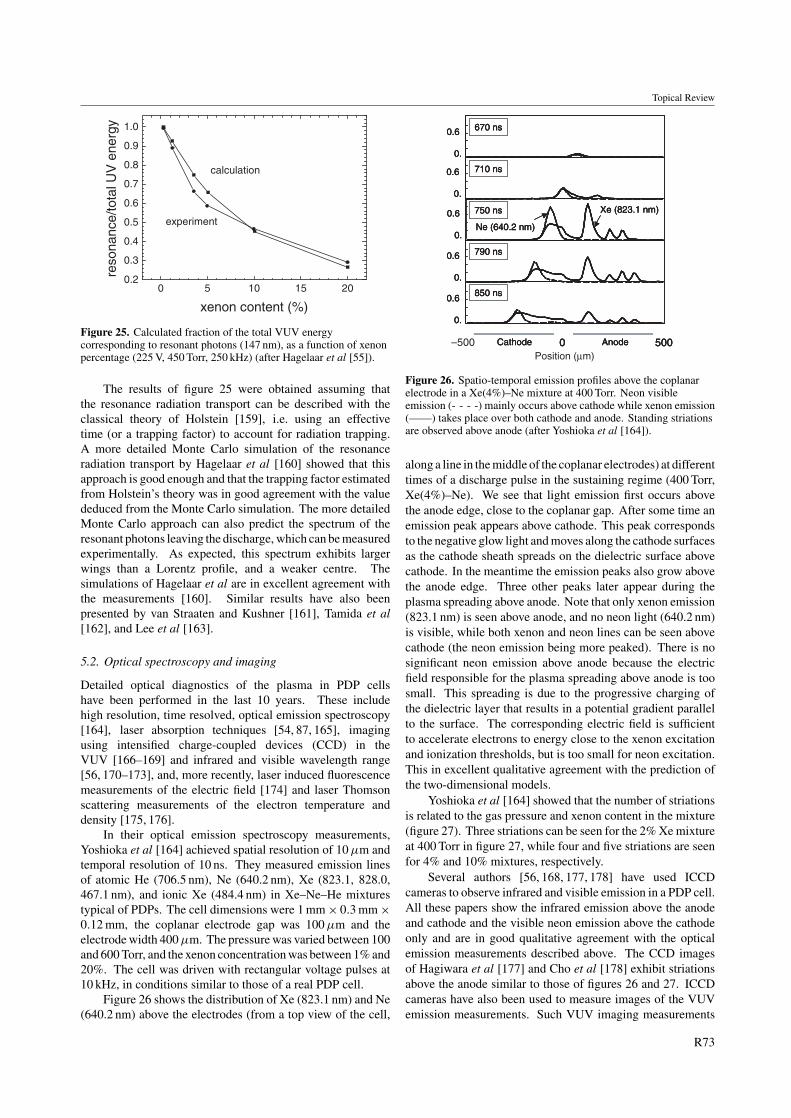
After current pulse
Vg=VS+ V W
-Q0
VS
+Q
0+Q
VS
-Q
-VW/2 -VW/2
+VW/2Vg=VS- V W=0+VW/2
Figure 8. Charges and voltages in a matrix cell before and after acurrent pulse. At steady state, in a stable sustaining regime one musthave VW = VS and the voltage across the gas gap is 2VS before thecurrent pulse and 0 after the current pulse. At the beginning of thenext voltage pulse, the voltages on the left and right electrodesswitch to VS and 0, respectively, and the voltage across the gas gapis −2VS.
plate gas gap between two equal dielectric layers of capacitanceC each. The voltages and charges are represented at thebeginning and at the end of a voltage pulse in a steady statesustaining regime. The sustaining voltage is VS. Assume thatthe voltage drop across the two dielectric layers due to thecharges −Q and +Q deposited on the dielectric surfaces byprevious discharges is −VW (i.e. −VW/2 across each). Q andC are related by: Q = CVW/2. In the discussion of theenergy per pulse below, we neglect the gas gap capacitancewith respect to the dielectric capacitance and VW is equal to thetotal voltage drop across the dielectric surfaces. If the gas gapcapacitance is not neglected, VW is slightly different from thetotal voltage drop VD (see later, the exact relation between VW
and VD) across the dielectric layers, which takes into accountthe electrostatic charges associated with the charging of thedielectric and gap capacitance in series. The voltage acrossthe gas gap before the current pulse is Vg = VS + VW. If weare in a steady state regime, the charges on the left and rightdielectric layers at the end of the current pulse must be +Q and−Q, respectively, and the new total voltage drop across thedielectric layers must be +VW (+VW/2 across each). Undernormal operating conditions, the voltage across the gas gap atthe end of the pulse, Vg = VS − VW should be 0, like in thecomplete discharge of a capacitor through a resistor. We musttherefore have VW = VS in stable operating conditions. Thechange of the voltage across each dielectric layer during thedischarge is therefore equal to VS, and the total change ofthe wall voltage �VW must be equal to 2VS. �VW = 2VS
is the stability condition. In stable conditions of operations,the voltage across the gap at the beginning of each voltagepulse is ±2VS.
The energy dissipated during a discharge pulse is
Epulse =∫
pulseVSI dt = VS
∫pulse
I dt = 2QVS = CV 2S
and the charge transferred during the pulse is �Q = 2Q =CVS. Since the equivalent capacitance of the two dielectric
100 150 200 250 300
C
VWVS
B
A
slope=2
slope=1
Cha
nge
of W
all V
olta
ge ∆
VW
(V)
Vc=Vg/K=VS+VW (V)
0
50
100
150
200
250
300
Figure 9. Example of voltage transfer curve (after Slottow [35]); thenumerical values are from Meunier et al [31]) and are obtained witha one-dimensional model in a Xe(10%)–Ne mixture. A and C aretwo stable points in the ON and OFF regimes, respectively. The twostraight lines of slope 2 define the limit of bi-stability. Theintersections of these lines with the horizontal axis corresponds tothe minimum and maximum values of VS in the bistable regime, anddefine the margin.
layers is CD = C/2, and the gas gap voltage change duringthe pulse is 2VS, the energy per pulse and charge transfer canbe written in the usual form:
Epulse = 12CD[2VS]2 and �Q = CD[2VS].
The concept of voltage transfer curve [33, 35] is very usefulto define the stable operating conditions of a PDP cell. Anexample of voltage transfer curve is shown in figure 9. Thevoltage transfer curve plots the change of the wall voltage in agiven discharge as a function of the initial voltage across thegas gap just before the discharge. The abscissa in figure 9 isactually slightly different from the gas gap voltage if the gasgap capacitance Cg cannot be neglected with respect to theequivalent capacitance of the two dielectric layers CD = C/2.Let K = CD/(CD + Cg), and let VD be the total voltage acrossthe dielectric walls. The exact definitions of the voltages usedto plot the voltage transfer curve are (see also the definitionsin Johnson et al [39], and Meunier et al [31]):
Vc = Vg
K= VS + VW,
VW = VD
K− VS(1 − K)
K= − Q
CD,
when Cg is neglected with respect to CD (i.e. K ∼ 1), we haveVc ∼ Vg and VW ∼ VD, as in the discussion related to figure 8.In typical conditions of AC PDPs, K is between 0.9 and 1. Notethat VW only accounts for the charge deposited on the dielectricby previous pulses while VD also includes the electrostaticcharges associated with the capacitive divider formed by thewall capacitor CD in series with the gap capacitor Cg.
Slottow and Petty showed that the slope of the voltagetransfer curve around the operating point must be less than 2for stable operations (see the example of figure 9). Weberet al [40, 41] defined a slightly different wall voltage input–output curve that plots the output wall voltage as a functionof input wall voltage. These curves can be used, for example,to determine the optimal values of the writing, sustaining anderasing voltage pulses of figure 3, or to analyse how the two
R58
Topical Review
stable states of the cell, the ON or OFF states respond to aperturbation. In the example of figure 9, the operating pointsfor a given value of the sustaining voltage VS are obtainedby plotting a line of slope 2 starting at abscissa VS, on thehorizontal axis [35]. There are three intersections (points A,B, and C) of this line with the voltage transfer curve. It ispossible to show that B is not stable. A is the stable point inthe ON regime, and C is the stable point in the OFF regime.If the initial wall voltage VW is in between the abscissa of Band A, it is possible to show that the operating point will moveto A, i.e. to the ON state, after a few pulses of the sustainingvoltage. If the initial wall voltage VW is in between the abscissaof C and B, the operating point will move to C, i.e. to the OFFstate, after a few pulses of the sustaining voltage. The voltagetransfer curve illustrates clearly the concept of bi-stability andallows predicting the response of the cell after a perturbation.
The discussion above was based on a simple, one-dimensional matrix geometry. In a real problem, like in thecase of a coplanar electrode configuration, the problem ismore complicated because the plasma does not necessarilycover the whole electrode area, and the voltage is not constantalong the dielectric surface. However the general ideas ofthis discussion, i.e. existence of a stability conditions and bi-stability, remain true.
3.3. Panel addressing—grey scale—priming
The principles of addressing and sustaining a coplanar cellhave been exposed in section 3.1. The question of addressingbecomes much more complicated when one has to deal withaddressing and sustaining one or several million cells at afrequency of 60 Hz (60 frames per second) and with thepossibility of displaying more than 16 million colours.
Each pixel is composed of three individual cells in thethree primary colours. It is possible to display 16.7 millionscolours (256 × 256 × 256) if each discharge cell can display256 intensity levels (‘grey scale levels’). This implies thepossibility of modulating the light emission intensity of eachdischarge cell on 256 levels. Obviously this modulation cannotbe performed by a modulation of the voltage or current ofeach discharge pulse. The grey scale is rather obtained bymodulating the number of current pulses in a given dischargecell during a TV field (16.7 ms, corresponding to 60 Hz).A binary coding is used to achieve 256 levels. Therefore, a TVfield or frame is divided into eight sub-fields where each cellcan be sustained for 1, 2, 4, . . . or 128 times a given numberof discharge pulses (see figure 10). The 256 possible levelsare obtained by turning the cell ON for any combination of theeight sub-fields, as in a binary coding. This allows varyingthe perceived intensity of the cell to any one of the 256 greyscale levels. During each of the eight sub-fields, it is thereforenecessary to reset, address and sustain the cell. The duration ofthe address period (including a reset step and an address step)is constant, and the duration of the sustain periods in the sub-fields vary in proportion of 1, 2, 4, . . . to 128. One drawbackof the binary coding is that the temporal non-uniformity ofthe light emission scheme (e.g. when changing from the level127—bits 0–6, to 128—bit level 7) is transformed into aspatial non-uniformity of the light emission pattern on theretina [21, 42]. Motional artefacts such as dynamic false
1
line 1
1 frame (16.7ms) time
sustain
addresssub-fields
reset
line 2
line N
2 4 8 16 32 64 128
Figure 10. Method of generating 256 grey levels in the ADSmethod [194]. One 16.7 ms TV-field or frame is divided intoeight sub-fields, each containing an address period (with a reset stepand an address step), and a sustain period. A given grey level istherefore coded on 8 bits. The reset and address step durations arethe same for all sub-fields. The durations of the sustain periods areproportional to 1, 2, 4, . . . , 128. All the cells of a given line areaddressed simultaneously. The different lines are addressedsequentially, as indicated by the diagonal lines. In a standard VGAdisplay with 480 lines the total time spent in addressing is about12 ms while the time spent in sustaining (i.e. time during which thedisplay emits light) is only about 5 ms.
contours may be observed when moving images are displayedon colour plasma displays. Reduction of these disturbancesis essential for the picture quality and various methods havebeen introduced to reduce motional artefacts. These methodsare described in Yamaguchi et al [21] and Weitbruch et al [42].
The driving waveform for one of the sub-fields is displayedin figure 11 in the case of the address display separated (ADS)method proposed by Shinoda [43]. In this method the cellsare first prepared during a reset step, then they are addressed(i.e. memory charges are deposited in the cells which needto be ON during this sub-field), and the addressed cells areturned ON during the sustain period (which duration dependson the sub-field). The address and display periods are thereforeclearly separated in the ADS method. Many companies usethe ADS scheme but other driving methods are possible wheresome cells may be addressed while other are sustained (AWD,address while display [44]). Within the ADS method, figure 11shows one possible reset and addressing scheme, but differentaddressing schemes are possible and are described in differentpatents.
Addressing clearly consumes a large fraction of the timeof a given TV frame since all the lines of the display mustbe addressed eight times during one frame. Assuming thatthe duration of each address pulse is τad, and that Nlines is thenumber of lines of the panel, the total time Tad necessary toaddress the display is (neglecting the reset period duration)Tad = 8Nlinesτad. Assuming that the duration of the addresspulses, τad, is 3 µs, the total addressing time Tad is 11.52 msfor a VGA display (640 rows × 480 lines). This means thatonly about 5 ms remains for the total sustain duration of a TVframe. It is possible but difficult to use address pulses shorterthan 3 µs. This is because, although the current pulse durationis short, of the order or less than 100 ns, the decay time of theplasma, which is mainly controlled by ambipolar diffusion, isof the order of a few microseconds. If the plasma density is
R59
Topical Review
RESET
address pulse
erase pulse
scan pulse
sustain pulse
write pulse
Addresselectrode
X sustainelectrode
Y1 sustainelectrode
YN sustainelectrode
Va
ADDRESS SUSTAIN
Figure 11. Example of driving waveform (ADS method [43]) for one sub-field of figure 10. The cells are addressed line by line. The samevoltage is applied to all the X electrodes. The reset period is used to set all the cells to the same state; in this example the memory chargesare first erased, all the cells are then turned ON with a write pulse, and erased again. During the address period an address pulse is sent to thecells of a given line that need to be turned ON while a scan voltage pulse is sent to the Y electrode of each line successively. Memorycharges are written on the cell when the scan pulse of a given Y electrode coincides with a pulse on the corresponding address electrode.After the cells of the whole screen have been addressed, the sustain period starts and a discharge occurs in the cells which have beenaddressed, at twice the frequency of the sustain voltage.
0 20 40 60 80 1000
200
400
600
800
Jitte
r (n
s)
Sustaining Frequency (kHz)
Figure 12. Influence of sustaining frequency on jitter (after Seguinet al [195]) in a matrix electrode display (gas gap 130 µm, gasmixture Xe(10%)–Ne, 190 V sustain voltage).
too large when the address pulse is switched off, an unwantedcurrent pulse may partially erase the charges deposited duringthe address pulse and lead to addressing failure. To ensuresuccessful addressing it is also necessary to keep the delaytime to breakdown as short as possible. It is therefore essentialto minimize the jitter.
The question of addressing failure due to jitter is importantand one of the goals of the reset period is to keep the jitter aslow as possible. Jitter is due to statistical lag time [45] of adischarge and is strongly related to the number of availableseed electrons in the cell when the address pulse is applied.Seed electrons may be missing in a cell that has not been ONfor a long time (black regions of the image).
Figure 12 shows the influence of the sustaining frequencyon jitter. It is clear on this picture that a cell which has notbeen ON for a long time will be difficult to write with a shortaddress pulse. Below 60 kHz, the slope of this curve changesabruptly because the number of charges remaining from theprevious pulse becomes too small for pulse lengths smallerthan about 10 µs to ensure a fast start of the current pulse. Thistime is related to the plasma decay due to ambipolar diffusion.Below 60 kHz, the time delay to breakdown becomes morestatistical and may depend on other sources of free electrons,e.g. metastable impact on the MgO surface [46, 47], UVphotons coming from other cells that are in the ON state,
erase pulse
ramp scan pulse
Y1 sustainelectrode
YN sustainelectrode
X sustainelectrode
Addresselectrode
erase pulse
ramp scan pulse
Y1 sustainelectrode
YN sustainelectrode
X sustainelectrode
Addresselectrode
Figure 13. Reset period using ramp voltage to allow efficientpriming while keeping good contrast ratio and control of the cellstate before addressing (after Weber [50]). If the rise time of theramp is small enough, the discharge operates in the Townsendregime (dark discharge).
release of electrons from the MgO surface. The curve offigure 12 is strongly modified if neighbour cells are ON,which indicates that UV photons coming from other cells maygenerate photoelectrons on the MgO surface. The jitter seemsto strongly depend on the crystal structure of the MgO layer.The question of the role of the surface on breakdown jitter [48]is rarely discussed in the context of PDPs [49] but may haveimportant implications for driving. The parameters controllingthe jitter, i.e. the generation of seed electrons in the cell are verypoorly known. Research is needed to study the properties ofthe MgO surface and its ability to release charges in the gasvolume.
The purpose of applying a writing pulse to all the linesduring the reset period (figure 11) is to provide enough seedelectrons in the cells to decrease current jitter and to ensure thatthe discharges start in much less than τad (e.g. 3 µs) in the cellswhich are addressed. This is called priming and the writingpulse applied during the reset period is generally a high voltagepulse (several hundreds of V). A consequence of priming witha high voltage pulse is that all the cells of the panels are turnedON at the beginning of each sub-field, i.e. eight times per TVframe, and this generates considerable discharge light. Thedark-room contrast ratio (ratio of the luminance of pixel sitesin the full intensity state to the luminance of pixel sites inthe OFF state) is strongly affected by high-voltage primingbecause even the cells in the OFF state are turned ON during
R60
Topical Review
300
200
100
15 1500
0
1.875 V/
7.5 V/
3.75 V/
0 50 100 150 200
Time (µs)
Time (µs)
1.875 V/7.5 V/ 3.75 V/
0 50 100 150 200
1500 V/
15 V/
00.2
0.4
0.6
0.8
Blu
e lig
ht (
arb.
uni
ts)
300
200
100
15 1500
0
1.875 V/
7.5 V/
3.75 V/
0 50 100 150 200
300
200
100
Vol
tage
(V
)15
1500
0
1.875 V/µs
7.5 V/µs
3.75 V/µs
0 50 100 150 200
1.875 V/7.5 V/ 3.75 V/
0 50 100 150 200
1500 V/
15 V/
00.2
0.4
0.6
0.8
1.875 V/µs7.5 V/µs 3.75 V/µs
0 50 100 150 200
1500 V/µs
15 V/µs
00.2
0.4
0.6
0.8
Figure 14. Light output for different ramp waveform (afterWeber [41]).
the reset periods. A very nice way of minimizing the amountof light emitted during priming has been introduced by Weber[41, 50]. Instead of applying a high voltage pulse for priming,Weber proposed to replace the voltage pulses in the reset periodof figure 11 by the ramp waveforms displayed in figure 13.The ramp voltage slope has to be small enough so that, assoon as the gap voltage reaches breakdown, the dischargestays in a Townsend regime, i.e. the voltage applied betweenthe Y and A electrodes continues to increase while the gasgap voltage stays constant at a value close to the breakdownvoltage (due to the continuous, slow charging of the dielectriclayers by the dark discharge current). A similar dischargeoccurs during the negative slope. This allows both a goodpriming, and a good control of the wall charges (i.e. a well-defined state of the wall charges and voltage) [41]. Figure 13shows an example of possible reset period consisting of anerase pulse, followed by one positive and one negative rampvoltage. Many variations using ramp voltages are possibleand can lead to specific addressing schemes depending on thecharges deposited on the cell walls during this period [41].The analysis of the charge transfer on the different electrodesduring the ramp is not easy, and models are very helpful toquantify this aspect [51–53].
Figure 14, from Weber [41] shows the neon light outputmeasured for different slopes of the ramp voltage (the neonlight output closely follows the current pulse [54]). The 1500and the 15 V µs−1 ramps show a rapid pulsed type of lightoutput. The 7.5, the 3.75 and the 1.875 V µs−1 ramps show alower peak intensity and correspond to a Townsend dischargewhere the light output intensity appears to have an amplitudeproportional to the ramp rate. This shows that the ramp voltageslope must be a few V µs−1, and the total duration of the rampvoltage is therefore several hundred microseconds.
3.4. Choice of operating conditions—dimension and timeconsideration—high definition
The operating conditions of a PDP discharge cell areimposed by requirements on the efficiency, screen resolution,addressing speed, sustaining voltage and voltage margin. For astandard VGA 42 in. display, the pixel dimensions are typically
1.08 mm×1.08 mm (pixel pitch), i.e. the size of one dischargecell is 1.08 mm × 0.36 mm. The height of the cell, i.e. the gasgap is between 0.10 and 0.15 mm.
The requirement of high addressing speed imposesoperating at high pressure (the time evolution of the plasmascales as 1 per pressure). On the other hand it is obviouslymuch easier to operate below atmospheric pressure. Thepressure in conventional PDPs is between 500 and 600 Torr.At this pressure, the sustaining voltage and voltage marginhave reasonable values in xenon–neon mixtures if the coplanargap length is 60–80 µm (pd product, i.e. product of pressureby coplanar gap length, of the order of 4 Torr cm). The gasgap length (distance between glass substrates) must be largeenough so that the discharges take place between coplanarelectrodes rather than between one of the coplanar electrodesand the address electrode in the sustaining regime. Thisimposes a gas gap length more than 100 µm for a 60–80 µmcoplanar electrodes gap. On the other hand the gas gap shouldbe less than 200 µm, because the manufacturing of the barrierribs is difficult or costly for larger gaps. We saw above that theduration of the addressing pulse should be less than 3 µs for aVGA 42 in. display otherwise the time necessary for addressingthe whole panel becomes too large with respect to the durationof the TV frame.
The frequency of the voltage waveform in the sustainingregime must be high enough to ensure high luminance, butlow enough to make sure that the plasma from the previouspulse has completely decayed at the beginning of a new pulse(otherwise the discharge efficiency decreases [55] and themargin is affected). The ambipolar diffusion time in theconditions of pressure and dimensions of a PDP cell is severalmicroseconds (see, e.g. the model results of Meunier et al[31]) so the sustaining voltage frequency cannot be larger that100–200 kHz under standard conditions.
Assuming that the average power consumption of a displaywith 1 million pixels (Ncell = 3 millions discharge cells) isP = 1 kW at F = 100 kHz (i.e. 2 × 10⁵ discharge pulses persecond), and that the sustain period takes f = 1
3 of a TV frame,the energy dissipated in each discharge cell per pulse is:
Epulse = P
2Ff Ncell= 5 × 10⁻⁹ J.
As discussed in section 3.2, the energy per pulse ina DBD with two dielectric layers of capacitance C and asustaining voltage VS is equal to CV 2
S . VS must be withinthe voltage margin and is imposed by the gas mixture, gaplength and secondary emission coefficient. For VS = 180 V,which is typical, the value of the capacitance needed toobtain an energy per pulse of 5 nJ is of the order ofC ∼ 0.15 pF. The charge transferred during one pulse istherefore �Q = CVS = Epulse/VS ∼ 28 pC (about 2 × 10⁸
elementary charges). Assuming a triangular current pulse of100 ns duration, this gives a current peak of the order of 0.5 mAwhich is close to the measurements or model results undertypical operating conditions (see the example of figure 15, afterShiga et al [56]).
Knowing the required capacitance of the dielectric layerabove one sustaining electrode, one can estimate the thicknessof the layer. Assuming an electrode area of A = 300 µm ×200 µm in one cell, and taking C = 0.15 pF as suggested
R61
Topical Review
above, the capacitance per unit surface of the dielectric layermust be C/A = 2.5 µF m−2. Let εr be the relative permittivityof the dielectric, and e its thickness (see figure 4), this gives:εrε0
e∼ 2.5 µF m−2 and therefore
εr
e∼ 0.3 (µm)−1.
This value of εr/e is achieved, for example, fortypical dielectric materials used in PDPs, with εr ∼ 10 ande ∼ 30 µm, or εr ∼ 5 and e ∼ 15 µm.
In order to achieve an energy per pulse of 5 nJ, we deducedC for a given, not to high values of VS. Other considerationsmay guide the choice of C and VS, for a given energy perpulse. For example, it is not clear whether, for a given CV 2
S ,the efficiency is higher for a larger capacitance and a lowersustaining voltage, or for a smaller capacitance and a largervoltage (assuming that cost of the high voltage drivers is not aproblem). Oversluizen et al [57, 58] performed experiments,and calculations based on Hagelaar’s code [55] which ledto the conclusion that operating at higher voltage and lowercapacitance is more efficient.
For a 50 in., high-resolution display the pixel pitch wouldbe typically 0.81 mm. The pixel pitch for high definitionworkstation should however be smaller, typically 0.39 mm ×0.39 mm for a 25 in. diagonal high-definition PDP [59]. Thiscorresponds to a 0.13 mm ×0.39 mm discharge cell and this isclose to the lower limit for operating in reasonable conditionsof voltage, efficiency and luminance (the experiments of Betsui
-0.2 0.0 0.2 0.4 0.6 0.80
50
100
150
Vol
tage
(V
)
Time (µs)
0.0
0.1
0.2
displacementcurrent
dischargecurrent
V
I
Cur
rent
(m
A)
Figure 15. Example of voltage and current waveform (for onedischarge cell) measured in the sustaining regime of a coplanar PDPcell (after Shiga et al [56]). The current is measured with a wholeline ON (640 × 3 cells), and then normalized to get the current perdischarge cell (Shiga, personal communication). Since the current ismeasured on a line with a large number of cells ON, one can expectthe current per cell to be slightly shorter and with a higher peak(because of possible time delays between the different pulses).
Standard ALIS
Figure 16. Conventional and ALIS discharge methods (after Betsui et al [59]). In the ALIS method, the discharges on the odd and evenlines of the display are fired successively in time. The rib structure of the ALIS method is described in section 6.
et al [59] show that the operating voltage increases, and theluminance and efficiency decrease with decreasing size ofthe discharge cell below these values). To overcome thisproblem, a different arrangement of the coplanar electrodeshas been introduced by one of the PDP manufacturers. Theprinciple of the new method, called ALIS [59, 60] for alternatelighting of surfaces, is the following. In contrast withthe conventional method, sustain electrodes are arranged atidentical intervals and the spaces between them are used asdisplay lines (figure 16). Therefore, the resolution is doubledcompared with a standard display having the same number ofelectrodes. Discharge can be controlled steadily by alternatelygenerating a discharge for the odd and even display lines.
For high resolution displays the conditions on addressingspeed become more severe. The maximum addressing timeis inversely proportional to the number of lines of the screen(section 3.3) and it becomes difficult to ensure no addressingfailure if the address pulse duration must be of the order of1.5 µs. Dual scan is often used to overcome this problem [28],but the drawback of this method is that the number of electronicdrivers for addressing (and the cost of the electronics) must bemultiplied by two. In the dual scan method the panel is dividedin two parts that are scanned simultaneously. Addressing eachline in a time as short as 1.5 µs is however possible and can beachieved by using specific addressing methods [59, 61].
3.5. Fabrication process (in brief)
In this section we give a short overview of the processes andmaterials involved in the fabrication of PDPs, and on thecurrent research and trends toward cost-reduction.
It is possible to use relatively thin glass substratesin PDPs because the gas pressure is close to atmosphericpressure and barrier ribs can support the front and rearglass substrates. However, the glass plates must withstandthe stress arising from mis-matching of thermal expansioncoefficients of the glass, barrier ribs, dielectrics, etc andthis imposes a lower limit of 3 mm for the glass substratethickness. Some panels use standard, low cost, float glass.However some thick film processes during the PDP fabricationrequire baking in a sintering furnace. In these processes theglass substrates is heated up to 600˚C, i.e. to temperaturesclose to the softening point of low cost substrates, whichleads to deformation and deterioration of pattern uniformity.Several glass manufacturers have therefore started developing
R62
Topical Review
special glass substrates with a high strain point and limiteddeformation.
Sustain electrodes in a PDP consist of indium–tin-oxide(ITO) transparent electrodes and metal bus electrodes (see fig-ure 2). The metal electrodes prevent a voltage drop along theITO electrodes due to the non-negligible resistivity of the ITOfilm. Cu has a low resistivity and is well suited for this appli-cation but it has poor adhesion to oxide materials so Cr/Cu/Crstructures are often used as bus electrodes. The metal filmis deposited by sputtering or printing processes over the entiresurface. Photolithography is then used to pattern the electrodesby exposing a photoresist to light through a photomask. Acidetching is then used to remove the unnecessary portion of themetal film. This technology is well controlled but cost reduc-tion is necessary for the metal film deposition process. Anotherpossible technology is to use photosensitive metal (Ag) paste.The entire surface is first coated with the photosensitive pastethat is then exposed to light through a photomask to form theelectrode patterns. This process is simpler than photolithogra-phy and does not require strong acid for etching.
The ITO spreads the plasma over a large surface andallows the light to pass through it. In order to reducethe extra cost associated with the use of ITO electrodes,a new electrode structure has been recently proposed anddemonstrated [61, 62]. This ‘fence’ structure consists inthree thin (40 µm), Cr/Cu/Cr horizontal electrodes connectedtogether by vertical shortening bars. The overall width ofthe fence can be similar to that of ITO electrodes. Like ITOelectrodes, the fence structure spreads the plasma and allowsa high proportion of light pass through it.
The dielectric layers above electrodes in a PDP must havegood dielectric properties, high transparency to visible photonsand good thermal expansion matching with soda lime glasssubstrate. The dielectric layer thickness is between 20 and40 µm and their formation process uses standard thick filmtechniques (screen printing followed by drying and firing).Research is directed toward tailoring materials having gooddielectric strength and high transparency combined with lowfiring temperature.
The thin MgO layer (500 nm) is deposited by electronbeam evaporation. This is an expensive step because it involvesa vacuum process. Ion plating is the second most employedtechnology after electron beam evaporation, and alternative
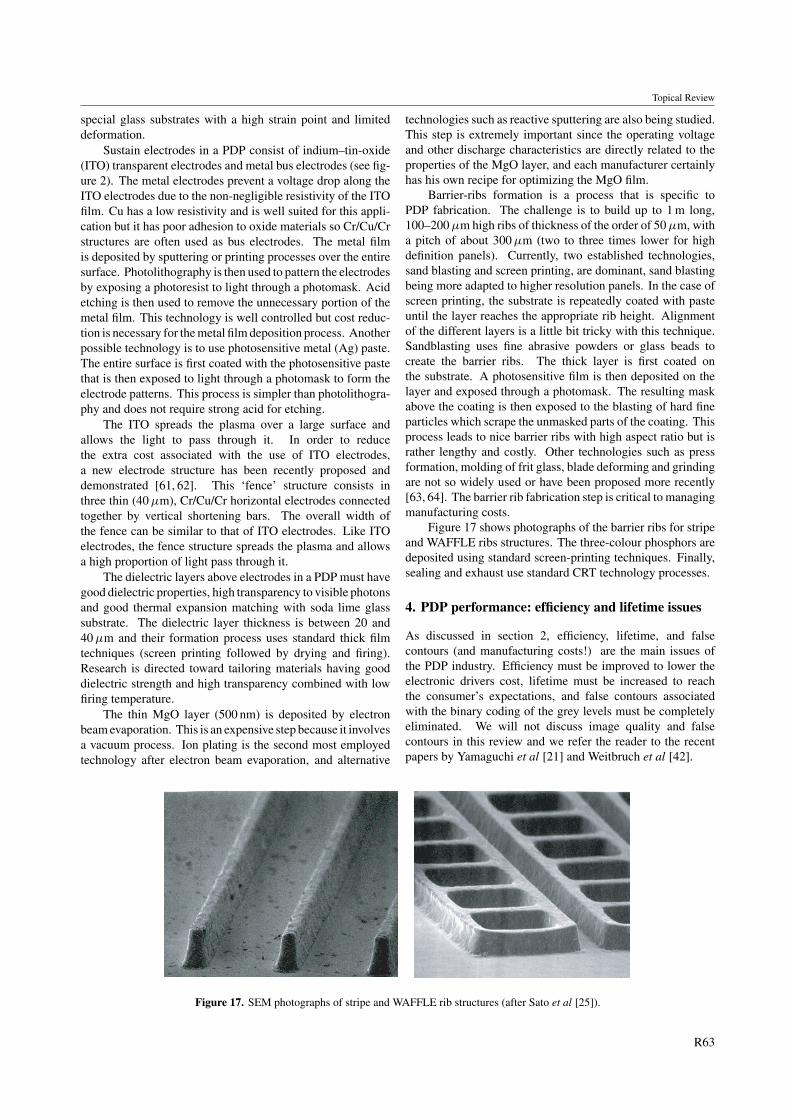
Figure 17. SEM photographs of stripe and WAFFLE rib structures (after Sato et al [25]).
technologies such as reactive sputtering are also being studied.This step is extremely important since the operating voltageand other discharge characteristics are directly related to theproperties of the MgO layer, and each manufacturer certainlyhas his own recipe for optimizing the MgO film.
Barrier-ribs formation is a process that is specific toPDP fabrication. The challenge is to build up to 1 m long,100–200 µm high ribs of thickness of the order of 50 µm, witha pitch of about 300 µm (two to three times lower for highdefinition panels). Currently, two established technologies,sand blasting and screen printing, are dominant, sand blastingbeing more adapted to higher resolution panels. In the case ofscreen printing, the substrate is repeatedly coated with pasteuntil the layer reaches the appropriate rib height. Alignmentof the different layers is a little bit tricky with this technique.Sandblasting uses fine abrasive powders or glass beads tocreate the barrier ribs. The thick layer is first coated onthe substrate. A photosensitive film is then deposited on thelayer and exposed through a photomask. The resulting maskabove the coating is then exposed to the blasting of hard fineparticles which scrape the unmasked parts of the coating. Thisprocess leads to nice barrier ribs with high aspect ratio but israther lengthy and costly. Other technologies such as pressformation, molding of frit glass, blade deforming and grindingare not so widely used or have been proposed more recently[63, 64]. The barrier rib fabrication step is critical to managingmanufacturing costs.
Figure 17 shows photographs of the barrier ribs for stripeand WAFFLE ribs structures. The three-colour phosphors aredeposited using standard screen-printing techniques. Finally,sealing and exhaust use standard CRT technology processes.
4. PDP performance: efficiency and lifetime issues
As discussed in section 2, efficiency, lifetime, and falsecontours (and manufacturing costs!) are the main issues ofthe PDP industry. Efficiency must be improved to lower theelectronic drivers cost, lifetime must be increased to reachthe consumer’s expectations, and false contours associatedwith the binary coding of the grey levels must be completelyeliminated. We will not discuss image quality and falsecontours in this review and we refer the reader to the recentpapers by Yamaguchi et al [21] and Weitbruch et al [42].
R63
Topical Review
The luminous efficacy of PDPs (ratio of visible radiation orluminous flux to power input) is low, of the order of 1–2 lm W−1
in currently produced PDPs. Laboratory prototypes showefficacy of 3 lm W−1, and the goal of the PDP manufacturers isto achieve 5 lm W−1. In this section we analyse the reasons forthis very low efficacy compared with what can be achieved influorescent lamps. We also discuss some of the lifetime issues.
4.1. General considerations about efficiency
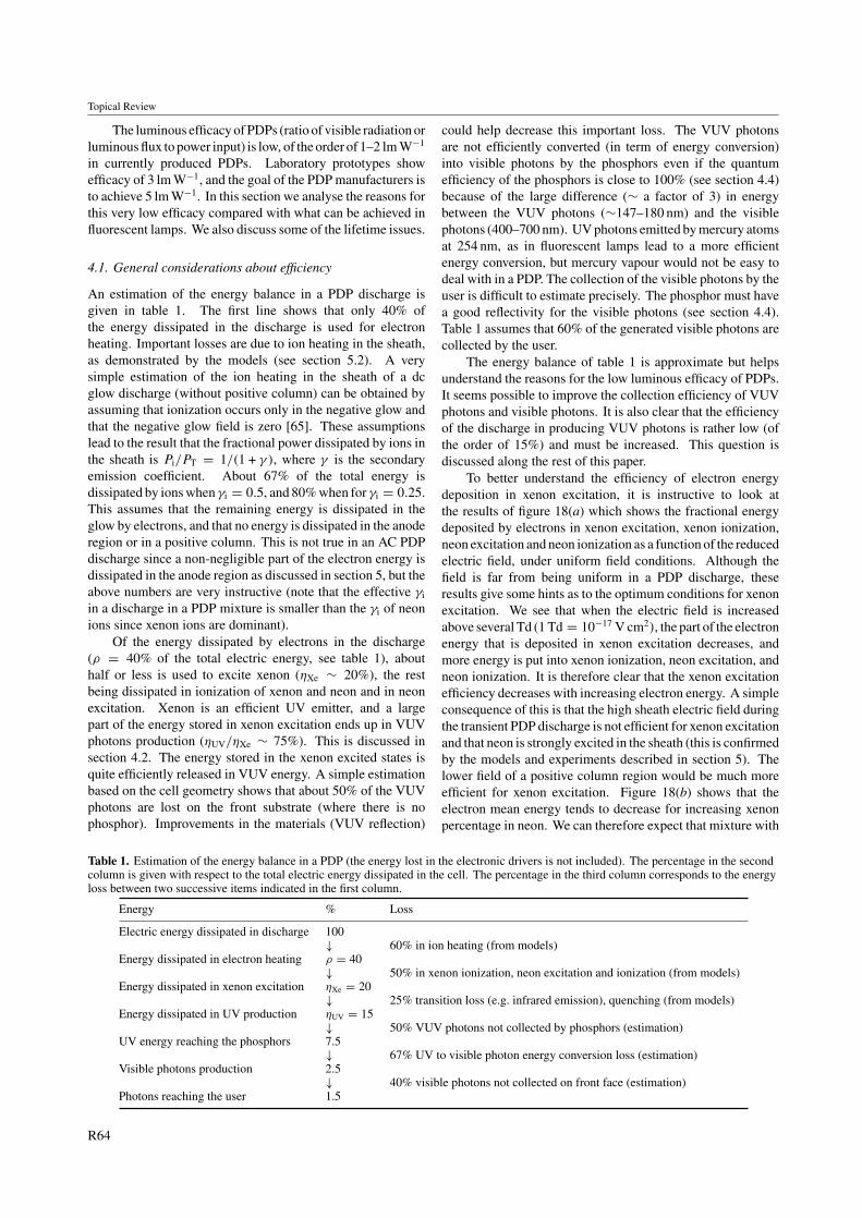
An estimation of the energy balance in a PDP discharge isgiven in table 1. The first line shows that only 40% ofthe energy dissipated in the discharge is used for electronheating. Important losses are due to ion heating in the sheath,as demonstrated by the models (see section 5.2). A verysimple estimation of the ion heating in the sheath of a dcglow discharge (without positive column) can be obtained byassuming that ionization occurs only in the negative glow andthat the negative glow field is zero [65]. These assumptionslead to the result that the fractional power dissipated by ions inthe sheath is Pi/PT = 1/(1 + γ ), where γ is the secondaryemission coefficient. About 67% of the total energy isdissipated by ions when γi = 0.5, and 80% when for γi = 0.25.This assumes that the remaining energy is dissipated in theglow by electrons, and that no energy is dissipated in the anoderegion or in a positive column. This is not true in an AC PDPdischarge since a non-negligible part of the electron energy isdissipated in the anode region as discussed in section 5, but theabove numbers are very instructive (note that the effective γi
in a discharge in a PDP mixture is smaller than the γi of neonions since xenon ions are dominant).
Of the energy dissipated by electrons in the discharge(ρ = 40% of the total electric energy, see table 1), abouthalf or less is used to excite xenon (ηXe ∼ 20%), the restbeing dissipated in ionization of xenon and neon and in neonexcitation. Xenon is an efficient UV emitter, and a largepart of the energy stored in xenon excitation ends up in VUVphotons production (ηUV/ηXe ∼ 75%). This is discussed insection 4.2. The energy stored in the xenon excited states isquite efficiently released in VUV energy. A simple estimationbased on the cell geometry shows that about 50% of the VUVphotons are lost on the front substrate (where there is nophosphor). Improvements in the materials (VUV reflection)
Table 1. Estimation of the energy balance in a PDP (the energy lost in the electronic drivers is not included). The percentage in the secondcolumn is given with respect to the total electric energy dissipated in the cell. The percentage in the third column corresponds to the energyloss between two successive items indicated in the first column.
Energy % Loss
Electric energy dissipated in discharge 100↓ 60% in ion heating (from models)
Energy dissipated in electron heating ρ = 40↓ 50% in xenon ionization, neon excitation and ionization (from models)
Energy dissipated in xenon excitation ηXe = 20↓ 25% transition loss (e.g. infrared emission), quenching (from models)
Energy dissipated in UV production ηUV = 15↓ 50% VUV photons not collected by phosphors (estimation)
UV energy reaching the phosphors 7.5↓ 67% UV to visible photon energy conversion loss (estimation)
Visible photons production 2.5↓ 40% visible photons not collected on front face (estimation)
Photons reaching the user 1.5
could help decrease this important loss. The VUV photonsare not efficiently converted (in term of energy conversion)into visible photons by the phosphors even if the quantumefficiency of the phosphors is close to 100% (see section 4.4)because of the large difference (∼ a factor of 3) in energybetween the VUV photons (∼147–180 nm) and the visiblephotons (400–700 nm). UV photons emitted by mercury atomsat 254 nm, as in fluorescent lamps lead to a more efficientenergy conversion, but mercury vapour would not be easy todeal with in a PDP. The collection of the visible photons by theuser is difficult to estimate precisely. The phosphor must havea good reflectivity for the visible photons (see section 4.4).Table 1 assumes that 60% of the generated visible photons arecollected by the user.
The energy balance of table 1 is approximate but helpsunderstand the reasons for the low luminous efficacy of PDPs.It seems possible to improve the collection efficiency of VUVphotons and visible photons. It is also clear that the efficiencyof the discharge in producing VUV photons is rather low (ofthe order of 15%) and must be increased. This question isdiscussed along the rest of this paper.
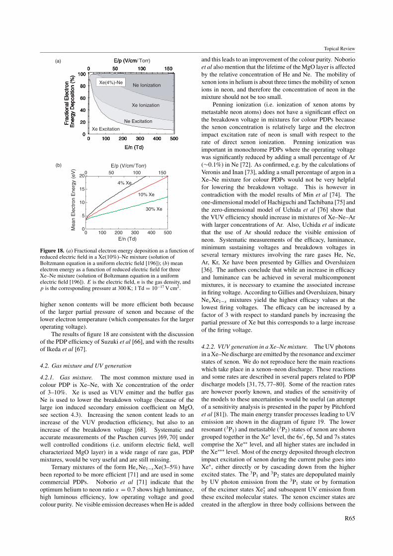
To better understand the efficiency of electron energydeposition in xenon excitation, it is instructive to look atthe results of figure 18(a) which shows the fractional energydeposited by electrons in xenon excitation, xenon ionization,neon excitation and neon ionization as a function of the reducedelectric field, under uniform field conditions. Although thefield is far from being uniform in a PDP discharge, theseresults give some hints as to the optimum conditions for xenonexcitation. We see that when the electric field is increasedabove several Td (1 Td = 10−17 V cm2), the part of the electronenergy that is deposited in xenon excitation decreases, andmore energy is put into xenon ionization, neon excitation, andneon ionization. It is therefore clear that the xenon excitationefficiency decreases with increasing electron energy. A simpleconsequence of this is that the high sheath electric field duringthe transient PDP discharge is not efficient for xenon excitationand that neon is strongly excited in the sheath (this is confirmedby the models and experiments described in section 5). Thelower field of a positive column region would be much moreefficient for xenon excitation. Figure 18(b) shows that theelectron mean energy tends to decrease for increasing xenonpercentage in neon. We can therefore expect that mixture with
R64
Topical Review
0 100 200 300 400 5000
20
40
60
80
100
Xe(4%)-Ne Ne Ionization
Xe Ionization
Ne Excitation
Xe Excitation
Fra
ctio
nal E
lect
ron
Ene
rgy
Dep
ositi
on(%
)
E/n (Td)
0 50 100 150
E/p (V/cm/ Torr)
(a)
0 100 200 300 400 5000
20
40
60
80
100
Xe(4%)-Ne Ne Ionization
Xe Ionization
Ne Excitation
Xe Excitation
Fra
ctio
nal E
lect
ron
Ene
rgy
Dep
ositi
on(%
)
E/n (Td)
0 50 100 150
E/p (V/cm
0 100 200 300 400 5000 100 200 300 400 5000
20
40
60
80
100
0
20
40
60
80
100
Xe(4%)-Ne Ne Ionization
Xe Ionization
Ne Excitation
Xe Excitation
Fra
ctio
nal E
lect
ron
Ene
rgy
Dep
ositi
on(%
)F
ract
iona
l Ele
ctro
n E
nerg
yD
epos
ition
(%)
E/n (Td)
0 50 100 1500 50 100 150
E/p (V/cm(a)
0 100 200 300 400 5000
5
10
15
20
E/p (V/cm/ Torr)
30% Xe
10% Xe
4% Xe
Mea
n E
lect
ron
Ene
rgy
(eV
)
E/n (Td)
0 50 100 150
(b)
Figure 18. (a) Fractional electron energy deposition as a function ofreduced electric field in a Xe(10%)–Ne mixture (solution ofBoltzmann equation in a uniform electric field [196]); (b) meanelectron energy as a function of reduced electric field for threeXe–Ne mixture (solution of Boltzmann equation in a uniformelectric field [196]). E is the electric field, n is the gas density, andp is the corresponding pressure at 300 K; 1 Td = 10−17 V cm2.
higher xenon contents will be more efficient both becauseof the larger partial pressure of xenon and because of thelower electron temperature (which compensates for the largeroperating voltage).
The results of figure 18 are consistent with the discussionof the PDP efficiency of Suzuki et al [66], and with the resultsof Ikeda et al [67].
4.2. Gas mixture and UV generation
4.2.1. Gas mixture. The most common mixture used incolour PDP is Xe–Ne, with Xe concentration of the orderof 3–10%. Xe is used as VUV emitter and the buffer gasNe is used to lower the breakdown voltage (because of thelarge ion induced secondary emission coefficient on MgO,see section 4.3). Increasing the xenon content leads to anincrease of the VUV production efficiency, but also to anincrease of the breakdown voltage [68]. Systematic andaccurate measurements of the Paschen curves [69, 70] underwell controlled conditions (i.e. uniform electric field, wellcharacterized MgO layer) in a wide range of rare gas, PDPmixtures, would be very useful and are still missing.
Ternary mixtures of the form HexNe1−xXe(3–5%) havebeen reported to be more efficient [71] and are used in somecommercial PDPs. Noborio et al [71] indicate that theoptimum helium to neon ratio x = 0.7 shows high luminance,high luminous efficiency, low operating voltage and goodcolour purity. Ne visible emission decreases when He is added
and this leads to an improvement of the colour purity. Noborioet al also mention that the lifetime of the MgO layer is affectedby the relative concentration of He and Ne. The mobility ofxenon ions in helium is about three times the mobility of xenonions in neon, and therefore the concentration of neon in themixture should not be too small.
Penning ionization (i.e. ionization of xenon atoms bymetastable neon atoms) does not have a significant effect onthe breakdown voltage in mixtures for colour PDPs becausethe xenon concentration is relatively large and the electronimpact excitation rate of neon is small with respect to therate of direct xenon ionization. Penning ionization wasimportant in monochrome PDPs where the operating voltagewas significantly reduced by adding a small percentage of Ar(∼0.1%) in Ne [72]. As confirmed, e.g. by the calculations ofVeronis and Inan [73], adding a small percentage of argon in aXe–Ne mixture for colour PDPs would not be very helpfulfor lowering the breakdown voltage. This is however incontradiction with the model results of Min et al [74]. Theone-dimensional model of Hachiguchi and Tachibana [75] andthe zero-dimensional model of Uchida et al [76] show thatthe VUV efficiency should increase in mixtures of Xe–Ne–Arwith larger concentrations of Ar. Also, Uchida et al indicatethat the use of Ar should reduce the visible emission ofneon. Systematic measurements of the efficacy, luminance,minimum sustaining voltages and breakdown voltages inseveral ternary mixtures involving the rare gases He, Ne,Ar, Kr, Xe have been presented by Gillies and Oversluizen[36]. The authors conclude that while an increase in efficacyand luminance can be achieved in several multicomponentmixtures, it is necessary to examine the associated increasein firing voltage. According to Gillies and Oversluizen, binaryNexXe1−x mixtures yield the highest efficacy values at thelowest firing voltages. The efficacy can be increased by afactor of 3 with respect to standard panels by increasing thepartial pressure of Xe but this corresponds to a large increaseof the firing voltage.
4.2.2. VUV generation in a Xe–Ne mixture. The UV photonsin a Xe–Ne discharge are emitted by the resonance and excimerstates of xenon. We do not reproduce here the main reactionswhich take place in a xenon–neon discharge. These reactionsand some rates are described in several papers related to PDPdischarge models [31, 75, 77–80]. Some of the reaction ratesare however poorly known, and studies of the sensitivity ofthe models to these uncertainties would be useful (an attemptof a sensitivity analysis is presented in the paper by Pitchfordet al [81]). The main energy transfer processes leading to UVemission are shown in the diagram of figure 19. The lowerresonant (3P1) and metastable (3P2) states of xenon are showngrouped together in the Xe∗ level, the 6s′, 6p, 5d and 7s statescomprise the Xe∗∗ level, and all higher states are included inthe Xe∗∗∗ level. Most of the energy deposited through electronimpact excitation of xenon during the current pulse goes intoXe∗, either directly or by cascading down from the higherexcited states. The 3P1 and 3P2 states are depopulated mainlyby UV photon emission from the 3P1 state or by formationof the excimer states Xe∗
2 and subsequent UV emission fromthese excited molecular states. The xenon excimer states arecreated in the afterglow in three body collisions between the
R65
Topical Review
+Ne, Xe
+e
+Ne, Xe
h
Xe+
Xe***
Xe**
Xe*
Xe Xe2
Xe2+
Xe2*
+e h
Atomic system Molecular system
+Ne, Xe
+e
+Ne, Xe
Xe+
Xe***
Xe**
Xe*
Xe Xe2Xe2
Xe2+Xe2Xe2+
Xe2*Xe2Xe2*
+e hν hν
Atomic system Molecular systemAtomic system Molecular system
Figure 19. Simplified energy level diagram for atomic andmolecular xenon, showing the important excitation and transitionprocesses in PDP conditions.
metastable or resonant states of atomic xenon with two raregas atoms:
Xe∗(3P1,3P2) + Xe + Xe (Ne) → Xe∗
2 + Xe (Ne).
The efficiency of the energy conversion from xenonexcited states to UV photon energy is quite high in theconditions of Xe–Ne PDP discharges. Energy losses in theconversion of atomic excited states to UV photons are dueto cascading from the Xe∗∗ and Xe∗∗∗ to the Xe∗ states(by collisions or radiative de-excitation) and to the energydifference between the metastable or resonance states andthe excimer states. The effective lifetime of the resonantstate is increased due to trapping (successive emission andre-absorption of the 147 nm photons) and this may lead toexcited state and hence VUV photon losses. When thedischarge power increases, excited species losses due tostepwise ionization [82, 83] may become important and leadto a saturation [84] of the VUV emission. However recentpapers show that under PDP conditions losses due to stepwiseionization of the excited states are not important [57, 85]. Thishad also been predicted by the models [31, 55, 86], in spiteof the uncertainties in the data related to stepwise processesand energy transfer within the atomic xenon system [81, 82].The consequence is that the discharge efficiency in producingVUV photons closely follows the efficiency in xenon excitation[73, 86]. Typically [31], if the xenon excitation efficiency is20%, the VUV photon production efficiency is about 15% (seetable 1).
Electron recombination with molecular ions (produced bythree body collisions) can be an indirect source of creation ofxenon resonant and metastable states:
Xe+ + Xe + Xe → Xe+2 + Xe,
Xe+2 + e → Xe∗∗ + Xe → Xe∗(3P1,
3P2) + Xe + hν.
Okigawa et al [87] and Tachibana et al [54] reportan increase in the metastable density (deduced from laserabsorption experiments) after the end of the current pulse,in the afterglow, which can be attributed to recombination.Infrared emission during the afterglow is also an indication of
the importance of electron recombination as a source of xenonresonant and metastable states. The time resolved emissionmeasurements of Dekker et al [88] show that about 5% and20% of the total infrared emission occur in the afterglow ina PDP cell in mixtures with 3.5% and 10% xenon in neon,respectively, for a sustain voltage of 180 V. At a higher voltageof 250 V, these percentages increase to about 40% and 60%,respectively. The calculations of Ganter et al indicate thatabout 10% of the total xenon excited state production is due toelectron recombination in the afterglow for a 10% xenon–neonmixture. We can conclude that there are large uncertainties inthe role of electron recombination on the overall xenon excitedstate production, but it seems that under standard conditionsof relatively low sustaining voltages recombination does notplay a major role.
4.3. MgO layer and secondary electron emission
The MgO layer is a key element of PDPs. This thin film(∼500 nm) protects the dielectric layer above the electrodesfrom sputtering while at the same time yielding a high-ioninduced secondary electron emission coefficient (γi) for Ne+.Because of its large secondary electron emission coefficientand good resistance to sputtering, the MgO layer plays anessential role in keeping the operating voltage relatively lowand in limiting the damages due to energetic ions. The MgOlayer is therefore important both for efficacy and lifetimeissues.
The combination of the emissive and protective propertiesmakes MgO quite unique and explains the fact that MgO,which was already used in the 1970s by Uchiike et al [89]and others [90, 91], is still used in the PDP industry in spiteof many attempts to find materials with better properties.The secondary electron emission coefficient of MgO underxenon ion bombardment is much lower than that of neonions. Therefore Ne plays an important role in lowering thebreakdown voltage in PDP gas mixtures, and this is one of thereasons why neon is used as a buffer gas in PDPs. Bachmannet al [92] recently showed that CVD diamond coatings can have(γi) values as large as MgO for neon ions and much larger thanMgO for xenon ions. Although the feasibility of using CVDdiamond coatings in PDPs has not yet been demonstrated, theseresults are encouraging and show that research for materialswith better properties than MgO should continue.
Note that although molecular ions are dominant in theafterglow plasma of a PDP discharge, they do not have timeto form in the sheath during the current pulse and the fluxof molecular ions to the surface is negligible with respect tothe flux of atomic ions [31]. We therefore discuss secondaryelectron emission and sputtering for atomic ions only.
Secondary electron emission is discussed in this sectionwhile section 4.4 deals with the aspects related to sputteringand lifetime.
4.3.1. MgO and other materials with large ion-inducedsecondary emission coefficient. MgO is not transparent toxenon UV photons, and several groups have been looking formaterials with better optical properties with respect to UVtransmission. A transparent film would allow coating of thephosphors on the front plate (the front plate phosphors would
R66
Topical Review
operate in transmission). Note that in the standard design ofAC PDPs (figure 2), UV photons hitting the MgO surface abovethe coplanar electrodes are lost. The corresponding loss in UVin efficiency is therefore close to 50%. Possible candidatesfor better transmission properties include MgF2 [93], Al2O3
and admixtures of MgO and Al2O3 [94]. Elsbergen et al [95]have measured secondary emission coefficients for MgO, TiO2
(good reflective properties for visible photons), mixtures ofMgO with Al2O3 or CaO. Some of the results of Elsbergenet al are shown in figure 20. Some nitrides (AlN) were alsostudied by Elsbergen et al because these materials could inprinciple exhibit negative electron affinity, but the authors didnot succeed in removing O-contaminations by annealing. Parket al [96–99] also reports measurements of secondary emissionyields for oxides and oxides mixtures such as Mg1−x−ySrx–Cay–O. They report better secondary emission than MgOfor some of these mixtures, but this is not confirmed by themeasurements of Elsbergen et al [95].
The secondary emission yield is also very sensitive tothe nature of the surface (amorphous, polycrystalline, singlecrystal, crystal orientation, etc). Elsbergen et al [100] reportthat the secondary coefficient for (111)-oriented MgO singlecrystals is substantially larger than for (110) and (100) (seefigure 21). They also show that the secondary emissioncoefficient reaches a constant value only after the surface has
100.01
0.1
1
50
Neon Ions on Oxides
MgO CaO-MgO Al
2O
3-MgO
Al2O
3
TiO2
Effe
ctiv
e γ
E/p (V/cm/ Torr)
Figure 20. Effective secondary emission coefficients deducedfrom breakdown measurements by the Lissajous method (see text)for different oxide mixtures in neon (after Elsbergenet al [95]).
0 10 20 30 40 50 60120
140
160
180
200
220
240
260MgO (100)
MgO (111)
MgO (110)
Bre
adow
n V
olta
ge (
V)
Burn Time (h)
Figure 21. Breakdown voltage of different MgO crystals, forpd = 7 Torr cm in Ne, as a function of burn time (i.e. duration ofexposure of the MgO substrate to a 30 kHz Ne plasma) (aftervan Elsbergen et al [100]).
been exposed to a plasma for a long enough time. The ‘burntime’ can be as large as several tens of hours as shown infigure 21. For MgO, the secondary coefficient increases duringthe burning time but the opposite is true for MgF2. Othermeasurements [101–103] made on single MgO crystals alsolead to conclusion that the (111) orientation of the MgO crystalhas the highest γi value.
4.3.2. Measurements of the secondary emission yield.Although most measurements show similar trends, there isa rather large dispersion in the γi measured by differentgroups. Two different approaches have been used, ion beammeasurements, and estimation of γi from breakdown voltagemeasurements (Paschen curves). Ion beam experimentsrequire sophisticated equipment and are not easy to performbecause (1) it is difficult to generate low energy ion beams(i.e. of the order of the energy of the ions hitting the MgOsurface in PDPs—the mean ion energy on the surface of aPDP cell is between 10 and 20 eV, and fast ions in the tailof the distribution may be up to about 100 eV at most), and(2) MgO is an insulator and the surface potential may varyduring the experiment due to charging effects. Ion beamtechniques have been used since the 1970s to characterize thesecondary electron emission of the protective layer in PDPs[89, 104]. In the early measurements the ion beam energy wastoo large to provide useful information for PDP conditions. Inmore recent experiments, measurements with lower ion beamenergy, down to 50 eV have been reported [101, 102, 105].In the energy range around 50 eV the measured γi is almostconstant or slowly increases with energy which is consistentwith Auger neutralization (i.e.γi depends on the internal energyof the incident ion, and not on its kinetic energy, see later).However the γi reported in several papers for (111) MgOcrystals [101, 102], and for polycrystalline MgO [105] arerather low, of the order of 0.05–0.1 for 50 eV neon ions, andabout twice larger at 200 eV. Other papers reporting ion beamexperiments give larger values of γi, ∼0.3 for 200 eV heliumions in Kim et al [96] and about 0.5 for 300 eV neon ions onMgO in Hirakawa et al [94]. The dispersion in the results istherefore very large and it is difficult to draw any quantitativeconclusion from these measurements (although comparativestudies for different materials or gases performed by the samegroup are useful).
The second approach is the classical use of breakdowncurves or swarm measurements (see the review paper by Phelpsand Petrovic [106] and references therein). In this approachone does not obtain the secondary emission coefficient dueto ion bombardment only, but an effective secondary electronemission γeff including the effects of ions, metastable atoms,and photons. The basic idea of using measured breakdowncurves or Paschen curves, is that along this curve, thebreakdown condition must be satisfied, i.e.:
exp[αd] = 1 +1
γeff,
where α is the ionization coefficient (supposed to be constantin the gas gap), d the gap length.
For this relation to be valid, the experiment must beperformed in uniform field conditions, and corrections mustbe included for possible non-local effects when the gap length
R67
Topical Review
is not much larger than the electron energy relaxation length[106]. Knowing the ionization coefficient α and its dependenceon electric field E/n (electric field strength over gas density),one can deduce γeff as a function of E/n. The situation ismore complicated when the surface is an insulator, since thegas gap voltage decreases during the pre-breakdown phase dueto accumulation of charges on the dielectric surface. A naturalway to overcome this problem is to use AC voltage pulsesto characterize breakdown. Sahni and Lanza [107] point outthat the maximum sustaining voltage is the closest AC panelequivalent to the breakdown voltage. A way to deduceγeff fromAC breakdown measurements is therefore to use a dischargecell similar to a matrix PDP cell, with dielectric layers coveredwith MgO, but with electrode dimensions sufficiently largerthan the distance between electrodes to ensure field uniformity.An AC rectangular voltage is applied between the electrodesand slowly increased until cell ignition is achieved. It is ofcourse important that all remaining charges on the dielectricsurface be erased before a new measurement starts which isnot the case when the measurements are not performed underAC conditions [108]. The rise time of the AC voltage pulsemust be as short as possible so that electron multiplicationoccurs mainly during the constant voltage step. This methodwas used in the early studies of PDPs [107, 109, 110]. Thequestion of the influence of the applied frequency (30 kHz inthe paper of Aboelfotoh and Lorenzen [109]) of the AC voltageis not discussed, and it is not clear in what frequency rangethe breakdown results are independent of frequency. Morerecently, breakdown measurements based on the Lissajousmethod have been reported [95, 100, 111]. In this method asinusoidal voltage is applied to the discharge cell in series witha known capacitor. The voltage on the capacitor at each instantis plotted as a function of the applied voltage. This gives ahysteresis curve from which one can deduce the gas gap voltageand thus the breakdown voltage. This technique is valid whenthe frequency of the applied sinusoidal voltage is small enoughso that the discharge never reaches a glow regime but ratherstays in the Townsend regime. Similar measurements couldalso be performed with a ramp AC voltage with a rise time smallenough to prevent the discharge transition from the Townsendto the glow regime. In these conditions, as soon as the voltageacross the gap reaches the breakdown voltage, the Townsendcurrent charges the dielectric surface in such a way that thegas gap voltage is kept constant and equal to the breakdownvoltage. This is reminiscent of Weber’s concept of using aramp voltage for priming (see section 3.3 and Weber [41]).This method seems very attractive but the dependence of theresults on the applied frequency (especially for pd productslarger than 30 Torr cm [111]) is not yet understood and thereis a need for a theoretical or modelling clarification of thistechnique.
The values of the effective secondary electron emissionγeff shown in figure 20 have been deduced from Lissajousbreakdown voltage measurements by Elsbergen et al [111] inpure neon and for different oxides.
It must be stressed that the methods of estimation ofthe secondary electron emission based on breakdown curvesgive an effective coefficient which includes the effect of ionbombardment, but also the effect of metastable and photonimpact. Each of these phenomena may be dominant in different
parts of the breakdown curve. For example it is known thatthe contribution of the secondary emission coefficient dueto photons is more important for lower E/n or E/p values(i.e. larger pd on the breakdown curve). It must also bekept in mind that under some conditions it is possible thatthe breakdown voltage does not depend on the pd productonly, but depends separately on pressure and gap length. Thishas been observed by Sahni and Lanza [112] in the contextof monochrome AC PDP (Ne + 0.1%Ar mixture) and was(tentatively) attributed to the fact that atomic and molecularneon ions have different secondary emission coefficients, andthat the ratio of molecular to atomic ion flux to the cathodesurface increases with pressure.
From the above discussion, we can conclude that thereis still a large uncertainty in the γi and γeff deduced fromion beam and breakdown experiments, respectively. Thedifferent experimental results are in agreement on the factthat the secondary emission coefficients decrease for raregases in this order: He, Ne, Ar, Kr, Xe, which is consistentwith the theory (see later). Also the ion beam experimentsas well as the breakdown measurements show that in thecase of MgO crystal, the (111) orientation gives the largestγi. As mentioned above several authors have mentioned thatthe measured γ reaches a constant value after an exposureto ion bombardment for a long enough duration (more than10 h for MgO single crystals as reported by Elsbergen et al[100], see figure 21). Annealing of the MgO surface is alsoa necessary process and the typical preparation of MgO forPDPs involves an annealing process at a temperature of theorder of 400˚C or more (see, e.g. Delplancke-Ogletree et al[113] for a study of thermal annealing and effect of exposureto water vapour on the surface structure of single crystal MgOsubstrate). There are two reaction routes related to waterchemisorption on MgO: the formation of hydroxide and ofcarbonate [97, 114]. Delplancke-Ogletree et al [113] reportthat exposure to humidity modifies the morphology of MgOsubstrates by the formation of Mg(OH)2 clusters and theirresults indicate that an MgO crystal cannot be exposed for morethan 10 h at 40% or 1.5 h at 80% humidity without undergoingmajor morphological and chemical transformation.
4.3.3. Theoretical determination of the secondary emissioncoefficient. The theory of electron emission due to Augerejection of electrons from metal or semiconductor surfaces issummarized in two classical papers by Hagstrum [115, 116].Secondary emission by low energy ions depends mainly onthe ions potential energy and not on their kinetic energy.In the case of insulating surfaces, the theory shows thatthe secondary emission yield due to Auger emission is acombination of (1) Auger neutralization, and (2) resonanceneutralization followed by Auger de-excitation. In the secondcase the ion is first transformed into an excited atom whenapproaching the surface. Even if the probability of theresonance neutralization cannot be easily calculated, it is clearthat the total secondary emission coefficient is in betweenthe coefficients corresponding to Auger neutralization andAuger de-excitation. Unlike for metal surfaces, the Augerneutralization secondary electron emission yield does notdepend on the surface work function but on the sum of theband gap Eg and electron affinity χ of the insulator surface,
R68
Topical Review
Table 2. Calculated values of the secondary emission coefficient (γ N through Auger neutralization, and γ D through resonance neutralizationfollowed by Auger de-excitation) for MgO and BaO assuming a flat band. After Motoyama et al [117]. In the case of rare gases and MgO orBaO, γi = γ N, and γm = γ D where γi and γm are the secondary electron emissions due to ion and metastable impacts, respectively [117].
Gas He Ne Ar Kr Xe
Ei, Em (eV) 24.58 19.81 21.56 16.61 15.76 11.55 14.00 9.91 12.13 8.31
and on the ion internal energy Ei. More precisely, the emissionof electrons by the Auger neutralization process is non-zerowhen the parameter G = Ei − 2(Eg + χ) is positive, andincreases for increasing G. Therefore, for a given surface, γi
will increase with increasing Ei, and Xe, Kr, Ar, Ne, He inthis order will have increasing γi. Note that G is negative forKr and Xe ions on MgO (if we take, as in Aboelfotoh andLorenzen [109], a band gap and electron affinity of 6.8 eVand 0.85 eV, respectively) and thus no secondary emission dueto Auger neutralization would be expected for Kr and Xe.However the quantity H = Eexc − (Eg + χ) where Eex isthe excitation energy, is positive for all the noble gases andsecondary emission due to Auger de-excitation should be non-zero even for xenon and krypton.
Aboelfotoh and Lorenzen [109], Motoyama et al [117],and Yoon et al [118] have used the Hagstrum theory to calculatethe ion-induced secondary electron emission yield. The valuesobtained by Motoyama et al [117] for noble gases on MgOand BaO, for the Auger neutralization and Auger de-excitationprocesses are shown in table 2. The calculations of Yoon et al[118] give γi values which are slightly larger than those ofMotoyama et al probably because of different assumptions onthe electron escape probability involved in the Auger emissionprocess.
From the results of table 2 we see that the theoreticalsecondary emission coefficient due to ion impact γi is 0.29for neon ions on MgO and is 0 for xenon ions. The theoreticalsecondary emission coefficient due to metastable atom impactγm is 0.38 for neon and 0.11 for xenon.
Note finally that in a discharge, some of the emittedelectrons are backscattered at the cathode. The proportionof backscattered electrons is large for low electric fields andtends to zero for sufficiently large fields [106, 119, 120]. Theabove theoretical values or ion beam measured values of thesecondary electron emission coefficient should therefore becorrected to account for backscattered electrons when used influid discharge models.
We can conclude from this section that the theoreticalvalue of the secondary emission coefficient on MgO due toneon ions is generally larger than the value measured in ionbeam experiments (0.1–0.3) but lower than values deducedfrom Paschen measurements (>0.3). The theoretical value of0 for xenon ions on MgO is quite remarkable since xenon ionsare dominant in a PDP discharge and shows that the actualγi of xenon ions will strongly depend on the preparation ofthe MgO surface and on the nature of impurities or dopantsincluded in the layers. The large dispersion of the measuredresults and the strong dependence of the coefficients onthe surface preparation make difficult detailed comparisonsbetween experiments and models of PDP cells.
4.4. MgO sputtering
Energetic ions hitting a surface can lead to the ejection of atomsfrom the surface. The fast ions also transmit their energy toneutral atoms in the sheath through charge exchange collisions,and the resulting fast neutral atoms can also damage the surface(see McClure [121], Abril et al [122], and the calculationsin Revel et al [123]). Although MgO is quite resistant tosputtering, aging due to sputtering cannot be avoided. Thesputtering of MgO may also lead to a contamination of thephosphors (by re-deposition).
In order to estimate the erosion rate or the lifetime ofthe MgO surface, it is necessary to calculate the energydistribution of ions and neutral atoms hitting the surface abovecathode. Several calculations of the ion distribution functionat the surface have been reported recently [124–129] (see alsoCapdeville et al [130] for sputtering calculations in Xe–Ne andXe–Ar mixtures in DC discharges).
The calculated energy distribution functions depend ofcourse on the ion–neutral and neutral–neutral cross-sections,and it is important to use accurate cross-sections. Chargeexchange collisions are especially important in limiting theion energy in the sheath. The cross-sections in Shin et al [124]are not discussed (only elastic collisions are mentioned in thispaper). Hagelaar et al [125] calculated the energy distributionof ions and fast neutral atoms using a Monte Carlo simulationat the moment of maximum ion flux (predicted by a two-dimensional fluid model of a PDP discharge). They proposeanalytical expressions of the ion distribution that fit well theirnumerical results. Piscitelli et al [127–129] calculated theion and neutral atoms energy flux distribution with a transientMonte Carlo simulation using the space and time electricfield and ionization rates generated by a one-dimensional fluidmodel. Yoon et al [126] used the analytical expressions ofHagelaar et al [125] combined with discharge data from atwo-dimensional fluid model. From these distributions, andusing the sputtering yield obtained with TRIM (a Monte Carlosimulator of the ion–surface interaction [131]), they deduce thelifetime of the MgO layer. All the models agree with the factthat the high energy tail of the xenon ion flux distribution ismore populated at lower Xe concentrations while the oppositeis true for neon ions, as seen in figure 22. This is because thenumber of charge exchange collisions between Xe+ and Xeatoms decrease for decreasing Xe percentage while the numberof charge exchange collisions between Ne+ and Ne increases.The high energy tail of the ion flux distributions is much lesspopulated in the results of Shin et al [124] and Hagelaar et al[125] than in Piscitelli et al [127–129] and Yoon et al [126]probably because different cross-sections were used in thesepapers.
R69
Topical Review
0 50 100 150 20010
9
1010
1011
1012
1013
1014
1015
30%
20%
10%
5%
XenonE
ne
rgy d
istr
ibu
tio
n (
eV
-1m
-2)
Energy (eV)
0 50 100 15010
9
1010
1011
1012
1013
1014
1015
10%
30%
5%
Neon
En
erg
y d
istr
ibu
tio
n (
eV
-1m
-2)
Energy (eV)
Figure 22. Time integrated flux energy distribution of the ions and fast neutral atoms on the MgO surface above cathode calculated with aMonte Carlo simulation using the space and time electric field and ionization rate from a one-dimensional fluid model (mid-margin, gas gap100 µm, 500 Torr) (after Piscitelli et al [129]). The ion–neutral and neutral–neutral cross-sections used in the simulations are from Phelpset al [197].
Even if the ion flux energy distribution can be accuratelycalculated (if the cross-sections are accurate), it is difficultto estimate the erosion rate (and lifetime) of the MgO layerbecause it strongly depends on the sputtering yield of thesurface near the energy threshold. The sputtering yield canbe measured in beam experiments, but measurements at lowion energy are very difficult [132]. The sputtering yieldas a function of ion incident energy can be estimated fromMonte Carlo simulations of the ion–surface interaction but theuncertainties are large. In the case of Xe–Ne mixtures, thecalculated ion energy distributions show that Xe+ ions are lessenergetic for larger xenon partial pressure but Ne+ ions aremore energetic. One can therefore expect that xenon ions cancause more damages to the surface at low xenon concentrationswhile neon ions can cause more damages at higher xenonconcentrations (the sputtering threshold of neon ions seemslower that that of neon ions [126], so that even though the neonion current decreases when increasing the xenon concentration,the contribution of neon ions to sputtering may increase). It istherefore possible that the erosion rate of the MgO surface has aminimum (optimum lifetime) for a given xenon concentrationbut this needs to be confirmed [129].
4.5. Phosphors
A summary of the demands and achieved performance of PDPphosphors can be found in the recent paper by Bechtel et al[133]. In a PDP, phosphors are used to convert VUV lightfrom xenon, into visible light. Phosphor materials must havea high quantum efficiency and low reflectivity for the VUV,and must be highly reflective for visible light. The quantumefficiency at a given wavelength is defined as the ratio of thenumber of emitted visible quanta to the number of absorbedUV quanta. State of the art PDP phosphors have achievedquantum efficiency in the range from 80% to 95% for xenonUV photons between 147 and 190 nm [133]. The phosphormaterials used in PDP applications are BaMgAl10O17 : Eu2+
(BAM) for blue emission, Zn2SiO4 : Mn2+ for green emission,and (Y, Gd)BO3 : Eu3+ and Y2O3 : Eu3+ for red emission. Theblue and green phosphors have light output (ratio of the numberof emitted visible quanta to the number of incident UV quanta,i.e. conversion efficiency including the effect of reflection)
above 80% in the xenon VUV range. The red phosphors are alittle bit less efficient (the light output of (Y, Gd)BO3 : Eu3+ isclose to 80% at 147 nm and about 60% around 173 nm while thelight output of Y2O3 : Eu3+ is of the order of 60% at 147 nm,and closer to 80 around 173 nm). The quantum efficiency,reflectivity and light output of these phosphor materials areplotted as a function of wavelength in Bechtel et al [133].
As reported by Bechtel et al, the blue emitting BAMphosphor is more vulnerable to panel processing anddegradation under panel operation. The quantum efficiencyand light output of the BAM phosphor decrease by a factor of2 for 147 nm photons for an annealing temperature of 1000 K.
Finally, note that the overall efficiency of the photonconversion process (including scattering and absorption of theemitted photons) depends on the size of the phosphor particles.Simulations of the photon conversion process in a PDP cell[133] based on Mie scattering theory show that for a givenphosphor layer thickness between 20 and 30 µm, the optimumdiameter of the phosphor particles is 1–2 µm.
5. Modelling and diagnostics
Sophisticated modelling and optical diagnostic tools have beendeveloped in the last ten years to study and optimize thedischarge plasma in PDPs. In this section we present a non-exhaustive overview of the recent developments of modellingand diagnostic tools.
5.1. PDP models
The first detailed PDP model has been developed by Sahniand Lanza [72] at IBM, for a Ne–Ar (typically 0.1% Arin Ne), monochrome PDP. The model was one-dimensionaland based on fluid equations for electrons, ions, and excitedatoms, coupled with Poisson’s equation for the electric field.Sahni et al demonstrated the capability of such models tosuccessfully simulate the fundamental processes occurring in aPDP cell, from the first principles of gaseous electronics. Theyshowed that the available data (transport coefficients, reactionrates) in Ne–Ar mixtures allowed a detailed understandingof the discharge and relatively accurate predictions of the
R70
Topical Review
current pulse and voltage-transfer curves. They also showedthat the results are very sensitive to the secondary emissioncoefficient of neon and argon ions on the MgO surface[107, 134]. Meunier et al [31] developed a similar one-dimensional model, based on the local field approximation, tostudy a PDP discharge in a matrix electrode configuration, inXe–Ne mixtures. A detailed energy balance deduced from thismodel showed that a large part of the electric energy consumedin the discharge (more than 60% in standard conditions) isdissipated by ions in the sheath. The results showed that about10% of the electric energy dissipated in the discharge was usedto produce UV photons in a Xe(10%)–Ne matrix discharge(100 µm gas gap, 560 Torr, 142 V sustaining voltage). Themodel also showed that the UV production efficiency canincrease with increasing Xe content but that, as well knownfrom experiments (see figure 7), the operating voltage is largerfor larger Xe concentrations.
Several papers on one-dimensional models of colour PDPhave been published since 1995 [75, 135–139]. After thefirst two-dimensional models of Uchiike et al [140, 141], anincreasing number of papers on two-dimensional models haveappeared [32, 38, 55, 77, 78, 142–149]. More recently, three-dimensional models of PDP discharges have been developed[150–153]. All the models cited above are fluid models, i.e. thecharged particle transport properties are described by averagevalues. A few, more detailed, particle-in-cell Monte Carlo(PIC-MCC) simulations of PDP cells have also been developedrecently [154, 155]. These models are time consuming andnot well adapted to the relative large collisionality of PDPdischarge nor to systematic parametric studies. They mayhowever be very useful to help understanding some detailedproperties of electron and ion transport in PDP cells.
Using a two-dimensional fluid model, Boeuf et al[32, 38, 142, 143] showed that a non-negligible part of thexenon excitation in a PDP discharge occurs in the anode region,during the spreading of the plasma along the dielectric surfaceabove anode. This feature was later confirmed in opticalemission spectroscopy and CCD imaging experiments (seesection 5.2), and by all the two-dimensional models. Two-dimensional simulations of the basic operation (writing andsustaining) of a PDP cell in coplanar electrode configurationswere described by Boeuf et al [68], Punset et al [38], and Raufand Kusher [77, 147]. The ability of the models to simulatethe writing and sustaining pulses was demonstrated in thesepapers.
Figure 23 illustrates the properties of the writing andsustaining discharges as deduced from two-dimensionalmodels. During the writing pulse, breakdown occurs betweenone of the coplanar electrodes (temporary cathode) and theaddress electrode. We see the spreading of the plasmaabove anode and the sheath formation above cathode. Xenonexcitation occurs both on the anode and cathode side. Thememory charges deposited on the dielectric surfaces duringwriting allow breakdown between the coplanar electrodesduring the sustaining pulse. The glow above the cathodeindicates the sheath formation and spreading along theelectrode. The plasma spreading along the anode is alsoaccompanied by significant xenon excitation. This excitationis due to the electric field parallel to the surface, induced by theprogressive charging of the dielectric surface. Experimental
0 10.5
4 W.mm-3 46 W.mm-3 22 W.mm-3
-30
30
60 11
-30
3060
200 ns 214 ns
-30
130
60
222 ns
0
-200
+ 8
0
-120 -60
3060 30
0 -30
-30
-120
90
60
60
0 -30
-60
-30
150
-120
-30
-30
-60
600
3420 ns 3440 ns 3458 ns
4.5 W.mm-3 42 W.mm-3 25 W.mm-3
0
0
-180
Figure 23. Spatial distribution of power dissipated in xenonexcitation (colour) and electric potential (contours) during thewriting pulse (top) and the first sustaining pulse (bottom) of a PDPdischarge cell (after Punset et al [32]). The gas mixture is Xe–Ne(5–95%) at 500 Torr; the cell dimensions are 600 µm × 160 µm(periodic boundary conditions). The applied voltages are shown infigure 5.
results (see section 5.2) confirm this interpretation but show amore complex, striated shape of the emission above the anode.
Rauf and Kushner compared results from a local fieldmodel, with results from a hybrid model where a MonteCarlo simulation was used to describe the fast electrons. Inagreement with Boeuf et al [68], Rauf and Kushner [77]found that the local field approximation did not significantlyaffect the minimum sustaining voltage, the total currentfluence during the discharge, or the accumulated charges onthe dielectric surfaces, but that some characteristics such asthe discharge initiation time predicted by the local field andMonte Carlo models were different. As in the matrix electrodeconfiguration, the two-dimensional simulations in a coplanarcell showed that an important part of the xenon excitationoccurs above the anode. Veronis and Inan [148] also reportsome differences between results from fluid models using thelocal field approximation or a local energy approximation.
The calculated data pulse voltage margin in Punset et al[38] is in good agreement with the experimental values andthese results showed that the two-dimensional model can be avery useful tool for cell optimization. The obvious limitationof the two-dimensional-model is that the cell is supposed to beinfinite in the direction perpendicular to the simulation domain.This implies that the width of the address electrode is infinitein the simulation (i.e. the address electrode is not a strip buta plane). The capacitance between the address electrode andthe plasma is therefore overestimated by the two-dimensionalmodels, and this has some consequences on the simulatedsurface charge distribution in the cell, as described by Punsetet al [38].
R71
Topical Review
Hagelaar et al [156, 157] developed efficient and accuratenumerical algorithms for PDP fluid models. They discuss[156] the appropriate boundary conditions that must be usedin fluid models where the charged particle flux has a drift-diffusion form. An implicit treatment of the energy equationsource term that can considerably speed up the simulation isdescribed by Hagelaar et al [157]. More recently, Veronis andInan [148] presented a similar two-dimensional fluid model ofa coplanar discharge and discussed the effect of introducingfloating electrodes in the dielectric layers.
One property of the plasma in a PDP cell that is notwell described by fluid models is the presence of striationsabove anode. These striations are clearly seen in opticalemission spectroscopy or imaging experiments (see section .2).PIC-MCC models however seem to predict these striations[155,158] (although striations are not mentioned in the paperby Ikeda et al [154]), but a clear physical understanding ofthe mechanisms leading to the formation of striations is stillmissing.
The models are also very useful because of their abilityto give a quantitative estimation of the energy balance in thedischarge. One of the important and clear conclusions of all themodels cited above is that in typical PDP discharge conditions,a large part of the electrical energy is dissipated in ion heatingin the sheaths. The energy is subsequently dissipated throughcollisions with neutral atoms or when the ion hits the surface.Meunier et al [31, 68], Hagelaar et al [55] and other authorsdeduce from their models that more than 60–70% of the inputelectric energy is dissipated in ion heating. The remaining30–40% is dissipated into electron heating. The electronsrelease mainly their energy in xenon or neon excitation andionization. Roughly speaking about one-half of the electronenergy can be dissipated into xenon excitation, the rest beingdissipated mainly in xenon and neon ionization and in neonexcitation. Therefore about 20% of the total energy dissipatedin the discharge can be dissipated in xenon excitation. A largepart of this energy (about 80% [31]) is then released into VUVphoton energy through cascading and three-body collisionsleading to resonant or excimer photon emission.
The two-dimensional model results of Hagelaar et al[55] displayed in figure 24 show that between 10% and16% of the total electric energy dissipated in VUV photonenergy in a coplanar discharge under standard conditions(5% Xe, 450 Torr). The efficiency in electron heating (i.e.the part of the total electric energy dissipated in electronheating) is also presented in this figure. The calculationsshow that the discharge efficiency in producing VUV photons(ηUV in figure 24) increases as a function of voltage andsaturates at about 300 V for a sustaining voltage frequencyof 50 kHz. The electron heating efficiency (ρ in figure 24)increases proportionally to ηUV, meaning that the part ofthe electron energy which is used to produce VUV photonsdoes not significantly change with voltage (ηUV, the VUVdischarge efficiency, is the product of ρ, the electron heatingefficiency, and the efficiency of the conversion of electronenergy into VUV photon energy). Hagelaar et al [55] reportthat this increase of efficiency with voltage is consistent withexperiments. The simulations of Rauf and Kushner [147]though do not show an increase of efficiency with voltage.It would certainly be very useful to perform benchmark
200 250 300 350
10
12
14
16
18
Par
tial e
ffici
ency
(%
)
Effi
cien
cy (
%)
Vs (V)
25
30
35
40
45
ρ
ρ
η
ηUV
250 kHz
50 kHz
Figure 24. Calculated VUV discharge efficiency as a function ofsustaining voltage in a coplanar cell, in a 450 Torr, Xe(5%)–Nemixture, and for two values of the sustaining frequency. ηUV is thedischarge efficiency in producing VUV photons (i.e. the ratio of thetotal energy of the emitted VUV photons divided by the total electricenergy dissipated during one pulse). ρ is the percentage of the totalenergy dissipated in electron heating (the rest, i.e. between 55% and70% on this graph, being dissipated in ion heating) (after Hagelaaret al [55]).
calculations to compare the results from different models inorder to identify the real cause for discrepancies (there arelarge uncertainties in some parameters of the simulation, suchas secondary electron emission, ion mobilities in mixtures, orsome reaction rates). Another interesting finding of Hagelaaret al (see figure 24) is that the efficiency drops if the sustainingvoltage frequency is too large. In the 50 kHz case or for lowerfrequencies the successive pulses are practically independentof each other. For these frequencies only the delay time tobreakdown depends on the volume charges (or excited species)remaining from the previous pulse. If the frequency is overa critical value, the delay time may become shorter than therise time of the voltage pulse. In this case breakdown actuallyoccurs during the voltage rise time and the discharge efficiencydecreases.
As a general rule the different two-dimensional modelsshow that for a given gas mixture and pressure, there isno spectacular increase of the discharge efficiency whenthe cell parameters (coplanar electrode gap length, electrodewidth, dielectric permittivity) are slightly changed around thestandard values. The models agree that the discharge efficiencyincreases with xenon concentration and with pressure, but atthe expense of the minimum sustaining voltage, which alsoincreases with Xe concentration and pressure (the operatingvoltage must be kept as low as possible to keep reasonableelectronic drivers costs).
The models can also predict the fraction of VUV photonsreaching the phosphors that are emitted by the resonant atomicstate of xenon or by the excimer state. The predictions ofthe two-dimensional model of Hagelaar et al are shown infigure 25. We see that about 50% of the VUV photons areemitted by the resonant atomic state for a Xe(5%)–Ne mixture.This percentage drops to about 30% for a Xe(15%)–Nemixture. This is due to the increase of radiation trapping withincreasing xenon partial pressure. The trapping of resonantphotons leads to an increase of the production rate of excimerphotons through three-body collisions.
R72
Topical Review
0 5 10 15 200.2
0.3
0.4
0.5
0.6
0.7
0.8
0.9
1.0
experiment
calculation
reso
nanc
e/to
tal U
V e
nerg
y
xenon content (%)
Figure 25. Calculated fraction of the total VUV energycorresponding to resonant photons (147 nm), as a function of xenonpercentage (225 V, 450 Torr, 250 kHz) (after Hagelaar et al [55]).
The results of figure 25 were obtained assuming thatthe resonance radiation transport can be described with theclassical theory of Holstein [159], i.e. using an effectivetime (or a trapping factor) to account for radiation trapping.A more detailed Monte Carlo simulation of the resonanceradiation transport by Hagelaar et al [160] showed that thisapproach is good enough and that the trapping factor estimatedfrom Holstein’s theory was in good agreement with the valuededuced from the Monte Carlo simulation. The more detailedMonte Carlo approach can also predict the spectrum of theresonant photons leaving the discharge, which can be measuredexperimentally. As expected, this spectrum exhibits largerwings than a Lorentz profile, and a weaker centre. Thesimulations of Hagelaar et al are in excellent agreement withthe measurements [160]. Similar results have also beenpresented by van Straaten and Kushner [161], Tamida et al[162], and Lee et al [163].
5.2. Optical spectroscopy and imaging
Detailed optical diagnostics of the plasma in PDP cellshave been performed in the last 10 years. These includehigh resolution, time resolved, optical emission spectroscopy[164], laser absorption techniques [54, 87, 165], imagingusing intensified charge-coupled devices (CCD) in theVUV [166–169] and infrared and visible wavelength range[56, 170–173], and, more recently, laser induced fluorescencemeasurements of the electric field [174] and laser Thomsonscattering measurements of the electron temperature anddensity [175, 176].
In their optical emission spectroscopy measurements,Yoshioka et al [164] achieved spatial resolution of 10 µm andtemporal resolution of 10 ns. They measured emission linesof atomic He (706.5 nm), Ne (640.2 nm), Xe (823.1, 828.0,467.1 nm), and ionic Xe (484.4 nm) in Xe–Ne–He mixturestypical of PDPs. The cell dimensions were 1 mm × 0.3 mm ×0.12 mm, the coplanar electrode gap was 100 µm and theelectrode width 400 µm. The pressure was varied between 100and 600 Torr, and the xenon concentration was between 1% and20%. The cell was driven with rectangular voltage pulses at10 kHz, in conditions similar to those of a real PDP cell.
Figure 26 shows the distribution of Xe (823.1 nm) and Ne(640.2 nm) above the electrodes (from a top view of the cell,
0 500AnodeCathode
670 ns
710 ns
750 ns
790 ns
850 ns
Xe (823.1 nm)
Ne (640.2 nm)
0.
0.6
0.
0.6
0.
0.6
0.
0.6
0.
0.6
0 500AnodeCathode
670 ns
710 ns
750 ns
790 ns
850 ns
Xe (823.1 nm)
Ne (640.2 nm)
0 500–500 AnodeCathode
670 ns
710 ns
750 ns
790 ns
850 ns
Xe (823.1 nm)
Ne (640.2 nm)
0.
0.6
0.
0.6
0.
0.6
0.
0.6
0.
0.6
0.
0.6
0.
0.6
0.
0.6
0.
0.6
0.
0.6
Position (µm)
Figure 26. Spatio-temporal emission profiles above the coplanarelectrode in a Xe(4%)–Ne mixture at 400 Torr. Neon visibleemission (- - - -) mainly occurs above cathode while xenon emission(——) takes place over both cathode and anode. Standing striationsare observed above anode (after Yoshioka et al [164]).
along a line in the middle of the coplanar electrodes) at differenttimes of a discharge pulse in the sustaining regime (400 Torr,Xe(4%)–Ne). We see that light emission first occurs abovethe anode edge, close to the coplanar gap. After some time anemission peak appears above cathode. This peak correspondsto the negative glow light and moves along the cathode surfacesas the cathode sheath spreads on the dielectric surface abovecathode. In the meantime the emission peaks also grow abovethe anode edge. Three other peaks later appear during theplasma spreading above anode. Note that only xenon emission(823.1 nm) is seen above anode, and no neon light (640.2 nm)is visible, while both xenon and neon lines can be seen abovecathode (the neon emission being more peaked). There is nosignificant neon emission above anode because the electricfield responsible for the plasma spreading above anode is toosmall. This spreading is due to the progressive charging ofthe dielectric layer that results in a potential gradient parallelto the surface. The corresponding electric field is sufficientto accelerate electrons to energy close to the xenon excitationand ionization thresholds, but is too small for neon excitation.This in excellent qualitative agreement with the prediction ofthe two-dimensional models.
Yoshioka et al [164] showed that the number of striationsis related to the gas pressure and xenon content in the mixture(figure 27). Three striations can be seen for the 2% Xe mixtureat 400 Torr in figure 27, while four and five striations are seenfor 4% and 10% mixtures, respectively.
Several authors [56, 168, 177, 178] have used ICCDcameras to observe infrared and visible emission in a PDP cell.All these papers show the infrared emission above the anodeand cathode and the visible neon emission above the cathodeonly and are in good qualitative agreement with the opticalemission measurements described above. The CCD imagesof Hagiwara et al [177] and Cho et al [178] exhibit striationsabove the anode similar to those of figures 26 and 27. ICCDcameras have also been used to measure images of the VUVemission measurements. Such VUV imaging measurements
R73
Topical Review
0 500AnodeCathode
0.
0.6
0.
0.6
2 % Xe
4 % Xe
10 % Xe
0.
0.6
Xe (823.1 nm)
Ne (640.2 nm)
0 50tAnodeCathode
Position (µm)
0 500–500 AnodeCathode
0.
0.6
0.
0.6
0.
0.6
0.
0.6
2 % Xe
4 % Xe
10 % Xe
0.
0.6
0.
0.6
Xe (823.1 nm)
Ne (640.2 nm)
Figure 27. Time integrated emission intensity profiles above thecoplanar electrodes for a Xe–Ne mixture at 400 Torr, for threedifferent xenon concentrations (after Yoshioka et al [164]).
have been reported by Sawa et al [167] and Yoon et al [168] andshow that photon emission from the resonant line at 147 nm(Xe∗) and from the 173 nm continuum (Xe∗
2) are present aboveboth cathode and anode. This is consistent with the infraredemission measurements (the infrared emission is a precursorof the VUV emission since the resonant and metastable statesof xenon are populated by radiative decay in the infrared fromupper excited states).
Measurements on a ‘macroscopic’ PDP cell (‘macro-cell’)have also been reported by Callegari et al [171], Ganter et al[172, 179], and Ouyang et al [180] (see also the paper by Vinket al [181]). The macro-cell is a discharge cell whose geometryis similar to that of a real PDP cell, but with dimensionsabout 100 times larger, and operating at pressure 100 timeslower. The macro-cell is a very useful tool for studying PDPdischarges because diagnostics are easier than in a real cell, andbecause the electrode design and cell geometry can be easilymodified (and at very low cost). The macro-cell in Callegariet al [171], Ganter et al [172, 179], and Ouyang et al [180]was inserted in a vacuum chamber. A more recent version ofthe macro-cell has been developed at CPAT in collaborationwith Thomson Plasma and is especially convenient since thecell is sealed and the electrodes are outside the cell [182](the cell walls play the role of the dielectric layers). Manydifferent electrode designs can therefore be tested at very lowcost. The images obtained in the macro-cell experiments arestrikingly similar to those obtained on real cells (with similarspace and time evolution and striations). The velocity of theplasma spreading above cathode was however faster in themacro-cell (1 cm µs−1 instead of a few mm µs−1) and this wasattributed to a more important influence of photoemission inthe macro-cell [173].
Laser absorption techniques provide more quantitativeinformation about the excited states. Okigawa et al[87] performed space and time resolved laser absorptionmeasurements of the metastable states of xenon, and showedthat striations are present in the metastable atom density,which is consistent with the emission measurements describedabove. Using a diode laser combined with a microscope,Tachibana et al [54, 165] also measured the space and timevariations of the metastable (3P2) and resonant (3P1) states ofxenon in a PDP cell under typical conditions. The addresselectrode and phosphor layer on the back plate were removedto allow access by the probe laser beam. Figures 28 and 29
0 2 4 6 8 10 12
0.01
0.1
1Anode
Cathode
Den
sity
(1013
cm-3
)
Xe (3 P2)
Time (µs)0 2 4 6 8 10 12
0.01
0.1
1Anode
Cathode
Den
sity
(1013
cm-3
)
Xe (3 P2)
Time (µs)
Figure 28. Time evolution of the metastable xenon density aboveone of the coplanar electrode in a PDP cell (after Tachibana et al[54]). Xe(10%)–Ne, 350 Torr, 200 V sustaining voltage, 80 kHz.
0 2 4 6 8 10 120.01
0.1
1
10 AnodeCathode
Time(µs)
Xe (3P1)
Den
sity
(1012
cm-3
)
0 2 4 6 8 10 120.01
0.1
1
10 AnodeCathode
Time(µs)
Xe (3P1)
Den
sity
(1012
cm-3
)Figure 29. Time evolution of the resonant xenon density above oneof the coplanar electrode in a PDP cell (after Tachibana et al [54]).Xe(10%)–Ne, 350 Torr, 200 V sustaining voltage, 80 kHz.
show the time evolution of the metastable and resonant statedensities, respectively, at a given location above one of thecoplanar electrodes (closer to the outer edge of the electrode).The experiments were performed over two half-cycles wherethe measured side was working either as the temporary cathodeor anode. Figure 28 shows that the maximum metastabledensity is about 5 × 1013 cm−3 above anode, and about3 × 1013 cm−3 above cathode (because of the nature of theabsorption technique, these values are averaged along thegas gap between the two substrates). Immediately after thecurrent pulse (<200 ns), the metastable xenon density decayis slower above cathode than above anode. Tachibana et al[54] attribute this to the possibility of metastable productionthrough electron–ion recombination at the beginning of theafterglow. According to Tachibana et al, the faster decay on theanode side could be due to stepwise process or to diffusion inhigher mode because of the more localized density distributionabove anode. These results also suggest that the plasma densityabove anode is lower than in the negative glow above cathode.The decay rate later in the afterglow is 2.5 µs above cathodeand anode, and this in excellent agreement with the three-bodyloss rate of the Xe(3P2).
The decay of the resonant state (figure 29) is also slower onthe cathode side in the early afterglow. The decay time constanton the anode side is estimated to be 0.37 µs by Tachibana et al,and this is in good agreement with an estimation made by theauthors and based on the rates for imprisonment of resonantradiation and three-body collisions. The authors also suggestthat the slower decay in the late afterglow which can be seenin figure 29 can be due to a population transfer from the 3P2
level to the 3P1level.From the space and time resolved measurements of the
resonant and metastable densities, Tachibana et al deduce the
R74
Topical Review
0 1 2 3 4 5 60.0
0.1
0.2
0.3
0.4
0.5
0.6
173 nm
147 nm
Time (µs)
Inte
nsity
(W/c
m2 )
0 1 2 3 4 5 60 1 2 3 4 5 60.0
0.1
0.2
0.3
0.4
0.5
0.6
0.0
0.1
0.2
0.3
0.4
0.5
0.6
173 nm
147 nm
Time (µs)
Inte
nsity
(W/c
m2 )
Figure 30. Spatially integrated temporal behaviours of the VUVemissions at 147 and 173 nm estimated from the measuredspatio-temporal Xe(3P1) and Xe(3P2) atom densities (afterTachibana et al [54]). Xe(10%)–Ne, 350 Torr, 200 V sustainingvoltage, 80 kHz.
temporal behaviour of the VUV emission at 147 and 173 nm(figure 30). The results show that the contribution of the atomicand molecular species to VUV emission are comparable inthese conditions (10% Xe in Ne, total pressure 350 Torr). Theauthors also show the space distribution of the time integratedVUV emissions at 147 and 173 nm (not shown here, see [54]).The results confirm that the contribution of the anode regionto the overall xenon excitation VUV emission is significantin these conditions (about 35% of the total), in agreementwith the infrared measurements and with the models. Fromthese results, the authors deduce that the discharge efficiency inproducing VUV photons is 5–6% in their conditions, and pointout that this is lower but consistent with the calculated 11% ofMeunier et al [31] (one-dimensional model at 560 Torr), andthe calculated 15% of Hagelaar et al [55] (two-dimensionalmodel at 450 Torr).
Several authors report direct time resolved measurementsof the VUV emission. The measurements of Yoon et al[168] for a Xe(1%)–Ne mixture are in qualitative agreementwith figure 30 with a slightly shorter duration of the 147 nmemission and a longer duration of the 173 nm emission.The VUV emission measurements of Sawa et al [167] ina Xe(4%)–Ne mixture give decay times of the 147 and173 nm emissions shorter than those of figure 30 by a factorof 2–3, and show that the decay of VUV photon emissionis faster above anode. It is difficult to analyse preciselythe discrepancies between the different experimental resultsbecause the discharge conditions (gas mixture, pressure,voltage) are different. Note that most of the UV emissiondeduced from the experiments occurs after the currentpulse, during the afterglow, in agreement with the models[31, 138, 160, 169].
6. Improvement of PDP efficacy: current researchand trends
As discussed in section 4, one of the reasons for the low efficacyof PDP discharges is that a large part of the energy is wastedin ion heating (more than 60%). Also the part of the electronenergy that is used for xenon excitation is relatively low (lessthan 50%). Another decrease in efficiency comes about in theprocesses leading to the conversion of emitted VUV photonsto useful visible photons reaching the user.
The cell design, gas mixture and operating conditionscan certainly be optimized to decrease the ion heating and
busaddress
WAFFLE ribs
ITO
bus address
DelTA ribs
ITO
Figure 31. T-shaped electrodes with WAFFLE ribs [24, 25], andmeander electrodes with DelTA (Delta Tri-colour Arrangement) ribs[26, 27]. The scales are different; only three full discharge cells arerepresented in the case of the DelTA structure (these three cells forma triangle or a Delta).
increase the xenon excitation efficiency. An important resultfrom model and experiments (see section 5) is that the xenonexcitation and VUV emission above the anode is relativelylarge in a PDP discharge cell. The energy deposition in thisregion is much more efficient for xenon excitation than thecathode region (where the sheath field and electron energyare too large for efficient xenon excitation). It is thereforeimportant to try to enhance this aspect, i.e. to look for situationswhere the relative importance of anode emission would beincreased. It has been shown recently that the electrodedesign can be tailored to some extent to improve the luminousefficacy. For example, it has been shown that the T-shapedelectrode geometry of figure 31 leads to slightly higher efficacy[25]. The cell geometry is also an important parameter andusing closed cells (e.g. WAFFLE rib structure of figure 17instead of stripe rib structure) lead to a better efficacy (bettercollection of VUV photons by the phosphors). The T-shapedelectrode structure combined with a WAFFLE rib structureled to an increase of about 40% of the luminous efficacy [25].The DelTA arrangement of the cells in figure 31, combinedwith a new ‘meander’ electrode design [26, 27] has also beenshown to improve efficacy. The gas composition is anotherimportant parameter. The concentration of xenon in Ne (orNe–He) used by most companies in commercial products hasbeen generally low (3–5%), but there is a current trend ininvestigating higher concentrations (between 10% and 15%)[57, 85, 183–185]. The drawback is the increase of operatingvoltage with increasing xenon partial pressure. Although theXe–Ne mixture seems well suited for PDP applications, otherpossible gas mixtures are being investigated.
The T-shape or the meander electrode designs mentionedabove and represented in figure 31 are more efficient becausethey allow a longer extension of the discharge path, as indicatedby the CCD images for the T-shaped electrodes [25], anda more efficient VUV collection by the phosphors. Thedetailed, quantitative reasons for these improvements mustbe investigated with three-dimensional models. It is howeverreasonable to think that extending the discharge path allows(1) a more uniform illumination of the phosphors by the VUVphotons (reduction of possible saturation effects) and a bettercollection of the VUV photons with respect to stripe ribs, and(2) operation in a regime closer to a ‘positive column’ regime
R75
Topical Review
where a lower field is more suited to efficient xenon excitation(because these geometry tend to force the spreading of theplasma and to increase the discharge path).
A ‘positive-column’ AC PDP has been recently proposedin a patent by Weber [186]. The positive column ACPDP is characterized by a much longer coplanar gap (about500 µm). The operating voltage is larger (between 250 and300 V), but, according to the simulations [128], the xenonexcitation efficiency can be increased by a factor of 2. Inthis configuration the address electrode plays an importantrole because the coplanar discharge is first triggered by adischarge between one of the coplanar electrodes and theaddress electrode (this helps lowering the sustaining voltagewhich would otherwise be much higher). This is illustratedin figure 32 where the address electrode clearly plays therole of an intermediate anode. Models [182] show that thexenon excitation efficiency in this geometry is twice larger thanfor standard coplanar gaps. The concept of positive columnAC PDP looks promising and variations around this conceptmay lead to a design combining long discharge path and lowoperating voltage. This could be achieved by using auxiliaryelectrodes that would help trigger the discharge at low voltageand quickly lead to the formation of a long path discharge.
Recently, the use of radiofrequency (RF) voltages around50 MHz has been proposed to replace the conventional 100 kHzsustaining voltage [187, 188]. If the frequency of the RFvoltage is large enough so that the average amplitude ofelectron oscillations is less than the gap length, the plasmais efficiently confined by the RF field. In these conditions,the discharge can be sustained at much lower voltages thanin the conventional AC PDPs. The ion heating in the sheathis considerably reduced and the electrons excite xenon moreefficiently in the lower electric fields. Calculations show thatthe xenon excitation efficiency can be increased by a factorof 3–4, with respect to AC PDPs [80, 189, 190]. It has beenshown that the luminous efficacy can reach 4 lm W−1 in RFPDPs, with luminance above 2000 cd m−2 [188, 191]. Othertechnological aspects must however be solved before the RFexcitation becomes practical for PDP applications. Amongthese problems are: efficiency of power coupling to the plasma
address electrode
coplanar cathode coplanar anode
Figure 32. Front view (top) and side view (bottom) of the total, timeintegrated light emitted by a ‘positive column’ AC PDP cellobtained with an ICCD camera. Experiments on a macro-cell(dimensions 100 times larger than a real cell, pressure 100 timeslower, coplanar gap d = 5 cm, coplanar electrode width w = 1 cm,gas gap h = 1 cm, Xe(5%)–Ne, 5 Torr, sustaining voltage 294 V)(after Ouyang et al [182]).
at these high frequencies, uniformity of the potential along theelectrodes for large panels (the wavelength of the RF field isnot much larger than the panel dimensions), defining a newaddressing scheme for RF PDPs.
As a general rule, innovations are difficult in PDPs becausethere are so many constraints (addressing speed, resolution,margin, efficacy, etc) that any positive change on one aspectmay have negative consequences on others. In spite ofthese difficulties, the research for better efficacy and betterperformances is extremely active as shown by the fast increaseof the number of published papers in this domain. There is nodoubt that the goal of 5 lm W−1 will be reached soon.
7. Conclusion
We have presented in this paper a summary of the physicalproperties and technological issues of AC PDPs. Emphasiswas put on the physics but the technological issues could notbe ignored because the needs for a better understanding andcontrol of the basic physical phenomena are dictated by thetechnological constraints such as high efficacy, high definition,addressing speed, good contrast, etc.
This review shows that the combined effort of engineersand researchers has been extremely fruitful for improvingthe technology of PDPs, and that the know-how andempirical approach of the manufacturers has benefited fromthe development of sophisticated diagnostic tools and models.The efficacy of current commercial PDPs is getting closeto 2 lm W−1, and 3 lm W−1 laboratory prototypes are beingannounced. The final goal of 5 lm W−1 will undoubtedly bereached and the success of the PDP industry will depend onlyon a reduction of the manufacturing cost, and less on the issueof performance which is constantly improving. The modelshave shown and the experiments have confirmed that the lightemitted by an AC PDP discharge does not originate only fromthe negative glow region (which is known to be very inefficientfor light emission). Significant xenon excitation occurs duringthe plasma spreading along the dielectric layer above anode.This transient emission is associated with the potential gradientinduced along the surface by the progressive charging of thedielectric. Optimization of the electrode design to enhancethis anodic emission, research of optimum combinations of gasmixture, dielectric capacitance and applied voltage, and effortsto improve the collection of VUV photons by the phosphorsand visible photons through the front face will help improvingthe efficacy of AC PDPs.
Some questions concerning the physical phenomenaoccurring in a PDP cell still need more work. These includethe plasma–surface interactions: better characterization of thesecondary electron emission and better understanding of theparameters controlling the emissive properties of the surface,search for ways to increase secondary emission (possibilityof using nanotubes?); phenomena induced by the charging ofthe surface, mechanisms leading to the release of electronsfrom the surface; aging of the surface, better characterizationof the sputtering yields and estimation of the lifetime frommodels (the models are becoming sufficiently reliable topredict surface erosion provided that the sputtering yieldsare known). Some aspects of the charged particle transportand interaction with the electric field also need clarification:
R76
Topical Review
the mechanisms of the formation of striations are not reallyunderstood. The validity of the models must be more carefullychecked by performing benchmark model comparisons (as hadbeen done for RF discharge models [192]), and by comparisonswith experiments (maybe on simpler, well-defined macro-cellexperiments which could be used in the same way as the GECreference cell for RF reactors [193]. Progresses have beenmade in the understanding of the energy balance in Xe–Nemixtures for PDPs, but more systematic studies must be madeto better quantify the role of stepwise excitation or ionization,associative ionization, recombination, as mechanisms forlosses and creation of excited xenon atoms. It would be alsovery useful to better assess the potential of the macro-cell asa tool for cell geometry and electrode design optimization.Finally, research on methods of generating the plasma differentfrom the conventional ACC discharge should be pursued.
Acknowledgments
I would like to take this opportunity to gratefully acknowledgethe contributions of many colleagues over the years to theongoing PDP project at the CPAT in Toulouse, which madethis review possible. Many graduate students, A Rabehi,J Meunier, A Hirech, C Punset, S Cany, Th Callegari, R Ganter,D Piscitelli, B Caillier, postdocs and vistors, J Ouyang,T Shiga, G Hagelaar, and other colleagues, L C Pitchford,Th Callegari, Ph Belenguer, J Galy, H Brunet, Ph Guillot,N Sadeghi, have contributed to the work leading to the reviewpresented here. I also would like to thank L C Pitchfordin particular for carefully reading the manuscript and foruseful remarks. S Mikoshiba and T Shinoda are gratefullyacknowledged for their thoughtful suggestions and comments.Several colleagues sent digital copies of their published figuresfor reproduction in this review, and I thank them for theircontribution. I would also like to acknowledge my industrialcolleagues for numerous useful discussions, in particular,L Tessier and H Doyeux from Thomson Plasma and J Kangfrom LG Electronics. Continuous support over the years fromH Doyeux and J Deschamps of Thomson Plasma and J P Budinof Thomson Multimedia is gratefully acknowledged. Finally,the meetings of the SID (Society for Information Display)have provided occasions for many interesting and enlighteningdiscussions with other industrial and academic colleagues inthis field, many of them with more expertise than myself incertain areas discussed in this paper. In this context, I wouldlike to cite in particular L Weber and H Uchiike.
References
[1] Mentley D E and Stanford Ressources 2001 Bay AreaChapter—Society for Information Display—After-workMonthly Seminar Series http://www.ba-sid.org/Archives/2001/BA-SID%20Sept-01-dem-sr.pdf
[2] Poor A 2002 Display Europe 20[3] Weston G F 1975 J. Phys. E 8 981[4] Bitzer D L and Slottow H G 1966 AFIPS Conf. Proc. vol 29,
p 541[5] Slottow H G 1976 IEEE Trans. Electron Devices ED-23 760[6] Weber L F 1985 Flat Panel Displays and CRTs vol,
chapter 10, ed L E Tannas Jr (New York: van NostrandReinhold) p 332
[7] Michel J P 1989 Display Engineering ed D Bosman(Amsterdam: North Holland) p 185
[8] Sobel A 1991 IEEE Trans. Plasma Sci. 19 1033[9] Shinoda T and Niinuma A 1984 SID, 84 172
[10] Shinoda T, Wakitani M, Nanto T, Yoshikawa K, Ohtsuka Aand Hirose T 1993 SID, 93 161
[11] Shinoda T, Wakitani M, Nanto T, Kurai T, Awaji N andSuzuki M 1991 SID, 91 724
[12] Dick G W and Biazzo M R 1976 IEEE Trans. ElectronDevices ED-23 429
[13] Dick G W and Biazzo M R 1979 IEEE Trans. ElectronDevices ED-26 1168
[14] Holz G E 1972 SID, 72 36[15] Murakami H and Toyonaga R 1982 IEEE Trans. Electron
Shimada K and Ishiga H 1993 SID, 93 165[17] Kamegaya T, Matsuzaki H and Yokozawa M 1978 IEEE
Trans. Electron Devices ED-25 1094[18] Mikoshiba S, Shinada S, Takano H and Fukushima M 1979
IEEE Trans. Electron Devices ED-26 1177[19] Mikoshiba S, Shinada S and Shirai S 1985 J. Appl. Phys. 58
3720[20] Kariya K, Kanazawa Y and Hirose T 2002 J. SID 10 11[21] Yamaguchi T, Toda K, Zhu Y W, Shiga T, Mikoshiba S,
Ueda T, Kariya K and Shinoda T 1999 J. SID 7 227[22] Kogelschatz U, Eliasson B and Egli W 1999 Pure Appl.
Chem. 71 1819[23] Tanaka Y 1955 J. Opt. Soc. Am. 45 710[24] Komaki T, Tanigushi H and Amemyia K 1999 Int. Display
Workshop IDW’99 587[25] Sato Y, Amemiya K and Uchidoi M 2002 J. SID 10 17[26] Toyoda O, Kosaka F N T, Tokai A, Inoue H and Betsui K
1999 Int. Display Workshop IDW’99 599[27] Hashimoto Y, Seo Y, Toyoda O, Betsui K, Kosaka F N T,
Tokai A and Namiki F 2002 J. SID 10 151[28] Sano K, Nakamura T, Numomura K, Konishi Z, Usui M,
Tanaka A, Yoshida Z, Yamada H, Oida O and Fujimura R1998 SID, 98 275
[29] Deschamps J and Doyeux H 1997 Phys. World 39[30] Doyeux H 2000 SID, 00 212[31] Meunier J, Belenguer P and Boeuf J P 1995 J. Appl. Phys.
78 731[32] Punset C, Boeuf J P and Pitchford L C 1998 J. Appl. Phys. 83
1884[33] Slottow H G and Petty W D 1971 IEEE Trans. Electron
Devices ED-18 650[34] Sahni O and Lanza C 1977 IEEE Trans. Electron Devices
ED-24 853[35] Slottow H G 1977 IEEE Trans. Electron Devices ED-24 848[36] Gillies M F and Oversluizen G 2002 J. Appl. Phys. 31
6315[37] Nakamura T, Iseki K, Sano Y and Nunomura K 1995 SID, 95
807[38] Punset C, Cany S and Boeuf J P 1999 J. Appl. Phys. 86 124[39] Johnson R J, Bitzer D L and Slottow G H 1971 IEEE Trans.
Electron Devices ED-18 642[40] Weber L F, Warren K W and Weikart G S 1986 IEEE Trans.
Electron Devices ED-33 1159[41] Weber L 1998 Proc. Asia Display 98 15[42] Weitbruch S, Zwing R and Correa C 2001 J. SID 9 279[43] Yoshikawa K, Kanazawa Y, Wakitani W, Shinoda T and
Ohtsuka A 1992 Japan. Display 92 605[44] Seki S, Ishii M, Shiga T, Igarashi K and Mikoshiba S 2000
SID, 00 714[45] Pejovic M M, Ristic G S and Karamarkovic J P 2002 J. Phys.
D: Appl. Phys. 35 R91[46] Ishii M, Takeda Y, Shiga T, Igarashi K and Mikoshiba S 2000
J. SID 8 217[47] Ropcke J and Zahn R J 1990 Contrib. Plasma Phys. 30 511[48] Kudrle V, LeDc E and Fitaire M 2049 J. Phys. D: Appl. Phys.
32 2049
R77
Topical Review
[49] Ropcke J, Zimdahl T, Schlott D and Glaefeke H 1990Contrib. Plasma Phys. 30 679
[50] Weber L 1998 US Patent 5745086[51] Nagorny V, Drallos P and Weber L 2000 SID, 00 114[52] Kim J K, Chung W J, Seo J H and Whang K W 2001 KIDS J.
Ouyang J, Pitchford L C and Punset C 2001 Int. MeetingInform. Display IMID’01 113
[54] Tachibana K, Feng S and Sakai T 2000 J. Appl. Phys. 88 4967[55] Hagelaar G J M, Klein M H, Snijkers R J M and
Kroesen G M W 2001 J. Appl. Phys. 86 2033[56] Shiga T, Igarashi K and Mikoshiba S 1998 Int. Display
Workshop IDW’98 487[57] Oversluizen G, Klein M, deZwart S, vanHeusden S and
Dekker T 2000 Appl. Phys. Lett. 77 948[58] Oversluizen G, deZwart S, Dekker T and Gillies M F 2002
SID, 02 848[59] Betsui K, Namiki F, Kanazawa Y and Inoue H 1999
FUJITSU Sci. Tech. J. 35 229[60] Kariya K, Kanazawa Y and Hirose T 2002 J. SID 10 11[61] Weber L 2000 SID, 00 402[62] Schindler W C 1999 Int. Display Workshop IDW’99 735[63] Kaelber T, Walther M, Vos M, Julius P, Pallhorn S, Buzak T S,
Ilcisin K J and Hinchliffe R D 2000 SID, 00 487[64] Kuromitsu Y, Toriumi M, Toyoda S and Kanda Y 1999 SID,
99 10[65] Ganter R, Callegari T, Pitchford L C and Boeuf J P 2002
Appl. Surf. Sci. 192 2999[66] Suzuki K, Kawanami Y, Ho S, Uemura N, Yajima Y,
Kouchi N and Hatano Y 2000 J. Appl. Phys. 88 5605[67] Ikeda Y, Verboncoeur J P, Christenson P J and Birdsall C K
1999 J. Appl. Phys. 86 2431[68] Boeuf J P, Punset C, Hirech A and Doyeux H 1997 J. Phys.
IV France 7 C4-3[69] Postel O B and Capelli M A 2000 Appl. Phys. Lett. 76 544[70] Postel O B and Capelli M A 2001 J. Appl. Phys. 89
4719[71] Noborio M, Yoshioka T, Sano Y and Nunomura K 1994 SID,
94 727[72] Sahni O, Lanza C and Howard W E 1978 J. Appl. Phys. 49
2365[73] Veronis G, Inan U S and Pasko V P 2000 IEEE Trans.
Plasma Sci. 28 1271[74] Min B K, Lee S H and Park H G 2000 J. Vac. Sci. Technol. A
18 349[75] Hachigushi S and Tachibana K 2001 Japan. J. Appl. Phys. 40
1448[76] Uchida S, Sugawara H, Sakai Y, Watanabe T and Hong B H
2001 J. Phys. D: Appl. Phys. 34 947[77] Rauf S and Kushner M J 1999 J. Appl. Phys. 85 3460[78] Seo J H, Chung W J, Yoon C K, Kim J K and Whang K W
2001 IEEE Trans. Plasma Sci. 29 824[79] Uchida S, Sugawara H, Sakai Y, Watanabe T and Hong B H
2000 J. Phys. D: Appl. Phys. 33 62[80] Kurihara M and Makabe T 2001 J. Appl. Phys. 89 7756[81] Pitchford L C, Kang J, Punset C and Boeuf J P 2002 J. Appl.
Phys. 92 6990[82] Sommerer T J 1996 J. Phys. D: Appl. Phys. 29 769[83] Sommerer T J and Doughty D A 1998 J. Phys. D: Appl. Phys.
31 2803[84] Mikoshiba S and Murayama S 1980 Appl. Phys. Lett. 37 529[85] Oversluizen G, Klein M, deZwart S, vanHeusden S and
Dekker T 2002 J. Appl. Phys. 91 2403[86] Boeuf J P, Callegari T, Punset C and Ganter R 1998 Proc.
Asia Display’98 p 209[87] Okigawa A, Yoshioka T and Toki K 1999 SID, 99 276[88] Dekker T, Oversluizen G, Gillies M F and Zwart S d 2001
Int. Display Workshop IDW’01 917[89] Uchiike H, Miura K, Nakayama N, Shinoda T and
Fukushima Y 1976 IEEE Trans. Electron DevicesED-23 1211
[90] Byrum B W Jr 1975 IEEE Trans. Electron DevicesED-22 685
[91] Urade T, Iemori T, Osawa M, Nakayama N and Morita I 1976IEEE Trans. Electron Devices ED-23 313
[92] Bachmann P K, Elsbergen V v, Wiechert D U, Zhong G andRobertson J 2001 Diamond Relat. Mater. 10 809
[93] Sasaki T, Harano Y, Kawai Y, Kamiya M, Uchiike H andLin H 1996 SID, 96 283
[94] Hirakawa T, Uchiike H and Zhang S 2000 Int. DisplayWorkshop IDW’00 691
[95] Elsbergen V v, Backmann P K and McGrath C 2001 Int.Display Workshop IDW’01 937
[96] Kim R, Kim Y, Cho J and Park J W 2000 J. Vac. Sci. Technol.A 18 2493
[97] Kim R, Kim Y and Park J W 2000 Thin Solid Films 376 183[98] Cho J, Kim R, Lee K W, Yeom G Y, Kim J Y and Park J W
1999 Thin Solid Films 350 173[99] Cho J and Park J W 2000 J. Vac. Sci. Technol. A 18 329
[100] Elsbergen V v, Bachmann P K and Zhong G 2000 Int.Display Workshop IDW’00 687
[101] Choi E H, Oh H J, Kim Y G, Ko J J, Lim J Y, Kim J G,Kim D I, Cho G and Kang S O 1998 Japan. J. Appl. Phys.37 7015
[102] Kim D I, Lim J Y, Kim Y G, Ko J J, Lee C W, Cho G S andChoi E H 2000 Japan. J. Appl. Phys. 39 1890
[103] Ishimoto M, Hidaka S and Betsui K 1999 SID, 99 552[104] Chou N J 1977 J. Vac. Sci. Technol. 14 307[105] Moon K S, Lee J and Whang K W 1999 J. Appl. Phys. 86
4049[106] Phelps A V and Petrovic Z L 1999 Plasma Sources Sci.
Technol. 8 R21[107] Sahni O and Lanza C 1976 J. Appl. Phys. 47 5107[108] Auday G, Guillot P and Galy J 2000 J. Appl. Phys. 88 4871[109] Aboelfotoh M O and Lorenzen J A 1977 J. Appl. Phys. 48
4754[110] O’Hanlon J F 1978 IBM J. Res. Dev. 22 626[111] Elsbergen V v, Bachmann P K and Juestel T 2000 SID, 00 220[112] Sahni O and Lanza C 1981 J. Appl. Phys. 52 196[113] Delplancke-Ogletree M P, Ye M, Winand R, Marneffe J F d
and Deltour R 1998 J. Mater. Res. 14 2133[114] Holt S A, Jones C F, Watson G S, Crossley A, Johnston C,
Sofield C and Myhra S 1997 Thin Solid Films 292 96[115] Hagstrum H D 1956 Phys. Rev. 104 672[116] Hagstrum H D 1961 Phys. Rev. 122 83[117] Motoyama Y, Matsuzaki H and Murakami H 2001 IEEE
Trans. Electron Devices 48 1568[118] Yoon S J, Lee I, lee J W and Oh B 2001 Japan. J. Appl. Phys.
40 809[119] Nagorny V P and Drallos P J 1997 Plasma Sources Sci.
Technol. 6 212[120] Murakami Y, Matsuzaki H and Ikuta N 2001 Japan. J. Appl.
Phys. 40 3382[121] McClure G W 1961 Phys. Rev. 124 969[122] Abril I, Gras-Marti A and Valles-Abarca J A 1983 Phys. Rev.
A 28 3677[123] Revel I, Pitchford L C and Boeuf J P 2000 J. Appl. Phys. 88
2234[124] Shin Y K, Lee J K, Shon C H and Kim W 1999 Japan. J.
Appl. Phys. 38 L174[125] Hagelaar G J M, Kroesen G M W and Klein M H 2000
J. Appl. Phys. 88 2240[126] Yoon S and Lee I 2002 J. Appl. Phys. 91 2487[127] Piscitelli D, Pitchford L C and Boeuf J P 2000 Int. Display
Workshop IDW’00 735[128] Piscitelli D, Ganter R, Callegari T, Pitchford L C and
Boeuf J P 2001 Int. Display Workshop IDW’01 825[129] Piscitelli D, Revel I, Pitchford L C and Boeuf J P 2003
to be published[130] Capdeville H, Pedoussat C and Pitchford L C 2001 J. Appl.
Phys. 91 1026[131] Ziegler J F, Biersak J P and Littmark U 1985 The Stopping
and Range of Ions in Matter
R78
Topical Review
[132] Mace C, Guillaumet S, Schwebel C and Aubert J 1999 Proc.Eurodisplay 99 p 69
[133] Bechtel H, Justel T, Glaser H and Wiechert D U 2002J. SID 10 63
[134] Sahni O and Lanza C 1976 J. Appl. Phys. 47 1337[135] Veerasingam R, Campbell R B and McGrath R T 1995 IEEE
Trans. Plasma Sci. 23 688[136] Veerasingam R, Campbell R B and McGrath R T 1996 IEEE
Trans. Plasma Sci. ED-24 1399[137] Takahashi K, Hashigushi S, Murakami Y, Takei M, Itoh K,
Tachibana K and Sakai T 1996 Japan. J. Appl. Phys.35 251
[138] Veerasingam R, Campbell R B and McGrath R T 1997Plasma Sources Sci. Technol. 6 157
[139] McGrath R T, Veerasingam R, Hunter J A, Rockett P D andCampbell R B 1998 IEEE Trans. Plasma Sci. 26 1532
[140] Uchiike H, Tuchiya N A H, Shinoda T and Fukushima Y1984 IEEE Trans. Electron Devices ED-31 943
[141] Uchiike H, Fukuda M, Manabe A and Hirata T 1992 SID, 92543
[142] Boeuf J P and Doyeux H 1996 Europhys. News 27 46[143] Boeuf J P and Pitchford L C 1996 IEEE Trans. Plasma Sci.
24 95[144] Campbell R B, Veerasingam R and McGrath R T 1995 IEEE
Trans. Plasma Sci. ED-23 698[145] Veerasingam R, Campbell R B and McGrath R T 1996 IEEE
Trans. Plasma Sci. 24 1411[146] Jeong H S, Shin B J and Whang K W 1999 IEEE Trans.
Plasma Sci. 27 171[147] Rauf S and Kushner M J 1999 J. Appl. Phys. 85 3470[148] Veronis G and Inan U S 2002 J. Appl. Phys. 91 9502[149] Murakami Y, Matzuzaki H, Murakami K and Tachibana K
2000 Japan. J. Appl. Phys. 39 590[150] Drallos P J, Khudik V N and Nagorny V P 1998 SID, 98 632[151] Jeong H S, Murakami Y, Seki M and Murakami H 2001 IEEE
Trans. Plasma Sci. 29 559[152] Kim H C, Hur M S, Yang S S, Shin S W and Lee J K 2002
J. Appl. Phys. 91 9513[153] Callegari T, Ouyang J, Lebarq N, Caillier B and Boeuf J P
2002 International Display Research Conf., Eurodisplay2002 p 735
[154] Ikeda Y, Suzuki K, Fukumoto H, Verboncoeur J P,Christenson P J, Birdsall C K, Shibata M and Ishigaki M2000 J. Appl. Phys. 88 6216
[155] Lee J K, Dagsteer S, Shon C H, Hur M S, Kim H C andCho S 2001 Japan. J. Appl. Phys. 40 L528
[156] Hagelaar G J M, deHoog F J and Kroesen G M W 2000 Phys.Rev. E 62 1452
[157] Hagelaar G L M and Kroesen G M W 2000 J. Comp. Phys.159 1
[158] Shon C H and Lee J K 2001 Phys. Plasmas 8 1070[159] Holstein T 1951 Phys. Rev. 83 1159[160] Hagelaar G J M, Klein M H, Snijkers R J M and
Kroesen G M W 2000 J. Appl. Phys. 88 5538[161] Straaten T v d and Kushner M J 2000 J. Appl. Phys. 87 2700[162] Tamida T, Sanders S J and Tanaka M 2000 Japan. J. Appl.
Phys. 39 583[163] Lee H J, Kim H C, Yang S S and Lee J K 2002 Phys. Plasmas
9 2822[164] Yoshioka T, Tessier L, Okigawa A and Toki K 2000 J. SID
8 203
[165] Tachibana K, Kosugi N and Sakai T 1994 Appl. Phys. Lett.65 935
[166] Sawa M, Uchiike H, Zhang S and Yoshida K 1998 SID, 98[167] Sawa M, Uchiike H and Yoshida K 2000 J. SID 8 163[168] Yoon C K, Seo J H and Whang K W 2000 IEEE Trans.
Plasma Sci. 28 1029[169] Jeong H S, Seo J H, Yoon C K, Kim J K and Whang K W
1999 J. Appl. Phys. 85 3092[170] Amemiya K, Nozu M, Torisaki Y, Uchidori M, Nishio T and
Tamura M 1995 Proc. Asia Display 95 965[171] Callegari T, Ganter R and Boeuf J P 2000 J. Appl. Phys. 88
3905[172] Ganter R, Ouyang J, Callegari T and Boeuf J P 2002 J. Appl.
Phys. 91 992[173] Ganter R, Ouyang J, Callegari T and Boeuf J P 2002 J. Appl.
Phys. 91 1000[174] Kim J H, Lee J H, Whang K W and Choi Y W 2001 J. Appl.
Phys. 89 2539[175] Noguchi Y, Matsuoka A, Bowden M D, Uchino K and
Muraoka K 2001 Japan. J. Appl. Phys. 40 326[176] Noguchi Y, Matsuoka A, Uchino K and Muraoka K 2002
J. Appl. Phys. 91 613[177] Hagiwara K, Ushirozawa M, Jeong H S, Takano Y and
Seki M 1998 Int. Display Workshop IDW’98 615[178] Cho G, CHoi E H, Kim Y G, Kim D I, Uhm H S, Yoo Y D,
Han J G, Kim M C and Kim J D 2000 J. Appl. Phys. 874113
[179] Ganter R, Callegari T and Boeuf J P 2001 J. SID 9 273[180] Ouyang J, Ganter R, Callegari T and Boeuf J P 2002 IEEE
Trans. Plasma Sci. 30 186[181] Vink T J, Verbeek R G F A and Zwart S T d 2000 SID, 00 163[182] Ouyang J, Callegari T, Lebarq N, Caillier B and Boeuf J P
2002 International Display Research Conf., Eurodisplay2002 p 53
[183] Oversluizen G, deZwart S, vanHeusden S and Dekker T 2000J. SID 8 197
[184] Oversluizen G, deZwart S, vanHeusden S and Dekker T 2001J. SID 9 267
[185] Yoshioka T, Miyakoshi A, Okigawa A, Mizobata E andToki K 2000 Int. Display Workshop IDW’00 611
[186] Weber L F 2001 US Patent 6184848B1[187] Kang J, Jeon W G, Kim O D, Song J W, Boeuf J P and
Park M H 1999 Int. Display Workshop IDW’99 691[188] Kang J, Kim O D, Jeon W G, Song J W, Park J, Lim J R
and Boeuf J P 2000 Int. Display Workshop IDW’00643
[189] Kurihara M and Makabe T 1999 IEEE Trans. Plasma Sci. 271372
[190] Cany S, Kang J, Punset C and Boeuf J P 1999 Int. DisplayWorkshop IDW’99 751
[191] Kang J 2000 J. SID 8 223[192] Surendra M 1995 Plasma Sources Sci. Technol. 4 56[193] Hargis P J et al 1994 Rev. Sci. Instrum. 65 140[194] Kanagu S, Kanazawa Y, Shinoda T, Yoshikawa K and
Nanto T 1992 SID, 92 713[195] Seguin A, Tessier L, Doyeux H and Salavin S 1999 Int.