Plasmon resonance response to millimeter-waves of grating-gated InGaAs/InP HEMT Nima Nader Esfahani a , Christopher J. Fredricksen a , Guatam Medhi a , R. E. Peale* a , Justin W. Cleary b , Walter R. Buchwald b , Himanshu Saxena c , Oliver J. Edwards c a Department of Physics, University of Central Florida, Orlando FL, USA 32816; b Air Force Research Laboratory, Sensors Directorate, Hanscom AFB MA, USA 01731 c Zyberwear Incorporation, Ocoee FL, USA ABSTRACT Tunable resonant absorption by plasmons in the two-dimensional electron gas (2DEG) of grating-gated HEMTs is known for a variety of semiconductor systems, giving promise of chip-scale frequency- agile THz imaging spectrometers. In this work, we present our approach to measurement of electrical response to millimeter waves from backward-wave oscillators (BWO) in the range 40-110 GHz for InP-based HEMTs. Frequency-modulation of the BWO with lock-in amplification of the source-drain current gives an output proportional to the change in absorption with frequency without contribution from non-resonant response. This is a first step in optimizing such devices for man- portable or space-based spectral-sensing applications. Keywords: HEMT, Plasmon, terahertz, millimeter wave 1. INTRODUCTION Grating gated MOSFETs and HEMTs display tunable resonant absorption of THz radiation [1, 2, 3]. In some cases, this absorption gives rise to a resonant change in channel conductance [4], which is potentially the basis for a tunable terahertz detector. Such would have applications in spectral sensing and imaging. Following our observation of tunable resonant plasmon absorption in an InP-based HEMT [1], we attempted to observe an associated resonant photoresponse using a free electron laser [5]. The devices studied were found to have a substantial non-resonant and non-linear photoresponse, which, together with the significant shot-to-shot intensity variations and low duty cycle of the FEL, made it impossible to observe the sought after resonant photoresponse. This paper describes preparations to observe a resonant plasmonic tunable photoresponse in InP-based HEMTs using millimeter waves. The motivation is that available mm-wave backward wave oscillators have high intensity stability, high frequency agility, provide frequency modulation to allow lock-in detection, and are table-top devices. By this means, we anticipate being able to detect a photoresponse, after which there will be opportunity to optimize the response. First generation InP-based HEMT devices (Fig. 1) were studied in [1]. Characterization of this device using a Fourier spectrometer revealed a spectrum of gate-tunable plasmon absorption resonances and their harmonics. However, these were found to occur at 2-3 x lower frequency than predicted by the dispersion relation ( ) ) coth( ) ( 0 2 2 qd m q n e d x d s s p ε ε ε ω + = = ∗ . (1) It was determined that both the position and separation of the resonances and their harmonics could be adequately explained if a “virtual gate” existing 4.5 nm above the 2DEG [6]. This would require the presence of a large concentration of electrons at that position. Subsequent calculation of the energy band structure and electron distribution of the device by Finite Element Method (FEM) showed that, due to the 20 nm thick heavily Si-doped InAlAs layer separated by a 4.5 nm thick undoped layer from the 2DEG such a virtual gate in fact exists, as described by a paper in this same volume [7]. Fig.1 presents a schematic of the structure along with the results of FEM calculations on the Please verify that (1) all pages are present, (2) all figures are acceptable, (3) all fonts and special characters are correct, and (4) all text and figures fit within the margin lines shown on this review document. Return to your MySPIE ToDo list and approve or disapprove this submission. 8023 - 27 V. 1 (p.1 of 10) / Color: No / Format: Letter / Date: 2011-03-28 12:32:53 PM SPIE USE: ____ DB Check, ____ Prod Check, Notes:
Transcript
Plasmon resonance response to millimeter-waves of grating-gated InGaAs/InP HEMT
Nima Nader Esfahania, Christopher J. Fredricksena, Guatam Medhia, R. E. Peale*a, Justin W.
Clearyb, Walter R. Buchwaldb, Himanshu Saxenac , Oliver J. Edwardsc
aDepartment of Physics, University of Central Florida, Orlando FL, USA 32816; bAir Force Research Laboratory, Sensors Directorate, Hanscom AFB MA, USA 01731
cZyberwear Incorporation, Ocoee FL, USA
ABSTRACT
Tunable resonant absorption by plasmons in the two-dimensional electron gas (2DEG) of grating-gated HEMTs is known for a variety of semiconductor systems, giving promise of chip-scale frequency- agile THz imaging spectrometers. In this work, we present our approach to measurement of electrical response to millimeter waves from backward-wave oscillators (BWO) in the range 40-110 GHz for InP-based HEMTs. Frequency-modulation of the BWO with lock-in amplification of the source-drain current gives an output proportional to the change in absorption with frequency without contribution from non-resonant response. This is a first step in optimizing such devices for man-portable or space-based spectral-sensing applications.
1. INTRODUCTION Grating gated MOSFETs and HEMTs display tunable resonant absorption of THz radiation [1, 2, 3]. In some cases, this absorption gives rise to a resonant change in channel conductance [4], which is potentially the basis for a tunable terahertz detector. Such would have applications in spectral sensing and imaging.
Following our observation of tunable resonant plasmon absorption in an InP-based HEMT [1], we attempted to observe an associated resonant photoresponse using a free electron laser [5]. The devices studied were found to have a substantial non-resonant and non-linear photoresponse, which, together with the significant shot-to-shot intensity variations and low duty cycle of the FEL, made it impossible to observe the sought after resonant photoresponse.
This paper describes preparations to observe a resonant plasmonic tunable photoresponse in InP-based HEMTs using millimeter waves. The motivation is that available mm-wave backward wave oscillators have high intensity stability, high frequency agility, provide frequency modulation to allow lock-in detection, and are table-top devices. By this means, we anticipate being able to detect a photoresponse, after which there will be opportunity to optimize the response.
First generation InP-based HEMT devices (Fig. 1) were studied in [1]. Characterization of this device using a Fourier spectrometer revealed a spectrum of gate-tunable plasmon absorption resonances and their harmonics. However, these were found to occur at 2-3 x lower frequency than predicted by the dispersion relation
( ))coth()(
0
22
qdmqnedx
ds
sp εεε
ω+
== ∗
. (1)
It was determined that both the position and separation of the resonances and their harmonics could be adequately explained if a “virtual gate” existing 4.5 nm above the 2DEG [6]. This would require the presence of a large concentration of electrons at that position. Subsequent calculation of the energy band structure and electron distribution of the device by Finite Element Method (FEM) showed that, due to the 20 nm thick heavily Si-doped InAlAs layer separated by a 4.5 nm thick undoped layer from the 2DEG such a virtual gate in fact exists, as described by a paper in this same volume [7]. Fig.1 presents a schematic of the structure along with the results of FEM calculations on the
Please verify that (1) all pages are present, (2) all figures are acceptable, (3) all fonts and special characters are correct, and (4) all text and figures fit within themargin lines shown on this review document. Return to your MySPIE ToDo list and approve or disapprove this submission.
8023 - 27 V. 1 (p.1 of 10) / Color: No / Format: Letter / Date: 2011-03-28 12:32:53 PM
SPIE USE: ____ DB Check, ____ Prod Check, Notes:
distribution of sheet charge density at different layers [1]. The location of the 2DEG is indicated, and a dashed line above 2DEG indicates location of the virtual gate with elevated electron concentration.
0 20 40 60 80 100 120 140 1601E7
1E9
1E11
1E13
1E15
1E17
1E19
Depth(nm)
She
et C
harg
e D
ensi
ty (c
m-3)
CA B D E
2DEGd
a tE
xcita
tion
E-F
ield
Fig. 1. Structure of first generation of HEMT devices along with its diagram of electron concentration. With A: Undoped
The proximity of extra electron concentration close to the 2DEG adds additional damping, which tends to broaden the absorption lines, an undesirable feature. The effect of the virtual gate on lowering the frequencies by 2-3x, and in providing additional damping, is understood intuitively, since the fields from the 2D Plasmon extend into the virtual gate and are saddled by the inertia and losses of its electrons [6]. Consequently, in addition to designing for mm-waves to allow for experimentally advantageous sources, we have also chosen a different HEMT layer structure that avoids the appearance of a virtual gate.
2. EXPERIMENT Two new layer structures are considered in this work. They are based on δ-doping instead of a thick doped layer. Fig. 2 presents the layer structure of two of these HEMT wafers named PLS015A and PLS022. In PLS015A, the 2DEG depth is 25 nm and in PLS022 it is 38 nm below the top-side metallization. These shallower 2DEGs than the Fig. 1 device will cause lower resonance frequencies, and stronger but broader lines, as shown by calculation below.
The FEM calculation of electron concentration for PLS015A is presented in Fig. 2 (left). In comparison to Fig. 1 device, the concentration above the 2DEG is 4 orders of magnitude less. Thus we expect significantly less impact on plasmon spectrum. Fig. 2 (right) presents the concentration profile for PLS022. Due to a second delta-doping layer, there is a second peak in electron concentration, i.e. it appears to be a double 2DEG structure. The existence of the second 2DEG should have a frequency lowering and line broadening effect, just as the virtual gate did before. However, the second peak location is 20 nm below the first, so that these undesirable effects should be weaker than previously.
Please verify that (1) all pages are present, (2) all figures are acceptable, (3) all fonts and special characters are correct, and (4) all text and figures fit within themargin lines shown on this review document. Return to your MySPIE ToDo list and approve or disapprove this submission.
8023 - 27 V. 1 (p.2 of 10) / Color: No / Format: Letter / Date: 2011-03-28 12:32:53 PM
SPIE USE: ____ DB Check, ____ Prod Check, Notes:
Fig. 2. Schematic of layer structure and calculated electron concentration, (left) PLS015A HEMT device with A: Undopped
In0.52Al0.48As, Dash line: Si δ-doped layer, , B: In0.52Al0.48As Setback, C: In0.53Ga0.47As Channel and D: Undoped In0.52Al0.48As Buffer. (right) PLS022 HEMT device with A: Undopped In0.52Al0.48As, Dash line: Si δ-doped layer, B: In0.52Al0.48As Setback, C:
In0.53Ga0.47As Channel, D: Undoped In0.52Al0.48As, Dash Line: Second Si δ-doped layer and E: Undoped In0.52Al0.48As Buffer.
The most important feature of the top-side metallization is the lamellar grating that covers the gate. The first generation device [1] had grating period a = 0.5 µm, metallization ratio t/a = 0.8, gate length L = 195 µm, and gate width W = 250 µm. This grating period was designed for THz wavelengths. Fig. 3 presents a micrograph of the metallization for mm waves. With a = 10 µm and t/a = 0.3. Other parameters are unchanged. The smaller t/a should lead to stronger coupling to plasmons, as will be shown.
Fig. 3. Microscopic image of 2nd-generation device metallization. Grating periodicity a = 10 μm, metallization ratio t/a = 0.3
Before calculating the plasmon resonance spectrum, it is necessary to know the sheet charge density ns and relaxation time τ of the device. These quantities are temperature dependent. The required quantities may be determined from measured IV and transfer curves. The saturated source-drain current is determined as a function of gate bias, Isd-sat vs. Vg. These curves are fit using the formulas in [1] to determine mobility µ and temperature dependent carrier concentration nd, from which are determined ns and τ. The quantities considered as known were gate width W = 195 µm, gate length L = 250 µm, relative permittivity of the semiconductor layer above the 2DEG layer εt = 12.24, the 2DEG depth d = 250 nm for PLS015A and d = 380 nm for PLS022, the conduction band offset Ec = 0.384 + 0.254 x (eV) with mole fraction of In in InGaAs x = 0.532, the effective mass m* = 0.043, and the Schottky contact barrier height φb = 0.7 eV.
In measuring IV-curves we fixed the device to a copper plate located in a Janis SHI-4 closed cycle cryostat. A silicon diode temperature sensor was thermally contacted to the copper shaft above the device and connected to a temperature controller. This unit applied current to a 50 ohm heater wire glued around the second stage of the cryostat. The heater was formed by wrapping 50 ft of Nichrome heating wire around the cylindrical second stage. This wire has a layer of polyimide insulation around it which allows it to tolerate temperature as high as 500 K. The heating power was up to 50
Please verify that (1) all pages are present, (2) all figures are acceptable, (3) all fonts and special characters are correct, and (4) all text and figures fit within themargin lines shown on this review document. Return to your MySPIE ToDo list and approve or disapprove this submission.
8023 - 27 V. 1 (p.3 of 10) / Color: No / Format: Letter / Date: 2011-03-28 12:32:53 PM
SPIE USE: ____ DB Check, ____ Prod Check, Notes:
W. This wire was fixed to the copper body with a layer of VGE-7031 varnish which can tolerate temperatures up to 470 K for up to 2 hours.
The gate of our HEMT were connected to output of a National Instruments USB-6009 I/O device in order to control the negative gate bias, Source and Drain of the HEMT were connected to Keithley 2400 Source meter in order to apply voltage to the source and measuring the current passing through Drain. Both these devices were connected to a laptop computer running Labview. Different voltages were applied to source and gate while the drain current was recorded. The Labview program wrote the applied gate and source voltages and measured drain current to a file. IV-curves were plotted from those data files in Origin.
The closed cycle cooler was able to reach temperatures as low as 4 K. At the end of the vacuum jacket was installed a polyethylene vacuum window, which allows mm-wave radiation to pass into the cryostat and irradiate the device. The mm-wave radiation from the BWO is directed to the window via a horn which preserves the polarization of the BWO output.
3. RESULTS 3.1 PLS015A
The measured IV Curves for T = 290 K and 4 K are presented in Fig. 4 (left). Where the slope of the curves is zero defines the saturation current Isd,sat. The Isd,sat data as a function of gate voltage are plotted in Fig. 4 (right) as symbols for three different temperatures, 4, 50, and 290 K. The curves are fits of formulas from [1] to the data. The fit parameters nd and µ allow determination of the sheet charge density ns as a function of temperature and gate voltage and also relaxation time τ as function of temperature.
0.0 0.5 1.0 1.5 2.0 2.50
5
10
15
20 T=290K T=4K
Dra
in C
urre
nt(μ
A)
Source voltage (V)-0.5 -0.4 -0.3 -0.2 -0.1 0.00
50
100
150
200
Dra
in s
atur
atio
n cu
rren
t (μΑ
)
Gate voltage(V)
T=290K
T=50K
T=4K
Fig. 4 (left). Measured IV-Curves for PLS015A with: a = 10 µm and t/a = 0.3 at T = 295 K and T = 4K. (right) Isd-sat vs Vg data
(symbols) and fits (lines).
Relaxation time and sheet charge density values are plotted in Fig. 5. The ns varies linearly with Vg at a fixed temperature as expected. The device based on PLS015A behaved unusually in that its relaxation time decreases with decreasing temperature. A low relaxation time at low temperature will result in broad plasmon absorption lines, which is undesirable.
Please verify that (1) all pages are present, (2) all figures are acceptable, (3) all fonts and special characters are correct, and (4) all text and figures fit within themargin lines shown on this review document. Return to your MySPIE ToDo list and approve or disapprove this submission.
8023 - 27 V. 1 (p.4 of 10) / Color: No / Format: Letter / Date: 2011-03-28 12:32:53 PM
Fig 5. Sheet charge density as a function of gate voltage for different temperatures.
Fig. 6 presents calculated transmission spectra. No clear resonances are observed due to the small relaxation time. Increasing the negative gate voltage decreases the sheet charge density. This merely increases the transmittance baseline by decreasing the free carrier absorption. Consequently, PLS015A material appears unsuited for our device application.
0 20 40 60 800.31
0.32
0.33
0.34
0.35
0.36
0.37
Tran
smitt
ance
Wavenumber (cm-1)
Vg = -0.4
Vg = 0
Fig. 6. Calculated transmission spectra as a function of gate voltage for PLS015A HEMT device with a = 10 µm, t/a = 0.3. The
extremes of the Vg range are indicated next to their corresponding curve, with each neighboring curve differing by Vg steps of 0.1 V.
3.2 PLS022
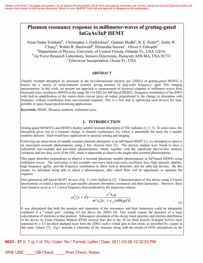
Measured IV curves for PLS022 at T = 295 and 20 K are presented in Fig. 7 (left). The Isd,sat data and fits as a function of gate voltage are plotted in Fig. 7 (right) as symbols for temperatures 20, 80, and 295 K.
Please verify that (1) all pages are present, (2) all figures are acceptable, (3) all fonts and special characters are correct, and (4) all text and figures fit within themargin lines shown on this review document. Return to your MySPIE ToDo list and approve or disapprove this submission.
8023 - 27 V. 1 (p.5 of 10) / Color: No / Format: Letter / Date: 2011-03-28 12:32:53 PM
Fig. 7 (left). Measured IV-Curves for PLS022 with: a = 10 µm and t/a = 0.3 at T = 295 K and T = 20K. (right) Isd-sat vs Vg data
(symbols) and fits (lines).
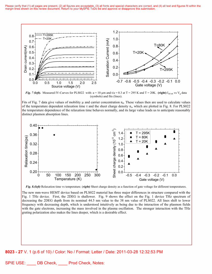
Fits of Fig. 7 data give values of mobility µ and carrier concentration nd. These values then are used to calculate values of the temperature dependent relaxation time τ and the sheet charge density ns, which are plotted in Fig. 8. For PLS022 the temperature dependence of the relaxation time behaves normally, and its large value leads us to anticipate reasonably distinct plasmon absorption lines.
0 50 100 150 200 250 3000.20
0.24
0.28
0.32
0.36
0.40
Rel
axat
ion
time(
ps)
Temperature (K)-0.5 -0.4 -0.3 -0.2 -0.1 0.0
0.00.20.40.60.81.01.21.4
She
et c
harg
e de
nsity
(1012
cm
-2)
Gate voltage (V)
T = 295K T = 80K T = 20K
Fig. 8.(left) Relaxation time vs temperature. (right) Sheet charge density as a function of gate voltage for different temperatures.
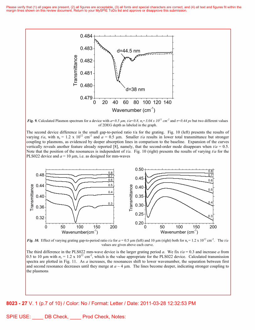
The new mm-wave HEMT device based on PLS022 material has three major differences in structure compared with the Fig. 1 THz device. First, the 2DEG is shallower. Fig. 9 shows the effect on the Fig. 1 device THz spectrum of decreasing the 2DEG depth from its nominal 44.5 nm value to the 38 nm value of PLS022. All lines shift to lower frequency with decreasing depth, which is understood intuitively as being due to the interaction of the plasmon fields with the gate electrons, increasing the mass involved in the plasma oscillation. The stronger interaction with the THz grating polarization also makes the lines deeper, which is a desirable effect.
Please verify that (1) all pages are present, (2) all figures are acceptable, (3) all fonts and special characters are correct, and (4) all text and figures fit within themargin lines shown on this review document. Return to your MySPIE ToDo list and approve or disapprove this submission.
8023 - 27 V. 1 (p.6 of 10) / Color: No / Format: Letter / Date: 2011-03-28 12:32:53 PM
SPIE USE: ____ DB Check, ____ Prod Check, Notes:
0 20 40 60 80 100 120 1400.479
0.480
0.481
0.482
0.483
0.484
Tran
smitt
ance
Wavenumber (cm-1)
d=44.5 nm
d=38 nm
Fig. 9. Calculated Plasmon spectrum for a device with a=0.5 µm, t/a=0.8, ns=3.04 x 1011 cm-2 and τ=0.44 ps but two different values
of 2DEG depth as labeled in the graph.
The second device difference is the small gap-to-period ratio t/a for the grating. Fig. 10 (left) presents the results of varying t/a, with ns = 1.2 x 1012 cm-2 and a = 0.5 µm. Smaller t/a results in lower total transmittance but stronger coupling to plasmons, as evidenced by deeper absorption lines in comparison to the baseline. Expansion of the curves vertically reveals another feature already reported [8], namely, that the second-order mode disappears when t/a = 0.5. Note that the position of the resonances is independent of t/a. Fig. 10 (right) presents the results of varying t/a for the PLS022 device and a = 10 µm, i.e. as designed for mm-waves
0 50 100 150 200
0.32
0.36
0.40
0.44
0.48
Tran
smitt
ance
Wavenumber(cm-1)
0.80.70.6
0.5
0.4
0.3
0 50 100 150 2000.20
0.25
0.30
0.35
0.40
0.45
0.50
Tran
smitt
ance
Wavenumber (cm-1)
0.80.7
0.6
0.5
0.4
0.3
Fig. 10. Effect of varying grating gap-to-period ratio t/a for a = 0.5 µm (left) and 10 µm (right) both for ns = 1.2 x 1012 cm-2. The t/a
values are given above each curve.
The third difference in the PLS022 mm-wave device is the larger grating period a. We fix t/a = 0.3 and increase a from 0.5 to 10 µm with ns = 1.2 x 1012 cm-2, which is the value appropriate for the PLS022 device. Calculated transmission spectra are plotted in Fig. 11. As a increases, the resonances shift to lower wavenumber, the separation between first and second resonance decreases until they merge at a ~ 4 µm. The lines become deeper, indicating stronger coupling to the plasmons
Please verify that (1) all pages are present, (2) all figures are acceptable, (3) all fonts and special characters are correct, and (4) all text and figures fit within themargin lines shown on this review document. Return to your MySPIE ToDo list and approve or disapprove this submission.
8023 - 27 V. 1 (p.7 of 10) / Color: No / Format: Letter / Date: 2011-03-28 12:32:53 PM
SPIE USE: ____ DB Check, ____ Prod Check, Notes:
0 50 100 150 2000.20
0.25
0.30
0.35
0.40
2μm
Tran
smitt
ance
Wavenumber(cm-1)
10μm
0.5μm
Fig. 11. Effect of changing grating period for PLS022 with t/a = 0.3 and ns = 1.2 x 1012 cm-2. Values of a are given below
corresponding peaks.
Gate-bias is the means of tuning the plasmon resonances. We explore the effect of gate bias on the calculated PLS022 mm-wave resonances in Fig. 12 Increasing the negative gate voltage decreases the sheet charge density, which shifts the band to lower wavenumbers while making it shallower.
0 10 20 30 40 500.20
0.25
0.30
0.35
0.40
Vg= -0.5
Tran
smitt
ance
Wavenumber(cm-1)
Vg= 0
Fig. 12. Calculated transmission spectra as a function of gate voltage for PLS022 HEMT device with a = 10 µm, t/a = 0.3. The
extremes of the Vg range are indicated next to their corresponding curve, with each neighboring curve differing by Vg steps of 0.1 V.
The 40-110 GHz (1.3 – 3.7 cm-1) range of our BWO sources is too narrow to sweep over the full width of mm-wave plasmon resonances. The BWO ranges are plotted together with an expanded view of the Fig. 12 curves in Fig. 13. The main feature of these data is that the slope dT/df is decreasing as more negative gate bias is applied.
Please verify that (1) all pages are present, (2) all figures are acceptable, (3) all fonts and special characters are correct, and (4) all text and figures fit within themargin lines shown on this review document. Return to your MySPIE ToDo list and approve or disapprove this submission.
8023 - 27 V. 1 (p.8 of 10) / Color: No / Format: Letter / Date: 2011-03-28 12:32:53 PM
SPIE USE: ____ DB Check, ____ Prod Check, Notes:
0.0 0.5 1.0 1.5 2.0 2.5 3.0 3.5 4.00.24
0.26
0.28
0.30
0.32
0.34
0.36
0.38
Tran
smitt
ance
Wavenumber(cm-1)
Vg= 0
Vg= -0.5
Fig. 13. Calculated Transmittance spectra together with ranges of our three BWOs ( 1.3 – 3.7 cm-1 ) for PLS022 with a = 10µm, t/a = 0.3 The extremes of the Vg range are indicated next to their corresponding curve, which each curve differing from its neighbors by
0.1 V. Horizontal bars indicate the ranges of our three BWO heads.
We have the opportunity to modulate the frequency of the BWO with modulation amplitude Δf. We propose to synchronously lock-in amplify the measured source-drain current ISD. Supposing that there is some effect on channel conductance due to the absorption by plasmons, whose absorptance A = 1-T-R, then the lock-in output will be proportional to |(dT/df)|Δf.
Fig. 14 presents dT/df from the transmittance spectra calculated in Fig. 13. A record of lock-in output for different Vg values should produce a set of points corresponding to a vertical slice through the calculated curves in Fig. 14. By choosing different center frequencies, we should be able to reproduce the complete curves shown in Fig. 14 over the range accessible to our BWOs. Those ranges are indicated in the figure.
0.0 0.5 1.0 1.5 2.0 2.5 3.0 3.5 4.0-0.06
-0.05
-0.04
-0.03
-0.02
-0.01
0.00
dT/d
f
Wavenumber(cm-1)
Vg= 0
Vg= -0.5
Fig. 14. Calculated dT/df spectra in BWO range ( 1.3 – 3.7 cm-1 ) for PLS022 with a = 10 µm, t/a=0.3. The extremes of the Vg range
are indicated next to their corresponding curve, with each curve differing from its neighbors by 0.1 V. Horizontal bars indicate our BWO ranges.
Please verify that (1) all pages are present, (2) all figures are acceptable, (3) all fonts and special characters are correct, and (4) all text and figures fit within themargin lines shown on this review document. Return to your MySPIE ToDo list and approve or disapprove this submission.
8023 - 27 V. 1 (p.9 of 10) / Color: No / Format: Letter / Date: 2011-03-28 12:32:53 PM
SPIE USE: ____ DB Check, ____ Prod Check, Notes:
4. SUMMARY Two different InGaAs/InP HEMT devices each fabricated from wafers with different structures were characterized and studied for the possibility of having resonant plasmon absorption. The first HEMT device based on wafer PLS015A was found unsuitable because small relaxation time and excessive broadening indicated the absence of significant resonant absorption. The device based on wafer PLS022A, with suitable grating gate, was found to have mm-wave absorption peak that responds to gate bias. Expectations for the detection of a corresponding electrical response to mm-wave radiation from frequency modulated BWOs were calculated. .
5. ACKNOWLEDGMENTS This work was supported by AFOSR grant FA95501010030, Program Manager Gernot Pomrenke.
REFERENCES
[1] H. Saxena, R. E. Peale and W. R. Buchwald, “Tunable two-dimentional Plasmon resonances in an InGaAs/InP HEMT”, J. Appli. Phys. 105, 113101 (2009).
[2] S. J. Allen, D. C. Tsui, and R. A. Logan, “Observation of the Two-Dimensional Plasmon in Silicon Inversion Layers.” Phys. Rev. Lett. 38, 980 (1977).
[3] A. V. Muravjov, D. B. Veksler, X. Hu, R. Gaska, N. Pala, H. Saxena, R. E. Peale, M.S. Shur “Resonant terahertz absorption by plasmons in grating-gate GaN HEMT structure” Proc. SPIE 7311-12 (2009).
[4] X. G. Peralta, S. J. Allen, M. C. Wanke, N. E. Harff, J. A. Simmons, M. P. Lilly, J. L. Reno, P. J. Burke, and Eisenstein, “Terahertz photoconductivity and plasmon modes in double-quantum-well field-effect transistors”, Appl. Phys. Lett. 81, 1627 (2002).
[5] R. E. Peale, H. Saxena, W. R. Buchwald, G. C. Dyer, S. J. Allen, Jr. “Tunable THz plasmon resonances in InGaAs/InP HEMT,” Proc. SPIE 7311-17 (2009).
[6] R. E. Peale, H. Saxena, W. R. Buchwald, G. Aizin, A. V. Muravjov, D. B. Veksler, N. Pala, X. Hu, R. Gaska, M. S. Shur, “Grating-gate tunable plasmon absorption in InP and GaN based HEMTs,” Proc. SPIE 7467-25 (2009).
[7] J. W. Cleary, R. E. Peale, H. Saxena, and W. R. Buchwald. “Investigation of plasmonic resonances in the two-dimensional electron gas of an InGaAs/InP high electron mobility transistor.” Proc. SPIE 8023-33 (2011).
[8] W. R. Buchwald, H. Saxena, R. E. Peale, “Tunable Far-IR Detectors/Filters Based on Plasmons in Two Dimensional Electron Gases in InGaAs/InP Heterostructures,” Proc. SPIE 6678-32 (2007).
Please verify that (1) all pages are present, (2) all figures are acceptable, (3) all fonts and special characters are correct, and (4) all text and figures fit within themargin lines shown on this review document. Return to your MySPIE ToDo list and approve or disapprove this submission.
8023 - 27 V. 1 (p.10 of 10) / Color: No / Format: Letter / Date: 2011-03-28 12:32:53 PM