102
PLC Front-end Curtis Mayberry Texas Instruments HPA Linear Applications 8/19/11
| Date post: | 21-Dec-2015 |
| Category: |
Documents |
| Upload: | marylou-grant |
| View: | 221 times |
| Download: | 1 times |

PLC Front-end
Curtis Mayberry
Texas Instruments
HPA Linear Applications
8/19/11

Background
• Student at Iowa State University
• Originally from Ames, IA
• Interest in Analog applications and design
• Graduating December 2011

Coop Term Goals
• Complete PLC Front-end reference design including:– Schematic
– Layout
– Testing
– Documentation
• Continue developing analog circuit analysis skills
• Create a board-level analog circuit design
• Learn about applications engineering and its role in TI’s business
• Learn about TI as an employer

Programmable Logic Controller
• Programmable automation controller
• Used in a variety of industries including the automotive, chemical, and food industries
• Microcontroller offers reprogrammable real-time
control solution
• 4 major Components: – Power supply– Controller– Communications– Input/Output
• Universal voltage Input: 0-5v, ±5v, 0-10v, ±10v• Current loop sensor communication: 0-20mA, 4-20mA• Temperature sensors: thermistor, RTD, thermocouple• Pressure, flow, level, vibration and motion sensors• Digital I/O (GPIO)• Analog Output (DAC8760)

Motivation
• #1 collateral request from FAEs
• Existing ADI reference design
• Customer Requests and New Customer Opportunities
Project Definition
• PLC Analog Front-End
• Focus on analog Inputs:– Universal voltage Input: 0-5v, ±5v, 0-10v, ±10v
– Current loop sensor communication: 0-20mA, 4-20mA
– Temperature sensors: thermistor, RTD, thermocouple
• SM-USB-Dig controller
• Labview Interface to SM-USB-Dig
• Documentation– Create design review and final presentation
– Ensure a smooth transition to next stage of project

Block Diagram
RTDTC
Thermistor+/-10v, +/-5v
4-20mA
Signal Conditioning
MicrocontrollerADC
High-Accuracy
Super-Mini DigLabview
Stage 1 Stage 2
DAC
Stage 1 Only

Implementation

Schematic
• Schematic design review
• Minor schematic design revisions made following review

Layout
• Optimized Analog inputs– Short, symmetric traces
• Recessed power and control circuitry
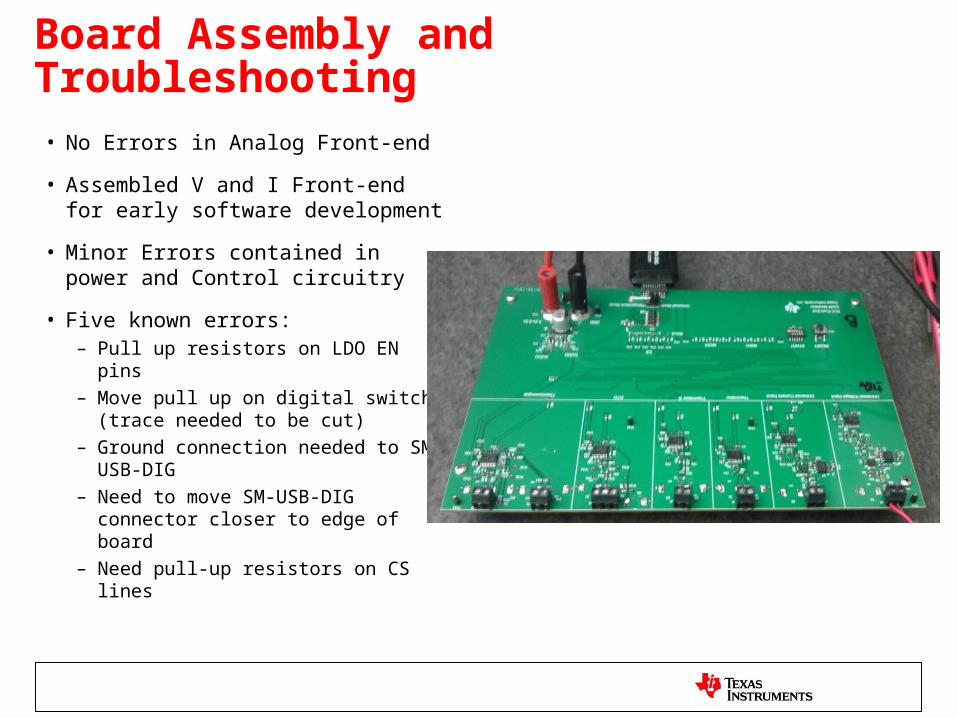
Board Assembly and Troubleshooting
• No Errors in Analog Front-end
• Assembled V and I Front-end for early software development
• Minor Errors contained in power and Control circuitry
• Five known errors:– Pull up resistors on LDO EN pins– Move pull up on digital switch (trace
needed to be cut)– Ground connection needed to SM-
USB-DIG– Need to move SM-USB-DIG
connector closer to edge of board– Need pull-up resistors on CS lines

Software
• Started with SM-Dig shell
• Added CS control to select front-end
• Added DMM Control
• Added Data logging
• Added Data Displays for 6 front-ends
• Added configuration capabilities
for all 6 front-end modules
Labview Interface Front Panel
Labview Interface DMM Control
Testing: Temperature Sensing

Testing: Temperature Sensing
• All Temperature Sensors were submerged and read between 0 oC and 125oC
• Thermal bath wasn’t settling at negative temperatures
• Post-processed 3 point calibration
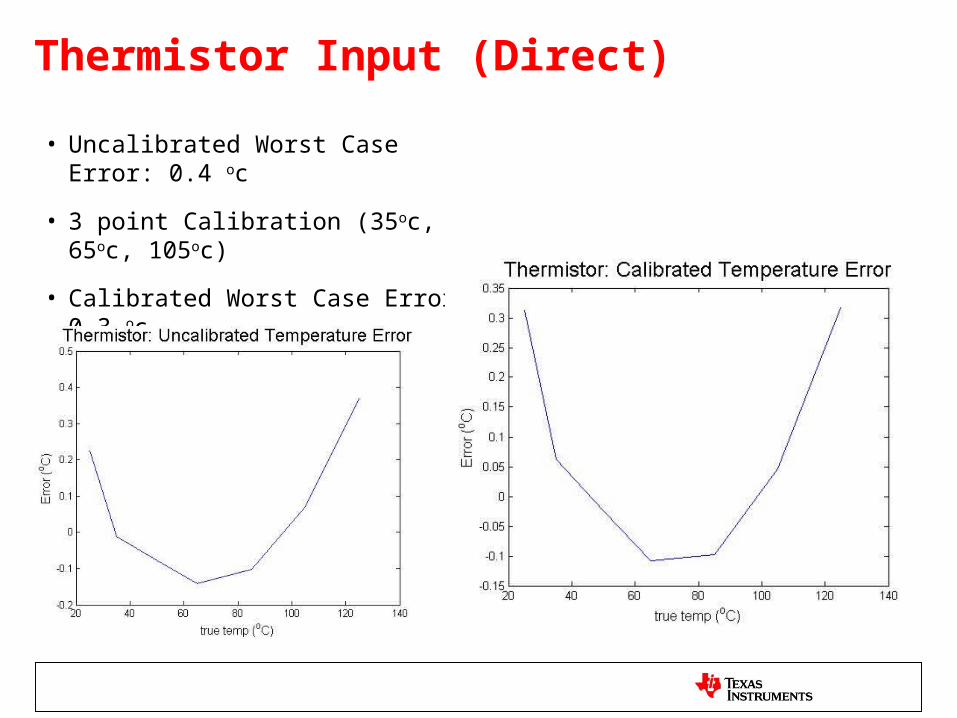
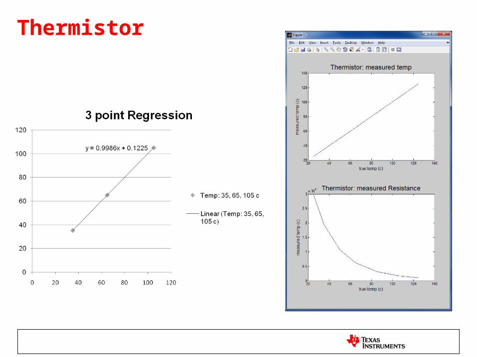
Thermistor Input (Direct)
• Uncalibrated Worst Case Error: 0.4 oc
• 3 point Calibration (35oc, 65oc, 105oc)
• Calibrated Worst Case Error: 0.3 oc– 0.24% accuracy

Thermistor B Input (Bridge)
• Uncalibrated Worst Case Error: 0.9 oc
• 3 point Calibration (35oc, 65oc, 105oc)
• Calibrated Worst Case Error: 0.38 oc– 0.304% Accuracy

RTD Input
• Outlier Removed at 15oC
• Uncalibrated Worst Case Error: 0.9 oc
• 3 point Calibration (35oc, 65oc, 105oc)
• Calibrated Worst Case Error: 0.015 oc– 0.012%

Thermocouple
• Uncalibrated Worst Case Error: 1.2 oc
• 3 point Calibration (35oc, 65oc, 105oc)
• Calibrated Worst Case Error: 0.4 oc– 0.32% error

Results: Temperature Sensing
Maximum calibrated Error 0oC – 125oC
• Thermistor: 0.3oC
• Thermistor B: 0.38oC
• RTD: 0.015 oC
• Thermocouple: 0.4oCError Summary
Calibrated UncalibratedMag (oC) Percent Mag (oC) Percent
Thermistor 0.3 0.24% 0.4 0.32%Thermistor B 0.38 0.30% 0.9 0.72%RTD 0.015 0.01% 0.9 0.72%Thermocouple 0.4 0.32% 1.2 0.96%

Testing: Universal Inputs

Testing: Universal Inputs
• Post-processed 3 point calibration
• Tested using a Fluke precision voltage and current source in 0.5 V or 0.5 mA step size
• Input measured using HP 8.5 digit digital multimeter
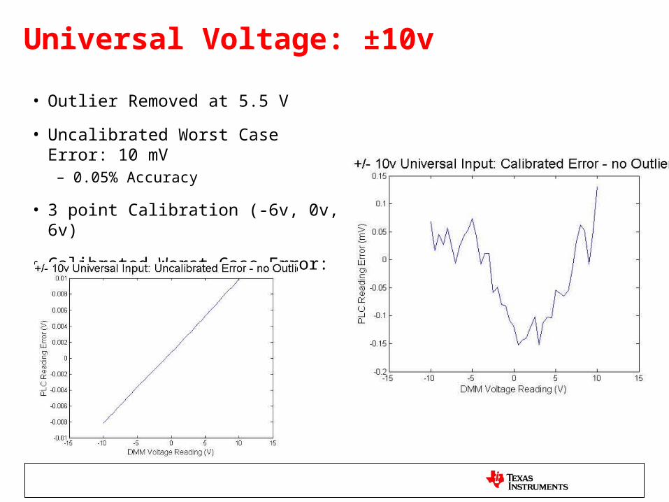
Universal Voltage: ±10v
• Outlier Removed at 5.5 V
• Uncalibrated Worst Case Error: 10 mV– 0.05% Accuracy
• 3 point Calibration (-6v, 0v, 6v)
• Calibrated Worst Case Error: 0.153 mV– 0.000765% Accuracy

Universal Voltage: 0 - 10v
• Outlier Removed at 5.5 V
• Uncalibrated Worst Case Error: 10 mV– 0.1% Accuracy
• 3 point Calibration (2v, 5v, 8v)
• Calibrated Worst Case Error: 0.35 mv– 0.00175% Accuracy
• Worse than +/-10v
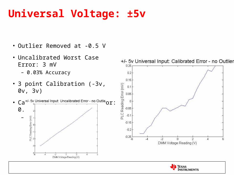
Universal Voltage: ±5v
• Outlier Removed at -0.5 V
• Uncalibrated Worst Case Error: 3 mV– 0.03% Accuracy
• 3 point Calibration (-3v, 0v, 3v)
• Calibrated Worst Case Error: 0.25 mV– 0.0025%

Universal Voltage: 0 - 5v
• Uncalibrated Worst Case Error: 2.5 mV
– 0.05% Accuracy
• 3 point Calibration (0.5v, 2.5v, 4.5v)
• Calibrated Worst Case Error: 0.15 mV– 0.003% Accuracy
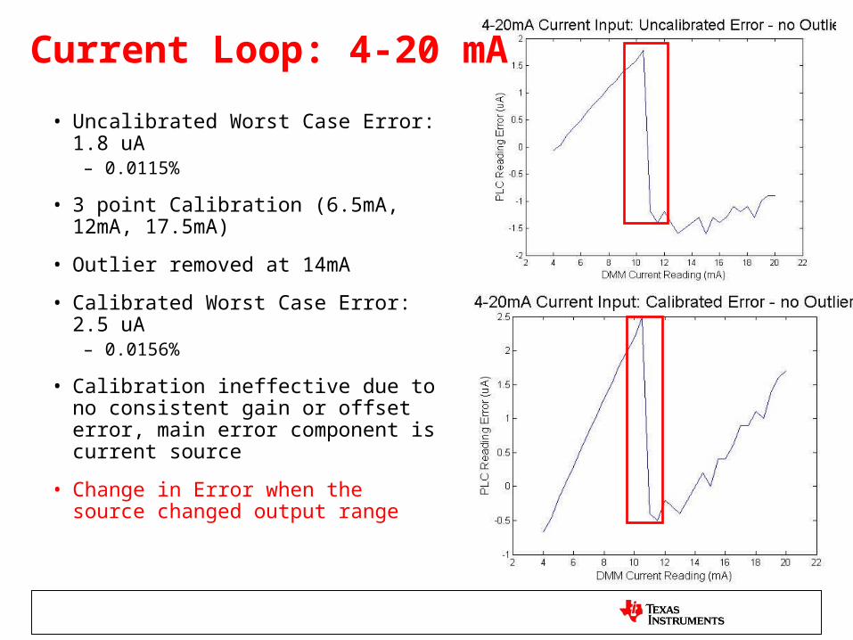
Current Loop: 4-20 mA
• Uncalibrated Worst Case Error: 1.8 uA– 0.0115%
• 3 point Calibration (6.5mA, 12mA, 17.5mA)
• Outlier removed at 14mA
• Calibrated Worst Case Error: 2.5 uA– 0.0156%
• Calibration ineffective due to no consistent gain or offset error, main error component is current source
• Change in Error when the source changed output range

Current Loop: 0-20 mA
• Uncalibrated Worst Case Error: 22uA– 0.11% Accuracy
• 3 point Calibration (3.5mA, 10mA, 16.5mA)
• Calibrated Worst Case Error: 21 uA– 0.105% Accuracy

Results: Universal Front-Ends
Calibrated maximum error:
• Universal V– ±10 v: 0.153 mV
– 0-10 v: 0.35 mV
– ±5 v: 0.25 mV
– 0-5 v: 0.15 mV
• Current Loop– 4-20 mA: 2.5 uA
– 0-20 mA: 21 uA
Error SummaryCalibrated Uncalibrated
Mag Percent Mag Percent±10v 0.153mV 765u% 10mV 0.05%
0-10v 0.35mV 1.75m% 10mV 0.10%±5v 0.25mV 2.5m% 3mV 0.03%
0-5v 0.15mV 3m% 2.5mV 0.05%

Accomplishments
• Completed PLC Front-End Design– PLC Research– Sensor Research– Component Selection– Schematic Design and Review– Layout Design and Review– Fabrication– Software– Debugging– Testing
• Completed Forum Post
• Learned a lot about board-level development, Op-amps, and about TI’s business

Other Accomplishments
• Volunteered:– Day of Hope
– Disability Connection Carnival
• Networked with teammates and other coops
• Learned about analog applications
• Learned about the relationship between field and factory applications engineering
• Developed a better understanding of all the engineering roles

Project Continuation and Career Plans
Final Goal: Complete PLC Reference Design utilizing TI parts
• Progress will continue during second stage
• Potential Microcontroller TI 32-bit Stellaris LM3S1Z16
• Potential output DAC: DAC8760
Career Plans:
• Attend graduate school for analog design
• Return to TI for another Coop Experience as a graduate student

Feedback
• Great Project– Interesting and rewarding
– Well-defined and complete
• Excellent Mentoring by Pete and Collin– Given Freedom to work independently while still having support available
– Great job with on-boarding and providing the resources I needed
– Great teachers for both Technical and non-technical material
• AFA conference and Tucson Testing Trip were Great Opportunities
• CORT relocation service hard to work with before coming to TI

Thank You
• Special Thank You to my mentors:
Collin Wells
Pete Semig
• Also to my managers:
Art Kay
Matt Hann
• Data Converter Applications TeamTom Hendrick, Greg Hupp, Kevin Duke, Tony Calabria

Appendices
• Appendix A: Elaborated Testing Results
• Appendix B: Design review

Appendix A: Elaborated Testing Results
Calibration Curves, raw data plots, resistance plots
Thermistor

Thermistor B
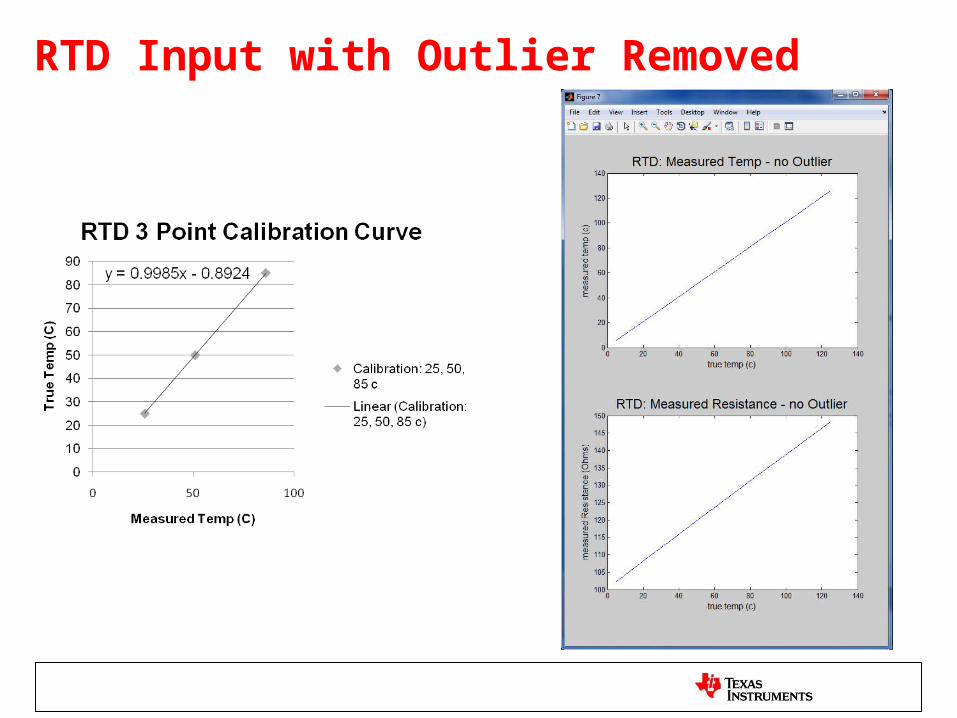
RTD Input with Outlier Removed

RTD Input with Outlier at 15oc

Thermocouple

Universal Voltage: ±10v – no outlier

Universal Voltage: ±10v – with Outlier

Universal Voltage: 0 - 10v – no Outlier

Universal Voltage: 0 - 10v –with Outlier

Universal Voltage: ±5v – no Outlier

Universal Voltage: ±5v - with Outlier

Universal Voltage: 0 - 5v

Current Loop: 4-20 mA - no Outlier

Current Loop: 4-20 mA with Outlier

Current Loop: 0-20 mA - no Outlier
Appendix B: Design Review
Original Design Review
7-5-11

Revised Project Description

Block Diagram
RTDTC
Thermistor+/-10v, +/-5v
4-20mA
Signal Conditioning MicrocontrollerADC
Cost-Effective
High-Accuracy
Super-Mini DigLabview
Stage 1 Stage 2
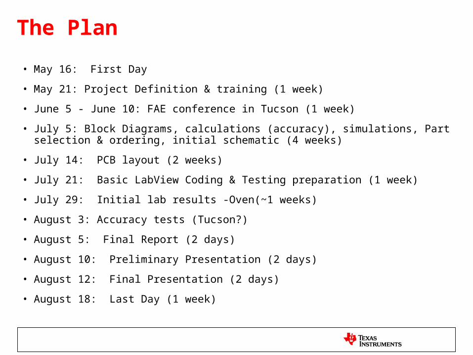
The Plan
• May 16: First Day
• May 21: Project Definition & training (1 week)
• June 5 - June 10: FAE conference in Tucson (1 week)
• July 5: Block Diagrams, calculations (accuracy), simulations, Part selection & ordering, initial schematic (4 weeks)
• July 14: PCB layout (2 weeks)
• July 21: Basic LabView Coding & Testing preparation (1 week)
• July 29: Initial lab results -Oven(~1 weeks)
• August 3: Accuracy tests (Tucson?)
• August 5: Final Report (2 days)
• August 10: Preliminary Presentation (2 days)
• August 12: Final Presentation (2 days)
• August 18: Last Day (1 week)

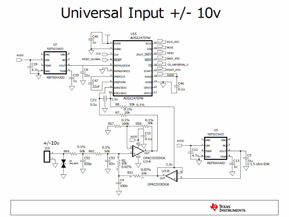
Universal Inputs
0-10v and +/- 10v, 0-5v and +/- 5v, 4-20mA

Universal Voltage Input
• 0-5v, 0-10v, +/- 5v and +/- 10v universal voltage input
• Change resistance values to change input voltage levels
• Second order RC filter with poles at 39 Hz and 3900Hz
• Opamp to scale down input
• 2.5v reference generated to scale input
• Opa2333: Low offset voltage and drift, rail-to-rail input, dual opamp part


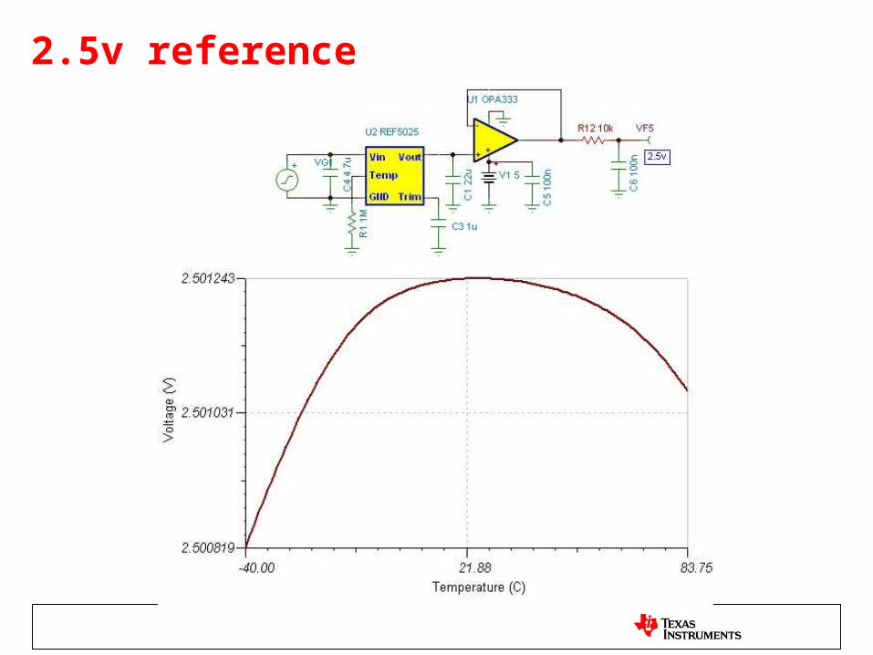
Noise Calculations: Voltage Reference
• 2.5v Reference– REF5025: 625nVRMS
– OPA333: 869 nVRMS
– Filter KTC noise: 202.8nVRMS
– Reference Output 10kΩ: 202.8 nVRMS
– Total Noise: 1.108µVRMS
RMSHznV
BB
n
HznV
nVHzen
HzHzBW
86963.249)55(
63.249)57.1)(159(
noise) 1/f (no 55 :noise BB
RMS
KJ
R
n
nV
Hzkken
HzHzBW
8.202
)9.249)(10)(15.298)(1038.1(4
9.249)57.1)(15.159(
23
RMSKJ
filter nVnF
ken 84.202
100
)15.298)(1038.1( 23
RMSREF VnVnVnVen 108.1)625()8.202(2)869( 222
– Current Noise: 26.34nVRMS (negligible)
RMS
HznV
BB
nV
kHzen
34.26
)67.16(63.249)100(
RMSppREF nVVen 625)5.7(21
5025
Noise Calculations
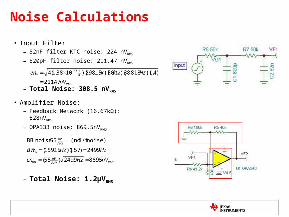
• Input Filter – 82nF filter KTC noise: 224 nVRMS
– 820pF filter noise: 211.47 nVRMS
– Total Noise: 308.5 nVRMS
• Amplifier Noise:– Feedback Network (16.67kΩ):
828nVRMS
– OPA333 noise: 869.5nVRMS
– Total Noise: 1.2µVRMS
RMSHznV
BB
n
HznV
nVHzen
HzHzBW
5.8699.249)55(
9.249)57.1)(15.159(
noise) 1/f (no 55 :noise BB
RMS
KJ
R
nV
Hzkken
47.211
)4.1)(818.38)(50)(15.298)(1038.1(4 23

Noise Calculations: Total
• ADC V+ input noise total: 1.503µVRMS
• ADC V- input noise total:1.089uVRMS
RMS
kk
kk
V
V
nVVnVVen
503.1
)8.202()2.1)2.1(()5.308))(2.1(()108.1))(2.1(( 2
filteroutput
2
amplifier
2
filterinput
1201002
Ref
12020
RMSV VnVnVnVen 089.1)625()8.202()869( 222

Noise Calculations: Bringing it all together
• ADC noise: 1.35 µVRMS
– Noise at Apga =1 and 5 SPS
FS of %000358.060
771.13295.2
)089.1()503.1()35.1(noiseOuput 2
-V
2
V
2
ADC
bits
VV
VVV
PPRMS
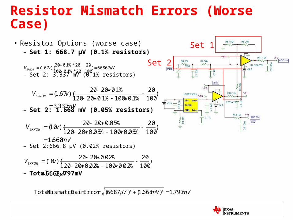
Resistor Mismatch Errors (Worse Case)
• Resistor Options (worse case)– Set 1: 668.7 µV (0.1% resistors)
– Set 2: 3.337 mV (0.1% resistors)
– Set 2: 1.668 mV (0.05% resistors)
– Set 2:666.8 µV (0.02% resistors)
– Total: 1.797mV
mV
vVERROR
337.3
)100
20
%1.0100%1.020120
%1.02020)(67.1(
VvVERROR 67.668)100
20
20*%1.0100
20*%1.020)(67.1(
mV
vVERROR
668.1
)100
20
%05.0100%05.020120
%05.02020)(10(
V
vVERROR
8.666
)100
20
%02.0100%02.020120
%02.02020)(10(
mVmVV 797.1)668.1()7.668(ErrorGain Mismatch Total 22
Set 1
Set 2

Resistor Tolerance Monte Carlo Simulation
• Ran Monte Carlo Simulation using 0.1% resistors
• 2.5 mV max error on output
• Used an ideal op-amp to isolate the error source
• Small variation between resistor tolerances

Error Estimation
• ADC– 15µV offset– INL: 6 ppm– Gain Error: 0.02%– External Reference: 0.05%*2.024V = 1.024 mV– Total: 1.230 mV
• Level shifting OPA2333– Offset: 10 µV– Offset drift: 0.05 µV/oc– CMRR >106 dB– PSRR: 5 µV/V (max)
• 2.5v Reference OPA2333– Offset: 10 µV– Offset drift: 0.05 µV/oc (3µV over 25oC ± 60oC temperature range)– CMRR >106 dB– PSRR: 5 µV/V (max)
Vv 244*10
66
Vv 8004*0002.0
20,,, 10
CMRR
dcmincmincmcmo AVVAV
PSRRAVV dPSnoiseoffset PS o,

Error Estimation
• Resistor Mismatch: 1.797 mV
• REF5025 2.5v reference: 1.25 mV offset is cancelled out
• Total:
with no “interference”: 2.178 mV
2PSnoise
220,
2222 )(2)10(2))25)(05.0((2)797.1()10(2)230.1( PSRRAVAVCTmVVmV d
CMRR
dcmino
C
Vo
mVmVmV 178.2)797.1()23.1( 22

Simulation: +/- 10v

Simulation: +/- 5v


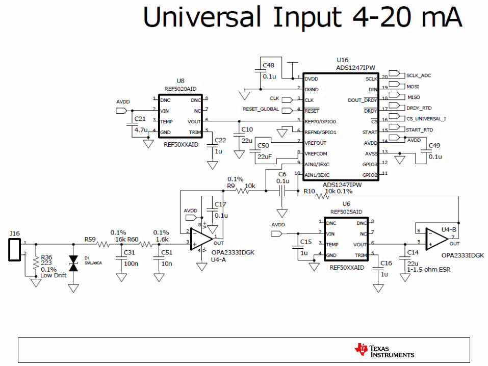
Universal Current input
• 4-20mA
• Second order RC filter
• Internal 2.048v reference
• 221Ω shunt converts 4-20mA to 884mV-4.420V
• OPA2333: Rail-to-Rail common mode input, low offset voltage and drift

Simulation
2.5v reference
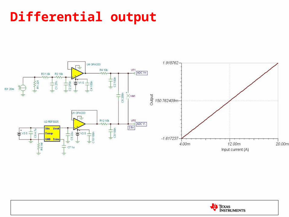
Differential output

Noise Analysis
• OPA333 buffer noise: 869.5 nVRMS
• Resistor Noise– 10kΩ: 202.8 nV– 16kΩ: 123 nV– 1.6kΩ: 31.1 nV
• V+ Total Noise: 901.8 nVRMS
• V- Total Noise: 1.089 µVRMS (Same as Vinput V-)
• ADC noise: 1.35 µVRMS – Noise at Apga =1 and 5 SPS
• Total noise: 11.729 µVPP
RMSHznV
BB
n
HznV
nVHzen
HzHzBW
5.8699.249)55(
9.249)57.1)(15.159(
noise) 1/f (no 55 :noise BB
RMSV VnVnVnVen 089.1)625()8.202()869( 222
FS of %1029249
729.11954.1
)089.1()8.901()35.1(noiseOuput
6
2
-V
2
V
2
ADC
bits
VV
VnVV
PPRMS

Error Estimation
• ADC– 15µV offset– INL: 6 ppm– gain error: 0.02%– Noise error: 7.78 µVpp– External Reference: 1.024 mV
• Shunt resistor tolerance: 20mA*221*.1% =4.42 mV
• Level shifting OPA333– Offset: 10 µV– Offset drift: 0.05 µV/oc– CMRR >106 dB– PSRR: 5 µV/V (min)
• 2.5v Reference OPA333– Offset: 10 µV– Offset drift: 0.05 µV/oc (3µV over 25oC ± 60oC temperature range)– CMRR >130 dB– PSRR: 2 µV/V
• REF5025: 1.25mV
• Total
Vv 244*10
66
Vv 8004*0002.0
20,,, 10
CMRR
dcmincmincmcmo AVVAV
PSRRAVV dPSnoiseoffset PS o,
mVmVmVVV 669.4)2.4()25.1()10(2)839( 2222
2PSnoise
220,
22222 )(2)10(2))25)(05.0((2)2.4()25.1()10(2)839( PSRRAVAVCTmVmVVV d
CMRR
dcmino
C
Vo


Temperature Sensors
Thermistor
RTD
Thermocouple
Targeted industrial temperature range: -40oc to 85oc

Thermistor
• Temperature proportional to resistance
• Calibrated: 25oC and 85oC
• NTC thermistor– 30kΩ ±1% @ 25oC
• 2 Designs: – Single-ended – Bridged
)1
15.3981
(3992exp(
30
%1399285/25
Tk
kR


Simulation

Error Estimation
• Resistor Mismatch: 374.81µV
• Current Accuracy:0v– Ratio metric measurement
• Thermistor Errors: 5.027 mV– Thermistor 25oC R-tolerance: 3.731mV (R±1%)
– Beta Error: 3.37 mV (Beta±1%)
• ADC Errors: – 15µV offset
– INL: 6 ppm
– gain error: 0.02%
– External reference R: 2mV
• Minimum 4.4 mV/oC
• Total Error: 5.425mV (~1.23oC)
V
kkk
kkkA
81.374
)15001.*3060
)001.*3030)(30()(50(Error mismatch R
Vv 122*10
66
Vv 4002*0002.0
mV
kkk
kkkA
731.3
)20001.*4080
)001.*4040)(40()(50(Error -R thermistor
Output Voltage Temperature Dependence
0
100
200
300
400
500
600
700
800
0 20 40 60 80 100
temp (degrees C)
Ou
tpu
t V
olt
age
(mV
)
B nominal
B + 1%
B - 1%


Simulation

Error Estimation
• Resistor Mismatch: 1.677mV (0.1% resistors)
• Current Accuracy: 0v– Ratio metric reading (external ref)– Mismatch between current sources:
• ±0.15% of FS (50 µV) = 75nV (negligible)
• Thermistor Errors: 5.027 mV– Thermistor 25oC R-tolerance: 3.731mV (R±1%)– Beta Error: 3.37 mV (Beta±1%)
• ADC Errors: 400.5µV– 15µV offset– INL: 6 ppm– gain error: 0.02%
• Minimum 4.4 mV/oC
• Total Error: 5.311mV
mVVmV
VkAmVkA
677.1)750()5.1(Error
750)001.*15)(50(:Right 5.1)001.*30)(50(
22mismatch R
Vv 122*10
66
Vv 4002*0002.0


RTD
• PT100, PT 1000
• Resistance proportional to temperature
• Callendar-Van Dusen equation


Simulation
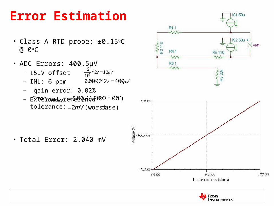
Error Estimation
• Class A RTD probe: ±0.15oC @ 0oC
• ADC Errors: 400.5µV– 15µV offset– INL: 6 ppm– gain error: 0.02%– External reference tolerance:
• Total Error: 2.040 mV
Vv 122*10
66
Vv 4002*0002.0
case)(worst 2
)001.*20)(100(
mV
kAErrorREFERENCE


Thermocouple
• Seebeck effect
• Need to measure voltage across the element
• Cold junction compensation: RTD close to the cold junction
• PCB layout designed to keep the cold junction isothermal with the RTD
• Types: K, J, T, E, N, R, S, B
• Different materials, temperature ranges, TC
• Example: K type: ~55µV/oC


Error Estimation
• RTD Error: 2.040 mV
• Thermocouple element error: Varies by type
• Max element error (using K type): 1.1oC or 0.4%

Digital Interface
SM-USB-DIG

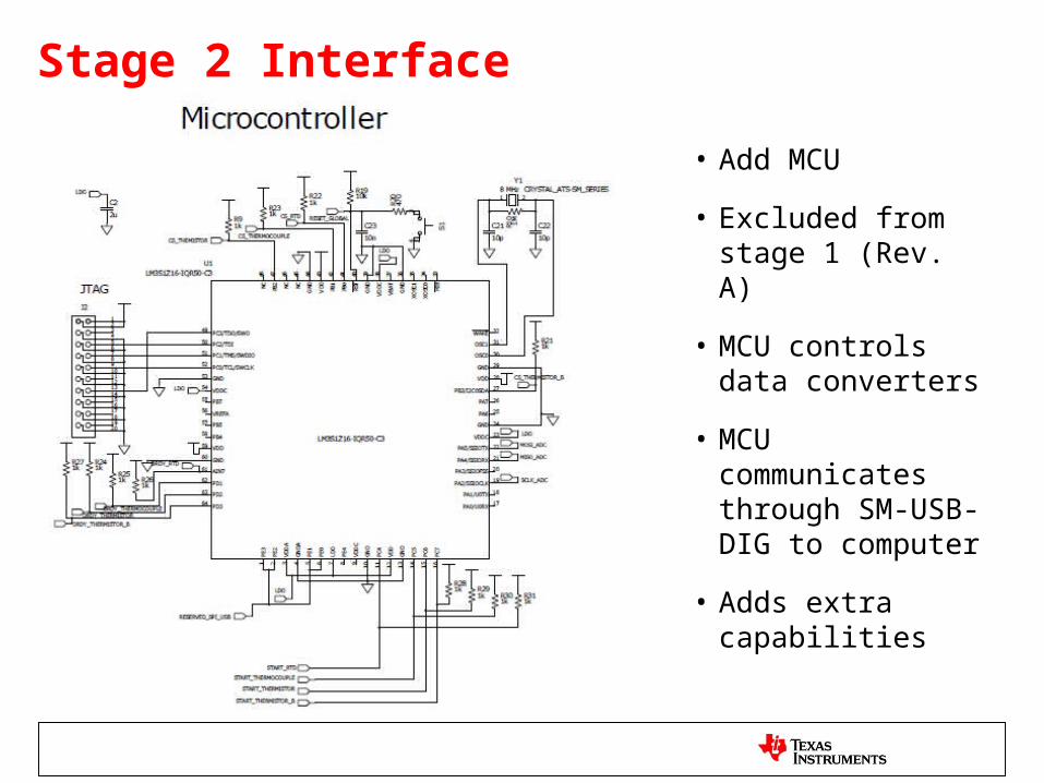
Stage 2 Interface
• Add MCU
• Excluded from stage 1 (Rev. A)
• MCU controls data converters
• MCU communicates through SM-USB-DIG to computer
• Adds extra capabilities

Power
• Powered by a lab supply for prototyping
• Banana plug input jack
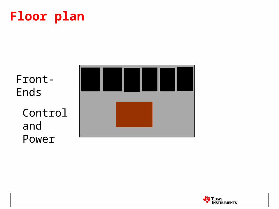
Floor plan
Front-Ends
Control and Power

The Plan
• May 16: First Day
• May 21: Project Definition & training (1 week)
• June 5 - June 10: FAE conference in Tucson (1 week)
• July 5: Block Diagrams, calculations (accuracy), simulations, Part selection & ordering, initial schematic (4 weeks)
• July 14: PCB layout (2 weeks)
• July 21: Basic LabView Coding & Testing preparation (1 week)
• July 29: Initial lab results -Oven(~1 weeks)
• August 3: Accuracy tests (Tucson?)
• August 5: Final Report (2 days)
• August 10: Preliminary Presentation (2 days)
• August 12: Final Presentation (2 days)
• August 18: Last Day (1 week)


