55
PLD (Programmable Logic Device) Saturday, March 12, 2 022 1 ARINDAM CHAKRABORTY LECTURER,DEPT. OF ECE INSTITUTE OF ENGINEERING & MANAGEMENT

PLD(Programmable Logic Device)
Friday, April 21, 2023 1
ARINDAM CHAKRABORTYLECTURER,DEPT. OF ECEINSTITUTE OF ENGINEERING & MANAGEMENT


COMPLEXITYCOMPLEXITY
1905 : Mount Road -Madras 2005: Mount Road -Madras

Integrated Circuit RevolutionIntegrated Circuit Revolution
1958:First integrated circuit (germanium) Built by Jack Kilbyat Texas Instrumentscomponents :Transistors, Resistors and Capacitors
2000: Intel Pentium 4 ProcessorClock speed: 1.5 GHz Transistors: 42 millionTechnology: 0.18μm CMOS

If Transistors are Counted as Seconds If Transistors are Counted as Seconds

Evolution of VLSI
•SSI–Small Scale Integration (GATE < 10 )
•MSI–Medium Scale Integration (10 < GATE < 1000)
Demanded automation of design process Demanded automation of design process CComputer omputer AAid id DDesign started evolving esign started evolving
•LSI–Large Scale Integration (GATE > 1000)
•VLSI–Very Large Scale Integration ( GATE > 100000)

Before ToolsBefore Tools
•Laid out 4004 by hand
–Drawn on paper and photographed
–Demagnified 500 times smaller
•Almost no verification or validation
–Chips may not function properly
–Market may return products
SOLUTION !SOLUTION !

VLSI chip design forced
•Automation of process
•Automation of Simulation based verification
REPLACING REPLACING
Breadboard Techniques HDL Development
Evolution of CAD Tools

Comparison of SizesComparison of Sizes

How Small Are The Transistors?How Small Are The Transistors?

Processor Power TrendsProcessor Power Trends

Evolution in IC ComplexityEvolution in IC Complexity

Design Goals Over TimeDesign Goals Over Time

COMPLEXITYCOMPLEXITY
1905 : Mount Road -Madras 2005: Mount Road -Madras

ROM
F1
F2
A
B
Ci
SIZE OF ROM:-
FOR, ‘n’ No. OF INPUT AND ‘m’ No. OF
OUTPUT
SIZE =2 n x m BITS
SIZE OF ROM:-
FOR, ‘n’ No. OF INPUT AND ‘m’ No. OF
OUTPUT
SIZE =2 n x m BITS
IT IS TRUTH TABLE IN A HARDWARE FORM
OR
WE CAN SAY HARDWARE FOR TRUTH TABLE
IT IS TRUTH TABLE IN A HARDWARE FORM
OR
WE CAN SAY HARDWARE FOR TRUTH TABLE
‘n’ ‘m’
ROM
Read Only Memory (ROM)Read Only Memory (ROM)
Friday, April 21, 2023 15

DECODER(AND ARRAY)
m0m1
m2
m3
m4
m5
m6m7
ai
bi
Ci-1
Si
Ci
DECODER DESIGN
APPLYING 1-BIT FULL ADDERSi = F (1,2,4,7)Ci = F (3,5,6,7)
Friday, April 21, 2023 16
Read Only Memory (ROM)Read Only Memory (ROM)

Read only memory (ROM)
ROM holds programs and data permanently even when computer is switched off
Data can be read by the CPU in any order so ROM is also direct access
The contents of ROM are fixed at the time of manufacture
Access time of between 10 and 50 nanoseconds

Friday, April 21, 2023 19
•PROGRAMMABLE ::
I CAN CHANGE THE APPLICATION
•LOGIC ::
THE VALIDITY OF AN ARGUMENT IS DETERMINED
BY ITS LOGICAL FORM
•DEVICE ::
MACHINE
PLDPLD

Friday, April 21, 2023 20
• Programmable Logic Device(PLD):
A programmable logic devices is an IC’s that user configurableuser configurable
and is capable of implementing implementing logic function
• PLDs ARE :-
I . COMBINATIONAL PLDs
II . SEQUENTIAL PLDs

Friday, April 21, 2023 21
I. COMBINATIONAL
PROGRAMMABLE LOGIC DEVICE (PLD):

DIFFERENT TYPES OF COMBINATIONAL PLDs :-
Fixed AND Array(Decoder)
Programmable OR Array
Input Output
A. Programmable Read Only Memory (PROM) :A. Programmable Read Only Memory (PROM) :
Programmable AND Array
Fixed OR Array
Input Output
B. Programmable Array Logic (PAL) :B. Programmable Array Logic (PAL) :
Programmable AND
Array
Programmable OR Array
Input Output
C. Programmable Logic Array (PLA) :C. Programmable Logic Array (PLA) :
Friday, April 21, 2023 22

DIFFERENT TYPEs OF ROM:-DIFFERENT TYPEs OF ROM:-
ROM (AND & OR ARRAY BOTH ARE FIXED)
PROM (FIXED AND ARRAY & PROGRAMMABLE OR ARRAY)
EPROM (ERASABLE PROM> TO CHANGE MORE TIME)
UVEPROM (OLD TECH.> TO CHANGE THE LOGIC USING UV RAY)
EEPROM(ELECTRICALLY ERASABLE PROM> APPLYING ELEC. PULSES)
EAPROM(ELECTRICALLY ALTERABLE PROM> NEW TECH) OR FLASH MEMORY
Friday, April 21, 2023 23

Types of ROM1. Programmable Read Only Memory (PROM)
• Empty of data when manufactured
• May be permanently programmed by the user
2. Erasable Programmable Read Only Memory (EPROM)
• Can be programmed, erased and reprogrammed
• The EPROM chip has a small window on top allowing it to be erased by shining ultra-violet light on it
• After reprogramming the window is covered to prevent new contents being erased
• Access time is around 45 – 90 nanoseconds
Note: a nanosecond is one billionth of a second!

Types of ROM3. Electrically Erasable Programmable Read Only Memory
(EEPROM)
• Reprogrammed electrically without using ultraviolet light
• Must be removed from the computer and placed in a special machine to do this
• Access times between 45 and 200 nanoseconds4. Flash ROM
• Similar to EEPROM
• However, can be reprogrammed while still in the computer
• Easier to upgrade programs stored in Flash ROM
• Used to store programs in devices
• Access time is around 45 – 90 nanoseconds
Note: a nanosecond is one billionth of a second!

DIFFERENT TYPEs OF ROM:-DIFFERENT TYPEs OF ROM:-
Friday, April 21, 2023 26

DIFFERENT TYPES OF COMBINATIONAL PLDs :-
Fixed AND ArrayFixed AND Array(Decoder)(Decoder)
Programmable OR Programmable OR ArrayArray
InputInput OutputOutput
A. Programmable Read Only Memory (PROM) :A. Programmable Read Only Memory (PROM) :

AND ARRAY
m0m1
m2
m3
m4
m5
m6m7
ai
bi
Ci-1
Si Ci
OR ARRAY
FIXED AND ARRAY & PROGRAMMABLE OR ARRAY
APPLYING 1-BIT FULL ADDERSi = F (1,2,4,7)Ci = F (3,5,6,7)
(A) Programmable Read Only Memory (PROM)
Friday, April 21, 2023 28

Programmable ANDProgrammable AND ArrayArray
Fixed OR Fixed OR ArrayArray
InputInput OutputOutput
B. Programmable Array Logic (PAL) :B. Programmable Array Logic (PAL) :
DIFFERENT TYPES OF COMBINATIONAL PLDs :-
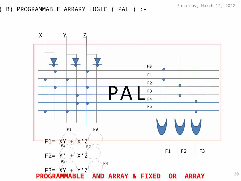
( B) PROGRAMMABLE ARRARY LOGIC ( PAL ) :-
X Y Z
F1 F3
P0
F1= XY + X’Z
F2= Y’ + X’Z
F3= XY + Y’Z
Friday, April 21, 2023
30
P1
P2
P3
P4
P5
P0P1
P2P3
P4P5
F2
PROGRAMMABLE AND ARRAY & FIXED OR ARRAY

PAL Table (Specifications):PAL Table (Specifications):
SIZE OF PAL :SIZE OF PAL :
3 INPUTs3 INPUTs 3 OUTPUT3 OUTPUT 6 PRODUCT TERM6 PRODUCT TERM 2 FOR EACH OUTPUT2 FOR EACH OUTPUT
P0P0 P1P1 P2P2 P3P3 P4P4 P5P5
F1F1 YESYES YESYES NILNIL NILNIL NILNIL NILNIL
F2F2 NILNIL NILNIL YESYES YESYES NILNIL NILNIL
F3F3 NILNIL NILNIL NILNIL NILNIL YESYES YESYES

Programmable ANDProgrammable AND ArrayArray
Programmable OR Programmable OR ArrayArray
InputInput OutputOutput
C. Programmable Logic Array (PLA) :C. Programmable Logic Array (PLA) :
DIFFERENT TYPES OF COMBINATIONAL PLDs :-
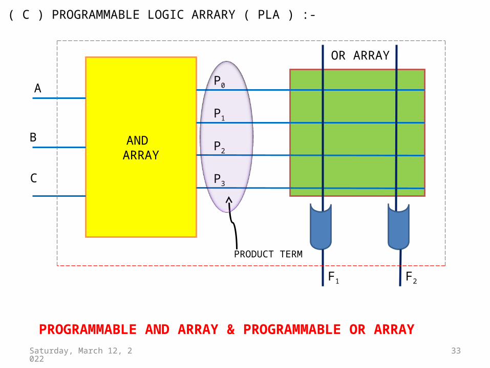
AND ARRAY
P0
P1
P2
P3
A
B
C
F1 F2
OR ARRAY
PROGRAMMABLE AND ARRAY & PROGRAMMABLE OR ARRAY
( C ) PROGRAMMABLE LOGIC ARRARY ( PLA ) :-
PRODUCT TERM
Friday, April 21, 2023 33

( C) PROGRAMMABLE LOGIC ARRARY ( PLA ) :-
X Y Z
F1F2 F3
P0
P1
P2
P3
F1= XY + X’Z
F2= Y’ + X’Z
F3= XY + Y’Z
P0
P1
P3
P2
Friday, April 21, 2023
34
P0
P1
PROGRAMMABLE AND ARRAY & PROGRAMMABLE OR ARRAY

PLA Table (Specifications):PLA Table (Specifications):
SIZE OF PLA :SIZE OF PLA :
3 INPUTs3 INPUTs
4 PRODUCT TERM4 PRODUCT TERM
3 OUTPUT3 OUTPUT

Design PAL :Design PAL :
PAL Table (Specifications):PAL Table (Specifications):
SIZE OF PAL :SIZE OF PAL :
3 INPUTs 6 PRODUCT TERM 3 OUTPUT 2 FOR EACH OUTPUT
P0P0 P1P1 P2P2 P3P3 P4P4 P5P5
F1F1 YESYES YESYES NILNIL NILNIL NILNIL NILNIL
F2F2 NILNIL NILNIL YESYES YESYES NILNIL NILNIL
F3F3 NILNIL NILNIL NILNIL NILNIL YESYES YESYES
F1(a,b,c) = ∑m (0,2)F1(a,b,c) = ∑m (0,2)F2(a,b,c) = ∑m (0,3,4)F2(a,b,c) = ∑m (0,3,4)F3(a,b,c) = ∑m (0,3,4,7)F3(a,b,c) = ∑m (0,3,4,7)

Design PLA :Design PLA :
PLA Table (Specifications):PLA Table (Specifications):
SIZE OF PLA :SIZE OF PLA :
3 INPUTs 6 PRODUCT TERM 3 OUTPUT
P0P0 P1P1 P2P2 P3P3 P4P4 P5P5
F1F1 YESYES NILNIL NILNIL NILNIL NILNIL NILNIL
F2F2 NILNIL YESYES YESYES NILNIL NILNIL NILNIL
F3F3 NILNIL NILNIL NILNIL YESYES YESYES NILNIL
F1(a,b,c) = ∑m (0,2)F1(a,b,c) = ∑m (0,2)F2(a,b,c) = ∑m (0,3,4)F2(a,b,c) = ∑m (0,3,4)F3(a,b,c) = ∑m (0,3,4,7)F3(a,b,c) = ∑m (0,3,4,7)

Programmable Array Logic (PAL) & Programmable Logic Array (PLA) :Programmable Array Logic (PAL) & Programmable Logic Array (PLA) :
Friday, April 21, 2023 38

Friday, April 21, 2023 39
II . SEQUENTIAL II . SEQUENTIAL
PROGRAMMABLE LOGIC DEVICE PROGRAMMABLE LOGIC DEVICE (PLD):(PLD):

DIFFERENT TYPES OF SEQUENTIAL PLDs :-
A. SIMPLE PROGRAMMABLE LOGIC DEVICE (SPLD) :A. SIMPLE PROGRAMMABLE LOGIC DEVICE (SPLD) :
B. COMPLEX PROGRAMMABLE LOGIC DEVICE (CPLD):B. COMPLEX PROGRAMMABLE LOGIC DEVICE (CPLD):
C. FIELD PROGRAMMABLE GATE ARRAY (FPGA) :C. FIELD PROGRAMMABLE GATE ARRAY (FPGA) :
Friday, April 21, 2023 40

Friday, April 21, 2023 41
(I) SIMPLE PROGRAMMABLE LOGIC DEVICE (SPLD) ::(I) SIMPLE PROGRAMMABLE LOGIC DEVICE (SPLD) ::
INPUTINPUTOUTPUTOUTPUT
•An SPLD can implement hundreds of gatesAn SPLD can implement hundreds of gates
Friday, April 21, 2023 42
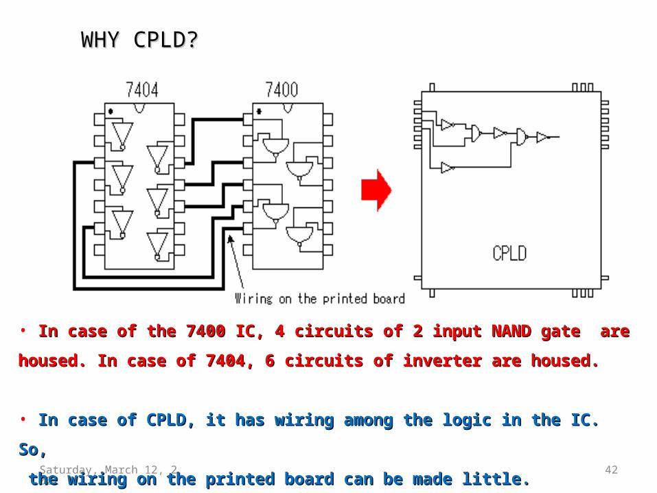
WHY CPLD?WHY CPLD?
• In case of the 7400 IC, 4 circuits of 2 input NAND gate are housed. In case of 7404, 6 In case of the 7400 IC, 4 circuits of 2 input NAND gate are housed. In case of 7404, 6
circuits of inverter are housed.circuits of inverter are housed.
• In case of CPLD, it has wiring among the logic in the IC. So,In case of CPLD, it has wiring among the logic in the IC. So,
the wiring on the printed board can be made little. the wiring on the printed board can be made little.

Friday, April 21, 2023 43
(II) COMPLEX PROGRAMMABLE LOGIC DEVICE (CPLD)::(II) COMPLEX PROGRAMMABLE LOGIC DEVICE (CPLD)::
PROGRAMMABLE SWITCH MATRIXPROGRAMMABLE SWITCH MATRIX

Friday, April 21, 2023 44
• Example CPLD Families ::
Altera MAX 7000 and MAX 9000 families
Atmel ATF and ATV families
Lattice ispLSI family
Lattice (Vantis) MACH family
Xilinx XC9500 family

Friday, April 21, 2023 45
CPLD EXAMPLE ::CPLD EXAMPLE ::

Friday, April 21, 2023 46
(III) FIELD PROGRAMMABLE GATE ARRAY ::(III) FIELD PROGRAMMABLE GATE ARRAY ::
• FPGA, first introduced first introduced by Xilinx in 1984.Xilinx in 1984.
• ItIt is a reprogrammable logic device reprogrammable logic device that
implements multilevel logic.

Friday, April 21, 2023
47
CLB
CLB
CLB
CLB
CLB
CLB
CLB
CLB
CLB
CLB
CLB
CLB
CLB
CLB
CLB
CLB
CLB
CLB
CLB
CLB
IOIOIO IO IO
IOIOIO IO IO
IOIO
IOIO
IOIO
IOIO
FPGA ::FPGA ::
Configurable Logic Block (CLB)Configurable Logic Block (CLB) Programmable InterconnectProgrammable Interconnect IO BlockIO Block

Elements of an FPGA
• Logic Element (LE).• Interconnect.• I/O pins.
…
LE LE LE
LE LE LE
LE LE LE
interconnect
IOB IOB IOB …

Friday, April 21, 2023 49
Configurable Logic Blocks:-Configurable Logic Blocks:-

Friday, April 21, 2023 50
Programmable Interconnect::Programmable Interconnect::

Friday, April 21, 2023 51
Configurable I/O Blocks::Configurable I/O Blocks::

Friday, April 21, 2023 52
Example FPGA Families::Example FPGA Families::
SRAM based FPGA families
Altera FLEX family
Atmel AT6000 and AT40K families
Lucent Technologies ORCA family
Xilinx XC4000 and Virtex families
Anti-fuse based FPGA families
Actel SX and MX families
Quicklogic pASIC family

Friday, April 21, 2023 53
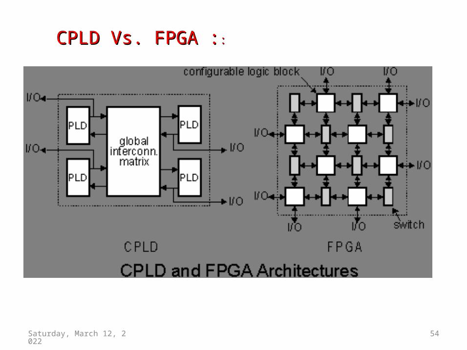
• Choosing Between CPLDs and FPGAs ::Choosing Between CPLDs and FPGAs ::
Friday, April 21, 2023 54
CPLD Vs. FPGA :CPLD Vs. FPGA :::

Friday, April 21, 2023 55
THANK YOUTHANK YOU


