132
EMT 396 Principles of IC Design (Prinsip-prinsip Rekabentuk Litar Terkamir LECTURER PN. NORINA BT. IDRIS TECHNICIAN PN. NOORSHAMIRA MUSTAFFA

EMT 396 Principles of IC Design (Prinsip-prinsip Rekabentuk Litar Terkamir
LECTURER
PN. NORINA BT. IDRIS
TECHNICIAN
PN. NOORSHAMIRA MUSTAFFA

• http://www.mediafire.com/?dzxc1s22d7hvgdg file name: 243introduction(2).rar password: ilovemalaysia
• Books: Weste and Rabaey
• http://www.downloadpdffree.com/CMOS-Digital-Integrated-Circuits-by-Sung-Mo-Kang-and-Yusuf-Leblebici.pdf

How to score …?

• First Day Materials\Engineering Your Future - Photonics Engineer.mp4
• SEcond Day Materials\Energy harvesting from the heart.mp4
4

• First Day Materials\Engineering Your Future - Photonics Engineer.mp4
5

Topics
• History
• Invention of transistors
• Transistor Types
• Moore’s Law & Outcomes
• Design versus Fabrication
• Effects of Scaling
• VLSI Design Styles
• ITRS
• Latest Technology Trends 6

Brief History
Bardeen, Shockley, and Brattain at
Bell Labs - Brattain and Bardeen
invented the bipolar transistor in
1947.
The first germanium bipolar
transistor. Roughly 50 years later,
electronics account for 10% (4
trillion dollars) of the world GDP.
It can be said that the invention of the transistor and the subsequent
development of the microelectronics have done more to shape the modern era
than any other invention.
The Start of the Modern Electronics Era
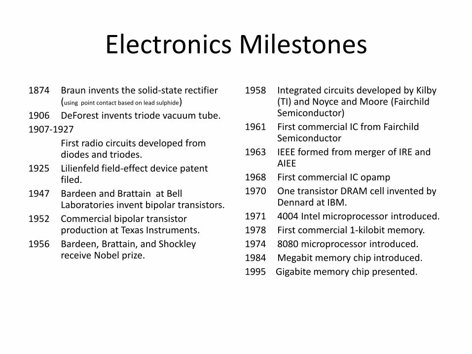
Electronics Milestones
1874 Braun invents the solid-state rectifier (using point contact based on lead sulphide)
1906 DeForest invents triode vacuum tube.
1907-1927
First radio circuits developed from diodes and triodes.
1925 Lilienfeld field-effect device patent filed.
1947 Bardeen and Brattain at Bell Laboratories invent bipolar transistors.
1952 Commercial bipolar transistor production at Texas Instruments.
1956 Bardeen, Brattain, and Shockley receive Nobel prize.
1958 Integrated circuits developed by Kilby (TI) and Noyce and Moore (Fairchild Semiconductor)
1961 First commercial IC from Fairchild Semiconductor
1963 IEEE formed from merger of IRE and AIEE
1968 First commercial IC opamp
1970 One transistor DRAM cell invented by Dennard at IBM.
1971 4004 Intel microprocessor introduced.
1978 First commercial 1-kilobit memory.
1974 8080 microprocessor introduced.
1984 Megabit memory chip introduced.
1995 Gigabite memory chip presented.

Evolution of Electronic Devices
Vacuum
Tubes
Discrete
Transistors
SSI and MSI
Integrated
Circuits
VLSI
Surface-Mount
Circuits

10

CHIPS ARE JUST ROCKS
The base material of a chip is usually silicon, although
materials such as sapphire and gallium arsenide are also
used. Silicon is found in quartz rocks and is purified in a
molten state. It is then chemically combined (doped) with
other materials to alter its electrical properties. The result
is a silicon crystal ingot up to 12 inches in diameter that is
either positively (p-type) or negatively charged (n-type).
Slices of the ingot approximately 1/30th of an inch thick
are cut from this "crystal salami." The slices are called
"wafers."
Silicon, the principal ingredient in
beach sand, is a natural
semiconductor and the most
abundant element on Earth except
for oxygen.

Driving all forms of digital innovation
Intel chips power Ultrabook™ devices, smartphones,
tablets, high performance computing, data centers,
and the Internet. They automate factories and are
embedded in automobiles and everyday devices.
The most sophisticated processor can contain
hundreds of millions or billions of transistors
interconnected by fine wires made of copper. Each
of these transistors acts as an on/off switch,
controlling the flow of electricity through the chip to
send, receive, and process information. Chips today
may have multiple cores.


• ..\..\downloads\Lecture 1\IntelProcessorHistory.pdf
• ..\..\downloads\Lecture 1\museum-transistors-to-transformations-brochure.pdf
• http://www.intel.com/content/www/us/en/company-overview/intel-museum.html
• ..\..\downloads\Lecture 1\history-moores-law-fun-facts-factsheet.pdf
17

Some Introduction
18

ICs ..what is it?
• ICs = Integrated Circuits
• A type of circuit in which thousands or millions or billions of components (transistors, resistors, capacitors) are integrated onto a single chip of semiconductive material of a very small size.
• Can be digital IC or analog IC or mixed-signals IC.
• Used in nearly all electronic equipments, such as: microprocessor, handphone, i-pad, microcontroller, memory, BIOS, etc.
• “Finger-tip” technology 19

VLSI Applications
• VLSI is an implementation technology for electronic circuitry - analogue or digital
• It is concerned with forming a pattern of interconnected switches and gates on the surface of a crystal of semiconductor
• Microprocessors
– personal computers
– microcontrollers
• Memory - DRAM / SRAM
• Special Purpose Processors - ASICS (CD players, DSP applications)
• Optical Switches
• Has made highly sophisticated control systems mass-producable and therefore cheap
20

Origins of VLSI ..1/2
• Much development motivated by WWII need for improved electronics, especially for radar
• 1940 - Russell Ohl (Bell Laboratories) - first pn junction
• 1948 - Shockley, Bardeen, Brattain (Bell Laboratories) - first transistor
– 1956 Nobel Physics Prize
• Late 1950s - purification of Si advances to acceptable levels for use in electronics
• 1958 - Seymour Cray (Control Data Corporation) - first transistorized computer - CDC 1604
21

Origins of VLSI …2/2
• 1959 - Jack St. Claire Kilby (Texas Instruments) - first integrated circuit - 10 components on 9 mm2
• 1959 - Robert Norton Noyce (founder, Fairchild Semiconductor) - improved integrated circuit
• 1968 - Noyce, Gordon E. Moore found Intel
• 1971 - Ted Hoff (Intel) - first microprocessor (4004) - 2300 transistors on 9 mm2
• Since then - continued improvement in technology has allowed for increased performance as predicted by Moore’s Law
22

WHAT IS IC?
ICs on PCB
IC Package
Inside IC Wafer 23

What is a Silicon Chip?
• A pattern of interconnected switches and gates on the surface of a crystal of semiconductor (typically Si)
• These switches and gates are made of
– areas of n-type silicon
– areas of p-type silicon
– areas of insulator
– lines of conductor (interconnects) joining areas together
• Aluminium, Copper, Titanium, Molybdenum, polysilicon, tungsten
• The geometryof these areas is known as the layout of the chip
• Connections from the chip to the outside world are made around the edge of the chip to facilitate connections to other devices
24

25

Wafer versus Die
26

THE ComPuTer Development
27

The 1st computer (1946)
28

29

Personal Computer The 60’s point of view
30

Scientific calculator 60’s design
31

WhaT’s inSiDe THE ComPuTer?
32
capacitors
M1
M2
TiN
passivation

Evolution in IC design
• 1966
• 1st IC circuit
• Motorola
• Consist of 3 input transistor
33

34

Intel 4004 • Introduction date:
November 15, 1971
• Clock speed: 108 KHz
• Number of transistors: 2,300 (10 microns)
• Bus width: 4 bits
• Addressable memory: 640 bytes
• Typical use: calculator, first microcomputer chip, arithmetic manipulation
35

Gallery - Early Processors
36
Mos Technology
6502 Intel 4004
First µP - 2300 xtors
L=10µm

37

Gallery - Current Processors
38
PowerPC 7400 (G4) 6.5M transistors / 450MHz / 8-10W
L=0.15µm
Pentium® III 28M transistors / 733MHz-1Gz / 13-26W
L=0.25µm shrunk to L=0.18µm

Gallery - Current Processors
39
Pentium® 4 42M transistors / 1.3-1.8GHz / 49-55W
L=0.18µm
Pentium® 4 “Northwood” 55M transistors / 2-2.5GHz
L=0.13µm

Pentium 4 • 0.18-micron process technology
(2, 1.9, 1.8, 1.7, 1.6, 1.5, and 1.4 GHz)
– Introduction date: August 27, 2001 (2, 1.9 GHz); ...; November 20, 2000 (1.5, 1.4 GHz)
– Level Two cache: 256 KB Advanced Transfer Cache (Integrated)
– System Bus Speed: 400 MHz
– SSE2 SIMD Extensions
– Transistors: 42 Million
– Typical Use: Desktops and entry-level workstations
• 0.13-micron process technology (2.53, 2.2, 2 GHz)
– Introduction date: January 7, 2002
– Level Two cache: 512 KB Advanced
– Transistors: 55 Million
40

Intel’s McKinley • Introduction date: Mid 2002
• Caches: 32KB L1, 256 KB L2, 3MB L3 (on-chip)
• Clock: 1GHz
• Transistors: 221 Million
• Area: 464mm2
• Typical Use: High-end servers
• Future versions: 5GHz, 0.13-micron technology
41

Gallery - Graphics Processor
42
nVidia GeForce4 57M transistors / 300MHz / ??W
L=0.15µm

Why Make ICs
• Integration improves:
– Size (much smaller than..)
– Speed (________er due to lower parasitics)
– Power (________er power consumption)
• Integration reduce manufacturing costs
– (almost) no manual assembly
• Money, technology, civilization
43

44
Trends in VLSI Technology
• Transistor
– Smaller, faster, use less power
• Number of transistors per chip
– Getting more
• Interconnect
– Less resistive, faster, longer (denser design)
• Yield
– Smaller die size, higher yield

Ref: http://micro.magnet.fsu.edu/creatures/technical/sizematters.html
• Modern transistors are few microns wide and approximately
0.1 micron or less in length
• Human hair is 80-90 microns in diameter
45

Digital ICs
• Many transistors (gates) fabricated onto one single chip.
• Current trend:
– Very Large Scale Integration (VLSI)
– Complementary Metal Oxide Semiconductor (CMOS)
– Fast, cheap, “low-power” transistor circuits
46

IC Scales of Integration
1. Small-scale integrated circuits (SSI)
– 10 gates or less
2. Medium-scale integrated circuits (MSI)
– Less than 1,000 gates Counters
3. Large-scale integrated circuits (LSI)
– Up to 104 gates First microprocessors on the chip
4. Very large-scale integrated circuits (VLSI)
– More than 104 gates
– 64-bit microprocessors with cache memories, floating point arithmetic, etc.
47

Other Scales of Integration..
• ULSI
• GSI
48
To find out the number of transistors..

INTRODUCTON TO VLSI DESIGN
• Brief History - TTL (Transistor-Transistor logic).
First successful IC logic family
Composed largest fraction of digital IC market until 80’s.
Power consumption per gate set upper limit on integration density.
- I2L (Integrated Injection Logic):
An attempt to provide a high integration density, low power bipolar
family of logic.
- MOS (Metal-Oxide-Silicon): Actually, we use polysilicon for gates now.
- PMOS-only used through early 70’s.
- In 1974, the 8080 microprocessor was implemented using faster NMOS only.
- Late 70’s, NMOS-only started suffering from same problem as high density
bipolar technology -- power consumption.
- CMOS was first !
Complexity of manufacturing process delayed use until 80’s.
Since early 80’s, CMOS remains the technology of choice.
However, power consumption is now becoming a problem.
And there is no new technology around the corner to alleviate the problem.
49

50
Evolution of IC Technologies ..1/2
• Bipolar technology
– TTL (transistor-transistor logic)
– ECL (emitter-coupled logic)
– I2L (Integrated Injection Logic)
• MOS (Metal-oxide-silicon)
– PMOS-only used through early 70’s.
– In 1974, the 8080 microprocessor was implemented using faster NMOS only.
– nMOS (n-channel MOS) technology developed in 1970s required fewer masking steps, was denser, and consumed less power than equivalent bipolar ICs => an MOS IC was cheaper than a bipolar IC and led to investment and growth of the MOS IC market.

51
Evolution of IC Technologies ..2/2
– aluminum for gates replaced by polysilicon by early 1980
– CMOS (Complementary MOS): n-channel and p-channel MOS transistors => lower power consumption, simplified fabrication process
• Bi-CMOS - hybrid Bipolar, CMOS (for high speed and low power consumption)
• GaAs - Gallium Arsenide (for high speed)
• Si-Ge - Silicon Germanium (for RF)

A Brief History
Invention of the Transistor
Vacuum tubes ruled in first half of 20th century Large, expensive, power-hungry, unreliable
1947: first point contact transistor (3 terminal devices)
Shockley, Bardeen and Brattain at Bell Labs
52

A Brief History, contd..
1958: First integrated circuit Flip-flop using two transistors
Built by Jack Kilby (Nobel Laureate) at Texas Instruments
Robert Noyce (Fairchild) is also considered as a co-inventor
smithsonianchips.si.edu/ augarten/
Kilby’s IC
53
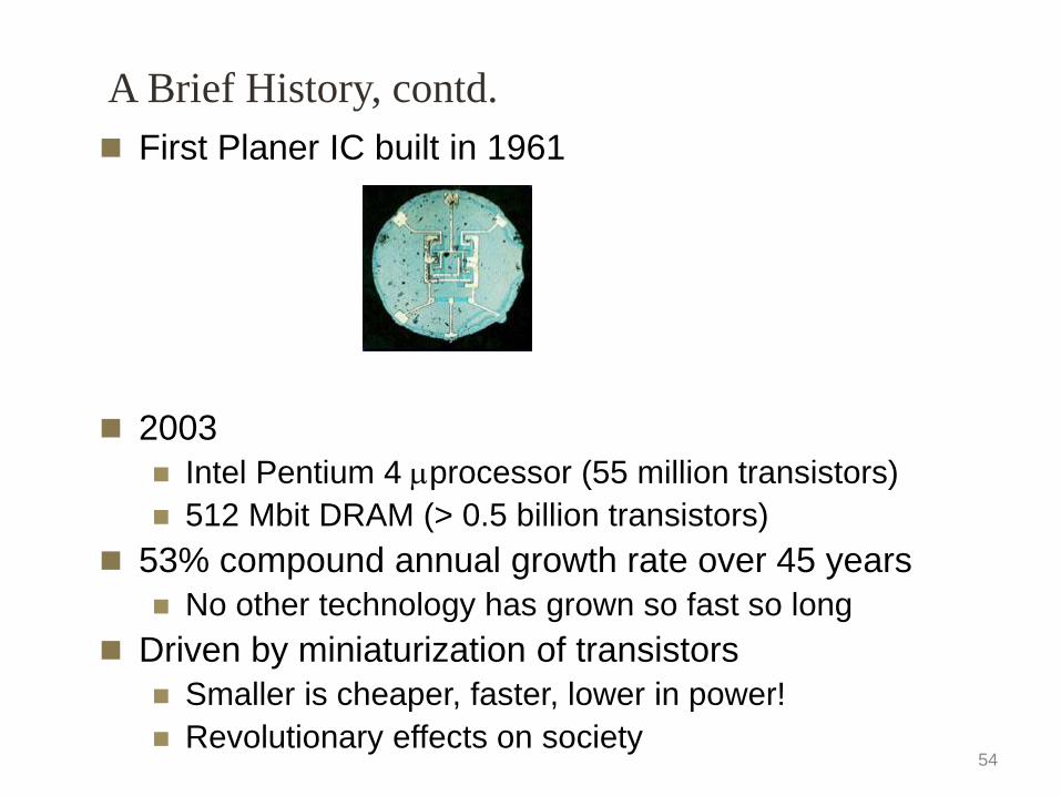
A Brief History, contd.
First Planer IC built in 1961
2003
Intel Pentium 4 processor (55 million transistors)
512 Mbit DRAM (> 0.5 billion transistors)
53% compound annual growth rate over 45 years
No other technology has grown so fast so long
Driven by miniaturization of transistors
Smaller is cheaper, faster, lower in power!
Revolutionary effects on society 54

Transistor Types
Bipolar transistors
npn or pnp silicon structure
Small current into very thin base layer controls large
currents between emitter and collector
Base currents limit integration density
Metal Oxide Semiconductor Field Effect Transistors
nMOS and pMOS MOSFETS
Voltage applied to insulated gate controls current
between source and drain
Low power allows very high integration
First patent in the ’20s in USA and Germany
Not widely used until the ’60s or ’70s
55

1970’s processes usually had only nMOS transistors Inexpensive, but consume power while idle
1980s-present: CMOS processes for low idle power
MOS Integrated Circuits
Intel 1101 256-bit SRAM Intel 4004 4-bit Proc
56

57
VLSI Technology - CMOS Transistors
Key feature:
transistor length L
2002: L=130nm
2003: L=90nm
2005: L=65nm?

Gordon Moore
58
I’m smiling
because I
was right!

Gordon Moore’s Evaluation & Prediction
• 1965 - observed trends in industry - # of transistors on ICs vs. release dates:
– Number of transistors doubling with release of each new IC generation
– Release dates (separate generations) were all 18-24 months apart
• Moore’s Law:
– The number of transistors on an integrated circuit would double every 18 months
• This comes about in two ways – size reduction of the individual
devices and increase in the chip or dice size
• Semiconductor industry has followed this prediction with surprising accuracy
59

How true..?
• 1965: Approximately 60 devices on a chip
• Proving Moore's law to be rather accurate, four decades later,
– Intel placed 1.7 billion transistors on its Itanium chip
• Both transistor density and IC performance has approximately DOUBLED every 18-24 months
60

Outcomes of Moore’s Law
• Many other factors also grow exponentially
• Data density doubles every 18-24 months (current definition of Moore’s Law)
•
61

Outcomes of Moore’s Law
– Transistor Density
Source: Intel web page (www.intel.com) 62
• From Intel’s 4040 (2300 transistors) to
• Pentium II (7,500,000 transistors) and beyond

Outcomes of Moore’s Law - Die Size
Relative sizes of ICs in graph
63

64
Outcomes of Moore’s Law -Data Density Growth

Outcomes of Moore’s Law
- Clock Speed Many other factors grow exponentially
Ex: clock frequency, processor performance
Year
1
10
100
1,000
10,000
1970 1975 1980 1985 1990 1995 2000 2005
4004
8008
8080
8086
80286
Intel386
Intel486
Pentium
Pentium Pro/II/III
Pentium 4
Clo
ck Speed (M
Hz)
65

Outcomes of Moore’s Law - Lower Cost per Transistor
66

Significant Breakthroughs Transistor size: Intel’s research labs have recently shown the world’s
smallest transistor, with a gate length of 15nm. We continue to build smaller
and smaller transistors that are faster and faster. We've reduced the size
from 70 nanometer to 30 nanometer to 20 nanometer, and now to 15
nanometer gates.
Manufacturing process: A new manufacturing process called 130 nanometer
process technology (a nanometer is a billionth of a meter) allows Intel today to
manufacture chips with circuitry so small it would take almost 1,000 of these
"wires" placed side-by-side to equal the width of a human hair. This new 130-
nanometer process has 60nm gate-length transistors and six layers of copper
interconnect. This process is producing microprocessors today with millions of
transistors and running at multi-gigahertz clock speeds.
Wafer size: Wafers, which are round polished disks made of silicon, provide
the base on which chips are manufactured. Use a bigger wafer and you can
reduce manufacturing costs. Intel has begun using a 300 millimeter (about 12
inches) diameter silicon wafer size, up from the previous wafer size of 200mm
(about 8 inches).
67

• ..\movies\What is Moore's Law-.mp4
68

69
Outcomes of Moore’s Law - Scaling
• The process of shrinking the layout in which every dimension is reduced by a factor is called Scaling.
• Transistors become cheaper, smaller, less resistive, switch faster, dissipate less power while at the same time, use less power.
• Designs have smaller die sizes, higher yield and increased performance.

Transistor Size Scaling
MOSFET performance
improves as size is
decreased:
shorter switching time,
lower power
consumption.
2 orders of magnitude reduction in transistor size in 30 years. 70

71
Can Scaling Continue? ..1/2
• Scaling work well in the past:
• In order to keep scaling work in the future, many technical problems and design challenges need to be solved.
Year 1989 1992 1995 1997 1999
Technology
(m) 0.65 0.5 0.35 0.25 0.18
2001
0.15

72
Can Scaling Continue? ..2/2
• Some characteristics of the transistors do not scale uniformly, e.g., delay, leakage current, threshold voltage, etc.
• Mismatch in the scaling of transistors and interconnects. Interconnect delay has increased from 5-10% of the overall delay to 50-70%.
TSMC 0.15 CMOS Technology

ITRS – International Technology Roadmap for Semiconductors
73

74
Technology Directions: SIA Roadmap
Year 1999 2002 2005 2008 2011 2014 Feature size (nm) 180 130 100 70 50 35
Logic trans/cm2 6.2M 18M 39M 84M 180M 390M
Cost/trans (mc) 1.735 .580 .255 .110 .049 .022
#pads/chip 1867 2553 3492 4776 6532 8935
Clock (MHz) 1250 2100 3500 6000 10000 16900
Chip size (mm2) 340 430 520 620 750 900
Wiring levels 6-7 7 7-8 8-9 9 10
Power supply (V) 1.8 1.5 1.2 0.9 0.6 0.5
High-perf pow (W) 90 130 160 170 175 183

Limits of Moore’s Law?
• Growth expected until 30 nm gate length (currently: 180 nm)
– size halved every 18 mos. - reached in
2001 + 1.5 log2((180/30)2) = 2009
– what then?
• But, is the end is in sight?
– Physical limitations
– Economic limitations
• Paradigm shift needed in fabrication process
75
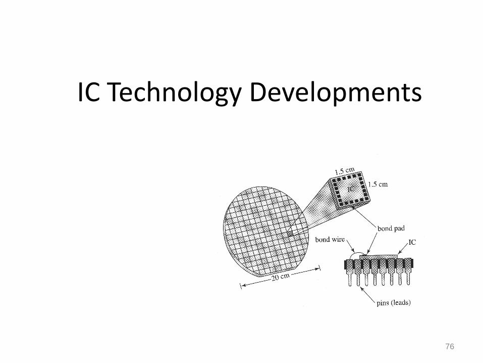
IC Technology Developments
76

77
Microprocessor Trends (Log Scale)
Sources: http://www.intel.com/pressroom/kits/quickreffam.htm, www.geek.com
0.001
0.01
0.1
1
10
100
1970 1975 1980 1985 1990 1995 2000 2005
Tra
nsis
tors
(M
illi
on
s)
Intel
Motorola
DEC/Compaq
Alpha (R.I.P)
P4N
G4
P4

Die Size Growth
4004 8008
8080 8085
8086 286
386 486 Pentium ® proc
P6
1
10
100
1970 1980 1990 2000 2010
Year
Die
siz
e (
mm
)
~7% growth per year
~2X growth in 10 years
Die size grows by 14% to satisfy Moore’s Law
Courtesy, Intel 78

Frequency Improvements
79

80
Microprocessor Trends (Intel)
Year Chip L transistors
1971 4004 10µm 2.3K
1974 8080 6µm 6.0K
1976 8088 3µm 29K
1982 80286 1.5µm 134K
1985 80386 1.5µm 275K
1989 80486 0.8µm 1.2M
1993 Pentium® 0.8µm 3.1M
1995 Pentium® Pro 0.6µm 15.5M
1999 Mobile PII 0.25µm 27.4
2000 Pentium® 4 0.18µm 42M
2002 Pentium® 4 (N) 0.13µm 55M
Source: http://www.intel.com/pressroom/kits/quickreffam.htm

81

Evolution of Memory
82

83
DRAM Memory Trends (Log Scale)
Source: Textbook, Industry Reports
0.0625
0.25
1
4
16
64128
256512
0.01
0.1
1
10
100
1000
1975 1980 1985 1990 1995 2000 2005
Size (Mb)

Evolution of Lithography
84

85
Summary - Technology Trends
• Processor
– Logic capacity increases ~ 30% per year
– Clock frequency increases ~ 20% per year
– Cost per function decreases ~20% per year
• Memory
– DRAM capacity: increases ~ 60% per year (4x every 3 years)
– Speed: increases ~ 10% per year
– Cost per bit: decreases ~25% per year

86
These trends have brought many changes and new challenges to
circuit design.

87
Complicated Design
• Too many transistors and no way to handle them manually.
• Solutions:
– CAD
– Hierarchical design
– Design re-use

88
Power and Noise
• Huge power consumption and heat dissipation becomes a problem
• Noise and cross talk.
• Solutions:
– Better physical design

89
Interconnect Area
• Too many interconnects
• Solutions:
– More interconnect layers (made possible by Chemical-Mechanical Polishing)
– CAD tools for 3-D routing

Major Design Challenges • Microscopic issues
– ultra-high speeds
– power dissipation and supply rail drop
– growing importance of interconnect
– noise, crosstalk
– reliability, manufacturability
– clock distribution
• Macroscopic issues
– time-to-market
– design complexity (millions of gates)
– high levels of abstractions
– design for test
– reuse and IP, portability
– systems on a chip (SoC)
– tool interoperability
Year Tech. Complexity Frequency Staff Size Staff Costs
1997 0.35 13 M Tr. 400 MHz 210 $90 M
1998 0.25 20 M Tr. 500 MHz 270 $120 M
1999 0.18 32 M Tr. 600 MHz 360 $160 M
2002 0.13 130 M Tr. 800 MHz 800 $360 M
90

Design Styles
91

92
Silicon Manufacturing Alternatives
Standard Components Application Specific ICs
Fixed
Application
Application
by Programming
Semi
Custom
Silicon
Compilation
Full
Custom
Logic Families
Hardware Programming
(MASK)
Software
Programming
TTL
CMOS
PLA
ROM Microprocessor
EPROM,EEPROM PLD, FPGA

93
SOC.. Goes where?

Full Custom Design
• Each circuit element carefully “handcrafted”
• Huge design effort
• High Design & NRE Costs / Low Unit Cost
• High Performance
• Typically used for high-volume applications
94

Application-Specific Integrated Circuit (ASIC)
• Constrained design using pre-designed (and sometimes pre-manufactured) components
• Also called semi-custom design
• CAD tools greatly reduce design effort
• Low Design Cost / High NRE Cost / Med. Unit Cost
• Medium Performance
95

Programmable Logic (PLDs, FPGAs)
• Pre-manufactured components with programmable interconnect
• CAD tools greatly reduce design effort
• Low Design Cost / Low NRE Cost / High Unit Cost
• Lower Performance
96

積體電路實驗室
逢甲大學電子工程研究所2013/2/22 FCUECE_DGL_VLSI 17
Design Technology
晶片佈局
佈局
包裝
晶圓製造
晶片切割
印刷電路板組裝及測試
97 Adapted from original source…

98

System-on-a-chip (SOC)
• Idea: combine several large blocks – Predesigned custom cores (e.g., microcontroller) -
“intellectual property” (IP)
– ASIC logic for special-purpose hardware
– Programmable Logic (PLD, FPGA)
– Analog
• Open issues – Keeping design cost low
– Verifying correctness of design
99

Perspective on Design Styles
• Few engineers will design custom chips
• Some engineers will design ASICs & SOCs
• Many engineers will design FPGA systems
100

101

3-D VLSI
• The fabrication of a single integrated circuit whose functional parts (transistors, etc) extend in three dimensions
• The vertical orientation of several bare integrated circuits in a single package
102

Advantages of 3D VLSI 1/5
• Speed - the time required for a signal to travel between the functional circuit blocks in a system (delay) reduced.
– Delay depends on resistance/capacitance of interconnections
– resistance proportional to interconnection length
103

Advantages of 3D VLSI …2/5
• Noise - unwanted disturbances on a useful signal – reflection noise (varying impedance along interconnect)
– crosstalk noise (interference between interconnects)
– electromagnetic interference (EMI) (caused by current in pins)
• 3D chips – fewer, shorter interconnects
– fewer pins
104

Advantages of 3D VLSI …3/5
• Power consumption
– power used charging an interconnect capacitance
• P = fCV2 – power dissipated through resistive material
• P = V2/R – capacitance/resistance proportional to length
– reduced interconnect lengths will reduce power
105

Advantages of 3D VLSI …4/5
• Interconnect capacity (connectivity)
– more connections between chips
– increased functionality, ease of design
106

Advantages of 3D VLSI …5/5
• Printed circuit board size/weight
– planar size of PCB reduced with negligible IC height increase
– weight reduction due to more circuitry per package/smaller PCBs
– estimated 40-50 times reduction in size/weight
107

3D VLSI - Challenges and Solutions
• Challenge: Thermal management
– smaller packages
– increased circuit density
– increased power density
• Solutions:
– circuit layout (design stage)
• high power sections uniformly distributed
– advancement in cooling techniques (heat pipes)
108

Influential Participants - Industry
• Mitsubishi, TI, Intel, CTS Microelectronics, Hitachi, Irvine Sensors, others...
– high density memories
• AT&T
– high density “multiprocessor”
• Many other applications/participants
109

3D VLSI
• Moore’s Law approaching physical limit
• Increased performance expected by market
• Paradigm shift needed - 3D VLSI
– many advantages over 2D VLSI
– economic limitations of fabrication overhaul will be overcome by market demand
• Three Dimensional VLSI may be the savior of Moore’s Law
110

Chip Application
111

112

113

114

115

116

Fully Depleted Transistor (FDT) & 28 nm Technology (and smaller)
• ..\..\downloads\Lecture 1\Fully depleted silicon technology to underlie energy.docx
117

• ..\movies\Moore's Law and The Secret World Of Ones And Zeroes.mp4
118


IOT
• The “Internet of things” (IoT) is becoming an increasingly growing topic of conversation both in the workplace and outside of it. It’s a concept that not only has the potential to impact how we live but also how we work.
• Broadband Internet is become more widely available, the cost of connecting is decreasing, more devices are being created with wifi capabilities and sensors built into them, technology costs are going down, and smart phone penetration is sky-rocketing.
• Simply put this is the concept of basically connecting any device with an on and off switch to the Internet (and/or to each other). This includes everything from cell phones, coffee makers, washing machines, headphones, lamps, wearable devices and almost anything else you can think of. This also applies to components of machines, for example a jet engine of an airplane or the drill of an oil rig.
• relationship will be between people-people, people-things, and things-things

• The reality is that the IoT allows for virtually endless opportunities and connections to take place, many of which we can’t even think of or fully understand the impact of today. It’s not hard to see how and why the IoT is such a hot topic today, it certainly opens the door to a lot of opportunities but also to many challenges. Security is big issues that is oftentimes brought up. With billions of devices being connect together what can people to do make sure that their information stays secure? Will someone be able to hack into your toaster and thereby get access to your entire network? The IoT also opens up companies all over the world to more security threats. Then we have the issue of privacy and data sharing.

122

Design Stages
• Hierarchical: Top- Down or Bottom-Up?
• Gate level -> Transistor level -> Layout
123

124

You WILL be GooD at tHiS..
125

And, in fuTuRe ..
126

To Search Tonight ..
IC Definitions
Latest trends of Moore’s law outcomes
Find more articles on latest technologies –
SAT, SET, 3D, 4D, and ..?
127

Words of wisdom
128
DON’T FORGET ABOUT WHAT YOU HAVE LEARNT!!!!!!!!!!!!!

State the year, by whom from which company.. State the number of transistors/gates inside that IC
• the fist IC was in introduced to the world
• the fist Intel IC was in introduced
129

Design House
130

Design -from schematics -from HDL
131

Fabrication (Fab) House
132


![index [portal.unimap.edu.my]portal.unimap.edu.my/portal/page/portal30/Lecture Notes...Programmable Logic Devices (PLDs) are ICs with a large number of gates and flip flops that can](https://static.documents.pub/doc/80x56/5e7054cbeb00c9419349ced3/index-notes-programmable-logic-devices-plds-are-ics-with-a-large-number.jpg)


