POLYMER ORGANIC SOLAR CELLS Phua Hao Yu A0086715X A THESIS SUBMITTED IN PARTIAL FULFILLMENT TOWARDS THE BACHELOR OF SCIENCE (HONORS) IN PHYSICS DEPARTMENT OF PHYSICS NATIONAL UNIVERSITY OF SINGAPORE 2015
Transcript
POLYMER ORGANIC SOLAR CELLS
Phua Hao Yu
A0086715X
A THESIS SUBMITTED IN PARTIAL FULFILLMENT TOWARDS
THE BACHELOR OF SCIENCE (HONORS) IN PHYSICS
DEPARTMENT OF PHYSICS
NATIONAL UNIVERSITY OF SINGAPORE
2015
ii
iii
Acknowledgements
I would like to thank A/Prof Peter Ho, Asst/Prof Chua Lay-Lay and Dr Rachael Png Ruiqi for
accommodating me in the Organic Nano Device Lab.
My heartfelt gratitude to Jun Kai for taking time to guide me in both theoretical and
experimental aspects of this study. For tolerating my shenanigans and not turning into a
disciplinarian, which turned out more for the better, while still giving out reprimands and
encouragements whenever necessary. Thank you for teaching me skills beyond the classroom
and for making the journey a pleasant one.
In the midst of this, we mourn the passing of Mr Lee Kuan Yew.
Thank you to Rachael for taking time out of her now even more busy schedule to review this
work.
And to the rest of ONDL for their guidance in times of trouble and aid that made this work
possible. I am appreciative of the warmth received from the members of ONDL and the
cleanroom.
I would also like to thank my family and friends for the support they provided.
iv
Abstract
Organic photovoltaics possess many qualities that are rarely available in inorganic
photovoltaics, namely its ability for high absorbance, flexibility, cheap and high throughput
processing. While electron donor polymers are many aplenty, electron acceptor polymers with
high electron mobility are just introduced to the stage and competes with fullerene derivatives
that has its long standing reputation as the acceptor material of choice. In the other corner,
morphology plays an important factor influencing PCE of an organic solar cell. Bulk
heterojunctions of organic solar cells are usually formed from spontaneously demixed biblends
of the active layer solution and removes control from the hands of the investigator. Many efforts
were made to wrestle control back but these still relied on the spontaneous demixing of the
solution. In this study, a crosslinked donor matrix structure is employed to create a controllable
morphology of donor polymers which is then filled and back-infiltrated with acceptor materials.
We demonstrate that a crosslinked back-infiltrated solar cell improve in performance over a
demixed biblend. However, this method showed some dependence on the donor material
involved, hence requires some tailoring for optimal adoption. Devices with small molecule
back-infiltrated sets the amount of infiltration that might optimally occur and were closely
matched by low molecular weight polymers but not by high molecular weight polymers. As
mobility is dependent on molecular weight, this balance is identified as one of the parameters
that requires optimising. Device parameter of Voc was observed to increase over all device
tested and this notable effect should be studied in greater detail and could lend to a clearer
picture of the morphology in a crosslinked back-infiltrated active layer.
v
Table of Contents
Acknowledgements .................................................................................................................. iii
Abstract ..................................................................................................................................... iv
Table of Contents ....................................................................................................................... v
Figure 24: a) Linear-linear J-V curve of PBDTTPD:PNDI HMW demixed biblend and back-
infiltrated and PBDTTPD:PNDI 30k back-infiltrated device . b) Log-linear J-V curve.
Table 4: Output parameters of devices. *Unadjusted data.
PCE (%) Voc (V) Jsc
(mAcm-2) Vmpp (V)
Jmpp (mAcm-2)
FF QE* (%)
PBDTTPD:PNDI HMW demixed biblend
0.963 0.809 3.866 0.460 2.093 0.308 93.2
PBDTTPD:PNDI HMW back-infiltrated
0.139 0.932 0.624 0.410 0.340 0.240 69.7
PBDTTPD:PNDI 30k back-infiltrated
0.012 0.530 0.098 0.280 0.042 0.224 83.1
Figure 24a shows us the poor performance of the back-infiltrated devices where parameters
fell in almost all except for some Voc. Similar to the previous PBDTTPD:PCBM devices,
PBDTTPD:PNDI devices showed poor FF. Jsc of the back-infiltrated device showed a drastic
reduction when compared with the demixed biblend. When taken into account the drop in
mobility of PBDTTPD after crosslinking, the Jsc was about 25% of that of demixed biblend.
This coincides well with the model of a bilayer where the effective active layer is only 20nm,
due to the short diffusion length of the exciton, when compared to the 100nm thick demixed
biblend.
31
However, PL of PBDTTPD:PNDI HMW back-infiltrated active layer was not significantly
lower than that of the demixed biblend, standing at 75% of the biblend’s quenching efficiency,
furthermore, QE was similar to PBDTTPD:PCBM in CB back-infiltrated active layer which
meant similar levels of infiltration. Comparison between these devices showed consistent lower
performance (PCE and FF) on part of the PNDI HMW polymer and would point the cause
towards the lower electron mobility of PNDI. Back-infiltration of the smaller molecular weight
polymer (PNDI 30k) once again showed higher QE over PNDI HMW.
In PBDTTPD demixed biblend, the QE reached near ideal levels which indicate a fine phase
separation for the donor material, while for the crosslinked system, use of a low molecular
weight PNDI or PCBM in CF also provided deep infiltration to lead QE near ideal levels.
However, FF for back-infiltrated device fell and this would point us to a conclusion of a coarser
phase separation in the acceptor domain.
3.3 Semiconducting behaviour of PNDI on molecular weight
Though the course of this study, it has been observed that the semiconducting behaviour of
PNDI had a dependence on molecular weight. Mobility of semicrystalline semiconducting
polymers are not entirely dependent on chain length for their mobility. This is especially true
for low molecular weight variants where processing conditions can modify their mobilities by
a hundred times29. As PNDI is shown to exhibit semicrystalline properties25, SCLC electron
mobility of PNDI are fit with a linear relationship to the molecular weight of the polymer to
provide a simple estimation on the mobility with its molecular weight. This will allow the
targeting of a certain molecular weight for the desired mobility, in order to improve infiltration.
32
10-7
10-5
10-3
10-1
101
103
105
-6 -4 -2 0 2 4 6
PNDI HMW
PNDI 30kPNDI 20k
Cur
rent
den
sity
(m
Acm
-2)
Voltage (V)
a)
0
5 10-9
1 10-8
1.5 10-8
2 10-8
2.5 10-8
3 10-8
3.5 10-8
4 10-8
0 50 100 150 200 250 300
y = -3.3694e-09 + 1.6858e-10x R= 0.99967
SC
LC e
lect
ron
mob
ility
m2/(
Vs)
Molecular Weight (kDa)
b)
Figure 25: a) J-V curve of PNDI HMW, 20k and 30k. b) Linear fit of SCLC electron mobility
against molecular weight.
3.4 Symmetricity
Symmetricity of mobilities between donor and acceptor materials have also to be taken into
account. Free charge carriers generated in the middle of the active layer, if met with an
asymmetric mobility between holes and electron, can lead to a build-up of charge carriers
within the active layer as the faster rate of extraction of a type of charge carrier leaves a net of
the opposite charge in the active layer. This space charge then impedes the flow of free charge
carriers, requiring a higher potential to fully extract charge carriers, hence mobilities of similar
orders are required for efficient extraction.
However, the generation of charge carriers are dependent on the absorption profile of the device
with the depth of the device, and because of the orientation of the device and the optical
interference from the reflected rays off the back of the device, an asymmetry is generated. In
an active layer where reflection is minimized, this would lead to a larger optical profile in the
front with the node at the back. Since the devices in this work are of superstrate structure, light
enters from the hole collection electrodes and this corresponds to a hole collection electrode
nearer to the bulk of the generated free charge carriers. As a result, electron have to travel a
much larger distance to reach their electrode, and to aid them in their travels, an acceptor
material with higher electron mobility should be deployed.
33
The optimal ratio for electron to hole mobility for superstrate structures was reported30 to be
around 10 (�7/�D ≈ 10), with parallel increases in mobility giving, intuitively, higher FF and
PCE. The massively low FF experienced by PBDTTPD:PNDI is within expectations of the
combined low mobilities of PBDTTPD and PNDI.
Donor polymers have SCLC hole mobilities in the typical range of 10�? to 10�� m2/(Vs),
hence optimal electron mobility would range from 10�� to 10�� m2/(Vs). Referring to figure
25, this would rule out the use of low molecular weight PNDIs below 100k molecular weight
as suitable acceptors for current donor polymers. However, PNDIs between 100-250k
molecular weight can be investigated for better infiltration while not sacrificing too much on
performance.
34
4. Conclusion
Overall, crosslinking has provided quite a useful tool in improving morphology and
performance of the solar cell. The drop in mobilities for crosslinked matrix was more than
compensated by the improvements in morphology. The larger hole mobility drop for
PBDTTPD crosslinked matrix only serves to provide an avenue for concocting a more suitable
crosslinker, which will further improve cell performance.
Phase separation of donor and acceptor domains is still less than ideal and can be optimized for
each specific active layer type, through adjustment of the extent of crosslinking in the donor
phase. In all cases of PNDI HMW back-infiltration, lower levels of infiltration were observed.
However, the drop was not enormous and optimising processing conditions is believed to be
able to improve cell performance.
There were mixed reactions towards Jsc and FF as these two parameters depend on many
factors, including morphology and mobilities. Voc followed trends according to their
theoretical limit but for crosslinked back-infiltrated devices, an increase in Voc across the
board was impressively observed but not understood. This increase is thought to be due to the
presence of a slight bilayer on top of the crosslinked matrix which might provide better
extraction of charge carriers with its larger cross-sectional area hence lower resistance.
Due to the optimal mobility ratio, it is expected that PNDI below 100k molecular weight would
produce less than spectacular results due to its low mobility, while PNDI between 100-250k
molecular weight should produce better infiltration without much loss in performance. Further
breakthroughs in high electron mobility polymers will provide great excitement in the field of
organic semiconductors where crosslinkers will still be able to aid in providing morphology
support.
35
5. References
1. Morris, I., Why the west rules-for now: The patterns of history and what they reveal about the future. Profile books: 2010. 2. Wirth, H., Recent facts about photovoltaics in Germany. Fraunhofer ISE: January 7 2015. 3. Chamberlain, G., Organic solar cells: a review. Solar cells 1983, 8 (1), 47-83. 4. Lizin, S.; Van Passel, S.; De Schepper, E.; Maes, W.; Lutsen, L.; Manca, J.; Vanderzande, D., Life cycle analyses of organic photovoltaics: a review. Energy & Environmental Science 2013, 6 (11), 3136-3149. 5. Forrest, S. R., The path to ubiquitous and low-cost organic electronic appliances on plastic. Nature 2004, 428 (6986), 911-918. 6. Brédas, J.-L.; Beljonne, D.; Coropceanu, V.; Cornil, J., Charge-transfer and energy-transfer processes in π-conjugated oligomers and polymers: a molecular picture. Chemical Reviews 2004, 104 (11), 4971-5004. 7. Peumans, P.; Uchida, S.; Forrest, S. R., Efficient bulk heterojunction photovoltaic cells using small-molecular-weight organic thin films. Nature 2003, 425 (6954), 158-162. 8. Brabec, C. J.; Zerza, G.; Cerullo, G.; De Silvestri, S.; Luzzati, S.; Hummelen, J. C.; Sariciftci, S., Tracing photoinduced electron transfer process in conjugated polymer/fullerene bulk heterojunctions in real time. Chemical Physics Letters 2001, 340 (3), 232-236. 9. Tang, C. W., Two‐layer organic photovoltaic cell. Applied Physics Letters 1986, 48 (2), 183-185. 10. Yu, G.; Gao, J.; Hummelen, J. C.; Wudl, F.; Heeger, A. J., Polymer photovoltaic cells: enhanced efficiencies via a network of internal donor-acceptor heterojunctions. Science-AAAS-Weekly Paper Edition 1995, 270 (5243), 1789-1790. 11. Chi, D.; Qu, S.; Wang, Z.; Wang, J., High efficiency P3HT: PCBM solar cells with an inserted PCBM layer. Journal of Materials Chemistry C 2014, 2 (22), 4383-4387. 12. Png, R.-Q.; Chia, P.-J.; Tang, J.-C.; Liu, B.; Sivaramakrishnan, S.; Zhou, M.; Khong, S.-H.; Chan, H. S.; Burroughes, J. H.; Chua, L.-L., High-performance polymer semiconducting heterostructure devices by nitrene-mediated photocrosslinking of alkyl side chains. Nature materials 2010, 9 (2), 152-158. 13. Liu, B.; Png, R.-Q.; Zhao, L.-H.; Chua, L.-L.; Friend, R. H.; Ho, P. K., High internal quantum efficiency in fullerene solar cells based on crosslinked polymer donor networks. Nature communications 2012, 3, 1321. 14. Garcia-Belmonte, G.; Munar, A.; Barea, E. M.; Bisquert, J.; Ugarte, I.; Pacios, R., Charge carrier mobility and lifetime of organic bulk heterojunctions analyzed by impedance spectroscopy. Organic Electronics 2008, 9 (5), 847-851. 15. Dang, M. T.; Hirsch, L.; Wantz, G., P3HT: PCBM, best seller in polymer photovoltaic research. Advanced Materials 2011, 23 (31), 3597-3602. 16. Yan, H.; Chen, Z.; Zheng, Y.; Newman, C.; Quinn, J. R.; Dötz, F.; Kastler, M.; Facchetti, A., A high-mobility electron-transporting polymer for printed transistors. Nature 2009, 457 (7230), 679-686. 17. Zou, Y.; Najari, A.; Berrouard, P.; Beaupré, S.; Réda Aïch, B.; Tao, Y.; Leclerc, M.,
A thieno [3, 4-c] pyrrole-4, 6-dione-based copolymer for efficient solar cells. Journal of the American Chemical Society 2010, 132 (15), 5330-5331. 18. Qin, R.; Li, W.; Li, C.; Du, C.; Veit, C.; Schleiermacher, H.-F.; Andersson, M.; Bo, Z.; Liu, Z.; Inganas, O., A planar copolymer for high efficiency polymer solar cells. Journal of the American Chemical Society 2009, 131 (41), 14612-14613. 19. Oriel® Sol2A™ Class ABA Solar Simulators. Newport: 2007.
36
20. de Mello, J. C.; Wittmann, H. F.; Friend, R. H., An improved experimental determination of external photoluminescence quantum efficiency. Advanced materials 1997, 9 (3), 230-232. 21. Dennler, G.; Scharber, M. C.; Brabec, C. J., Polymer‐Fullerene bulk‐heterojunction solar cells. Advanced Materials 2009, 21 (13), 1323-1338. 22. Yang, X.; Loos, J.; Veenstra, S. C.; Verhees, W. J.; Wienk, M. M.; Kroon, J. M.; Michels, M. A.; Janssen, R. A., Nanoscale morphology of high-performance polymer solar cells. Nano letters 2005, 5 (4), 579-583. 23. Tremolet de Villers, B.; Tassone, C. J.; Tolbert, S. H.; Schwartz, B. J., Improving the reproducibility of P3HT: PCBM solar cells by controlling the PCBM/cathode interface. The Journal of Physical Chemistry C 2009, 113 (44), 18978-18982. 24. Liu, Z.; Lee, E.-C., Efficiency improvement in fullerene-layer-inserted organic bulk-heterojunction solar cells. Journal of Applied Physics 2012, 111 (2), 023104. 25. Schubert, M.; Dolfen, D.; Frisch, J.; Roland, S.; Steyrleuthner, R.; Stiller, B.; Chen, Z.; Scherf, U.; Koch, N.; Facchetti, A., Influence of Aggregation on the Performance of All‐Polymer Solar Cells Containing Low‐Bandgap Naphthalenediimide Copolymers. Advanced Energy Materials 2012, 2 (3), 369-380. 26. Zhou, N.; Lin, H.; Lou, S. J.; Yu, X.; Guo, P.; Manley, E. F.; Loser, S.; Hartnett, P.; Huang, H.; Wasielewski, M. R., Morphology‐Performance Relationships in High‐Efficiency All‐Polymer Solar Cells. Advanced Energy Materials 2014, 4 (3). 27. Aïch, B. R.; Lu, J.; Beaupré, S.; Leclerc, M.; Tao, Y., Control of the active layer nanomorphology by using co-additives towards high-performance bulk heterojunction solar cells. Organic Electronics 2012, 13 (9), 1736-1741. 28. Kronholm, D.; Hummelen, J., Fullerene-based n-type semiconductors in organic electronics. Material Matters 2007, 2, 16-20. 29. Kline, R. J.; McGehee, M. D.; Kadnikova, E. N.; Liu, J.; Frechet, J. M.; Toney, M. F., Dependence of regioregular poly (3-hexylthiophene) film morphology and field-effect mobility on molecular weight. Macromolecules 2005, 38 (8), 3312-3319. 30. Liu, B.; Png, R. Q.; Tan, J. K.; Ho, P. K., Evaluation of Built‐In Potential and Loss Mechanisms at Contacts in Organic Solar Cells: Device Model Parameterization, Validation, and Prediction. Advanced Energy Materials 2014, 4 (4).
37
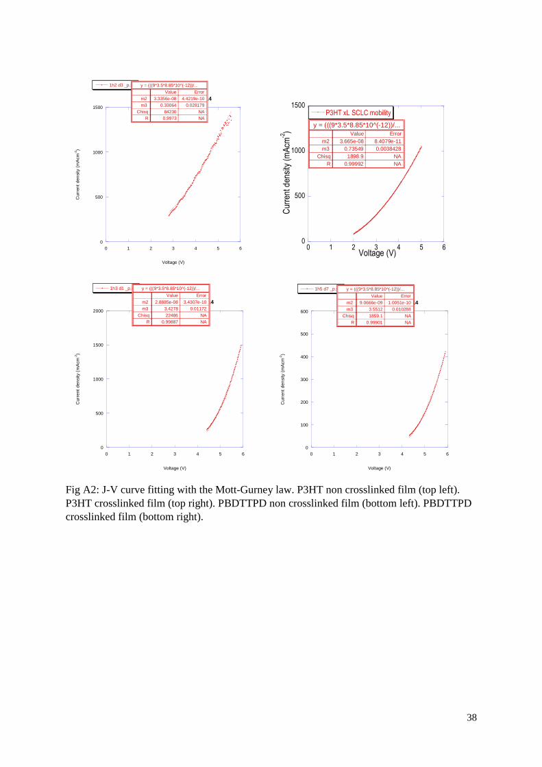
6. Appendix
A1. SCLC mobility
10-6
10-4
10-2
100
102
104
-6 -4 -2 0 2 4 6
P3HT no crosslinkP3HT with crosslinkPBDTTPB no crosslinkPBDTTPB with crosslink
Cur
rent
den
sity
(m
Acm
-2)
Voltage (V)
Fig A1: J-V curves of P3HT and PBDTTPD non crosslinked and crosslinked films.
38
0
500
1000
1500
0 1 2 3 4 5 6
sheet1 12:46:14 PM 15/12/2014
1h2 d3 _p.xls
Cur
rent
den
sity
(m
Acm
-2)
Voltage (V)
y = (((9*3.5*8.85*10^(-12))/...
ErrorValue
4.4219e-103.3356e-08m2
0.0281790.33064m3
NA84230ChisqNA0.9973R
0
500
1000
1500
0 1 2 3 4 5 6
P3HT xL SCLC mobility
Cur
rent
den
sity
(m
Acm
-2)
Voltage (V)
y = (((9*3.5*8.85*10^(-12))/...ErrorValue
8.4079e-113.665e-08m2 0.00384280.73549m3
NA1898.9ChisqNA0.99992R
0
500
1000
1500
2000
0 1 2 3 4 5 6
sheet1 12:46:14 PM 15/12/2014
1h3 d1 _p.xls
Cur
rent
den
sity
(m
Acm
-2)
Voltage (V)
y = (((9*3.5*8.85*10^(-12))/...
ErrorValue
3.4307e-102.8885e-08m2 0.011723.4278m3
NA22486ChisqNA0.99887R
0
100
200
300
400
500
600
0 1 2 3 4 5 6
sheet1 12:46:14 PM 15/12/2014
1h5 d7 _p.xls
Cur
rent
den
sity
(m
Acm
-2)
Voltage (V)
y = (((9*3.5*8.85*10^(-12))/...
ErrorValue
1.0051e-109.0666e-09m2
0.0102883.5512m3
NA1859.1Chisq
NA0.99901R
Fig A2: J-V curve fitting with the Mott-Gurney law. P3HT non crosslinked film (top left). P3HT crosslinked film (top right). PBDTTPD non crosslinked film (bottom left). PBDTTPD crosslinked film (bottom right).