169
Polymers and biopolymers in micro- and nanotechnology Polymerscience Nanoscience Physics Chemistry Life Sciences Engineering Sciences
| Date post: | 28-Aug-2018 |
| Category: |
Documents |
| Upload: | trinhtuong |
| View: | 222 times |
| Download: | 0 times |

Polymers and biopolymers in
micro- and nanotechnology
PolymerscienceNanoscience
Physics Chemistry
Life Sciences Engineering Sciences
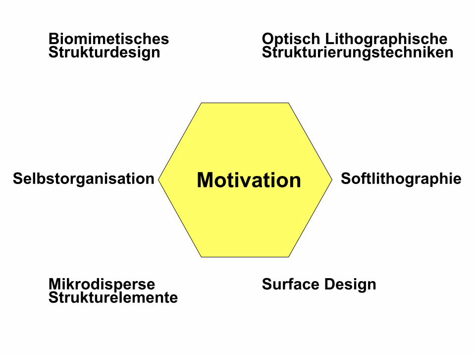
Optisch LithographischeStrukturierungstechniken
Softlithographie
Surface DesignMikrodisperseStrukturelemente
Selbstorganisation
BiomimetischesStrukturdesign
Motivation

Polymers and biopolymers in micro- and nanotechnology
What are micro- and nanotechnology about ?
• Majour goals • Representative examples from microtechnology• Representative examples from nanotechnology
What are the materials used in micro- and nanotechnology?
• Silicon, metals, semiconductors and inorganics• Polymers, organic materials

Polymers and biopolymers in micro- and nanotechnology
What are the technologies used in micro- and nanosciences?
• Structuring technologies• Analytical techniques• Self assembly
What is the biological input to micro- and nanotechnology?
• Biomimetic strategies• Biophysical techniques
What are the visionary goals of nanotechnology ?

Goals of nanotechnology
Nanotechnology focuses on
• preparation • analysis • understanding of physical properties and • technological application
of nano- and mesosized objects

Nanoobjects
1-d 2-d 3-d
yy
xy
xz
< 100 nm
Layers Rods Particles

History of nanotechnology
Ultrathin gold layers ( 100 nm)

History of nanotechnology
Technological applications of nanoobjects
Colloidal colours in glases –Optical properties of nanoparticles

History of nanotechnology
Alchemist Kunckel
1682
Johann Kunckel, der am sächsischen Hof diente und sich in der europäischen Glaskunst auskannte, wurde vom Großen Kurfürsten um 1678 nach Brandenburg gerufen. Der wollte nicht nur die Folgen des Dreißigjährigen Krieges mindern, sondern auch günstig zu hochwertigem Glas kommen. Die wichtigsten Rohstoffe wie Holz und Quarzsande waren in der Mark reichlich vorhanden. Unter dem Vorwand des ungestörten Experimentierens wurde Kunckel auf der heutigen Pfaueninsel isoliert. Nicht zuletzt durch seine Arbeit an der Verbesserung des Rubinglases erlangten seine Produkte den Status luxuriöser Exportartikel.

History of nanotechnology
Alchemist Kunckel
1682
Da ihm aber bald auch dort das Gehalt nicht mehr gezahlt wurde, geriet er in wirtschaftliche Schwierigkeiten und er beschwerte sich in Dresden. Die Antwort der kurfürstlichen Minister lautete: “Kann Kunckel Gold machen, so bedarf er kein Geld, kann er solches aber nicht, warum solle man ihm Geld geben?”

History of nanotechnologyDie herrliche rote Farbe der kolloiden Goldlösung hat die Technik schon seit vielen Jahrhunderten im Goldrubinglas benutzt, das, wie Zsigmondy und Siedentopf mit Hilfe des Ultramikroskops bewiesen haben, feste Teilchen metallischen Goldes als färbende Substanz enthält (im Ultramikroskop erscheinen diese Goldteilchen als grünglänzende Scheibchen). Man stellt das echte Rubinglas her, indem man zur Glasmasse Chlorgold zufügt. Bei rascherem Abkühlen erhalt man ein farb-loses Glas; erhitzt man von neuem, bis das Glas erweicht, so läuft es plötzlich prachtvoll rubinrot an. Schlechtes Rubinglas dagegen wird beim Wiedererhitzen blau, violett und rosa; das Ultramikroskop zeigt hier viel hellere und viel weiter voneinander entfernte Teilchen, die im blauen Glase kupferrot, im violetten Glase gelb und dort, wo das Glas rosa ist, grün glänzen.Die Bedeutung der Kolloide für die TechnikK. Arndt in Kolloid Zeitschrift S. 1 (1909)

History of nanotechnology
Justus Liebig: 1843 Preparation of silver mirrors
Michael Farady: 1856 Preparation of ultrathin layers
Observation of red „gold solutions“ as by product

History of nanotechnology
Preparation of nanoobjects
Faraday sols – 1864Nanoparticle preparation

History of nanotechnology
Preparation of nanoobjects
Faraday sols – 1864Nanoparticle preparation
HAu(III)Cl4 Au0reduction
Citrate Ascobic acid ~5 nm
20 nm

History of nanotechnology
Analysis of nanoobjects
Zsigmondy Ultramicroscope – 1900Single particle observation
Scattered light
Nanoparticles

History of nanotechnology
Faraday’s „solutions“ are no real solutions(Tyndal Faraday effect)

History of nanotechnology
Physical properties of nanoobjects
Zsigmondy 1905

History of nanotechnology
Physical properties of nanoobjects
Einstein - Smoluchowski – 1905Diffusion of nanoparticles

History of nanotechnology
Physical properties of nanoobjects
Einstein - Smoluchowki – 1905Diffusion of nanoparticles
Diffusion

Making money with nanotechnology
Au Sol particles (6 nm) : 25 ml , 0.01 % HAuCl4 : 92 €Au 1 Oz : ......
Au 1 Oz : 400 €

Polymers and nanotechnology
Macromolecules are Nanoobjects
Nanoobjects are not necessarily Macromolecules
Macromolecules
Metallic Clusters
Carbon Nanostructures(Fullerenes, Carbon Nanotubes)
Small Organic Molecules

Preparation of Nanostructures
Top
Down Bottom up
Up
Lithography Self assembly

Science Fiction ?Lets build a small world
Complex structures of a small world
/ 10 7 / 10 8

Polymers and nanotechnologyConformation and size of single macromolcules
Freely jointed chain (Frei drehbare Kette):
(Valenzwinkelkette)
(Valenzwinkelkette mit gehinderter Rotation)

Mesophases of amphiphilic molecules
A. Mueller, D. O‘Brien, Chem. Rev. 2002, 102, 727

Colloidal particles and their assemblyColloidosomes
A. D. Dinsmore, et al. Science 298, 1006 (2002)

Micro- and nanostructures through lithographic approaches
L. Jay Guo,*,† Xing Cheng,† and Chia-Fu Chou*,‡
NANO LETTERS 2004 Vol. 4, No. 1 69-73

Polymers and nanotechnology
Polymer coil
Nanoparticle Carbonnanotube
Polymer rod
5 nm – 20 nm 1 nm – 100 nm
Softmatter
Size and shape of objects
Hard material
can change are fixed
Single colloidal objects

Biopolymer Nanoobjects

24.01.11 30
Integration of single molecular motors into man-made microstructures
Montemagno et. al., Science 290 (2000) 155

Polymers and nanotechnologyConformation and size of single macromolcules
End-to-end distance (Fadenendenabstand)
Radius of gyration (Trägheitsabstand)
Persistence length (Persistenzlänge)

Polymers and nanotechnology
Self assembly
can change are fixed
Assemblies of nanoobjects
Ion channels
Functionallity

Polymers in micro- and nanotechnologyWhat are the technologies used in micro- and nanosciences?
• Structuring technologies• Analytical techniques
What is the biological input to micro- and nanotechnology?
• Biomimetic strategies• Biophysical techniques
What are the visionary goals of nanotechnology ?
What can be the positive and negative input on society ?

Micro- and nanostructures through self-assembly
Hui Zhang and Mary J. Wirth* Anal. Chem.2005, 77,1237-1242

Micro- and nanostructures through self-assembly

Micro- and nanostructures through lithographic approaches
L. Jay Guo,*,† Xing Cheng,† and Chia-Fu Chou*,‡
NANO LETTERS 2004 Vol. 4, No. 1 69-73

Micro- and nanostructures through self-assembly
Guillaume Tresset† and Shoji Takeuchi*,‡Anal. Chem.2005, 77,2795-2801

Cell encapsulation in microdroplets
Mingyan He, J. Scott Edgar, Gavin D. M. Jeffries, Robert M. Lorenz, J. Patrick Shelby, andDaniel T. Chiu*Anal. Chem.2005, 77,1539-1544

Micro- and nanotechnology as multidisciplinary fields
Molecular- / Cell- Biology
Chemistry
Engineering sciences
Physics

Micro- and nanotechnology as multidisciplinary fields
Physics
Fundamentals for structuring technologies
Short wavelength radiation from synchrotons

Micro- and nanotechnology as multidisciplinary fields
Physics
Fundamentals for structuring technologies
Optical tweezers Dip pen lithography

Micro- and nanotechnology as multidisciplinary fields
Physics
Understanding physical effects on the meso- and nanoscale
Measuring single molecule mechanical properties

Micro- and nanotechnology as multidisciplinary fields
Physics
Single molecule physics
Moving single molecules

Micro- and nanotechnology as multidisciplinary fields
Physics
Fundamentals for new analytical techniques
SXM (AFM) SXM (SNOM)

Micro- and nanotechnology as multidisciplinary fields
Materials for new structuring technologies
Extreme UV resists for 157 nm irradiation
Chemistry

Micro- and nanotechnology as multidisciplinary fields
Materials for new structuring technologies
Control of mesostructure by polymer design
Chemistry

Micro- and nanotechnology as multidisciplinary fields
Chemical tuning of surfaces
Control of Wettability
Chemistry
Spatial control of Reactivity
Micro- and nanotechnology as multidisciplinary fields
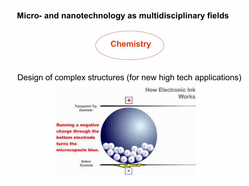
Design of complex structures (for new high tech applications)
Chemistry

Micro- and nanotechnology as multidisciplinary fields
Design of complex structures (for new high tech applications)
Chemistry
Photonic crystals and foams

Colloidal particles and their assemblyColloidosomes
Schematic illustration of the self-assembly process for colloidosomes.
(A) Aqueous solution is added to oil containing colloidal particles. Aqueous droplets are formed by gentle continuous shearing for several seconds.
(B) Particles adsorb onto the surface of the droplet to reduce the total surface energy. These particles are subsequently locked together by addition of polycations, by van der Waals forces, or by sintering the particles.
(C) The structure is transferred to water by centrifugation. The same approach is used to encapsulate oil droplets with a shell of particles from an exterior water phase. Particles adsorbed because of the large oil-water surface energy, which is substantially larger than the difference between the particle-oil and particle-water surface energies; this differs substantially from previous reports, where colloidal particles were adsorbed electrostatically onto oil droplets, which required prior treatment of the droplet’s surface
A. D. Dinsmore, et al. Science 298, 1006 (2002)

Colloidal particles and their assemblyColloidosomes
A. D. Dinsmore, et al. Science 298, 1006 (2002)

Micro- and nanotechnology as multidisciplinary fields
Nature as lecturer – Biomimetic approach
Chemistry

Micro- and nanostructures through self-assembly
Diatomes – self assembled complex structures

Micro- and nanotechnology as multidisciplinary fields
Nature as lecturer – The cell as microsystem with nanofunctional units
Molecular- / Cell- Biology

Micro- and nanotechnology as multidisciplinary fields
Nature as lecturer – Molecular motors in biology (translation & rotation)
Molecular- / Cell- Biology

Micro- and nanotechnology as multidisciplinary fields
Man-machine interfacingIntegrating biological function into microsystems
Engineering sciences
Neuron attached to a microchip(MPI Martinsried- Munich)

Micro- and nanotechnology as multidisciplinary fields
Creating new microproduction technology
Engineering sciences

Micro- and nanotechnology as multidisciplinary fields
Creating new microdevice technology
Engineering sciences
Microfluidics
Monolitic fabrication:
Integration of differentfunctional units Without assembly process

2‘ nd lecture 09.11.2009
Lithographical MethodsPhysical Principles
TechnologiesMaterials

Polymers in micro- and nanotechnology
3d structures2d structuresLateral structures
DNA Chip Microfluidic channel

3d structures2d structuresLateral structures
D
D: lateral resolution D: lateral resolutionH: height
Aspect ratio α
α = H/D
D
D

Top down technologies for micro-/nanostructure preparation
1 µm10 µm100 µm 100 nm 10 nm 1 nm
Sub-micrometer
Optical Lithography
Ebeam Lithography
Softlithography
AFM based Lithography

Top down technologies for micro-/nanostructure preparation
2d,3d Electronbeam & Optical, X-ray Lithography,
2d,3d Soft-Lithography
2d AFM based Lithography (dip pen, SNOM,..)

Ebeam and optical lithography
Substrate
Resist layer
Resist layerPositive resist
(becomes soluble upon irradiation)Negative resist
(becomes insoluble upon irradiation)
Pattern transfer
Irradiation

Film formation by spin coating
Substrate
Resist layer
Inhomogeneous thickness of resist layer and time evolution of layer thickness

Film formation by spin coating
Process and materials parameter influencing film thickness
• Solution viscosity • Solid content • Angular speed • Spin Time

Wetting of (polymer) solutions on solid substrates
ω ~ 0 deg. Spreading
0 < ω < 90 deg. Wetting
ω > 90 deg. Non-wetting

Wetting and dewetting of thin polymer (liquid films) on solidsubstrates

Stability of thin films on surfaces
1) Stable film , 2) Unstable film 3) Metastable filmΦ effective interface potential
R. Seemann, S. Herminghaus, and K. Jacobs, PRL 86 (2001) 5534

Stability of thin films on surfaces
R. Seemann, S. Herminghaus, and K. Jacobs, PRL 86 (2001) 5534

Stability of thin films on surfaces
R. Seemann, S. Herminghaus, and K. Jacobs, PRL 86 (2001) 5534
SiSiOPolymerfilm
dh
h: thickness of polymer filmd: Thickness of SiO layer

Stability of thin films on surfaces on variable SiO interface
R. Seemann, S. Herminghaus, and K. Jacobs, PRL 86 (2001) 5534

Wetting and partial wetting on surfaces
G. Reiter et. Al. Langmuir 15 (1999) 2551

25.10.2010

Optical lithography
Thick layer resist technology : High aspect ratios

Optical lithography
Thick layer resist technology : High aspect ratios
H
I(d)
I(d) = I * exp- ε * d
Inhomogeneous irradiation of polymer due to strong optical absorption (H > 100 µm)

Optical lithography
Thick layer resist technology : Thick layer resist systems (SU-8)

Optical lithography
T-BOC cleavage
Acid catalyst negative resist
Alkaline development
Chemically amplified negative resist

Optical lithography
T-BOC cleavage
Acid catalyst negative resist
Alkaline development
Chemically amplified negative resist

3‘ rd lecture 25.10.2010

Optical lithography
Light sources and structure resolution
Hg KrF ArF F2
365nm
248nm
193nm
157nm

Optical lithography
Lenses for KrF laser sources (248 nm)
Structure resolution <180 nm
Lense Material Calziumfluorid
Optical Transmission highabove 170 nm
No birefringence

Optical lithography
Lenses for ArF laser sources (198 nm)
Structure resolution 80 nm
Increasing na to ~ 1.3

Optical lithography
Resist for 157 nm VUV Lithography

Optical lithography
Resist for 157 nm VUV Lithography

Optical lithography
Two-photon lithography for complex 3d structures

Optical lithography
Two-photon lithography for complex 3d structures

Optical lithography
Two-photon lithography for complex 3d structures

Optical lithographyTwo-photon lithography for complex 3d structures

Optical lithographyQuantum dots as 2 photon initiators
CdS
o
o
o o
( )
2 hν
N.C. Strandwitz JACS 2008, 130(26), 8280-8288

Optical lithographyin aqueous solutions
Jhaveri, et. al. Chem. Mater. 2009, 21 (10), 2004 ff.

Optical lithography2 Photon photoabsorption

Optical lithography of complex 3d microstructures Multiphoton fabrication of chemically responsive protein hydrogels for microactuationBryan Kaehr and Jason B. Shear , PNAS 105 (2008) , 8850 ff.
Dynamic cell enclosures

Optical lithography of complex 3d microstructures Multiphoton fabrication of chemically responsive protein hydrogelsBryan Kaehr et. al. , PNAS 101 (2004) , 16104 ff.
Guiding neurons by crosslinked BSA

Optical lithographyin aqueous solutions
Jhaveri, et. al. Chem. Mater. 2009, 21 (10), 2004 ff.

Maskless optical lithography - A simple setup
Musgraves et. al. Am. J. Phys. 2005, 73 (10), 980 ff.
100 µm lines 500 µm pitch

Maskless optical lithography – 3d stereolithography
Sun et. al. Sensors and Actuators A 121, 2005, 113 ff.

Maskless optical lithography – 3d stereolithography
Choi et. al. J. Mat. Process. Tech. 209, 2009, 5494 ff.

Maskless optical lithography – 3d stereolithography
Choi et. al. J. Mat. Process. Tech. 209, 2009, 5494 ff.
Kidney scaffold

DMD chip element
Monk et. al. Microelectronic Eng., 27, 1995, 489 ff.

Optical lithography in microfluidic systems
Lee et. al. Lab Chip 9, 2009, 1670 ff.

Optical lithography in microfluidic systems
Chung et. al. Nature Materials 7, 2008, 581 ff.

Optical lithography in µ-fluidic systems – Particle assembly
Chung et. al. Nature Materials 7, 2008, 581 ff.

Multi-LED array
Grossmann et. al. J. Neural Eng., 11, 2010, 016004 ff.

Multi-LED array
Grossmann et. al. J. Neural Eng., 11, 2010, 016004 ff.
Local stimulation of nerve cells

Ebeam lithography Penetration depth of electrons with different energies in different materials

Ebeam lithography Penetration depth of electrons with different energies
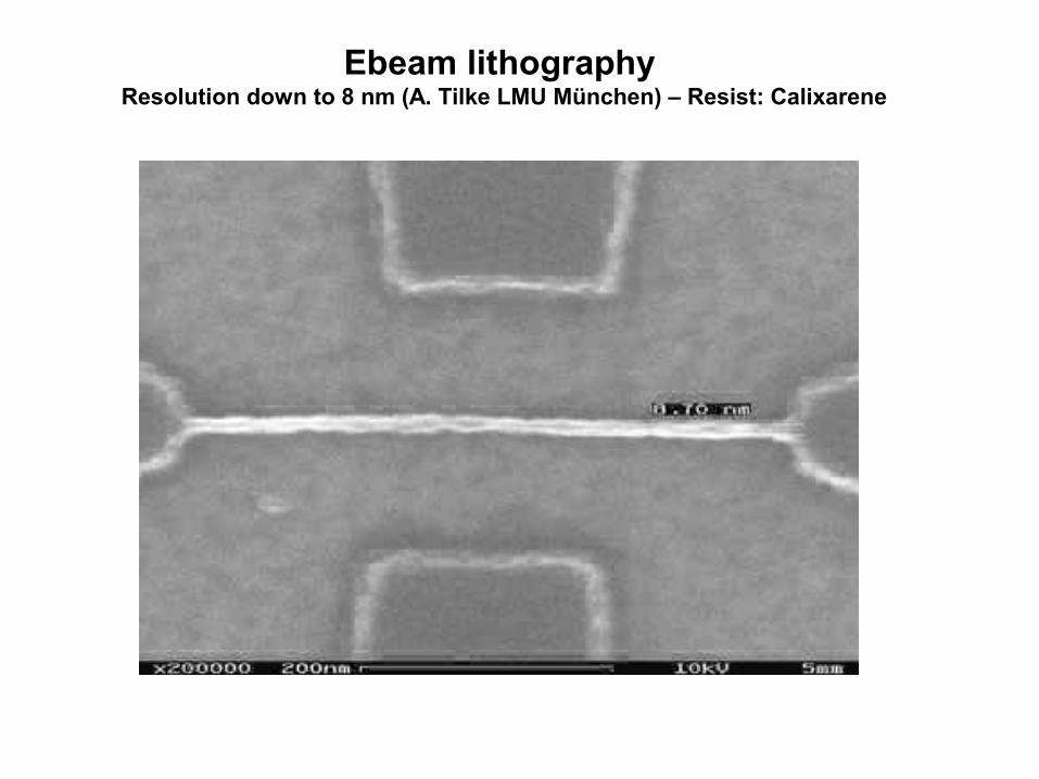
Ebeam lithography Resolution down to 8 nm (A. Tilke LMU München) – Resist: Calixarene

Ebeam lithography Chemical structure of Calixarene

Ebeam lithography SCALPEL Technique

Ebeam lithography SCALPEL Technique

Synchroton lithography / SynchrotonX-rays

Synchroton lithography X-rays

Synchroton lithography / LIGA X-rays

Synchroton lithography / Mask productionX-rays

Polymer embossing
Embossing machine(Jenoptik)
Process stepsCycle time ~ 7 minutes
Heating of substrate and tools above Tg
Application of pressure (~ kN)
Cooling of substrate and embossingtool below Tg
Removal of tool

Polymer embossing
Silicon master embossing tool Polymer replica made by embossing

Polymer microysystems
Lensarrays Beam splitter

Microdropdeposition


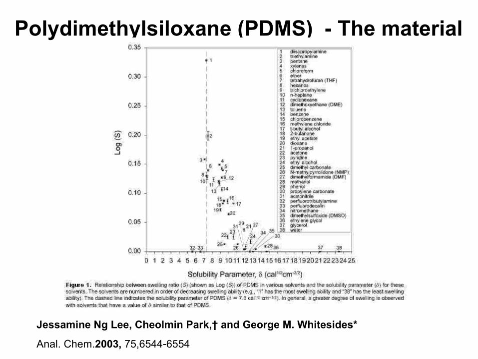
Polydimethylsiloxane (PDMS) - The material
Linear flexible polymer (liquid @RT)
Pt
Curing
CrosslinkingFlexible crosslinkedRubber ( @RT)
- Me : - CH3

Polydimethylsiloxane (PDMS) - The material
Chemical crosslinking by hydrosilylation
Schmid,H. Macromolecules 33, 3042 (2000)

Polydimethylsiloxane (PDMS) - The material
Chemical modification by hydrosilylation
(-O-CH2-CH2)- EO
Hydrophilic
Polydimethylsiloxane (PDMS) - The material
Jessamine Ng Lee, Cheolmin Park,† and George M. Whitesides*
Anal. Chem.2003, 75,6544-6554

Polydimethylsiloxane (PDMS) - The materialT.R.E. Simpsona, Z. Tabatabaianb, C. Jeynesb, B. Parbhooc, and J.L. Keddiea*

Polydimethylsiloxane (PDMS) - The materialHydrophilization by surface plasma treatment
O. Steinbock, Langmuir 19, 8117 (2003)

Liquid filling of a capillary by Surface interactions
S. Stark,Microelectronic Eng. 67/68, 229 (2003)

S. Stark,Microelectronic Eng. 67/68, 229 (2003)
Liquid filling of a capillary by Surface interactions

Polydimethylsiloxane (PDMS) - The materialHydrophilization by surface plasma treatment
O. Steinbock, Langmuir 19, 8117 (2003)

Polydimethylsiloxane (PDMS) - The materialHydrophilization by surface plasma treatment
M. Meincken, T.A. Berhane, P.E. Mallon, Polymer 46 (2005) 203–208
Hydrophobic recovery measured by surcface force AFM

Polydimethylsiloxane (PDMS) - The material
Compression mold 2 N/mm2
Compression mold 9.7 N/mm2
Schmid,H. Macromolecules 33, 3042 (2000)

Permeation induced flow in PDMS channels
P. Silberzan, Europhys. Letters 68, 412 (2004)

Permeation induced flow in PDMS channels
P. Silberzan, Europhys. Letters 68, 412 (2004)

Permeation induced flow in PDMS channels
P. Silberzan, Europhys. Letters 68, 412 (2004)

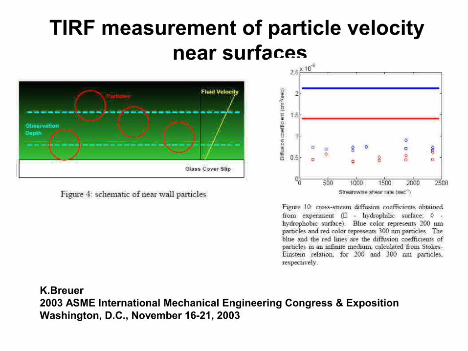
TIRF measurement of particle velocity near surfaces
K.Breuer2003 ASME International Mechanical Engineering Congress & ExpositionWashington, D.C., November 16-21, 2003
TIRF measurement of particle velocity near surfaces
K.Breuer2003 ASME International Mechanical Engineering Congress & ExpositionWashington, D.C., November 16-21, 2003

Unconventional lithographic techniques

Unconventional lithographic techniques

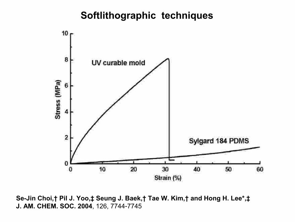
Softlithographic techniques
Se-Jin Choi,† Pil J. Yoo,‡ Seung J. Baek,† Tae W. Kim,† and Hong H. Lee*,‡J. AM. CHEM. SOC. 2004, 126, 7744-7745

Softlithographic techniques
Se-Jin Choi,† Pil J. Yoo,‡ Seung J. Baek,† Tae W. Kim,† and Hong H. Lee*,‡J. AM. CHEM. SOC. 2004, 126, 7744-7745
UV induced radical polymerisation of polyurethaneacrylates
Softlithographic techniques
Se-Jin Choi,† Pil J. Yoo,‡ Seung J. Baek,† Tae W. Kim,† and Hong H. Lee*,‡J. AM. CHEM. SOC. 2004, 126, 7744-7745

Softlithographic techniques
Se-Jin Choi,† Pil J. Yoo,‡ Seung J. Baek,† Tae W. Kim,† and Hong H. Lee*,‡J. AM. CHEM. SOC. 2004, 126, 7744-7745

Rigiflex lithography
Se-Jin Choi,† Pil J. Yoo,‡ Seung J. Baek,† Tae W. Kim,† and Hong H. Lee*,‡J. AM. CHEM. SOC. 2004, 126, 7744-7745

Rigiflex lithography
Se-Jin Choi,† Pil J. Yoo,‡ Seung J. Baek,† Tae W. Kim,† and Hong H. Lee*,‡J. AM. CHEM. SOC. 2004, 126, 7744-7745

Softlithographic techniques
Zentel , Advanced Materials 14, 588 (2002)

Softlithographic techniques Polymerisable conducting polymer
Zentel , Advanced Materials 14, 588 (2002)

PDMS based complex microfluidic systems
S. Quake,Science 298, 580 (2002)
Multilayer µ-fluidic systems
a) Fluidic transport layer
b) Control layer

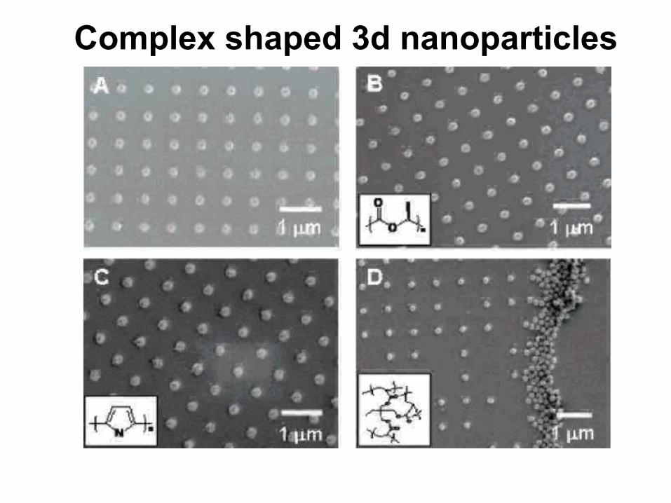
Complex shaped 3d nanoparticles
S.E.A. Gratton et al. / Journal of Controlled Release 121 (2007) 10–18
Larken E. Euliss, Julie A. DuPont, Stephanie Gratton and Joseph DeSimoneChem. Soc. Rev., 2006, 35, 1095–1104

Complex shaped 3d nanoparticles
Larken E. Euliss, Julie A. DuPont, Stephanie Gratton and Joseph DeSimoneChem. Soc. Rev., 2006, 35, 1095–1104
S.E.A. Gratton et al. / Journal of Controlled Release 121 (2007) 10–18
Complex shaped 3d nanoparticles

Complex shaped 3d nanoparticles
Jason P. Rolland,† Benjamin W. Maynor,† Larken E. Euliss,† Ansley E. Exner,†Ginger M. Denison,† and Joseph M. DeSimoneJ. AM. CHEM. SOC. 9 VOL. 127, NO. 28, 2005 10099

Complex shaped 3d nanoparticles
Larken E. Euliss, Julie A. DuPont, Stephanie Gratton and Joseph DeSimoneChem. Soc. Rev., 2006, 35, 1095–1104


Polymers in micro- and nanotechnology
3d structures2d structuresLateral structures
DNA Chip Microfluidic channel

„Surface Engineering“
Tailored Surface Chemistry
SiO2 X3Si-O-R
Al2O3 (OH)3-P-O-R
Au, Cu, Ag HS-R

„Surface Engineering“
Surface Polymerized Polypeptides

Poly-γ-benzylglutamate
Orientational Change of α-Helix by solventResulting change in layer thickness

Poly-γ-benzylglutamate
Orientational Change of α-Helix by solventResulting change in layer thickness


„Surface Engineering“
Surface Patterning
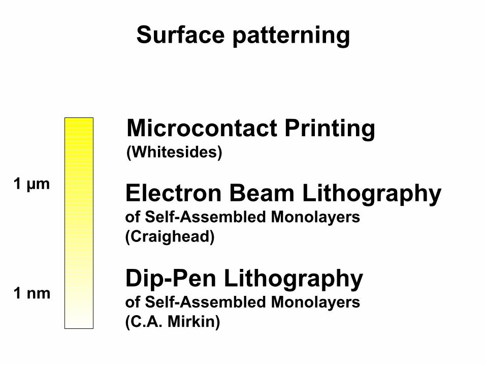
Surface patterning
Microcontact Printing(Whitesides)
Electron Beam Lithography of Self-Assembled Monolayers(Craighead)
Dip-Pen Lithography of Self-Assembled Monolayers(C.A. Mirkin)
1 µm
1 nm

Micro-contact printing
Siliconmicrostructure
or PMMA resist
Polymer stamp
(PDMS)

Micro-contact printing
Polymer stamp
(PDMS)
„Ink“

Micro-contact printing
Polymer stamp
(PDMS)
„Ink“
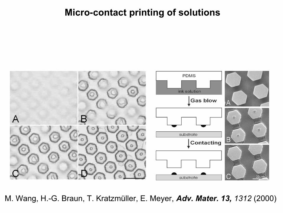
Micro-contact printing of solutions
M. Wang, H.-G. Braun, T. Kratzmüller, E. Meyer, Adv. Mater. 13, 1312 (2000)

Micro-contact printing of solutions
M. Wang, H.-G. Braun, T. Kratzmüller, E. Meyer, Adv. Mater. 13, 1312 (2000)

Micro-contact printing of dispersions
M.M. Sung,Lee B. Chem. Mater. 2007

Micro-contact printing of dispersions
M.M. Sung,Lee B. Chem. Mater. 2007
Colloidal particles on the mask

Micro-contact printing of dispersions
M.M. Sung,Lee B. Chem. Mater. 2007
Colloidal particles transfered to a surface by micro-contact printing(The particles are chemically attached to the surface)


![Cellulose Nanofibers and Other Biopolymers for Biomedical ... · pretreatments, such as enzymatic hydrolysis [14], partial carboxymethylation [15], ... protein animal-based polymers,](https://static.documents.pub/doc/80x56/5f4f8508db49655ce34d6e0e/cellulose-nanofibers-and-other-biopolymers-for-biomedical-pretreatments-such.jpg)


