Portable Telemedicine Monitoring Equipment 333 Second Prize Portable Telemedicine Monitoring Equipment Institution: HuaQiao University Participants: Huafeng Hong, Qianjiang, Yongjie Li Instructor: Ling Chaodong Design Introduction For our design, we wanted to provide a specialized in-home medical monitoring system. The following sections provide background information about health issues and telemedicine. Background Our project focuses on several issues, including: ■ Medical—In medicine today, the focus has shifted from disease treatment to prevention and health care. People care more about their health, and while disease prevention and health care have become an indispensable part of their lives, daily care for current physical conditions can eliminate problems and pain that could result from untreated conditions. ■ Social—With increasing attention on health and technological progress both home and abroad, home health care engineering (HHCE) is an emerging discipline. It advocates the concepts of medical treatment at home, self health care, and remote diagnosis, and combines technology with medical treatment. While addressing the trends of an aging society, soaring medical expenses, and increasing health demands in the 21st century, HHCE enables medical resource sharing and improves medical care in remote areas, making it well received by society. ■ Technological—Modern science and technology provides a technological basis for these designs. Embedded technology provides a leap forward and enables a diverse array of electronic products. Meanwhile, advancing network communications allows networked devices to share all kinds of
Transcript
Portable Telemedicine Monitoring Equipment
Second Prize
Portable Telemedicine Monitoring Equipment
Institution: HuaQiao University
Participants: Huafeng Hong, Qianjiang, Yongjie Li
Instructor: Ling Chaodong
Design IntroductionFor our design, we wanted to provide a specialized in-home medical monitoring system. The following sections provide background information about health issues and telemedicine.
BackgroundOur project focuses on several issues, including:
■ Medical—In medicine today, the focus has shifted from disease treatment to prevention and health care. People care more about their health, and while disease prevention and health care have become an indispensable part of their lives, daily care for current physical conditions can eliminate problems and pain that could result from untreated conditions.
■ Social—With increasing attention on health and technological progress both home and abroad, home health care engineering (HHCE) is an emerging discipline. It advocates the concepts of medical treatment at home, self health care, and remote diagnosis, and combines technology with medical treatment. While addressing the trends of an aging society, soaring medical expenses, and increasing health demands in the 21st century, HHCE enables medical resource sharing and improves medical care in remote areas, making it well received by society.
■ Technological—Modern science and technology provides a technological basis for these designs. Embedded technology provides a leap forward and enables a diverse array of electronic products. Meanwhile, advancing network communications allows networked devices to share all kinds of
333
Nios II Embedded Processor Design Contest—Outstanding Designs 2007
information easily. With improving manufacturing processes, chips are becoming more integrated and the resulting products are more portable and simplified.
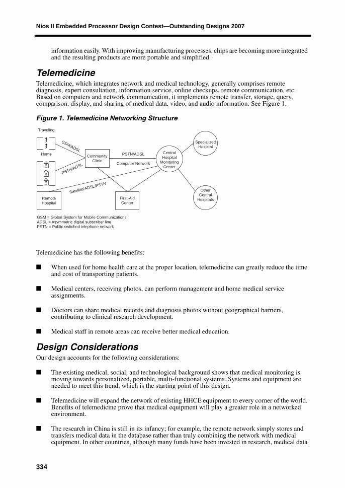
TelemedicineTelemedicine, which integrates network and medical technology, generally comprises remote diagnosis, expert consultation, information service, online checkups, remote communication, etc. Based on computers and network communication, it implements remote transfer, storage, query, comparison, display, and sharing of medical data, video, and audio information. See Figure 1.
Figure 1. Telemedicine Networking Structure
Telemedicine has the following benefits:
■ When used for home health care at the proper location, telemedicine can greatly reduce the time and cost of transporting patients.
■ Medical centers, receiving photos, can perform management and home medical service assignments.
■ Doctors can share medical records and diagnosis photos without geographical barriers, contributing to clinical research development.
■ Medical staff in remote areas can receive better medical education.
Design ConsiderationsOur design accounts for the following considerations:
■ The existing medical, social, and technological background shows that medical monitoring is moving towards personalized, portable, multi-functional systems. Systems and equipment are needed to meet this trend, which is the starting point of this design.
■ Telemedicine will expand the network of existing HHCE equipment to every corner of the world. Benefits of telemedicine prove that medical equipment will play a greater role in a networked environment.
■ The research in China is still in its infancy; for example, the remote network simply stores and transfers medical data in the database rather than truly combining the network with medical equipment. In other countries, although many funds have been invested in research, medical data
Traveling
RemoteHospital
CommunityClinic
PSTN/ADSL
Computer Network
First-AidCenter
CentralHospital
MonitoringCenter
SpecializedHospital
OtherCentral
Hospitals
GSM/ADSL
PSTN/ADSL
Home
Satellite/ADSL/PSTN
GSM = Global System for Mobile CommunicationsADSL = Asymmetric digital subscriber linePSTN = Public switched telephone network
334
Portable Telemedicine Monitoring Equipment
is still collected by expensive equipment, and data acquisition and network diagnosis are completed based on a PC and the Internet. Our design will provide a breakthrough in this respect.
■ Many design solutions exist today. Systems based on embedded processors such as monolithic, digital signal processors (DSPs), ARM processors, and the Nios® II processor are good solutions. We decided to use the Nios II soft-core processor for the following reasons:
● Altera’s flexible, efficient system-on-a-programmable-chip (SOPC) solution integrates the Nios II processor, memory, I/O interface, and other functional modules onto a single FPGA to form a programmable system-on-chip. It boasts a flexible design, many available intellectual property (IP) cores, as well as clipping, expansion, and upgrading.
● As an embedded soft-core processor, the Nios II processor features flexibility, high performance, low cost, and a long life cycle. Additionally, it comes with technical documentation and examples. Combined with an FPGA, you can develop anything that you can imagine, which is the key benefit of the Nios II processor and other soft-core CPUs. The Nios II processor supports μC/OS-II, μClinux, and many other real-time operating systems (RTOS), a light-weight TCP/IP (LwIP) stack, and zip file system, allowing users to add custom instructions and custom hardware accelerators, and to migrate customized peripherals and interface logic seamlessly. These features facilitate user designs while improving performance.
● Altera is at the forefront of FPGA embedded system development. As soft-core embedded technology evolves, we will have a competitive edge in this field by mastering it early.
Based on these considerations, we decided to focus our design on user terminals that provide convenient, appropriate, operable, and Internet-enabled home telemedicine monitoring equipment for the aging population, young people, and children whose lives rely on technology (e.g., those suffering from accidents, disabilities, and congenital diseases), chronic disease patients, terminal cancer or AIDS patients, and special people (e.g., newborn babies or pregnant women).
Function DescriptionThe design offers an effective, convenient medical monitoring solution for home, community, and home-care doctors. Designed mainly for user terminals, the monitoring equipment allows individuals to easily check and analyze their health conditions by themselves and obtain physical information (e.g., biomedical signals such as ECG, EEG, EMG, respiration, temperature, etc). The equipment displays these signals in graphics or waveforms so that individuals know intuitively whether their health indicators are normal. Additionally, the caretaker can make preliminary pathological diagnosis using the equipment’s analysis function. The system stores the physical information for subsequent data analysis and processing. With the development of telemedicine, the system can connect patients to medical service (e.g., a hospital, private practitioner, or monitoring center) and deliver the physical information in real time to a remote database or doctor through the network. This feature helps manage medical information databases and provides remote monitoring and diagnosis, allowing individuals to enjoy timely and effective diagnosis without leaving home. See Figure 2.
335
Nios II Embedded Processor Design Contest—Outstanding Designs 2007
Figure 2. Functional Diagram
The design in Figure 2 has the following functionality:
■ Multi-way acquisition of biomedical signals—Simulated biomedical signals are collected modularly, e.g., a medical sensor and signal filtering/amplification modulation circuit and separate regulating cards collect different parameters. Because the physical signals frequency bands are below 2 K, we use an analog-to-digital (A/D) conversion chip with a 40 K sampling rate A/D conversion, and reserve a data port for card access.
■ Real-time display of physical information (graphics and data)—The design uses serial input for data acquisition, saving I/O interface resources and eliminating the synchronization problems caused by parallel input. The collected data is transferred to SDRAM cache by direct memory access (DMA), reducing the CPU load. A display cache is created in SDRAM, while DMA technology transfers data to the liquid crystal display (LCD) for viewing. We designed the A/D acquisition and LCD interface control IP ourselves.
■ User-friendly operating interface and diversified processing and analysis functions—We used a 320 x 240 thin-film transistor (TFT) LCD; migrating μC/GUI makes the interface more friendly and attractive. We provide four functional areas: monitoring, analysis, storage, and detection, and
Monitoring Interface
Channel 1Channel 2Channel 3Channel 4
Monitoring Interface
Fast FourierTransform
(FFT)
WaveformAnalysis
WaveformMagnification/
Reduction
Send Interface
Window DisplayingRemote Diagnosis
Information
Connect to Network
Hub
Keyboard
NetworkInterface
A/D Conversion Plate
RTDGrabbing Card
ECGGrabbing Card
EEGGrabbing Card
EMGGrabbing Card
SD CardInterface
UserInterface
Storage Interface
Save as:Length:Channel:Device:
Save
RTOSMultitask
Multi-WayAcquisition
RemoteMonitoring
336
Portable Telemedicine Monitoring Equipment
multiple sub-functions simplify the operations. We compiled algorithms for detection, analysis, and processing to the signal characteristics, ensuring high accuracy.
■ Multiple functional interfaces (e.g. for network, compact flash (CF) or secure digital (SD) card) to facilitate data storage and transfer—We used an SD card as the storage device and implemented an SD mode. We used the FAT16 file system for data access. A PS/2 interface enables interaction with the monitoring equipment.
■ Scalable interface and software upgrades—For hardware, we provided a USB port, serial port, Integrated Development Environment (IDE) interface, and drivers for platform updates. The design adopts a RTOS to support application installation and upgrading.
■ Embedded web server allows the monitoring equipment to access and receive data via Ethernet—We used the DM9000A network interface chip that has chip control IP that allows us to access the network easily. In the protocol layer, Altera provides a LwIP software component that comprises all protocols required by the network. We used a socket application programming interface (API) to write web server programs that made network communication easy. The design allocates an IP block for the monitoring equipment or uses DHCP. DHCP allows a remote PC to access the monitoring equipment through the Internet to obtain real-time data and parameters and send diagnosis information to local monitoring equipment through the web page’s input area, implementing remote monitoring. Additionally, data can be saved to a remote database for management.
Performance ParametersThe following sections provide the design’s resource usage and performance parameters.
Resource UsageFigure 3 shows the design’s system resource utilization given by the Quartus® II software. The system has 109.90-MHz fMAX performance.
Figure 3. System Resource Utilization
The one-way A/D sampling controller uses 203 logic elements (LEs) and 8,192 memory bits (corresponding to a 512 bytes x 2 cache). It has a sampling frequency in the range of 0 to 1.667 MHz because the TLC549 sampling controller’s maximum frequency is 40 kHz and the system’s sampling frequency must be 0 to 40 kHz. If the sampling frequency set in software is 1,000 Hz, the output sampling frequency is 999.98 Hz. Figure 4 shows the A/D chip sampling rate.
337
Nios II Embedded Processor Design Contest—Outstanding Designs 2007
Figure 4. A/D Chip Sampling Rate
The system software uses 3,046 Kbytes for storage.
Design Performance ParametersThe following sections describe the performance parameters of the design.
Front-End Acquisition BoardTable 1 shows the pre-amplifier channel bandwidth test. The pre-amplifier gain is stable between frequency bands of 1 to 1 kHz, i.e., the channel bandwidth is ≥ 1 kHz.
Table 2 shows the amplifying power of the amplifier for different signals. At 20- and 50-Hz frequencies, the amplifier gains are stable when the input signal amplitude changes.
Table 3 shows the trapper’s trap feature test. The attenuation degree is increased by compromising trap impedance, i.e., a proper point is adjusted to obtain the attenuation and trap impedance.
Table 1. Pre-Amplifier Gain Changes with Frequency
SD Card Parameter TestThe test uses 100 16-bit data for reading/writing text files, which takes 40 ms. Assuming that the front-end data sampling is 2 kHz and 2,000 data points are collected every second, the storage time would be (2,000/100) x 40 ms = 800 ms. The test result shows that the collected data is not lost. See Table 4.
Network Speed TestWe set the monitoring equipment’s IP address to 192.168.220.236 in the test using the Linkwan.com web site test tool. Figure 5 shows the test result.
Figure 5. IP Address Test
We tested the operation of the built-in ping command as shown in Figure 6.
Figure 6. Ping Command Test
ECG Signal Detection ResultTable 5 shows the R-wave detection results and Table 6 shows the data compression result. The data source is the MIT/BIT ECG database, with 250-Hz sampling, 8-bit quantification, and four signal groups collected for detection. The ECG detection algorithm’s average R-wave false detection rate is
Table 4. SD Card File Operation Functions
Operation FunctionFile system start/exit FS_EXIT(), FS_INIT
Nios II Embedded Processor Design Contest—Outstanding Designs 2007
0.58%, the data compression ratio is as high as 13.75 times, and the correlation coefficient (CC) reaches 98.9%. The indicators are generally at a high level.
Design ArchitectureThe monitoring equipment mainly consists of three modules (see Figure 7):
■ Front-end collection and modulation
■ Signal processing, storage, and transfer platform
■ Remote monitoring
Figure 7. System Structure
Table 5. R-wave Detection Result
Signal Total Heart Rate
False Accept Rate
Undetected False Detected
Heart Rate
False Detection Rate (%)
Sddb-30 1,545 4 1 5 0.32
Sddb-32 2,013 6 7 13 0.66
Sddb-35 3,326 15 14 29 0.87
Sddb-37 2,111 4 6 10 0.47
Table 6. Data Compression Result
Signal CR Compression Ratio (%) PRD (%) Correlation Coefficient (%)Sddb-30 19 7.3 99.7
Sddb-32 11 16 98.8
Sddb-35 12 23 97.9
Sddb-37 13 13 99.2
ECG
EEG
EMG
RTD
GrabbingCard
A/D General-Purpose I/O (GPIO)
Nios II Processor& Operating System
Remote Monitoring
Ethernet NetworkControl
ChipSDRAM
DE2 Processing Platform
LCD
PS2P MouseTouch Screen
SD Card
340
Portable Telemedicine Monitoring Equipment
The hardware platform is the Development and Education (DE2) board, which contains the Altera® Cyclone® II EP2C35F672C6 FPGA. The hardware integrates the Nios II soft-core processor, memory, IP functions, and I/O ports on a single FPGA via SOPC technology. Peripheral hardware, including the data acquisition module, network, LCD screen, touch screen/keyboard, USB/SD memory, etc., are extended with a scalable I/O interface to facilitate system upgrades. Figure 8 shows the hardware platform.
Figure 8. SOPC Hardware Platform
Because our hardware platform is designed using SOPC concepts, the Nios II system is written using a hardware abstraction layer (HAL) driver, including the A/D conversion control IP core, LCD control core, network control IP, SD card control core, PS2 IP, etc. For multi-tasking, we used μC/OS-II for system dispatching. Additionally, we migrated μC/GUI and μC/FS as our graphical interface and file system, respectively. The LwIP protocol stack is a part of the software layer, and performs TCP/IP network communication. Other applications include a web server, operating interface, signal processing, fast Fourier transform (FFT) algorithm, and data compression. Figure 9 shows the software layer structure.
JTAGDebugging Module
Nios IIProcessor
SDRAM Controller
On-Chip ROM
Tri-State Bridge
DMA
GPIO
SDRAMMemory
SRAMMemory
SDRAMMemory
Software DebuggingReset Clock
FPGA
DSP Module
Timer
A/DInterface Module
LCDInterface Module
NetworkInterface Module
SDInterface Module
USBInterface Module
PowerManagement
Module
A/DEquipment
LCD Screen
LAN91C111
SD MemoryCard
USB Equipment
AVA
LON
Sw
itch
Bus
Completion of DataCollection, Display,
Processing, Storageand Transport
341
Nios II Embedded Processor Design Contest—Outstanding Designs 2007
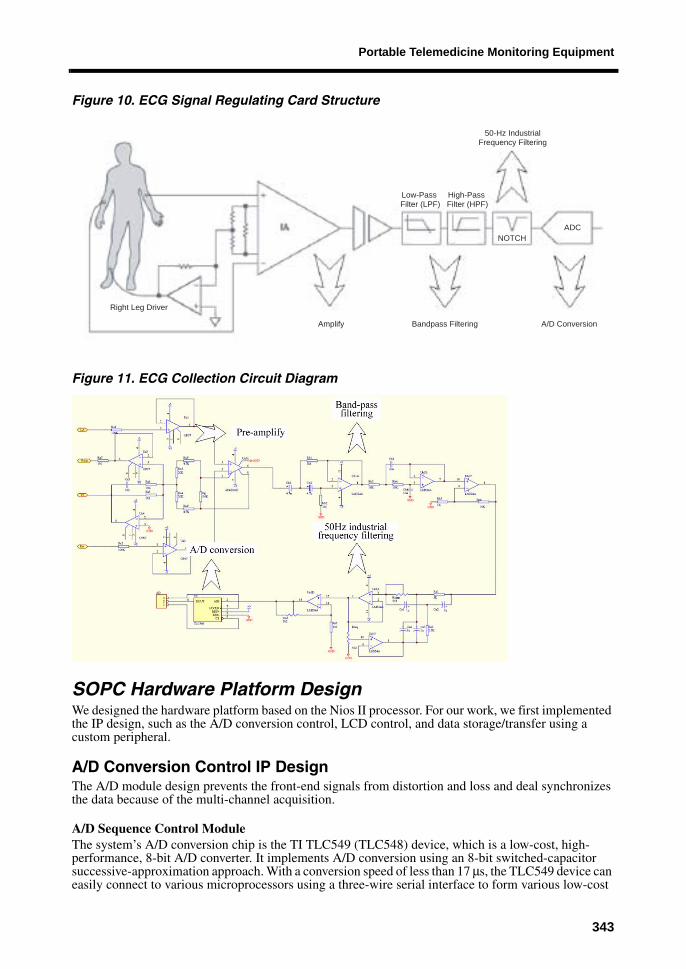
Biomedical Signal Regulation Card DesignThe biomedical signals are collected modularly, including the medical sensor, signal filtering amplifying modulation circuit, and A/D sampling circuit. The modulation circuit selects different filters and the amplified circuit according to the spectrum and scope of different biomedical signals. Using ECG as an example, the signal is amplified via the pre-amplification block, including a right leg driver to suppress common mode interference, a shield wire driver to eliminate lead wire interference, and the tenfold set gains.
We designed the pre-amplification block using the Analog Devices AD620 medical amplifier. The AD620 device is based on a modification of the classic three operational amplifier approach and is integrated using a co-phase differential amplifier in parallel. The AD620 device has a wide power supply range (± 2.3 V to ± 18 V), small size, and low power (it uses only a 1.3 mA maximum supply current), making it a good fit for low-voltage, low-power applications. Other advantages include a high common-mode rejection ratio, sound temperature stability, amplified bandwidth, and low noise. The amplified signal is further magnified using filtering and a 50-Hz trap filter. The post gain is set as 1 to 100. Because the maximum ECG signal is several mV and the A/D conversion input signal is over 1 V, the total gain is set as 1 to 1,000. Filtering uses a voltage-controlled voltage source second-order high (low) pass filter to eliminate signals interference such as myoelectricity beyond 0.05 to 100 Hz, as well as other high-order industrial frequency harmonics. Additionally, we used an active twin-T band-stop filtering circuit to curb the 50-Hz industrial frequency interference.
The A/D sampling chip is the Texas Instruments (TI) 8-bit serial TLC549 device. It uses a serial peripheral interface (SPI) to provide collection control and data transmission using three wires. It provides an on-chip system clock that typically operates at 4 MHz, as well as a software/hardware controlled circuit with a conversion time of less than 17 μs and a sampling rate of 40 kilosamples per second (KSPS). With a differential voltage reference, the TLC549 device can measure a minimum value of 1,000 mv/256, i.e., 8-bit resolution can be obtained without amplifying the 0- to 1-V signal. Figure 10 shows the ECG signal regulating card structure and Figure 11 shows the circuit diagram.
LCD Operating InterfaceApplication
Data Compression/Signal ProcessingData Analysis/Data Access
Web ServerApplication
LCD Driver AD ConversionControl Driver
SD Card Driver Network Driver Input DeviceDriver
LwIP NetworkProtocol Stack
μC/GUI μC/FS
μC/OS-II RT0S
HAL API
342
Portable Telemedicine Monitoring Equipment
Figure 10. ECG Signal Regulating Card Structure
Figure 11. ECG Collection Circuit Diagram
SOPC Hardware Platform DesignWe designed the hardware platform based on the Nios II processor. For our work, we first implemented the IP design, such as the A/D conversion control, LCD control, and data storage/transfer using a custom peripheral.
A/D Conversion Control IP DesignThe A/D module design prevents the front-end signals from distortion and loss and deal synchronizes the data because of the multi-channel acquisition.
A/D Sequence Control ModuleThe system’s A/D conversion chip is the TI TLC549 (TLC548) device, which is a low-cost, high-performance, 8-bit A/D converter. It implements A/D conversion using an 8-bit switched-capacitor successive-approximation approach. With a conversion speed of less than 17 μs, the TLC549 device can easily connect to various microprocessors using a three-wire serial interface to form various low-cost
Right Leg Driver
Amplify Bandpass Filtering A/D Conversion
Low-Pass Filter (LPF)
NOTCHADC
50-Hz IndustrialFrequency Filtering
High-Pass Filter (HPF)
343
Nios II Embedded Processor Design Contest—Outstanding Designs 2007
test and control application systems. With a differential voltage reference, the TLC549 device can measure the minimum value of 1,000 mv/256, i.e., we can obtain 8-bit resolution without amplifying the 0- to 1-V signal. Sequence control is generated according to the sequence diagram shown in Figure 12.
Figure 12. TLC549 Sequence Diagram
According to the sequence, the following tasks are performed when eight external clock signals are input at the TLC549 device’s I/O clock: read the previous A/D conversion result, sample and reserve the input analog signal converted currently, and initiate A/D conversion.
To implement the TLC549 analog controller in the FPGA, we designed the simulation with a Verilog HDL control state machine as shown in Figure 13:
Figure 13. State Machine Sequence
din is the serial input of data collected, and the clock is obtained through frequency division coefficient. fsm is the sampling control clock to adjust sampling speed as required.
Double-Buffered Operating TechnologyBecause A/D sampling is short, it is impractical to query or read data with interrupts. Therefore, the buffer design must reduce the interruption time by temporarily storing the converted data for N times in the buffer memory. To collect data continuously and correctly implement a seamless buffer, we use a ping-pong operation structure with double-buffer storage that takes advantage of the FPGA’s design flexibility. The ping-pong operation is a handling technique for the data stream (see Figure 14). The data buffer module can be any storage unit and in this design we use dual-port RAM (DPRAM).
344
Portable Telemedicine Monitoring Equipment
Figure 14. Ping-Pong Operation
During ping-pong operation, the input data streams are distributed to two data buffer areas through the input data selection unit. The data buffer module can be any storage module, and the common storage units include DPRAM, single-port RAM (SPRAM), FIFO, etc. In the first buffer period, the input data stream is cached into data buffer module 1. In the second buffer period, the input data stream is cached into data buffer module 2 using the input data selection unit switch while the first period data in data buffer module 1 is output through the output port and the output data selection unit. In the third buffer period, the input data stream is cached into data buffer module 1 with the input data selection unit while the second period data in data buffer module 2 is switched by the output data selection unit and output via the output port for operation. The process repeats as required.
The ping-pong operation’s unique feature is the collaborative switching of the input and output data selection units according to a meter, which sends the buffered data streams to the data stream processing unit for operation without pausing. The ping-pong operation module is an independent function and the input and output data streams are continuous at the sides of the module; therefore, the design can process data streams in the form of a pipeline. Ping-pong operation is usually applied in a pipeline algorithm for seamless data buffering and processing.
This design implements a data cache by alternatively storing an A/D sampling sequence controller into two 512-byte DPRAM blocks. When DPRAM1 is full, the data is stored in DPRAM2 with one interrupt so that the system has enough time to move the data out of DPRAM1 when the controller writes data into DPRAM2. Figure 15 shows the DPRAM buffer system timing diagram.
Figure 15. DPRAM Buffer System Timing Diagram
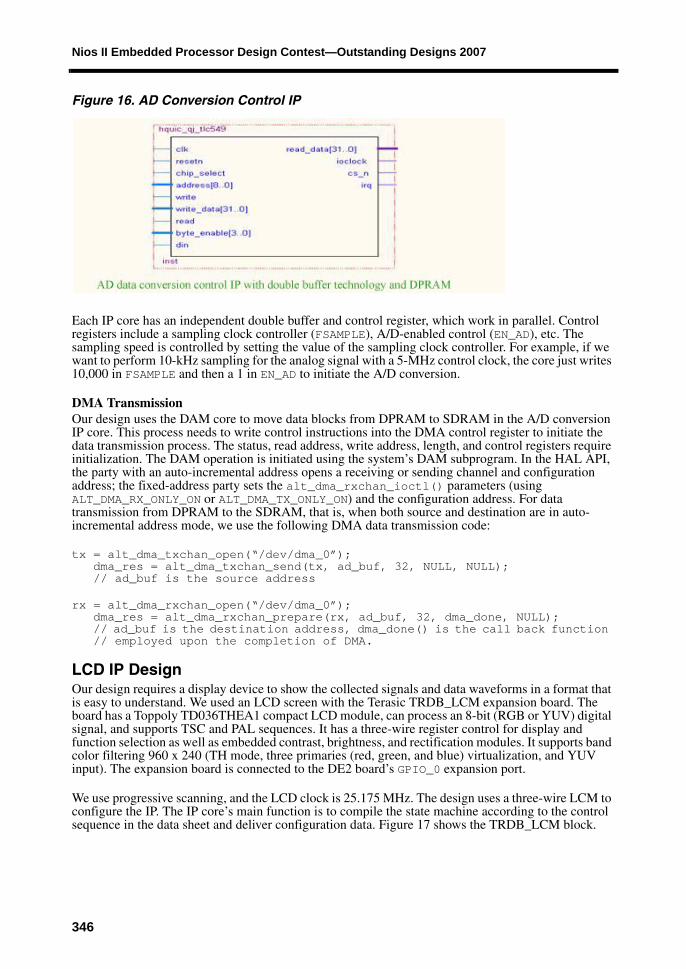
IP DesignThe final IP core in the A/D sampling module includes an A/D conversion sequence controller, a double-buffer ping-pong operation module, a control register such as a sampling clock frequency division controller, and a bus control signal. Figure 16 shows the A/D conversion control IP core structure, which can connect directly to the Avalon® bus and can be added to the system if necessary. Four cores are added to the system.
InputData
SelectionUnit
Data BufferModule 1
Data BufferModule 1
OutputData
SelectionUnit
345
Nios II Embedded Processor Design Contest—Outstanding Designs 2007
Figure 16. AD Conversion Control IP
Each IP core has an independent double buffer and control register, which work in parallel. Control registers include a sampling clock controller (FSAMPLE), A/D-enabled control (EN_AD), etc. The sampling speed is controlled by setting the value of the sampling clock controller. For example, if we want to perform 10-kHz sampling for the analog signal with a 5-MHz control clock, the core just writes 10,000 in FSAMPLE and then a 1 in EN_AD to initiate the A/D conversion.
DMA TransmissionOur design uses the DAM core to move data blocks from DPRAM to SDRAM in the A/D conversion IP core. This process needs to write control instructions into the DMA control register to initiate the data transmission process. The status, read address, write address, length, and control registers require initialization. The DAM operation is initiated using the system’s DAM subprogram. In the HAL API, the party with an auto-incremental address opens a receiving or sending channel and configuration address; the fixed-address party sets the alt_dma_rxchan_ioctl() parameters (using ALT_DMA_RX_ONLY_ON or ALT_DMA_TX_ONLY_ON) and the configuration address. For data transmission from DPRAM to the SDRAM, that is, when both source and destination are in auto-incremental address mode, we use the following DMA data transmission code:
tx = alt_dma_txchan_open(“/dev/dma_0”);dma_res = alt_dma_txchan_send(tx, ad_buf, 32, NULL, NULL); // ad_buf is the source address
rx = alt_dma_rxchan_open(“/dev/dma_0”);dma_res = alt_dma_rxchan_prepare(rx, ad_buf, 32, dma_done, NULL); // ad_buf is the destination address, dma_done() is the call back function // employed upon the completion of DMA.
LCD IP Design Our design requires a display device to show the collected signals and data waveforms in a format that is easy to understand. We used an LCD screen with the Terasic TRDB_LCM expansion board. The board has a Toppoly TD036THEA1 compact LCD module, can process an 8-bit (RGB or YUV) digital signal, and supports TSC and PAL sequences. It has a three-wire register control for display and function selection as well as embedded contrast, brightness, and rectification modules. It supports band color filtering 960 x 240 (TH mode, three primaries (red, green, and blue) virtualization, and YUV input). The expansion board is connected to the DE2 board’s GPIO_0 expansion port.
We use progressive scanning, and the LCD clock is 25.175 MHz. The design uses a three-wire LCM to configure the IP. The IP core’s main function is to compile the state machine according to the control sequence in the data sheet and deliver configuration data. Figure 17 shows the TRDB_LCM block.
346
Portable Telemedicine Monitoring Equipment
Figure 17. I2S_LCM Block
The LCD module does not have a display controller, so we designed it independently with Verilog HDL. The controller supports multiple color modes, including 18, 16, and 8 bpp, and self-defined mode. The image memory uses an on-chip FIFO buffer, which is adjustable according to design needs. A 256-color look-up table also adopts on-chip RAM. The image information can be read automatically from memory with DAM using the Avalon bus’s main module transmission port. Figures 18 and 19 show the system.
Figure 18. LCD IP Core Structure
Main DeviceSignal
Interrupt
Communicationwith Memory
AvalonMaster Port
Control Register
State Register
DMA Address Register
Interrupt Register
Color Pallet
Color ProcessingModule
DMA StateMachine
SequenceControlModule
LCDClock
HorizontalSynchronization
VerticalSynchronization
Valid DataAvalonSlavePort
RGBOn-Chip
FIFO
R (5:0)
B (5:0)
G (5:0)
347
Nios II Embedded Processor Design Contest—Outstanding Designs 2007
Figure 19. LCD IP Core RTL
The LCD core has four modules: the interface module, memory module, color conversion module, and sequence module.
The interface module operates the controller and reads the state. It contains a control register, state register, DMA address register, and interrupt register. See Table 7.
The control register’s EDMA initiates the DMA, PMODE selects the color pallet mode (18, 16, and 8 bpp, and self-defined), and EIRQ enables interrupts. The state register queries the interrupt state. The DMA address register sets and queries the DMA start address. The interrupt register clears interrupts.
The memory module reads the SDRAM’s FRAMEBUFFER data independently into an on-chip FIFO in DMA mode using a state machine that reads/writes the Avalon master port. Based on the sequence, the state machine has three states: idle, address, and data. In idle state, it waits for the DMA start-up signal and initializes the module transmission and DMA start address number. When the DMA enable signal is initiated and the on-chip FIFO buffer is idle, it jumps to the address state. In address state, the wait signal on the wait bus is cancelled to enter a data read state. In data read state, the read signal begins to
2 DMA address register Read & write Write the start address of DMA transmission
3 Interrupt register Read Clear interrupt
348
Portable Telemedicine Monitoring Equipment
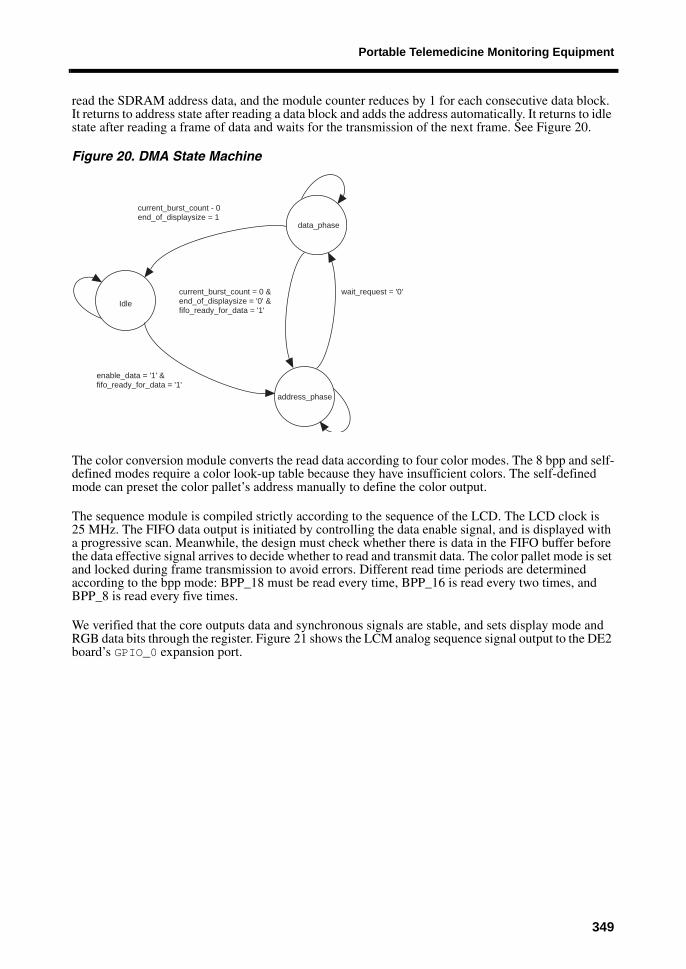
read the SDRAM address data, and the module counter reduces by 1 for each consecutive data block. It returns to address state after reading a data block and adds the address automatically. It returns to idle state after reading a frame of data and waits for the transmission of the next frame. See Figure 20.
Figure 20. DMA State Machine
The color conversion module converts the read data according to four color modes. The 8 bpp and self-defined modes require a color look-up table because they have insufficient colors. The self-defined mode can preset the color pallet’s address manually to define the color output.
The sequence module is compiled strictly according to the sequence of the LCD. The LCD clock is 25 MHz. The FIFO data output is initiated by controlling the data enable signal, and is displayed with a progressive scan. Meanwhile, the design must check whether there is data in the FIFO buffer before the data effective signal arrives to decide whether to read and transmit data. The color pallet mode is set and locked during frame transmission to avoid errors. Different read time periods are determined according to the bpp mode: BPP_18 must be read every time, BPP_16 is read every two times, and BPP_8 is read every five times.
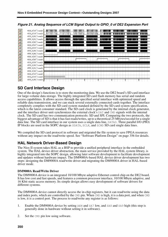
We verified that the core outputs data and synchronous signals are stable, and sets display mode and RGB data bits through the register. Figure 21 shows the LCM analog sequence signal output to the DE2 board’s GPIO_0 expansion port.
Nios II Embedded Processor Design Contest—Outstanding Designs 2007
Figure 21. Analog Sequence of LCM Signal Output to GPIO_0 of DE2 Expansion Port
SD Card Interface DesignOne of the design’s functions is to store the monitoring data. We use the DE2 board’s SD card interface for large-volume data storage. The highly integrated SD card flash memory has serial and random access capabilities. It allows access through the specified serial interface with optimized speed and reliable data transmission, and we can stack several externally connected cards together. The interface completely complies with the SD card system standard defined by the SD card system specification, which is the latest consumer standard. The SD card clock is generated by the internal clock generator, and the interface driver unit synchronizes the external clock’s DAT and CMD signals with the internal clock. The SD card has two communication protocols: SD and SPI. Comparing the two protocols, the biggest advantage of SD is that it has fast reads/writes, up to a theoretical 25 Mbytes/second for a single data line. The SD card interface in our system uses a single data line, DATA0. Three parallel I/O (PIO) IP blocks are used in the SOPC design as SDATA, SCLK, and SCMD SD card single data lines.
We compiled the SD card protocol in software and migrated the file system to save FPGA resources without any impact on the read/write speed. See “Software Platform Design” on page 356 for details.
HAL Network Driver-Based DesignThe Nios II system takes HAL as a BSP to provide a unified peripheral interface in the embedded system. The HAL device driver abstraction, the main service provided by the HAL system library, is highly integrated into the SOPC design, allowing later software development to facilitate development and updates without hardware impact. The DM9000A-based HAL device driver development has two steps: designing the DM9000A read/write driver and migrating the DM9000A driver in HAL-based driver mode.
DM9000A Read/Write DriverThe DM9000A device is an integrated 10/100 Mbyte adaptive Ethernet control chip on the DE2 board. It has low cost and fast speeds, and features a common processor interface, 10/100 Mbyte adaptive, and 16 Kbit static access memory. Its simple design allows easy development of software drivers for different systems.
The DM9000A device cannot directly access the in-chip registers, but it can read/write using the data and index ports, which are controlled by the CMD pin. When CMD is high, it is a data port, and when CMD is low, it is a control port. The process to read/write any register is as follows:
1. Enable the DM9000A device by setting AEN and SA7 low, and SA8 and SA9 high (this step is generally done in hardware without setting it in software).
2. Set the CMD pin low using software.
350
Portable Telemedicine Monitoring Equipment
3. Input the register location to be read/written on the index port.
4. Set CMD pin high.
5. Input/output the register data to be read/written at the material port. See Figures 22 and 23.
Figure 22. DM9000 Read Process
Figure 23. DM9000 Write Process
Develop DM9000A HAL Network Device DriverBecause the DM9000A device provides a complete bus interface, we need the Avalon bus and DM9000A interface logic in SOPC Builder. The DM9000A device communicate with the Nios II processor as an Avalon slave. Creating a HAL device driver includes creating device instances and registering the character device.
By referring to the HAL device driver development documentation and focusing on the lightweight IP (LwIP) driver structure, we defined the following structure DM9000A alt_dev structure:
#define ALTERA_AVALON_DM9K_INIT(dev)alt_lwip_dev_reg(dev) //initialize //devices, register in HAL.
SOPC BuilderThe Quartus II software’s SOPC Builder integrates a hardware system in an FPGA, including writing the CPU, memory, interface IP blocks, timer, and Avalon bus in a hardware description language, and presenting it in the form of an IP block. Using the DE2 development board and considering the design functionality, we created the SOPC system.See Figures 24 and 25.
352
Portable Telemedicine Monitoring Equipment
Figure 24. Nios II CPU Customization
Figure 25. 4-Mbyte Flash and 8-Mbyte SDRAM Controller Customization
The custom peripheral includes the A/D conversion control IP block, LCD control IP block, DM9000A bridge IP block, PS2 protocol resolution IP block, etc. See Figure 26.
Flash Control IP Customized Interface SDRAM Control IP Customized Interface
353
Nios II Embedded Processor Design Contest—Outstanding Designs 2007
Figure 26. Custom Peripheral Interface
Figure 27 shows the system in SOPC Builder. The system clock is 100 MHz and peripheral clock is 50 MHz. The clock is derived from an external phase-locked loop (PLL) that generates a double frequency clock. Designing our embedded system with SOPC Builder minimized our development time.
Figure 27. SOPC Builder Interface
Figure 28 shows the SOPC Builder-generated schematic diagrams in the Quartus II software.
354
Portable Telemedicine Monitoring Equipment
Figure 28. SOPC Builder-Generated Modules
355
Nios II Embedded Processor Design Contest—Outstanding Designs 2007
We added a PLL in the Quartus II software to distribute pins, and we generated the hardware SRAM Object File (.sof) after compilation. This step completed our project’s hardware platform, and we next entered the software phase.
Software Platform DesignThis section describes the software development for our design.
μc/OS-II Multi-Tasking DesignBecause our system involves many tasks, such as collection, display, networking, storage, etc., we used the real-time μC/OS-II operating system to manage the entire system, resulting in smooth operation of the hardware modules and application program. μC/OS-II has already been migrated to the Nios II Integrated Development Environment (IDE), so we only needed to select it in the IDE. We divided the main tasks as:
■ Display
■ Collection
■ Data storage
■ Network tasks
■ Signal processing
■ Input device
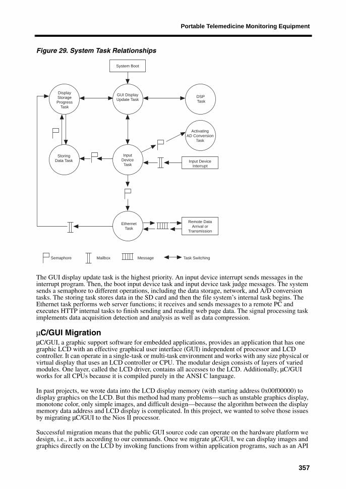
Display is the highest priority task. All main tasks have other relative subtasks. Figure 29 shows the relationship of the main tasks.
356
Portable Telemedicine Monitoring Equipment
Figure 29. System Task Relationships
The GUI display update task is the highest priority. An input device interrupt sends messages in the interrupt program. Then, the boot input device task and input device task judge messages. The system sends a semaphore to different operations, including the data storage, network, and A/D conversion tasks. The storing task stores data in the SD card and then the file system’s internal task begins. The Ethernet task performs web server functions; it receives and sends messages to a remote PC and executes HTTP internal tasks to finish sending and reading web page data. The signal processing task implements data acquisition detection and analysis as well as data compression.
μC/GUI MigrationμC/GUI, a graphic support software for embedded applications, provides an application that has one graphic LCD with an effective graphical user interface (GUI) independent of processor and LCD controller. It can operate in a single-task or multi-task environment and works with any size physical or virtual display that uses an LCD controller or CPU. The modular design consists of layers of varied modules. One layer, called the LCD driver, contains all accesses to the LCD. Additionally, μC/GUI works for all CPUs because it is compiled purely in the ANSI C language.
In past projects, we wrote data into the LCD display memory (with starting address 0x00f00000) to display graphics on the LCD. But this method had many problems—such as unstable graphics display, monotone color, only simple images, and difficult design—because the algorithm between the display memory data address and LCD display is complicated. In this project, we wanted to solve those issues by migrating μC/GUI to the Nios II processor.
Successful migration means that the public GUI source code can operate on the hardware platform we design, i.e., it acts according to our commands. Once we migrate μC/GUI, we can display images and graphics directly on the LCD by invoking functions from within application programs, such as an API
System Boot
DisplayStorageProgress
Task
StoringData Task
GUI DisplayUpdate Task
InputDeviceTask
EthernetTask
DSP Task
ActivatingAD Conversion
Task
Input DeviceInterrupt
Remote DataArrival or
Transmission
Semaphore Mailbox Message Task Switching
357
Nios II Embedded Processor Design Contest—Outstanding Designs 2007
drawing function. We can create fascinating, innovative images and graphics, implement a multi-tasking LCD, e.g., multiple windows, controls, anti-aliasing, etc., and be free from basic tasks such as the graphic data location in the LCD display memory. Undoubtedly, this method will greatly facilitate our future LCD development.
Figure 30 shows the μC/GUI software system.
Figure 30. μC/GUI Software System
Modifying the GUIconf.h and LCDconf.h files is an important migration step (see Figure 31). Some of the files we modify are described below.
■ GUICONF.h—In this file, we configure the GUI migration options for different operating systems. In our design, we configure migration to μC/OS-II and allow multi-tasking to invoke μC/GUI functions.
■ LCDconf.h—In this file, we define various attributes related to hardware, such as the LCD size, color, and interface function. The LCD driver interprets μC/GUI functions into the LCD interface function defined in the LCDConf.h file, which is not applicable to the hardware connection. Using the driver, the μC/GUI and LCD hardware interface converts the hardware interface function into an LCD read/write function as defined in the LCDConf.h file.
■ LCDDDummy.c (LCD drivers)—These two functions, LCD-L0-SetPixelIndex(int x, int y, int PixelIndex) and LCD-L0-GetPixelIndex(int x, int y), constitute the basic low-level LCD drive function and connect directly with the hardware. Some basic functions such as LCD-L0-DrawHLine, LCD-L0-DrawVLine and LCD-L0-FillRect are also defined in driver. They are invoked from LCD-L0-SetPixelIndex(int x, int y, int PixelIndex) and LCD-L0-GetPixelIndex(int x, int y).
----Four #defines above are operation over four registers of LCD. Initialize LCD controller #define LCD_INIT_CONTROLLER() LCD_WRITE_REG2(0X01F40000);\
LCD_WRITE_REG0(000001);#endif
SD Card-Based File System Migration Figure 32 shows the μC/FS structure, which, like μC/GUI, is public source code. Figure 33 shows the card-based layers.
Figure 32. μC/FS Structure
API Layer
File System Layer
Logical Block Layer
Device Driver
<stdio.h> like functions, such asFS_fopen, FS_fread, etc.
Translation of File Operations toSector Operations
Synchronization od Device Operationsfor Different File Operations
Low Level Routines to Access Sectorsof a Device and to Check Status
359
Nios II Embedded Processor Design Contest—Outstanding Designs 2007
Figure 33. SD Card-Based FS Layer
Some key points when migrating the file system (FS) are:
■ Because of μC/OS-II, we reduced unnecessary operating system (OS) source code in the FS to conserve storage space.
■ We modified the fs-port.h file to implement a data type that the Nios II processor can recognize. For the fs-conf.h file, we modified the relevant FS configuration, such as the number of opened files, names of supported devices, etc.
■ We determined the lowest level FS device driving function and added the SD card device-driven function.
In the SD card protocol, the host sends CMD first and then the card sends RES. If there is data to be transferred, it is transferred on the DATA line. Except for copyright protection commands, the SD protocol has 34 total commands. For users, configuring SD card means that the system reads/writes the register. The main registers include CID, CSD, and OCR. We used the C language to compile an SD driver in the Nios II IDE, i.e., one that performs initialization and data read/write functions.
In μC/FS, a low-level device driver invokes functions directly as shown in the following code and our SD card driver is implemented in the four functions listed.
We defined the card initialization process as SD-card-init() in μC/FS; GENDEV-DevStatus( ) invokes the process to perform the following functions:
1. Reset the card and its control module, and keep card frequency at no more than 25 MHz during the reset process. The card can be reset using the CMD method (CMD0.CMD52).
2. Determine whether the input card is an SD card or MMC using CMD55.
Application
Embedded File System
SD Memory Card Driver
SD Memory Card
File System Layer
Device Driver Layer
Hardware
360
Portable Telemedicine Monitoring Equipment
3. Obtain the card ID (CID) by transmitting CMD2. The CID is integrated in the card and each card has only one CID. Once CID is obtained, the card can enter certification status.
4. The relative card address (RCA) is the unique symbol that controller uses to access the card. Dynamic distribution is available using CMD3.
5. Set the read/write block size. According to the FAT and FS settings, we can set a read/write block as 512 bytes.
We enable the card reading/writing using the data block and every read/write is an integral multiple of the block. CMD17/CMD18 and CMD24/CMD25 read/write one or many data blocks over the card, respectively. In μC/FS, we implemented reading/writing in SD-read-Iba(Unit, Sector, pBuffer) and SD-write-Iba(Unit, Sector, pBuffer).
Data always has an attached cyclical redundancy check (CRC) code. In μC/FS, CRC codes are implemented with the GetCRC16() function.
Operating Interface DesignAll main monitor operations are merged onto the LCD; therefore, a user-friendly operating interface is key to the design. When we migrate the GUI, developing GUI-based operating interfaces will become faster and more efficient. Figure 34 shows the operating interface process.
361
Nios II Embedded Processor Design Contest—Outstanding Designs 2007
Figure 34. Operating Interface Process
Web Server DesignThe network communications design is based on the TCP/IP protocol. The key to successful communication is to embed the protocol into the system and migrate the network interface control chip driver to implement communication at the physical layer. At the application layer, we can implement communication by writing different applications according to the required services.
The LwIP protocol stack, is already integrated into the Nios II processor, accelerating the network development. Therefore, we only needed to focus on designing the network interface driver and developing the application.
StartInterface
MainInterface
MonitoringInterface
AnalysisInterface
StorageInterface
TransmissionInterface
ChooseMonitoringChannel
Choose AbnormalData Segment for
Analysis
Input Name and Sizeof Storage File and
Name of Device
Activate ConnectionNetwork and Choose
Channel for Sending Data
Beginto Store
Send Datato Long
Distance andWait for Remote
Message
Display of C
hannel 1 Startup
Display of A
bnormality 1 S
tartup
AnalyzeSpectrum?
SpectrumDisplay
WaveformZooming
Yes No
Display of A
bnormality 3 S
tartup
Display of A
bnormality 2 S
tartup
Display of A
bnormality 4 S
tartup
Display of C
hannel 1 Startup
Display of C
hannel 1 Startup
Display of C
hannel 1 Startup
362
Portable Telemedicine Monitoring Equipment
LwIP OverviewLwIP was originally written for embedded system by Adam Dunkels of the Swedish Institute of Computer Science. It can be migrated to an OS or operated independently. LwIP has the following features:
■ Supports IP forwarding with multiple network interfaces.
■ Supports the Internet control message protocol (ICMP).
■ Includes an experimental user datagram protocol (UDP).
■ Includes congestion control, round-trip time (RTT) estimation, TCP of fast recovery, and fast retransmission.
■ Provides a dedicated raw API for improving application performance.
■ Includes an optional Berkeley interface, an API (in case of multi-threading).
■ Supports the point-to-point protocol (PPP) in the latest version.
■ Has increased IP fragment support in the latest version.
■ Supports the DHCP protocol and dynamic IP address allocation.
To adapt to different operating systems, LwIP adds an OS-encapsulated layer between LwIP and the OS instead of using system calls and data structures relating to a certain OS. The layer provides a unified interface for OS service (timing, process synchronization, and messaging), uses semaphone for process synchronization, and mbox for messaging. The following code shows the OS encapsulated layer’s main functions:
)//create a new processsys_mbox_t sys_mbox_new(void)//create a new mailboxvoid sys_mbox_free(sys_mbox_t mbox)//release and delete a mailboxvoid sys_mbox_post(sys_mbox_t mbox, void *data) //send a message to the mailboxvoid sys_mbox_fetch(sys_mbox_t mbox, void **msg)//wait for a message in the mailboxsys_sem_t sys_sem_new(u8_t count)//create a new semaphorevoid sys_sem_free(sys_sem_t sem)//release and delete a semaphorevoid sys_sem_signal(sys_sem_t sem)//send a semaphorevoid sys_sem_wait(sys_sem_t sem)//wait for a semaphorevoid sys_timeout(u32_t msecs, sys_timeout_handler h, void *arg)//set a timeout eventvoid sys_untimeout(sys_timeout_handler h, void *arg)//delete a timeout event
The Nios II processor includes LwIP, including the source code and corresponding design environment (EDS). Using LwIP with the Nios II processor is based on the μC/OS-II multi-threading environment; therefore, we must implement μC/OS-II before using LwIP. The Nios II variant of LwIP is based on HAL, which includes a socket API function.
Connection between DM9000A Driver and LwIPLwIP functions are invoked using the netif structure (see Figure 35).
363
Nios II Embedded Processor Design Contest—Outstanding Designs 2007
Figure 35. netif Structure
After the DM9000A device driver is encapsulated into the HAL library, the initialization function registers functions related to the device driver in the netif structure. This process allows LwIP to recognize the DM9000A driver while invoking the network interface layer after system start-up, invoking the chip at the physical layer. See Figure 36.
Figure 36. Hierarchy Chart for Migration of Drivers to LwIP
HTTP Services Application DevelopmentAfter successfully migrating LwIP, we can use the socket API to design applications. The socket is made up of interfaces that forms the middleware abstraction layer for communication between the application layer and TCP/IP protocol suite. In design mode, a socket is a facade that hides the complex TCP/IP protocol suite: the user only deals with a simple set of interfaces while the socket organizes the data to adapt to the specified protocol.
For network communication with a socket, the system initializes the socket, binds it to a port, listens on the port, invokes congestion acceptance, and waits for a client connection. If a socket is initiated and the server successfully connects to at least one client, the client/server connection is established. The client sends a data request while the server accepts and processes the request and sends response data to the client. The client reads the data, closes the connection, and the interaction ends. See Figure 37.
Figure 37. Client/Server Socket Communication Process
To allow remote PCs to obtain the monitoring equipment data and communicate with the equipment via a web page, we designed a simplified web server that provides services for web browser requests. We wrote our web page in HTML; therefore, the request-response transfer is based on HTTP. The client runs programs on the browser, connects to the server, and sends a request. The server responds with a status line (including the message’s protocol version), a success or error code, and a message that consists of server information, entity information, and other possible content. The web uses client/server mode, so our design establishes socket connection. The monitoring equipment waits for a remote connection, analyzes HTTP upon connection, and starts HTTP tasks, including analyzing the HTTP request, executing requests, sending responses, closing the HTTP communication, etc. Figure 38 shows the HTTP application software process.
TCP Client
Socket()
Connect()
Write()
Read()
Close()
Connect
Request Data
Response Data
Close Connection
TCP Server
Socket()
Bind()
Listen()
Accept()
Write()
Read()
Read()
Close()
Close Until a Client is
Connected
ProcessRequest
365
Nios II Embedded Processor Design Contest—Outstanding Designs 2007
Figure 38. HTTP Application Software Process
ECG Signal Detection and Compression AlgorithmDuring real-time acquisition and signal display, the monitoring equipment can automatically detect and store abnormal signals, allowing the user to analyze the situation and make an initial diagnosis. The following sections describe the detection, analysis, and compression of ECG signals.
Waveform DetectionECG signal pre-processing is followed by detection of ECG characteristics, which is essential because the characteristic waveform directly reflects the heart’s health status. A normal ECG waveform consists of a group of characteristic waves and its transition period. Each cardiac cycle includes a P-wave, PR interval, QRS combination waves, ST segment, T-wave, and QT interval as shown in Figure 39.
Web Server
Socket () Connect
Bind () Bind Port and Address
Listen () Listen on Waiting Request QueueThen Accept () Wait for Accept
Select () Non-Congestion Waiting RequestTell LwIP that Events We are
Interested in Occur
Events Interested: Data Readable,Connect Accept();
HYYP Socket () CreateData Read/Write Socket
Send DataProgram
Receive DataProgram
Send HTMLProgram
Receive HTTPCommand
Code AnalysisValidate HTTP
Version
Error & Exit
Process HTTPHeader Command
Process Request
Post Get
ExecuteInteractive
Information fromthe Webpage
Search ourWebpageAccording
to URL
Send HTTPFile Header
Other Tasks
Semaphone/Message/Mailbox
JPEGData Update
TXT Data Update
GIFData Update
SignalProcessing
MedicalInformationUpdate ofMonitoringEquipment
Webpage Update Tasks
N
N
Y
Y
366
Portable Telemedicine Monitoring Equipment
Figure 39. ECG Waveform
Detection of ECG characteristic points is the basis and key to automatic ECG detection and diagnosis. With this method the system must find various parameters, including the starting/ending points and voltages of each waveform in the ECG, the vertex and voltage of each characteristic waveform, the ST segment, etc. Then, the system analyzes each characteristic segment and performs a diagnosis of the monitored patient’s heart status.
QRS waves are different from other ECG signals, accounting for a large proportion of energy. They are distributed in medium-high frequency compared to the other ECG signals, with a peak value between 10 and 20 Hz and distinct amplitude characteristics. Therefore, QRS waves are always located first when detecting ECG characteristic waveforms, and analysis of other waveforms are based on the R peak value, i.e., QRS detection is the premise for detecting all waveforms. The primary methods for waveform detection currently include:
■ Difference threshold—Determine the QRS wave’s negative edge by combining the first/second difference of the filtered signal application with the threshold. The system then locates the QRS wave vertex using a window and threshold.
■ Template matching—Separate the QRS wave into a series of templates (segment or peak); the characteristic parameter of each template is indicated by a series of characteristic factors. The QRS wave is confirmed if the detection signal symbol sequence characteristics comply with those of the QRS template sequence. This method prevents recognition errors in the difference threshold method for a QRS wave with a lot of waveform variation and few parameter changes; however, the analysis is slow.
■ Wavelet analysis—Wavelet transformation, a time-frequency local analysis method that has “micro” capability in areas with high signal frequencies, is particularly suitable for detecting the characteristic points of ECG signals. Singular points of a transient signal always contain important information. Detecting the location of the signal’s singular points and determining the singularity is a concern and is a key part of a wavelet transformation application.
Our design uses a discrete dyadic wavelet transformation, which can be calculated using the following formula:
(1)
(2)
s2jf n( ) h0ks2j 1–
f n 2j 1– k–( )k n∈∑=
sw2jf n( ) h1ks2j 1–
f n 2j 1– k–( )k n∈∑=
367
Nios II Embedded Processor Design Contest—Outstanding Designs 2007
QRS wave detection is a primary concern in ECG waveform detection as well as an important reference for arrhythmia diagnosis. The other ECG details are not analyzed until the QRS wave is confirmed. Based on further analysis of the detection principle for the singularity of wavelet transformation, comprehensive analysis, and comparison of the detection methods already discussed, we chose a quadratic differential wavelet to detect the ECG waveform. We designed the wavelet filter by taking the second derivative of a Gaussian function (i.e., Marr wavelet) as the generating function.
We created a Marr wavelet decomposition filter based on a scaling function and a wavelet function according to a two-scale equation. Table 8 shows the filter coefficients.
The process for the whole R-wave detection algorithm is summarized as follows:
1. The discrete dyadic wavelet transformation is performed on ECG digital signal f(n) with a Marr filter coefficient according to the Mallat algorithm presented in the discrete dyadic wavelet transformation formula, and and (for j = 0, 1, 2, 3, and 4) are acquired.
2. Based on a signal segment with a clear waveform, the system determines the initial threshold of the modulus maxima at different scales.
3. In the wavelet transformation with scale a = 24, find all modulus maxima with a higher
threshold, and obtain a set of locations (for k = 0, 1, 2, 3, ... N).
4. In the wavelet transformation with scale a = 23, find the modulus maximum in the neighborhood
of (for k = 1, 2, ... N) with a threshold greater than and with the same symbol as the wavelet
transformation at , and define its position as . If there is more than one modulus maxima near
at the scale a = 23, choose the one with the largest amplitude value; however, if the largest modulus maximum is smaller than 1.2 times other modulus maxima, choose the maximum point
nearest to . If no modulus maximum is found in the neighborhood, define , , and
as zero. Then acquire a set of locations (where k = 0, 1, 2, 3, ... N). According to our experience, we take 10 ms as the neighborhood scope, i.e., if the signal sampling frequency is
360 Hz, a neighborhood of 10 ms around will be .
5. Similar to the process in step 4 above, find the modulus maxima locations at scale a = 22 and
a = 21, respectively and obtain two sets (for k = 0, 1, 2, 3, ... N) and (for k = 0,1, 2, 3, ... N).
6. According to the modulus maxima location set for a characteristic scale, the set of modulus
maximum series { , , , (for k = 0, 1, 2, 3, ... N)} is acquired; excluding the modulus
maximum series with value = 0, the rest series set is { , , , (for k = 0, 1, 2, 3, ... N) }.
7. Determine whether the time interval of two adjacent modulus maxima at scale a = 21 is larger than 1.7 times the average RR interval. If yes, halve the threshold in this time period and search for the R peak again.
8. Amend the modulus maxima according to refractory period and L.E. index to remove some
pseudo R peaks. After steps 7 and 8, the set of rest modulus maximum series is { , , , (for k = 0, 1, 2, 3, ... N) }.
9. Determine the location of the R wave in the original signal according to the set (for k = 0, 1, 2, 3, ... N).
Compression ProcessingThe ECG data compression methods include a direct method, transformation, and parameter extraction. The first two methods apply in the case of waveform restructuring. Compared to the direct method, the discrete cosine transformation (DCT) we used in this design features high quality, noise reduction, simple restructuring, and a smooth waveform. The main reason DCTs are used widely in ECG data compression today is the low compression ratio (typically 3 times) during application. Signals can be processed by segments according to the ECG characteristics to improve the compression effect.
To implement ECG data compression, we first adopted DCT compression data sequences and divided them into shorter sequences by frames. Considering the waveform completeness and data processing timeliness, the system takes the sampling data sequence of each cardiac cycle waveform as a data sequence frame. In actual data processing, the central point of two adjacent R peaks is the preferred frames break point. Because there are many proven QRS wave detection methods available, it makes sense to choose the QRS waveform as high frequency. After extracting the high frequency, the system uses linear difference (usually inserting 2 to 4 points) to connect the low-frequency waveforms at both ends into one segment through a smooth migration.
As the distribution of signal energy in the DCT domain features low frequency, high amplitude and high frequency, low amplitude while maintaining a certain fidelity of the restructured waveform, only M times the DCT components with low frequency need to be kept: C(0), C(1), ... C(M-1). We can then set a threshold Eth and require that the total energy of the M times components accounts for >= Eth of the total energy, i.e., Ef(M-1) x 100 >= Eth. The threshold Eth is determined according to the required fidelity of the restructured waveform. C(0), representing the direct current video component in the time domain waveform, only decides the horizontal baseline value of the restructured waveform, and can be rejected. Each DCT component that is kept should be converted to 8-bit integer data (7-bit integer data plus1-bit symbol data ). Then we set the transformation scale factor of low frequency as 1 (which can be rejected) while keeping the ratio (two bytes) between the high frequency and low frequency scale factors.
Compared to other data compression methods, segmented DCT compression provides a high data compression ratio, high-fidelity waveform restructuring, and significant noise reduction.
System Integration and EffectBecause the system involves many software and hardware modules, we used software/hardware codesign. The following points are worth noting:
■ We used IP design for hardware, all drivers are based on the HAL layer, the system clock is unified as 100 MHz, and the peripheral clock is 50 MHz.
■ The OS tasks are prioritized according to different module weights.
■ For the file system and GUI in the IDE, we defined the header file path using compiler options.
■ We simulated the software algorithm in the MATLAB software before completing the implementation.
nk1 nk
2 nk3 nk
4
nk1
369
Nios II Embedded Processor Design Contest—Outstanding Designs 2007
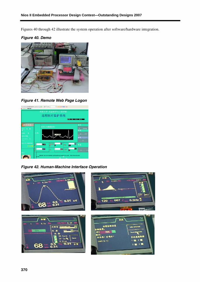
Figures 40 through 42 illustrate the system operation after software/hardware integration.
Figure 40. Demo
Figure 41. Remote Web Page Logon
Figure 42. Human-Machine Interface Operation
370
Portable Telemedicine Monitoring Equipment
Design FeaturesOur design has the following features:
■ Conception—While HHCE is becoming part of our lives, real home medical monitoring equipment is not available. HHCE is not effectively implemented because the existing portable monitoring equipment provides functions that are too simple or too expensive. Seeing this opportunity and feasibility, we chose to do the design. The Nios II processor gives our product superiority over its competitors in terms of size and price.
■ Function—The product is modern with competitive features, such as the simultaneous measurement of multiple parameters, high-capacity data storage, network communication, more signal processing algorithms to support more functions, etc. Meanwhile, its diversified functions prove the flexibility and high performance of the Nios II system.
■ Hardware design—SOPC techniques make our design simple and clear. We can complete each module independently and integrate them easily to form a system. We can embed several main devices (including the A/D converter and LCD IP blocks) for data transfer to reduce the CPU load while updating hardware modules rapidly. We can easily connect an IP block to the bus at the touch of a button, which was impossible for previous chip-based SOC systems. All IP blocks use the Avalon bus architecture and a unified synchronous clock.
■ Software algorithm—Our design is complex, including many modules and complicated algorithms. These difficulties are also features of our design. Algorithms such as waveform detection, data compression, and spectrum conversion are not fully applied in existing monitoring equipment. With these algorithms, our product will be more specialized, providing users more medical diagnosis methods and allowing them to enjoy medical treatment at home.
■ Upgrades—According to the requirements of different hospitals, communities, and homes, the multi-function, portable, medical monitoring system can be configured or upgraded quickly by selecting different front-end data acquisition modules and corresponding data processing CF cards without replacing the whole system platform.
■ Remote monitoring—The networking function enables more comprehensive monitoring. With the Internet, users can communicate remotely at any time. Doctors can monitor patients remotely through the network to determine the monitored patient’s health status while updating software or managing a database in real time. The Nios II protocol stack eased network development.
ConclusionWith this project, we gained a broader understanding of SOPC concepts and learned how to perform embedded development with the Nios II CPU. Altera’s SOPC solution provides a powerful design platform that allows us to develop hardware, drivers, and applications to develop systems rapidly and efficiently.
The two-month effort we put into the contest brought us the final design as well as more experience. We found the “real sense” of the design process, including IP cores, pre-simulation, post-simulation, and application optimization. Embedded development requires developers to have a systematic view and patience; program debugging is time-consuming but beneficial.
We found that design tools such as the embedded logic analyzer, SOPC Builder, C-to-Hardware Acceleration (C2H) Compiler, IDE, and DSP Builder accelerated our development. Although tasks differ, we learned how things relate and felt the power of teamwork.
After participating in the Nios II design contest several times, we are impressed with the Nios II processor’s flexibility and transparency, which distinguishes it from other embedded systems. We can
371
Nios II Embedded Processor Design Contest—Outstanding Designs 2007
see the full transparency from the bottom layer implementation to the application layer design, supporting better system design than any other embedded system.
Until now, we have had many problems to solve, for example, how to accelerate an interface switch, how to truly connect databases, how to improve the system’s DSP performance, and how to implement a more accurate biomedical signal waveform detection algorithm. These areas need our continuous efforts.
Finally, we would like to express our appreciation to all our teachers and classmates who helped us with the design, as well as our sincere gratitude to the host and judges of this contest. We will move ahead on our road of SOPC development.