MSP430 based microcontroller from Texas Instruments. MSP430 is developed by Texas Instruments as an extremely low power 16 bit architecture for use in low power, low cost, energy constrained embedded applicationsThe Hardware used is the MSP430 Launchpad from TI which contains a programmer/Debugger + two microcontrollers making it an ideal platform to start learning about MSP430G2xxx controller. Please note that this tutorial is a work in progress so new info will be added as it becomes available. Tutorial Overview In this tutorial,I will be focusing on MSP430G2553 which comes along with the Launchpad development kit.MSP430G2553 comes in a easy to use 20 pin DIP package with a 10 bit, 8 channel ADC,2 timers,1 UART,16KB Flash and 512 bytes of RAM.The code in the tutorial is written in embedded C and is compiled with an code limited version of IAR embedded workbench.You can also use Code Composer Studio from Texas Instruments.Before beginning I would recommend you to get a copy of the MSP430G2xxx user manual (slau144j.pdf) from TI website.It is better to print out the relevant sections of the usermanual for peripherals like ADC,timer uart etc so that you can easily browse through it. Ports of MSP430 Object 2 Object 3 0 Condividi Submitted by Rahul.Sreedharan on 7 June 2015 - 10:39am Object 1
Transcript
MSP430 based microcontroller from Texas Instruments.MSP430 is developed by Texas Instruments as an
extremely low power 16 bit architecture for use in low power, low cost, energy constrained embedded
applicationsThe Hardware used is the MSP430 Launchpad from TI which contains a programmer/Debugger +
two microcontrollers making it an ideal platform to start learning about MSP430G2xxx controller.
Please note that this tutorial is a work in progress so new info will be added as it becomes available.
Tutorial Overview
In this tutorial,I will be focusing on MSP430G2553 which comes along with the Launchpad development kit.MSP430G2553 comes in a easy to use 20 pin DIP package with a 10 bit, 8 channel ADC,2 timers,1 UART,16KB Flash and 512 bytes of RAM.The code in the tutorial is written in embedded C and is compiled with an code limited version of IAR embedded workbench.You can also use Code Composer Studio from Texas Instruments.Before beginning I would recommend you to get a copy of the MSP430G2xxx user manual (slau144j.pdf) from TI website.It is better to print out the relevant sections of the usermanual for peripherals like ADC,timer uart etc so that you can easily browse through it.
Ports of MSP430
Object 2
Object 3
0 Condividi
Submitted by Rahul.Sreedharan on 7 June 2015 - 10:39am
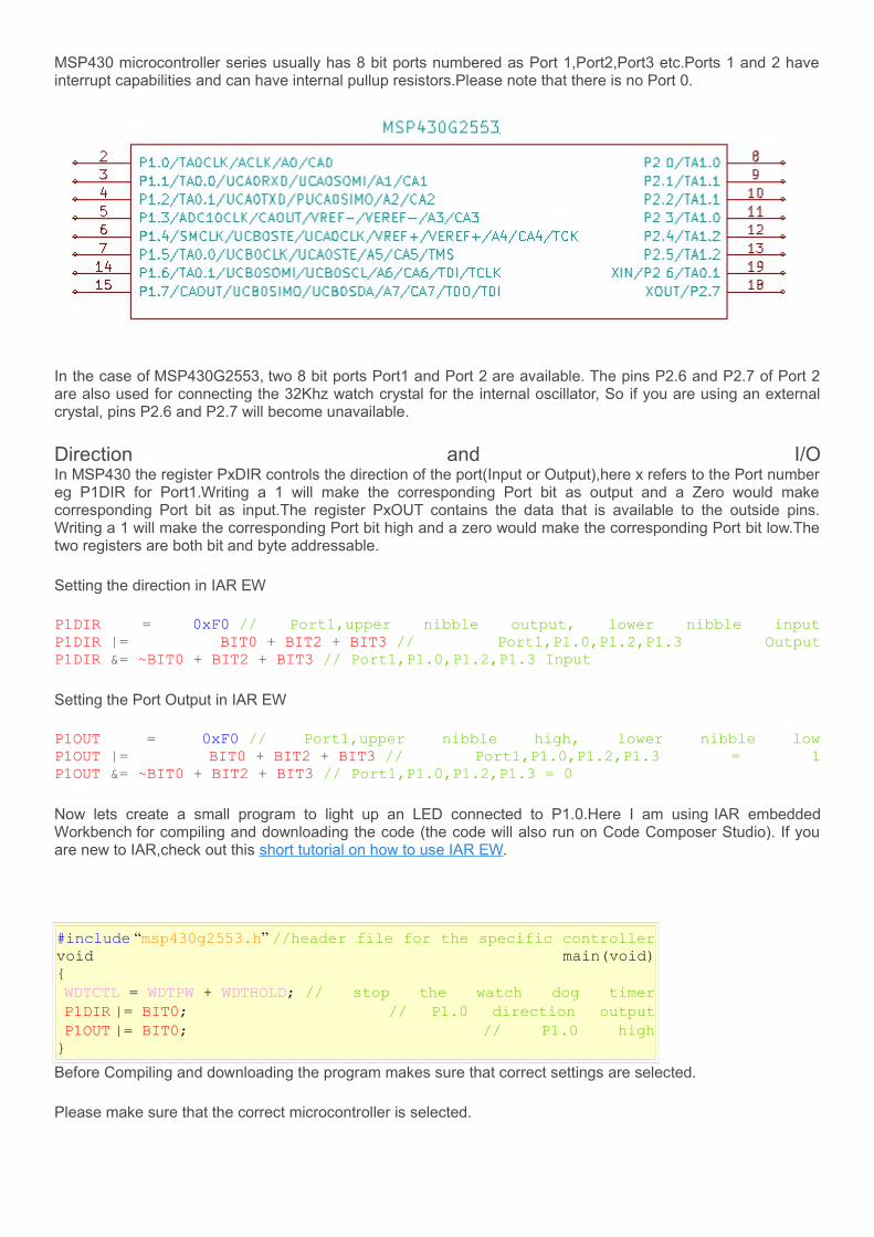
MSP430 microcontroller series usually has 8 bit ports numbered as Port 1,Port2,Port3 etc.Ports 1 and 2 have interrupt capabilities and can have internal pullup resistors.Please note that there is no Port 0.
In the case of MSP430G2553, two 8 bit ports Port1 and Port 2 are available. The pins P2.6 and P2.7 of Port 2 are also used for connecting the 32Khz watch crystal for the internal oscillator, So if you are using an external crystal, pins P2.6 and P2.7 will become unavailable.
Direction and I/OIn MSP430 the register PxDIR controls the direction of the port(Input or Output),here x refers to the Port number eg P1DIR for Port1.Writing a 1 will make the corresponding Port bit as output and a Zero would make corresponding Port bit as input.The register PxOUT contains the data that is available to the outside pins. Writing a 1 will make the corresponding Port bit high and a zero would make the corresponding Port bit low.The two registers are both bit and byte addressable.
Now lets create a small program to light up an LED connected to P1.0.Here I am using IAR embedded Workbench for compiling and downloading the code (the code will also run on Code Composer Studio). If you are new to IAR,check out this short tutorial on how to use IAR EW.
#include “msp430g2553.h” //header file for the specific controllervoid main(void){ WDTCTL = WDTPW + WDTHOLD; // stop the watch dog timer P1DIR |= BIT0; // P1.0 direction output P1OUT |= BIT0; // P1.0 high}
Before Compiling and downloading the program makes sure that correct settings are selected.
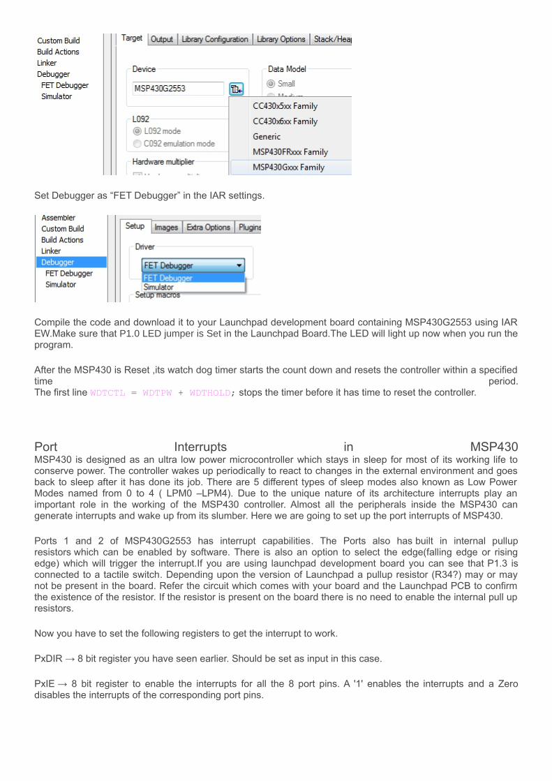
Please make sure that the correct microcontroller is selected.
Set Debugger as “FET Debugger” in the IAR settings.
Compile the code and download it to your Launchpad development board containing MSP430G2553 using IAR EW.Make sure that P1.0 LED jumper is Set in the Launchpad Board.The LED will light up now when you run the program.
After the MSP430 is Reset ,its watch dog timer starts the count down and resets the controller within a specified time period.The first line WDTCTL = WDTPW + WDTHOLD; stops the timer before it has time to reset the controller.
Port Interrupts in MSP430MSP430 is designed as an ultra low power microcontroller which stays in sleep for most of its working life to conserve power. The controller wakes up periodically to react to changes in the external environment and goes back to sleep after it has done its job. There are 5 different types of sleep modes also known as Low Power Modes named from 0 to 4 ( LPM0 –LPM4). Due to the unique nature of its architecture interrupts play an important role in the working of the MSP430 controller. Almost all the peripherals inside the MSP430 can generate interrupts and wake up from its slumber. Here we are going to set up the port interrupts of MSP430.
Ports 1 and 2 of MSP430G2553 has interrupt capabilities. The Ports also has built in internal pullup resistors which can be enabled by software. There is also an option to select the edge(falling edge or rising edge) which will trigger the interrupt.If you are using launchpad development board you can see that P1.3 is connected to a tactile switch. Depending upon the version of Launchpad a pullup resistor (R34?) may or may not be present in the board. Refer the circuit which comes with your board and the Launchpad PCB to confirm the existence of the resistor. If the resistor is present on the board there is no need to enable the internal pull up resistors.
Now you have to set the following registers to get the interrupt to work.
PxDIR → 8 bit register you have seen earlier. Should be set as input in this case.
PxIE → 8 bit register to enable the interrupts for all the 8 port pins. A '1' enables the interrupts and a Zero disables the interrupts of the corresponding port pins.
PxIES → 8 bit register to select the signal edge that would trigger the interrupt. A '1' means that interrupt will be triggered in the falling edge (high to low) and a Zero means that interrupt will be triggered in the rising edge(low to high).
PxIFG → 8 bit flag register which shows which pin has triggered the interrupt.
PxREN → 8 bit flag register which enables the pull up resistors of the Port Pins.
Now lets create a small program that would toggle the LED connected to P1.0 to toggle when the switch connected to the P1.3 is pressed.In this case I am using the tactile switch connected to P1.3 of MSP430G2553 to trigger the interrupt. The port pin P1.3 is pulled up to VCC(3V) by enabling the nternal pull up resistors (if there is an external pullup resistor, there is no need to use the internal ones) and a high to low transition is selected to trigger the port interrupt.
_BIS_SR(LPM0_bits + GIE); //enter LPM0 with interrupts enabled}
The above program shows how to initialize the port P1.3 to get the interrupt mode working.After the initialization is complete we put the controller in sleep mode more specifically in LPM0 mode withinterrupts enabled using_BIS_SR(LPM0_bits + GIE);
In LPM0 mode the CPU and clock to the CPU (MCLK) is disabled while the clocks to the peripherals (SMCLK and ACLK) are active.
GIE is a bit inside the Status Register (SR) of the MSP430 processor core. It is used to enable or disable the maskable interrupts of the MSP430.If this bit is not set the P1.3 interrupt will not happen. Sometimes people will configure everything and forget to set the GIE bit and then start hunting through myriad of register options to troubleshoot the problem.
Please note that GIE bit is used to control all the maskable interrupts of the MSP430.The Status Register is also used to put the MSP430 in various Low Power Mode's like LPM0, LPM1, LPM2 etc. MSP430 can enter various Low Power Mode's by configuring various registers like CPUOFF, OSCOFF in the Status Register. Instead of individually setting the bits we can use the compiler directive LPM0_bits to achieve the same(here we are putting the controller in LPM0).A detailed explanation of Low Power Modes is present in the user manual of the respective controller along with the power consumption data for each modes.
When an interrupt happens processor wakes up from the Low power mode and goes to the interrupt vector location. If you are coding using assembly language you have to provide the address of the location in hex. Since we are using C, we can do it as
#pragma vector = PORT1_VECTOR__interrupt void Port1(void){ P1IFG &= ~BIT3; //clear P1IFG P1OUT ^= BIT0; //toggle LED at P1.0}
Here PORT1_VECTOR is the interrupt vector location, It is defined in the header file “msp430g2553.h” if you open the file you can see the memory location corresponding to the PORT1_VECTOR. void Port1(void) is the user defined name for the interrupt service routine.
When an interrupt happens the corresponding flag in P1IFG register is set(here BIT3 of P1IFG), You should clear the flag immediately inside the interrupt service outine.
P1IFG &= ~BIT3;
After that you can toggle the LED connected to the P1.0 by xoring BIT0 of P1OUT.
Selecting the PinsIn MSP430 the port pins are shared among various peripherals like ADC inputs, Timers,Comparator inputs etc. To select the various functions associated with the same pins MSP430has two 8 bit registers called PxSEL and PxSEL2.Not all functions requires you to configure the PxSEL and PxSEL2 register, some times selecting or activating the peripheral would automatically configure the pins for eg ADC.In other cases like enabling I2C or Capacitive touch sensing you have to explicitly configure the PxSEL registers to enable the pins for performing that function.The information on how to configure the port selection registers is present in the datasheet of the controller .In MSP430G2553 that table is buried in the Port Schematics section at the end of the whole datasheet. Here is a sample of the Pin Selection table of MSP430g2553.
Interfacing 7 Segment LED Display with MSP430 Launchpad
Submitted by Rahul.Sreedharan on 19 June 2015 - 7:05pm
In this tutorial we will learn to interface a 7 segment LED display (LT543) with MSP430 Launchpad development board from Texas Instruments.A 7 Segment LED dispaly can be used to display a limited number of character sets like numbers(0-9),Hexadecimal characters (0-F) and a few english characters(H,L,E etc) but being a LED segment it can be easily read in the dark and is used widely on instrument panels and industrial displays.
Source Code and Circuit Diagram
All the C soure files along with datasheets and ciruit diagram used in this tutorial can be downloaded from our
GitHub Page.
The code is written in embedded C and compiled using IAR Embedded Workbench.If you are new to Github
Check this article to download code .
Circuit Diagram for interfacing 7 segment LED Display with MSP430 Launchpad can be found here.
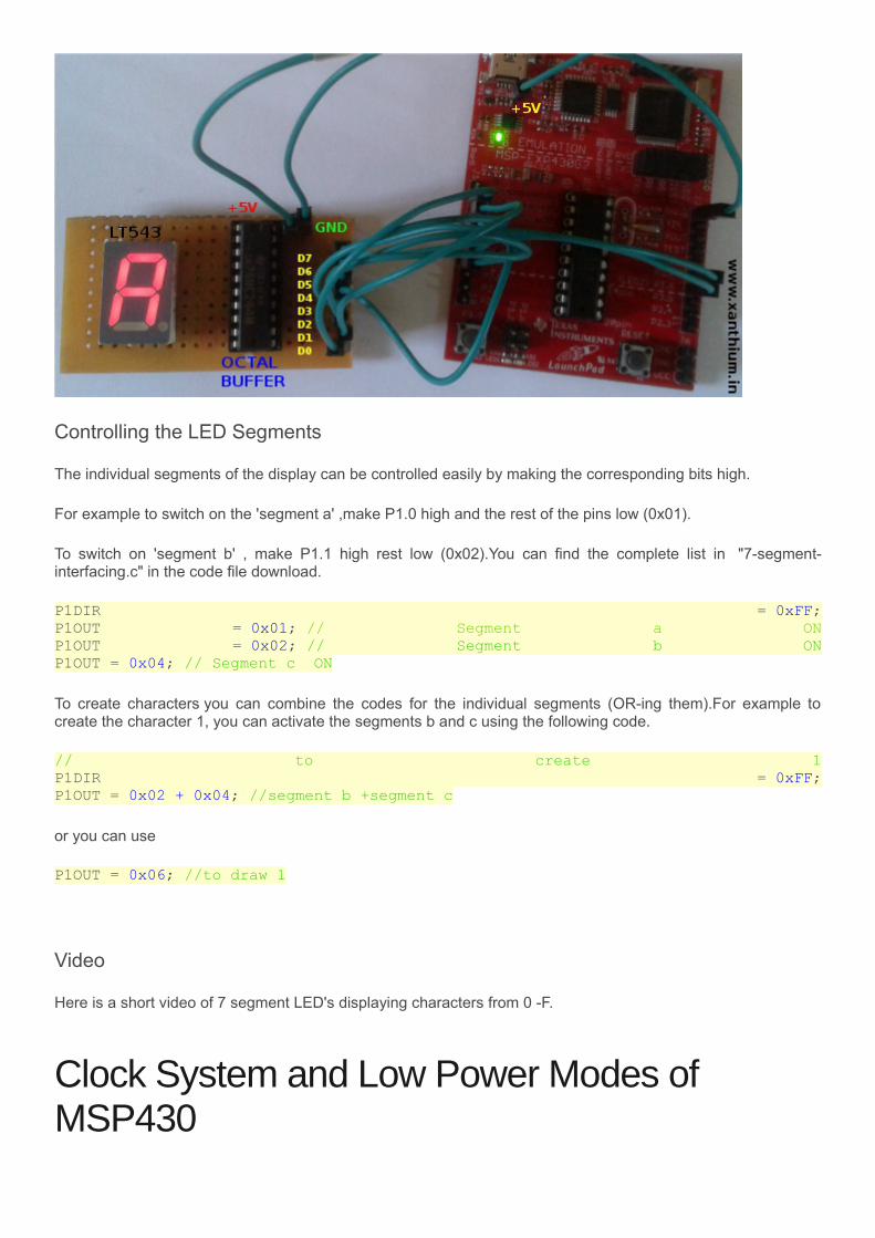
To interface the 7 segment to the MSP430 launchpad ,we are going to build a small interfacing circut using 74LS244 octal buffer chip.LED's tend to draw a lot of current so to be on the safer side i am putting a buffer between the MSP430G2553 pins and the 7 Segment LED pins.The circuit diagram of the interfacing circuit is shown below.The PDF version of the circuit can be downloaded from here.
The 7 Segment LED display i am using here is LT543 which is a common cathode LED display(negative terminal of all the LED segments in the display are made common,Pins 3 and 8) .The pin diagram and the segments of the LT543 are shown below. Here pin numbers 3 and 8 are the common cathode and has to be tied to ground.
The pin numbers are shown in black and the LED segments associated with it are shown in red
The Octal buffer 74LS244 runs on 5V which you can take it from the USB section of the launchpad board as shown in the figure below.
Here i am using Port 1 of MSP430G2553 to interface with 7 Segment display.P1.0 is connected to segment a of the LED display,P1.1 to segment b,............and P1.7 to segment dp.Segment a is available at Pin Number 1 of connector P2 (data),Segment b at Pin Number 2 and so on.
Controlling the LED Segments
The individual segments of the display can be controlled easily by making the corresponding bits high.
For example to switch on the 'segment a' ,make P1.0 high and the rest of the pins low (0x01).
To switch on 'segment b' , make P1.1 high rest low (0x02).You can find the complete list in "7-segment-interfacing.c" in the code file download.
P1DIR = 0xFF;P1OUT = 0x01; // Segment a ONP1OUT = 0x02; // Segment b ONP1OUT = 0x04; // Segment c ON
To create characters you can combine the codes for the individual segments (OR-ing them).For example to create the character 1, you can activate the segments b and c using the following code.
// to create 1P1DIR = 0xFF;P1OUT = 0x02 + 0x04; //segment b +segment c
or you can use
P1OUT = 0x06; //to draw 1
Video
Here is a short video of 7 segment LED's displaying characters from 0 -F.
Clock System and Low Power Modes of MSP430
Object 8
Object 9
2 Condividi
Submitted by Rahul.Sreedharan on 7 June 2015 - 9:10am
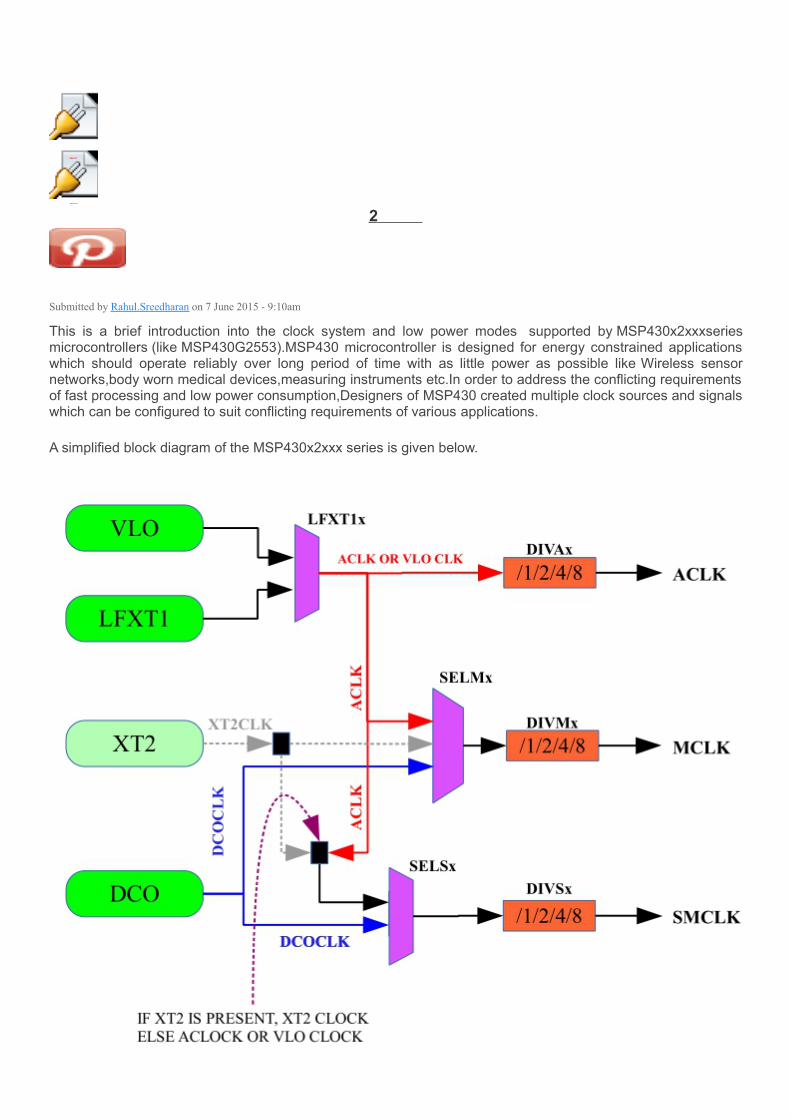
This is a brief introduction into the clock system and low power modes supported by MSP430x2xxxseries microcontrollers (like MSP430G2553).MSP430 microcontroller is designed for energy constrained applications which should operate reliably over long period of time with as little power as possible like Wireless sensor networks,body worn medical devices,measuring instruments etc.In order to address the conflicting requirements of fast processing and low power consumption,Designers of MSP430 created multiple clock sources and signals which can be configured to suit conflicting requirements of various applications.
A simplified block diagram of the MSP430x2xxx series is given below.
Basic Clock System provides the required clocks to the MSP430x2xxx devices.Most MSP430 microcontrollers have 4 clock sources to produce fast and slow clocks.The main clock sources (oscillators) of MSP430x2x family are
LFXT1CLK - It is a crystal powered low/high frequency oscillator that can work with either a 32KHz standard watch crystal,standard crystals that operate in the MHz range or external clock sources (400KHz -16MHz range).Please note that,not all clock features are supported on all msp430x2xxx devices.For eg: LFXT1CLK of MSP430G2553 supports only the low frequency mode.You can only connect a 32KHz watch crystal to the oscillator inputs,higher frequency crystals are not supported.
XT2CLK -This is an optional high frequency oscillator that can be used with standard crystals,resonator or external clock sources in the 400KHz to 16MHz range.Please note that XT2 is absent in MSP430Gxxx series like MSP430G2553.
DCOCLK - DCO is an integrated Digitally Controlled Oscillator which do not use any external crystals.The DCO can generate a wide variety of frequencies ranging from few 100 kilo hertz to 10's of MHz.The oscillator has a first startup time and is the default clock of the MSP430 after reset.One problem with DCO is that clock frequency is temperature dependent.
VLOCCLK - this is a very low power/low frequency internal oscillator than can produce a frequency of 12 KHz.
Clock Signals of MSP430
MSP430 produces 3 different clock signals using a combination of the above mentioned oscillators.These clock signals can be routed to various peripherals like CPU,Timers,ADC etc depending upon the requirements.The 3 clock signals are
MCLK - Known as Main Clock.It is a fast,high frequency clock usually used by the CPU or other fast components like ADC10,ADC12,Watch Dog Timer (WDT).MCLK can be sourced either from LFT1CLK,DCO,VLO or XT2 oscillator (if it is present).You can divide the clock signal by 1/2/4/8 using the internal divider.
SMCLK - Known as Sub Main clock.It can be sourced either from LFT1CLK,DCO,VLO or XT2 oscillator (if it is present).You can divide the clock signal by 1/2/4/8 using the internal divider.
ACLK - Known as Auxiliary Clock is a slow, low frequency clock(12 KHz or 32KHz).It can only be sourced from LFT1CLK or VLO.You can divide the clock signal by 1/2/4/8 using the internal divider. ACLK is active in all Low power modes except LPM4.
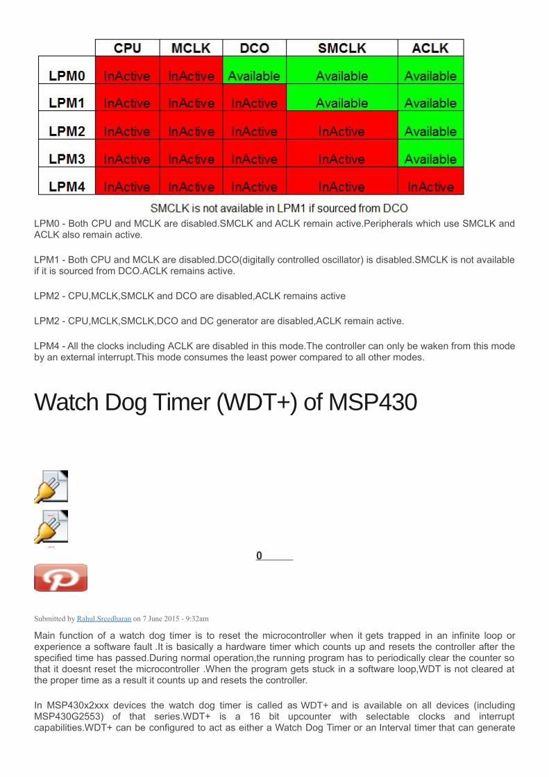
Low Power Modes of MSP430
To conserve power, MSP430 spends most of its time in sleep and periodically wakes up to perform some operation and again goes back to sleep.MSP430 has 5 low power modes named as LPM0 to LPM4 .The table below shows which clocks are active and which are disabled in various low power modes.
LPM0 - Both CPU and MCLK are disabled.SMCLK and ACLK remain active.Peripherals which use SMCLK and ACLK also remain active.
LPM1 - Both CPU and MCLK are disabled.DCO(digitally controlled oscillator) is disabled.SMCLK is not available if it is sourced from DCO.ACLK remains active.
LPM2 - CPU,MCLK,SMCLK and DCO are disabled,ACLK remains active
LPM2 - CPU,MCLK,SMCLK,DCO and DC generator are disabled,ACLK remain active.
LPM4 - All the clocks including ACLK are disabled in this mode.The controller can only be waken from this mode by an external interrupt.This mode consumes the least power compared to all other modes.
Watch Dog Timer (WDT+) of MSP430
Object 11
Object 12
0 Condividi
Submitted by Rahul.Sreedharan on 7 June 2015 - 9:32am
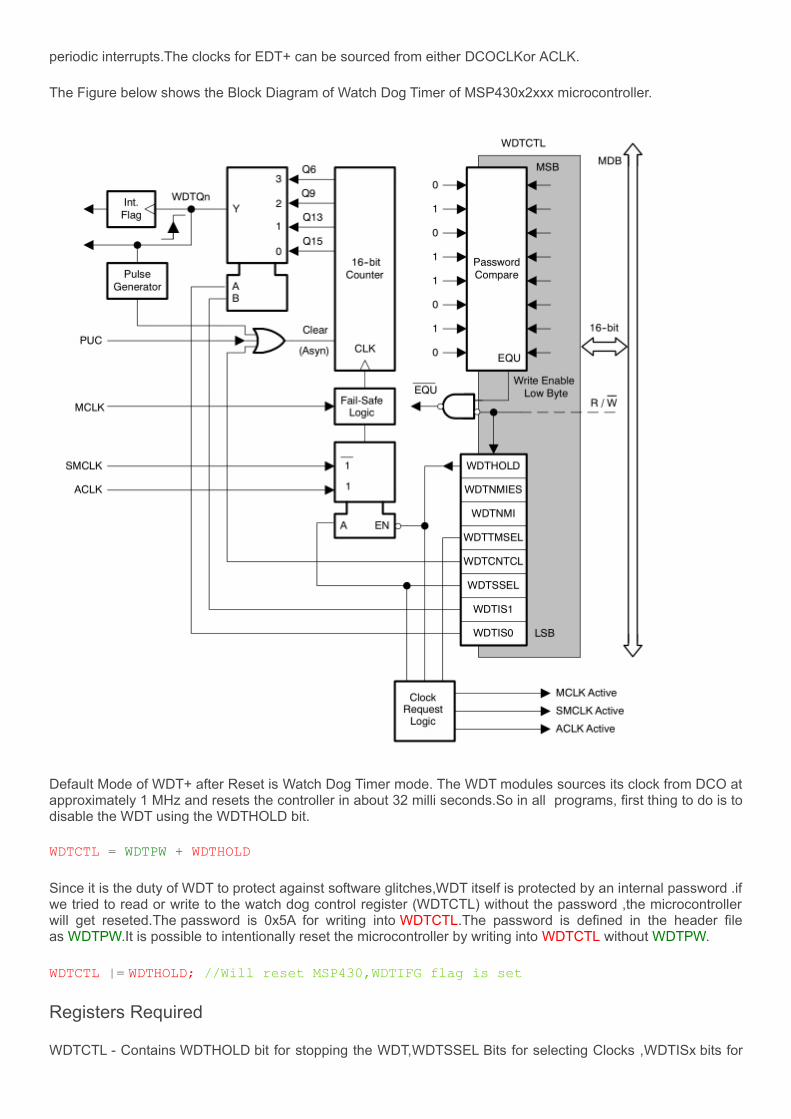
Main function of a watch dog timer is to reset the microcontroller when it gets trapped in an infinite loop or experience a software fault .It is basically a hardware timer which counts up and resets the controller after the specified time has passed.During normal operation,the running program has to periodically clear the counter so that it doesnt reset the microcontroller .When the program gets stuck in a software loop,WDT is not cleared at the proper time as a result it counts up and resets the controller.
In MSP430x2xxx devices the watch dog timer is called as WDT+ and is available on all devices (including MSP430G2553) of that series.WDT+ is a 16 bit upcounter with selectable clocks and interrupt capabilities.WDT+ can be configured to act as either a Watch Dog Timer or an Interval timer that can generate
periodic interrupts.The clocks for EDT+ can be sourced from either DCOCLKor ACLK.
The Figure below shows the Block Diagram of Watch Dog Timer of MSP430x2xxx microcontroller.
Default Mode of WDT+ after Reset is Watch Dog Timer mode. The WDT modules sources its clock from DCO at approximately 1 MHz and resets the controller in about 32 milli seconds.So in all programs, first thing to do is to disable the WDT using the WDTHOLD bit.
WDTCTL = WDTPW + WDTHOLD
Since it is the duty of WDT to protect against software glitches,WDT itself is protected by an internal password .if we tried to read or write to the watch dog control register (WDTCTL) without the password ,the microcontroller will get reseted.The password is 0x5A for writing into WDTCTL.The password is defined in the header file as WDTPW.It is possible to intentionally reset the microcontroller by writing into WDTCTL without WDTPW.
WDTCTL |= WDTHOLD; //Will reset MSP430,WDTIFG flag is set
Registers Required
WDTCTL - Contains WDTHOLD bit for stopping the WDT,WDTSSEL Bits for selecting Clocks ,WDTISx bits for
selecting the timer interval,
IE1 - Contains WDTIE used to enable the interrupt in interval timer mode
IFG1 - WDTIFG flag which is set when WDT expires in watch dog mode.
Please note that only the important bits are shown,Please refer the datasheet for more details.
WDT+ as an Interval Timer
WDT+ can operate in two modes,one of the mode is called as interval timer mode .In this mode WDT+ generates an interrupt after a specified amount of time(MSP430 is not reseted in this mode).
The mode selection is done by setting the WDTTMSEL bit in WDTCTL register (WDTTMSEL = 1).You can also select the clocks(ACLK or SMCLK) to be used by WDT in this mode by configuring the WDTSSEL bit.The interval time period can be set by configuring WDTISx bits of WDTCTL.
Instead of going through all these bit fields ,you can use the interval time period constants defined in the header file "msp430g2553.h".
WDT_MDLY_32 means that time period of the interval is 32 milliseconds and the clock is taken from SMCLK.
WDT_ADLY_1000 means that time period of the interval is 1000 milliseconds (1Second) and the clock is taken from ACLK.
The details are provided next to the constants in comments(which is not shown in the above image ).Now lets write a small program to blink the LED after 1 second interval.The Clocks for WDT+ (interval timer mode ) are taken from ACLK.
#include "msp430g2553.h"void main(void){ WDTCTL = WDTPW + WDTHOLD;//Stop the WDT to prevent reset P1DIR |= BIT0; //P1.0 output P1OUT &= ~BIT0; //P1.0 = 0 WDTCTL = WDT_ADLY_1000; //using ACLK from the LFXT1CLK IE1 |= WDTIE; //Enable the WDTIE bit _BIS_SR(LPM3_bits + GIE); //Go to LPM3 with interrupts enabled}
Please make sure that your launchpad has the watch crystal soldered to XIN and XOUT pin of MSP430G2553.You can source the clock from other sources like SMCLK but time interval will be short,also we are going to LPM3 in which SMCLK is disabled.
In the first line like all programs,we first stop WDT from reseting the MSP430 controller.Then we configure the port pin P1.0 to light up the LED.
We then configure the WDT to go into the interval timer mode by using one of the constants from the header file
WDTCTL = WDT_ADLY_1000
Here we have decided to make the interval as 1000 milli seconds or 1 second.The clock for WDT interval timer is sourced from ACLK as we are planning to go to sleep in LPM3.
After configuring the WDTCTL register we enable the WDT timer interrupt in IE1 .
IE1 |= WDTIE;
Then we put the processor in sleep mode LPM3 (only ACLK is active i this mode ) with GIE enabled and wait for the WDT interrupt to come.
Here WDT_VECTOR is the interrupt vector location.The P1.0 is toggled inside the ISR to blink the LED every 1 second.WDTIFG is cleared automatically as interrupt is processed in this mode.
WDT+ as Watch Dog Timer
The main job of the Watch dog timer is to reset the microcontroller when it experiences a software fault like getting into an infinite loop.The WatchDog prevents run away code execution and helps to put the controller in a known situation.
The mode selection is done by clearing the WDTTMSEL bit in WDTCTL register (WDTTMSEL = 0).Like the previous example (interval timer mode), it is much better to use the timer constants defined in the header file.The Timer constants of Watch dog mode are defined separately in the header file.
Like the interval timer mode,clock to the Watch dog timer can be sourced either from either ACLK orSMCLK.
Here WDT_ARST_1000 means that WDT will reset the microcontroller in 1000 milliseconds and uses the ACLK .while WDT_MRST_32 means that WDT will reset the microcontroller in 32 milliseconds and uses the SMCLK.
Now let's write a small program to illustrate the use of Watch dog timer.In this example a infinite " while(1) " loop is used to simulate a software glitch.
#include "msp430g2553.h"void main(void){ WDTCTL = WDTPW + WDTHOLD;// Stop the WDT to prevent reset int i; // Count value for delay P1DIR |= BIT0 + BIT6; // P1.0(Red) and P1.6(Green)output P1OUT &= ~BIT0 + BIT6 ; // P1.0 = 0,P1.6 =0 for(i =0;i<0xffff;i++); // A Small delay P1OUT |= BIT0; // P1.0 = 1(Red LED On) WDTCTL = WDT_ARST_1000; // Put WDT+ in Watch Dog Mode
//while(1); // used to simulate glitch
WDTCTL = WDT_ARST_1000; // Reset WDT+ for another 1 second, P1OUT |= BIT6; // Switch on green LED WDTCTL = WDTPW + WDTHOLD;// Stop WDT _BIS_SR(LPM0); // Put the CPU to sleep}
In this program at first the WDT is halted using
WDTCTL = WDTPW + WDTHOLD;
so that we could configure the ports properly.The ports P1.0 (Red LED) and P1.6 (Green LED) are configured as outputs to light up the LED's on the Launchpad board. After that a small delay is provided to blink the red LED connected to P1.0.
Then the WDT is started in watch dog mode for a 1 second duration using
WDTCTL = WDT_ARST_1000;
Now to simulate a software glitch ,I am using an infinite while loop.
Under normal circumstances,ie when " while(1); " is commented out as shown in the above code.The flow of execution proceeds in a linear function and clears the watchdog timer using
WDTCTL = WDT_ARST_1000;
for another 1 second preventing a system reset.The code then lights up the green LED and stops the WDT.
When " while(1); " is uncommented and compiled into the program to simulate a glitch.The program would enter into an infinite loop after enabling the WDT.The CPU will be trapped in the loop while WDT slowly counts up.When the prescribed time period is up WDT resets the CPU and code execution starts again from the beginning (Red LED will start blinking).
In real world conditions most problems can be solved by a system reset So next time the code will not enter into the infinite loop and the execution proceeds to light up the green LED.
In our case RESETing the controller will not force the controller out of loop since " while(1); " loop is hard coded by me and not a software glitch.
After the watch dog timer has reseted the processor the WDTIFG flag in IFG1 will be set.Your code can then use that information to notify that system have been reseted by WDT
ADC10 Tutorial for MSP430 Launchpad
Object 14
Object 15
3 Condividi
Submitted by Rahul.Sreedharan on 16 October 2015 - 7:57am
In this section we will learn how to configure and use the ADC10 of MSP430G2XX3 microcontroller that comes with the TI Launchpad development board. Later we will configure the internal temperature sensor of MSP430 and display the value on a 16X2 LCD module.
MSP430G2xxxx series (for eg MSP430G2553) comes with a 10 bit Successive Approximation ADC that can operate at 200Ksps. The ADC10 of MSP430G2xxx3 comes with 8 analog channels which can be used for interfacing external sensors and two internal one (one for Internal temperature sensor and the other for measuring Vcc-Vss/2 ).The ADC 10 also has a built in software selectable voltage reference source (1.5V or 2.5V) along with provision for providing external references.
All the C source files used in this tutorial for configuring ADC10 can be downloaded from our GitHub Page.
If you are new to Github Check this article to download code .
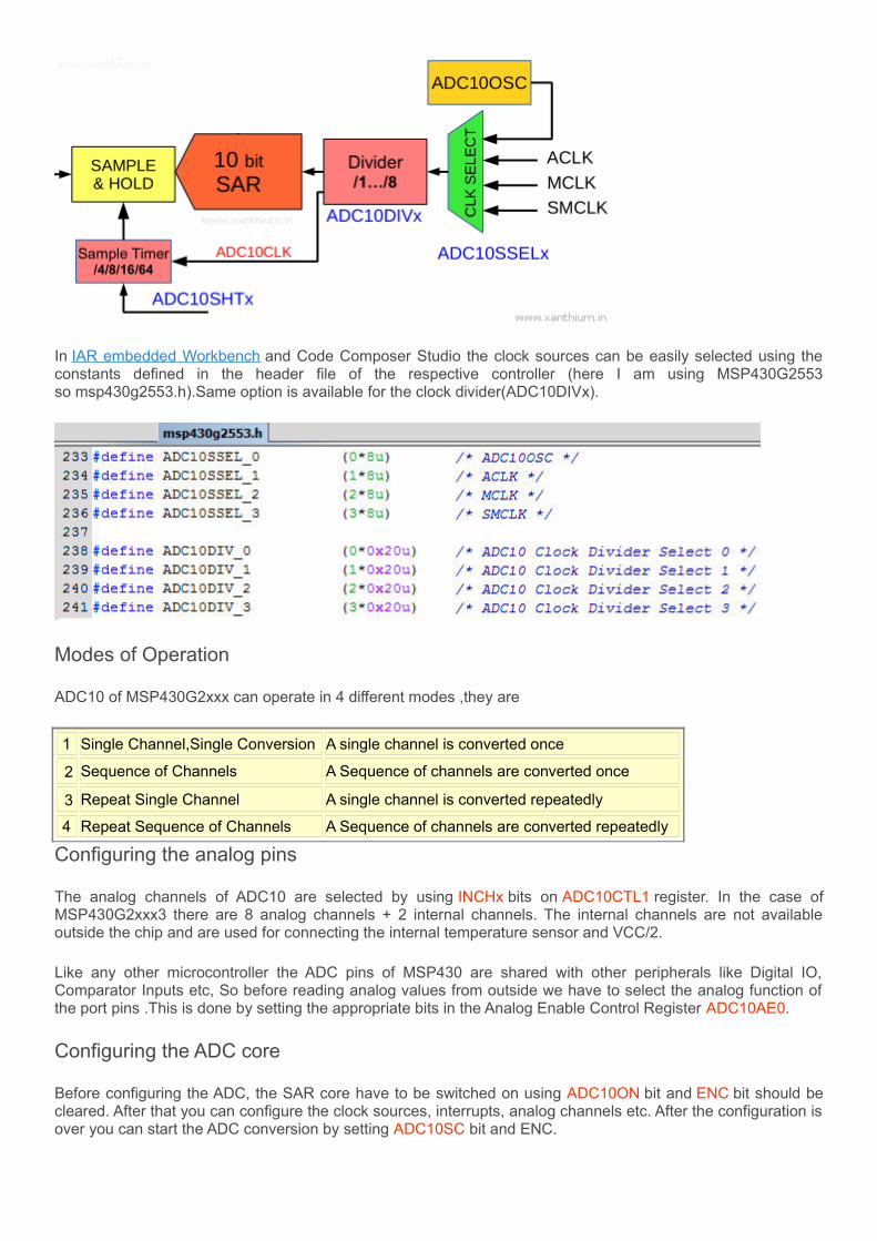
Block Diagram of ADC10
Clock Sources
The SAR core of the MSP430G2xxx3 microcontroller can be clocked by either ACLK, SMCLK,MCLK or by the internal Oscillator ADC10OSC.The clock produced by the internal oscillator ADC10OSC is in the range of 5MHz and varies with changes in temperature and Voltage. The default clock for ADC10 is taken from ADC10OSC .
ADC10SSELx bits on ADC10CTL register is used to select the clock source. The selected clock can be divided by using ADC10DIVx bits (on ADC10CTL) before giving to the SAR core. The clock coming after the Divider is called ADC10CLK and is also used for setting Sample and Hold Timing.
In IAR embedded Workbench and Code Composer Studio the clock sources can be easily selected using the constants defined in the header file of the respective controller (here I am using MSP430G2553 so msp430g2553.h).Same option is available for the clock divider(ADC10DIVx).
Modes of Operation
ADC10 of MSP430G2xxx can operate in 4 different modes ,they are
1 Single Channel,Single Conversion A single channel is converted once
2 Sequence of Channels A Sequence of channels are converted once
3 Repeat Single Channel A single channel is converted repeatedly
4 Repeat Sequence of Channels A Sequence of channels are converted repeatedly
Configuring the analog pins
The analog channels of ADC10 are selected by using INCHx bits on ADC10CTL1 register. In the case of MSP430G2xxx3 there are 8 analog channels + 2 internal channels. The internal channels are not available outside the chip and are used for connecting the internal temperature sensor and VCC/2.
Like any other microcontroller the ADC pins of MSP430 are shared with other peripherals like Digital IO, Comparator Inputs etc, So before reading analog values from outside we have to select the analog function of the port pins .This is done by setting the appropriate bits in the Analog Enable Control Register ADC10AE0.
Configuring the ADC core
Before configuring the ADC, the SAR core have to be switched on using ADC10ON bit and ENC bit should be cleared. After that you can configure the clock sources, interrupts, analog channels etc. After the configuration is over you can start the ADC conversion by setting ADC10SC bit and ENC.
The ADC conversion can be started by software or by hardware. In Software ,the conversion is started by setting the ADC10SC bit by the program. In Hardware, the conversion is started by an external peripheral like Timer A ,this method is recommended if there are time and power constraints.
ADC10 Interrupts
After the conversion is finished the ADC10 sets the ADC10IFG flag and an interrupt is generated. The converted value is available in the ADC10MEM register for further processing. The ADC10IFGflag is automatically reset after the interrupt is processed. Please note that for the interrupt to occur the ADC10IE flag and GIE bit should be set.
Writing the Code
Now let's write a small program to configure the ADC and convert analog values generated by a potentiometer. The program will use Single Channel, Single conversion and convert the voltage levels of a potentiometer attached to the analog channel A0 of MSP430G2553 chip (Pin number 2) on Launchpad board.
The circuit diagram for connecting the Launchpad is shown below along with the image. The central pin of the pot is connected to the A0 pin of MSP430G2553.
Now type the following code into IAR or CCS IDE and compile.
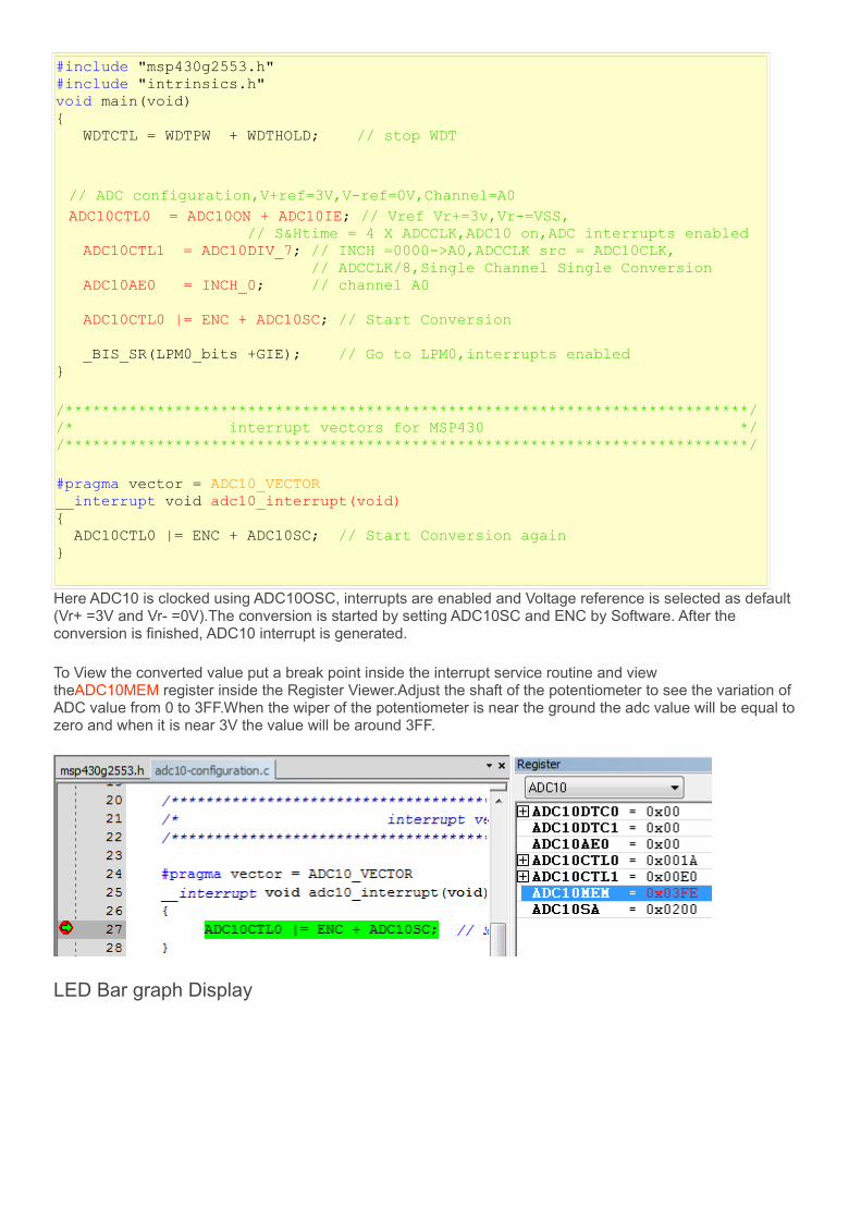
Here ADC10 is clocked using ADC10OSC, interrupts are enabled and Voltage reference is selected as default (Vr+ =3V and Vr- =0V).The conversion is started by setting ADC10SC and ENC by Software. After the conversion is finished, ADC10 interrupt is generated.
To View the converted value put a break point inside the interrupt service routine and view theADC10MEM register inside the Register Viewer.Adjust the shaft of the potentiometer to see the variation of ADC value from 0 to 3FF.When the wiper of the potentiometer is near the ground the adc value will be equal to zero and when it is near 3V the value will be around 3FF.
LED Bar graph Display
Here we are going to implement a bar graph style display to show the ADC values using MSP430 Launchpad and a couple of LED’s. The bar graph display consists of 8 LED's arranged linearly and connected to Port 2 of the MSP430G2553 chip.
When the ADC value is Maximum ie 0xFE all the 8 LED's will light up and when ADC value is above10, only one will glow. By varying the potentiometer connected to the A0 input of MSP430 you can vary the number of LED's lighting up.
One thing to note is that, P2.6 and P2.7 of MSP430G2553 will behave as Crystal input/output (XIN/XOUT) by default. In order to put the pins in digital IO mode their respective bits in P2SEL and P2SEL2 should be cleared.
The circuit diagram is shown below.
The code converts the analog value available at A0 input into its equivalent digital value.After the conversion an "if " ladder in the Interrupt Service Routine decides which LED's to light up.
Timer A of MSP430
Object 17
Object 18
0 Condividi
Submitted by Rahul.Sreedharan on 10 June 2015 - 7:21pm
MSP430 series chips have two types of Timers known as Timer_A and Timer_B. Both of them are 16 bit timers with several capture compare channels and selectable clock sources. Timer_B is slightly complex than Timer_A and offers more extensive interrupt capabilities and capture compare channels.
MSP430Gxxx series chips that ship with Launchpad development board usually have two Timer_A modules named as Timer0_A3 and Timer1_A3.Here A3 indicates the number of Capture Compare registers (here 3 registers) available in each timer.Timer A is a 16 bit Timer/Counter with 3 capture compare registers.
Block Diagram
Block Diagram of Timer_A simplified
The Timer can be clocked either by SMCLK, ACLK,TACLK or INCLK. If you are not familiar with SMCLK or ACLK,You can check out the Clock system of MSP430 here.
SMCLK is an internal clock generally taken from DCO (Digitally Controlled Oscillator) and is in the Megahertz range. The DCO clock is temperature dependent and may change depending upon temperature.
ACLK is an internal clock taken either from VLO or an external 32KHz clock crystal connected to the MSP430.ACLK when taken from an external clock crystal is usually stable and do not change with temperature. The ACLK frequency is usually in Kilo hertz range (32KHz).
TACLK and INCLK are external clocks that can be connected to MSP430 through external pins.
TASSELx bits are used to select the required clock to the 16 bit Timer register and IDx bits are used to select clock divider which are present in the TACTL register.
The 16 bit Timer A register(TAR) starts counting on the positive edge of the clock. TAR can be cleared by setting the TACLR bit to 1.
Timer_A has 4 operating modes selected by the MCx bits in TACTL register.
MCx = 00 – Timer is halted and Timer stops counting.
MCx = 01 – Timer is started in the Up Mode.
MCx = 10 – Timer is started in Continuous Mode.
MCx = 11 – Timer is started in Up/Down Mode
Timer A Interrupts
Timer A in MSP430 have two interrupt vector locations,one for TACCR0 and the other for rest of the channels as well as the Timer overflow (TAIFG).
The register TACCR0 has a separate vector location which has a higher priority compared to the other timer interrupts.
In IAR embedded workbench, It is defined as TIMER0_A0_VECTOR for Timer0_A3 and asTIMER1_A0_VECTOR for Timer1_A3 in the header file (msp430g2553.h).
Rest of the capture compare channels (CCR1 and CCR2) along with the Timer overflow (TAIFG) are given separate vector location . Since all of them are combined together the interrupt vector register TAIV is used to determine which flag requested an interrupt.
In IAR embedded workbench,It is defined as TIMER0_A1_VECTOR for Timer0_A3 and asTIMER1_A1_VECTOR for Timer1_A3 in the header file (msp430g2553.h).
To identify which flag caused the interrupt it is recommended to use a switch structure like this inside the ISR.
switch(TAIV){ case 0x002: // CCR1 interrupt comes here break;
case 0x004: //CCR2 interrupt comes here break;
case 0x00A: //TAR overflow interrupt comes here break;}
Continuous Mode (MCx = 10)
In Continuous Mode ,the timer repeatedly counts up to 0FFFFh and restarts from zero. When the Timer overflows TAIFG flag is set and an interrupt is generated if TAIE bit is set.
Now lets write a small program to blink an LED connected to P1.0 of MSP430G2553 (Launchpad board) whenever TAR overflows. I am using IAR embedded workbench and launchpad development platform. Create a new C Project in IAR and compile the code given below.
_BIS_SR(LPM0_bits + GIE); // Sleep in LPM0 with interrupts enabled}
#pragma vector = TIMER0_A1_VECTOR //Timer0,TAIFG interrupt vector__interrupt void TimerA(void){ switch(TAIV) { case 0x002: // CCR1 not used break; case 0x004: //CCR2 not used break; case 0x00A: P1OUT ^= BIT0; //TAR overflow interrupt break; }}
In the above code we are using the ACLK sourced from a 32KHz watch crystal to provide clock to the timer module.
TASSEL_1 is a constant defined in msp430g2553.h file which is used to select the Timer Clock as ACLK. You can also individually set the TASSELx bits but TASSEL_1 makes life easier for the programmer.
ID_2 is used to set the clock divider here ACLK/4 ,So 32KHz/4 = 8KHz which would give the time period at 0.125ms.
TAIE is used to enable the timer overflow interrupt(maskable).
After the above parameters are configured in the TACTL register ,we start the timer in Continuous mode by setting MCx =10.TACTL |= MC_2and put the CPU in low power mode (LPM0) with interrupts enabled.
The TAR starts to run and overflows in about 8 seconds (0.125ms *65536).The TAIFG flag is set and the code reaches the ISR for Timer0 and toggles the LED connected to P1.0.
When going into the Low Power Modes Please remember the clocks which will be disabled in that Low Power Mode.For eg you are using SMCLK to trigger your Timer A and you decides to put the micro controller into LPM3.In LPM3 SMCLK is disabled, Timer A will not update itself and your timer and the peripherals triggered by it stays dead. Also remember to enable the GIE bit when going into LPM.
Configuring CCRx interrupts
In Continuous mode you can also set the interrupts for other channels like CCR0,CCR1 and CCR2.You have to enable the interrupt enable bits for the corresponding registers and load the values in to the capture compare registers.
In the code snippet shown below ,we are using SMCLK instead of ACLK by setting theTASSEL_2 bits .Here i am showing only the timer configuration code segment you can find the full code in the zip file.
Here we are configuring all the capture compare registers(CCR) as well as the timer overflow interrupt.We enable the TAIFG interrupt in TACTL first and then load all the CCR registers with the count value.After that CCR interrupts for the respective registers are enabled and counter is started in continuous mode.
TACTL |= MC_2; // Start the timer in continuous mode
_BIS_SR(LPM0_bits + GIE); // Sleep in LPM0 with interrupts enabled
When the Timer register counts and reaches the value 10000 ,CCR0 interrupt is triggered and the program control goes to the CCR0 interrupt routine of Timer 0.You can then lit up an LED or do something.
#pragma vector = TIMER0_A0_VECTOR //CCR0 interrupt vector__interrupt void CCR0_Interrupt(void){ P1OUT ^= BIT0; //toggle an LED }
When TAR reaches the count = 30000 the CCR1 interrupt is triggered,CCR2 interrupt is triggered at40000 and finally the timer overflow (TAIFG) is triggered as TAR rolls over.
Serial Communication using MSP430 UART(USCI_A)
Object 20
Object 21
4 Condividi
Submitted by Rahul.Sreedharan on 7 June 2015 - 9:39am
In MSP430 serial communication is handled by an on chip peripheral called USCI (Universal SerialCommunications Interface).The peripheral is designed in such a way that it can handle multiple serial communication formats ,synchronous as well as asynchronous like SPI,I2C,IrDA,UARTetc.MSP430G2553 has two USCI modules names as USCI_A0 and USCI_B0 for handling multiple communication formats. USCI_A0 can be configured to handle LIN,IrDA,SPI and asynchronous serial communication (UART) while USCI_B0 can handle SPI and I2C.
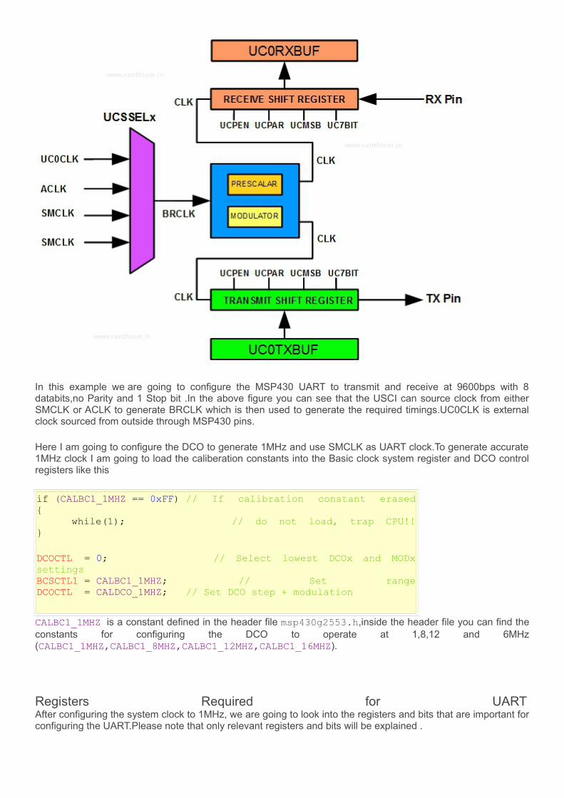
In this article we we will configure USCI_A0 in MSP430G2553 to handle asynchronous serial communication or commonly known as UART mode.The UART mode uses two pins to transmit(UCA0TXD) and receive data(UCA0RXD) .Asynchronous serial communication is widely used for communicating with external devices like PC/Laptops,GSM modems,GPS modules etc.It also forms the basis for many standard protocols like RS232,RS422,RS485 etc.
You can see the (very) simplified block diagram of USCI_A0 in UART mode below.
In this example we are going to configure the MSP430 UART to transmit and receive at 9600bps with 8 databits,no Parity and 1 Stop bit .In the above figure you can see that the USCI can source clock from either SMCLK or ACLK to generate BRCLK which is then used to generate the required timings.UC0CLK is external clock sourced from outside through MSP430 pins.
Here I am going to configure the DCO to generate 1MHz and use SMCLK as UART clock.To generate accurate 1MHz clock I am going to load the caliberation constants into the Basic clock system register and DCO control registers like this
if (CALBC1_1MHZ == 0xFF) // If calibration constant erased{ while(1); // do not load, trap CPU!!}
DCOCTL = 0; // Select lowest DCOx and MODx settingsBCSCTL1 = CALBC1_1MHZ; // Set rangeDCOCTL = CALDCO_1MHZ; // Set DCO step + modulation
CALBC1_1MHZ is a constant defined in the header file msp430g2553.h,inside the header file you can find the constants for configuring the DCO to operate at 1,8,12 and 6MHz (CALBC1_1MHZ,CALBC1_8MHZ,CALBC1_12MHZ,CALBC1_16MHZ).
Registers Required for UART After configuring the system clock to 1MHz, we are going to look into the registers and bits that are important for configuring the UART.Please note that only relevant registers and bits will be explained .
1) UCAxCTL0 (USCI_Ax Control register0) here we are dealing with USC1_A0 so UCA0CTL0 -This register controls the settings for Parity selection,direction of data transmission(LSB or MSB first),character length,no of stop bits,modes of serial transmission.
The important bits are
UCPEN Used for enabling or disabling parity (In our case no parity so UCPEN = 0)
UCPAR Used for selecting between EVEN or ODD parity (not used since we are disabling parity)
UCMSB Controls the direction of receive and transmit shift register(here LSB first)
UC7BIT Selects the character length 7/8 bit(we are using 8 bit so 0)
UCSPB Number of stopbits (here 1 so UCSPB = 0)
UCMODEx2 bits used to select the asynchronous mode when UCSYNC = 0.Here we areusing the default UART mode.Other modes are used with multiprocessor serial communication and for automatic baudrate detection
UCSYNC Selecting between asynchronous(UART) and synchronous modes(SPI)
In our case ,all the bits in UCA0CTL0 are zero so we won't be configuring that register in our program.
2) UCAxCTL1 here UCA0CTL1-The two important bits contained in this register are
UCSSELxThese bits are used to select the clock source to the USCI module.In our case we are going to select SMCLK @1MHz.
UCSWRSTThis bit is used to put the USCI module in reset state .It is recommended to put the USCI module in reset state before making any changes to the registers.
3) UCAxSTAT here UCA0STAT-The two important bits contained in this register are
UCLISTENThis bit is used to select the internal loop back mode.In loop back mode UCAxTXD is internally fed back to the receiver.
UCBUSY Indicates if a transmit or receive operation is in progress.
4) UCAxBR0 (UCA0BR0) and UCAxBR1 (UCA0BR1) are two 8 bit registers which are used to set the clock prescalar value for the Baud rate generator.
5) UCAxTXBUF (UCA0TXBUF) 8 bit data register for holding the byte to be transmitted by the MSP430 UART.
6) UCAxRXBUF (UCA0RXBUF) 8 bit data register that stores the received byte.
Configuring the Baud rate MSP430 data sheet has an indepth description about configuring the baud rate for various modes.Easiest way to configure the baud rate of a MSP430 device is to use the Baud rate selection table listed in the usermanual.Just find out the UCBRx values corrosponding to your BRCLK frequency and the baud rate you wish to use .After finding out values just put them in the UCA0BR0 and UCA0BR1 register to configure the baud rate.
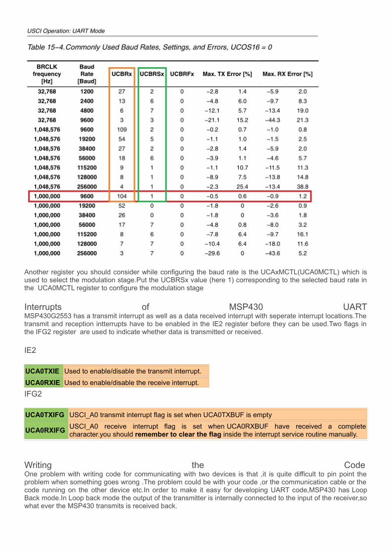
In our case we are using SMCLK @ 1MHz as BRCLK and 9600bps as the baud rate .Now check the table for the corresponding UCBRx value (here 104) and put them in UCA0BR0 and UCA0BR1 registers to configure the baud rate.You can find the below table in the MSP430x2xxx usermanual.
Another register you should consider while configuring the baud rate is the UCAxMCTL(UCA0MCTL) which is used to select the modulation stage.Put the UCBRSx value (here 1) corresponding to the selected baud rate in the UCA0MCTL register to configure the modulation stage
Interrupts of MSP430 UARTMSP430G2553 has a transmit interrupt as well as a data received interrupt with seperate interrupt locations.The transmit and reception intterrupts have to be enabled in the IE2 register before they can be used.Two flags in the IFG2 register are used to indicate whether data is transmitted or received.
IE2
UCA0TXIE Used to enable/disable the transmit interrupt.
UCA0RXIE Used to enable/disable the receive interrupt.
IFG2
UCA0TXIFG USCI_A0 transmit interrupt flag is set when UCA0TXBUF is empty
UCA0RXIFGUSCI_A0 receive interrupt flag is set when UCA0RXBUF have received a complete character.you should remember to clear the flag inside the interrupt service routine manually.
Writing the Code One problem with writing code for communicating with two devices is that ,it is quite difficult to pin point the problem when something goes wrong .The problem could be with your code ,or the communication cable or the code running on the other device etc.In order to make it easy for developing UART code,MSP430 has Loop Back mode.In Loop back mode the output of the transmitter is internally connected to the input of the receiver,so what ever the MSP430 transmits is received back.
In this example we are going to write simple communication program which uses the loop back mode and communicates at 9600bps (8N1).Here I am using IAR embedded workbench for MSP430 from IAR.If you are not familiar with IAR EW you can check out a short tutorial here .
The code given below will configure the UART and transmit an ascii character 'A' .The UART is configured in loop back mode so 'A' is received back and is stored in UCA0RXBUF.LED connected to P1.0 is lighted when 'A' is transmitted and LED connected to P1.6 is lighted when 'A' is received back.
#include "msp430g2553.h"void main(void){ WDTCTL = WDTPW + WDTHOLD; // Stop the Watch dog //------------------- Configure the Clocks -------------------// if (CALBC1_1MHZ==0xFF) // If calibration constant erased { while(1); // do not load, trap CPU!! }
DCOCTL = 0; // Select lowest DCOx and MODx settings BCSCTL1 = CALBC1_1MHZ; // Set range DCOCTL = CALDCO_1MHZ; // Set DCO step + modulation //---------------- Configuring the LED's ----------------------// P1DIR |= BIT0 + BIT6; // P1.0 and P1.6 output P1OUT &= ~BIT0 + BIT6; // P1.0 and P1.6 = 0 //--------- Setting the UART function for P1.1 & P1.2 --------// P1SEL |= BIT1 + BIT2; // P1.1 UCA0RXD input P1SEL2 |= BIT1 + BIT2; // P1.2 UCA0TXD output //------------ Configuring the UART(USCI_A0) ----------------// UCA0CTL1 |= UCSSEL_2 + UCSWRST; // USCI Clock = SMCLK,USCI_A0 disabled UCA0BR0 = 104; // 104 From datasheet table- UCA0BR1 = 0; // -selects baudrate =9600,clk = SMCLK UCA0MCTL = UCBRS_1; // Modulation value = 1 from datasheet UCA0STAT |= UCLISTEN; // loop back mode enabled UCA0CTL1 &= ~UCSWRST; // Clear UCSWRST to enable USCI_A0 //---------------- Enabling the interrupts ------------------// IE2 |= UCA0TXIE; // Enable the Transmit interrupt IE2 |= UCA0RXIE; // Enable the Receive interrupt _BIS_SR(GIE); // Enable the global interrupt UCA0TXBUF = 'A'; // Transmit a byte _BIS_SR(LPM0_bits + GIE); // Going to LPM0}
//-----------------------------------------------------------------------// // Transmit and Receive interrupts // //-----------------------------------------------------------------------//
#pragma vector = USCIAB0RX_VECTOR __interrupt void ReceiveInterrupt(void) { P1OUT ^= BIT6; // light up P1.6 LED on RX IFG2 &= ~UCA0RXIFG; // Clear RX flag }
After the WDT is stopped .The DCO is configured to produce clock at 1MHz using the calliberation constants.The ports P1.0 and P1.6 are configured as outputs to light up the respective LED' during transmission and reception.
In MSP430G2553, P1.1 and P1.2 are configured as UCA0RXD and UCA0TXD using their respective PXSEL registers.The clock for USCI_A0 in UART mode is sourced from SMCLK and other parameters are configured.
The UART module is configured to act in loop back mode using UCA0STAT |= UCLISTEN;
Here I am using both transmit and receive interrupts which are enabled in IE2 .GIE bit is also enabled.
UART transmits a character 'A' by writing it into UCA0TXBUF.After the character is transmitted,Transmit interrupt is generated which lights up the P1.0 LED.
The character is received back UCA0RXBUF and a recceive interrupt is generated which lights up the P1.6 LED.
You should remember to clear the UCA0RXIFG flag inside the ISR manually.
After you have successfully run the above program in Launchpad you can remove the loop back mode by commenting out UCA0STAT |= UCLISTEN; .After that line is removed, RXD and TXD pins are now routed to P1.1 and P1.2.You can connect P1.1 and P1.2 and run the program,the two LED connected to P1.0 and P1.6 should light up.
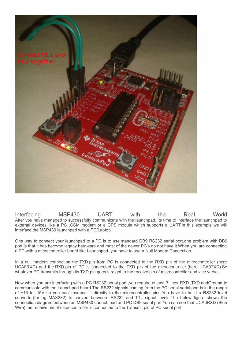
Interfacing MSP430 UART with the Real WorldAfter you have managed to successfully communicate with the launchpad, its time to interface the launchpad to external devices like a PC ,GSM modem or a GPS module which supports a UART.In this example we will interface the MSP430 launchpad with a PC/Laptop.
One way to connect your launchpad to a PC is to use standard DB9 RS232 serial port,one problem with DB9 port is that it has become legacy hardware and most of the newer PC's do not have it.When you are connecting a PC with a microcontroller board like Launchpad ,you have to use a Null Modem Connection.
In a null modem connection the TXD pin from PC is connected to the RXD pin of the microcontroller (here UCA0RXD) and the RXD pin of PC is connected to the TXD pin of the microcontroller (here UCA0TXD).So whatever PC transmits through its TXD pin goes straight to the receive pin of microcontroller and vice versa.
Now when you are interfacing with a PC RS232 serial port ,you require atleast 3 lines RXD ,TXD andGround to communicate with the Launchpad board.The RS232 signals coming from the PC serial serial port is in the range of +15 to -15V so you can't connect it directly to the microcontroller pins.You have to build a RS232 level converter(for eg MAX232) to convert between RS232 and TTL signal levels.The below figure shows the connection diagram between an MSP430 Launch pad and PC DB9 serial port.You can see that UCA0RXD (Blue Wire) the receive pin of microcontroller is connected to the Transmit pin of PC serial port.
As I have already mentioned DB9 ports are being replaced with USB ports in most PC's and Laptops,So another way to interface the Launchpad with PC is by using an USB to Serial converter board.USB to Serial Converter boards provide a virtual serial port which you can read and write like a standard serial port.When you read or write to the virtual serial port,the data you send is then passed theough the standard USB port to the Converter chip (eg FT232) which translates to serial data stream.
Her I am using USB2SERIAL USB to Serial/RS232/RS485 converter to interface the launchpad with my Laptop.The TTL outputs of TX and RX pins of FT232 are available outside which are then connected to UCA0RXD and UCA0TXD pins of MSP430G2553 respectivly as shown in the below table .USB2SERIAL boards has 3.3V /5V signal level select which makes it safe to interface directly with MSP430 (3.3V logic) pins.
While communicating,you should have some sort of terminal program like PuTTY (on PC) for listening in on the bytes send by the launchpad board.Open "Device Manager" on Windows to find out the COM port number of your virtual serial port and configure PuTTY to communicate with that port.If you are interested in setting up serial connection with other Operating systems like Linux , you can check out my serial communication tutorials.PuTTY is availablle for Linux also.
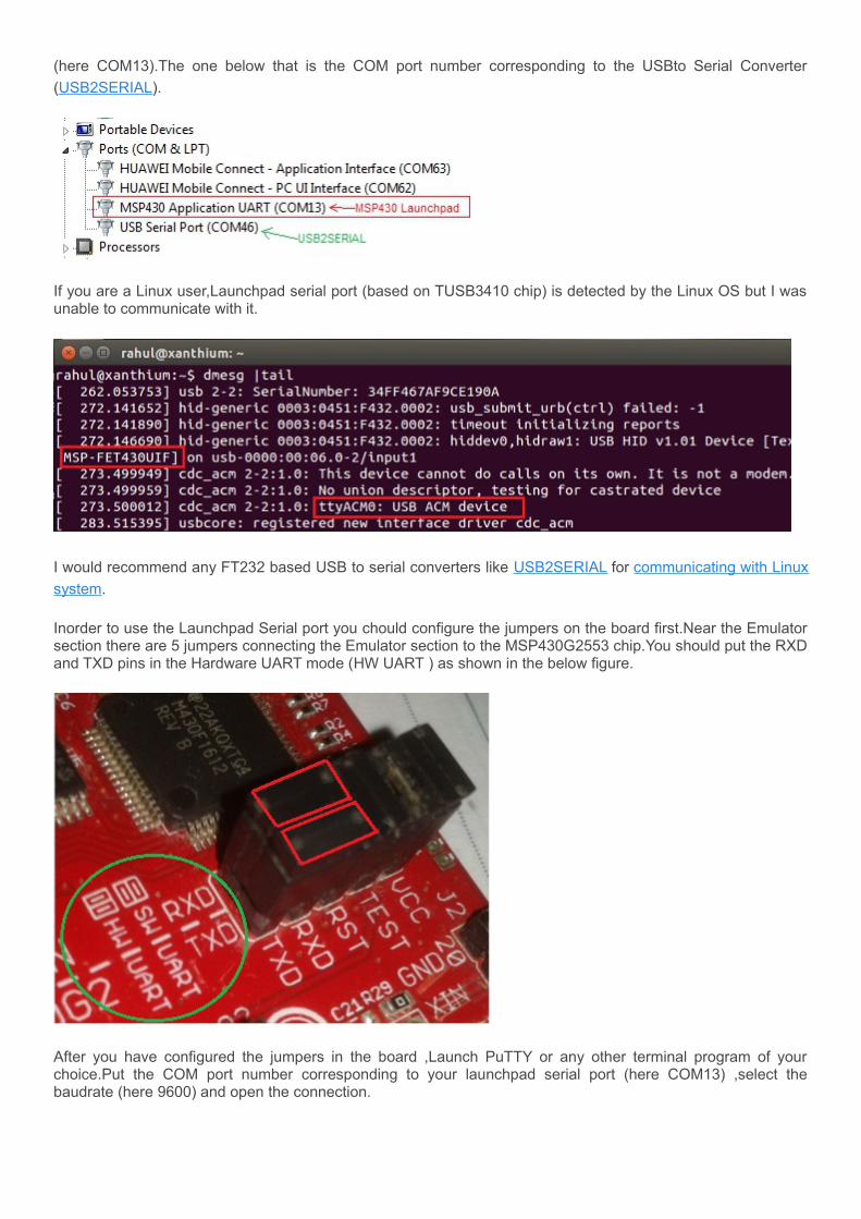
Using MSP430 Launchpad Serial Port In Launchpad, the TUSB3410 chip( inside the emulator section) can act as a USB to Serial converter too.If you
check under "Device Manager" you can see that as "MSP430 Application UART COMxx",highlighted in red
(here COM13).The one below that is the COM port number corresponding to the USBto Serial Converter
(USB2SERIAL).
If you are a Linux user,Launchpad serial port (based on TUSB3410 chip) is detected by the Linux OS but I was unable to communicate with it.
I would recommend any FT232 based USB to serial converters like USB2SERIAL for communicating with Linux
system.
Inorder to use the Launchpad Serial port you chould configure the jumpers on the board first.Near the Emulator section there are 5 jumpers connecting the Emulator section to the MSP430G2553 chip.You should put the RXD and TXD pins in the Hardware UART mode (HW UART ) as shown in the below figure.
After you have configured the jumpers in the board ,Launch PuTTY or any other terminal program of your choice.Put the COM port number corresponding to your launchpad serial port (here COM13) ,select the baudrate (here 9600) and open the connection.
Now download the program we discussed above and reset the board.The MSP430 will transmit a character 'A" which will be dispalyed on the PuTTY terminal as shown in the figure below.(I have reseted the board a few times). If you press any key on the keyboard,it will be transmitted to the MSP430 board and the LED connected to P1.6 will toggle.
So there its is communicating between a PC and a Launchpad development board.
One problem with serial communication format like RS232 and USB is there limited range,these standards are not suitable for transmitting data over several 100's of meters.If you want to transmit data over long distances using twisted pair cables you have to use RS485 protocol.
If you are interested you can check our next section where we are going to interface a MAX485 chip with the Launchpad board.