FACTA UNIVERSITATIS Series: Automatic Control and Robotics Vol. 11, N o 1, 2012, pp. 1 - 14 POSITION RESOLVED MULTI CHANNEL TRANSIENT CURRENT TECHNIQUE UDC 539.1.074 666.952 681.138.8 Marko Milovanović 1 , Gregor Kramberger 1 , Igor Mandić 1 , Vladimir Cindro 1 , Marko Mikuž 1,2 , Marko Zavrtanik 1 , Graeme Stewart 3 1 Jožef Stefan Institute, Ljubljana, Slovenia 2 University of Ljubljana, Faculty of Mathematics and Physics, Ljubljana, Slovenia 3 University of Glasgow, School of Physics and Astronomy, Kelvin Building, Glasgow, UK Abstract. With perpetual need for examining new sensor structures for dosimetry, calorimetry and particle tracking experiments, many techniques were developed during the last couple of decades, which make studies of both microscopic and macroscopic detector properties possible. The conventional Transient Current Technique is a key tool for studying signal formation, charge collection and trapping mechanisms inside the semiconductor detector. However, studies of segmented devices require very good position resolution of deposited charge for examining the position resolved charge collection properties in such detectors. To meet all this demands, a position sensitive multi channel TCT setup was made which utilizes an IR laser with very small FWHM (~7 μm), while also providing submicron movement precision with a large scanning range. This technique offers examining of complex structures, involving all types of position sensitive silicon detectors (pad, strip, pixel, 3D), as well as MOS structures (RADFETs, capacitors, etc.). Some of the experimental results will be presented in this paper, merely as examples of this technique’s potential. Key words: silicon particle detectors, radiation damage, dosimeters 1. INTRODUCTION In an effort to understand the underlying physics behind every semiconductor detector device used for particle tracking, timing applications or dosimetry, many different ap- proaches and techniques have arisen during the course of their ever increasing usage. The semiconductor detectors mostly used for these studies are basically solid state ionization chambers, which can be achieved by means of a reverse polarized p-n junction, a Schot- tky barrier, or even two ohmic contacts for large band gap semiconductors. The passage Received June 4, 2012 Corresponding author: Marko Milovanović Jožef Stefan Institute, Jamova 39, SI-1000 Ljubljana, Slovenia • E-mail: [email protected]
Transcript
FACTA UNIVERSITATIS Series: Automatic Control and Robotics Vol. 11, No 1, 2012, pp. 1 - 14
POSITION RESOLVED MULTI CHANNEL TRANSIENT CURRENT TECHNIQUE
UDC 539.1.074 666.952 681.138.8
Marko Milovanović1, Gregor Kramberger1, Igor Mandić1, Vladimir Cindro1, Marko Mikuž1,2, Marko Zavrtanik1, Graeme Stewart3
1Jožef Stefan Institute, Ljubljana, Slovenia 2University of Ljubljana, Faculty of Mathematics and Physics, Ljubljana, Slovenia
3University of Glasgow, School of Physics and Astronomy, Kelvin Building, Glasgow, UK
Abstract. With perpetual need for examining new sensor structures for dosimetry, calorimetry and particle tracking experiments, many techniques were developed during the last couple of decades, which make studies of both microscopic and macroscopic detector properties possible. The conventional Transient Current Technique is a key tool for studying signal formation, charge collection and trapping mechanisms inside the semiconductor detector. However, studies of segmented devices require very good position resolution of deposited charge for examining the position resolved charge collection properties in such detectors. To meet all this demands, a position sensitive multi channel TCT setup was made which utilizes an IR laser with very small FWHM (~7 μm), while also providing submicron movement precision with a large scanning range. This technique offers examining of complex structures, involving all types of position sensitive silicon detectors (pad, strip, pixel, 3D), as well as MOS structures (RADFETs, capacitors, etc.). Some of the experimental results will be presented in this paper, merely as examples of this technique’s potential.
In an effort to understand the underlying physics behind every semiconductor detector device used for particle tracking, timing applications or dosimetry, many different ap-proaches and techniques have arisen during the course of their ever increasing usage. The semiconductor detectors mostly used for these studies are basically solid state ionization chambers, which can be achieved by means of a reverse polarized p-n junction, a Schot-tky barrier, or even two ohmic contacts for large band gap semiconductors. The passage
Received June 4, 2012 Corresponding author: Marko Milovanović Jožef Stefan Institute, Jamova 39, SI-1000 Ljubljana, Slovenia • E-mail: [email protected]
2 M. MILOVANOVIĆ, G. KRAMBERGER, I. MANDIĆ et al.
of ionizing radiation creates electron-hole pairs which then drift in an electric field, thus inducing measurable current in the external electrical circuit. In energy measurements, accomplished by calorimeter detectors, the particle is stopped inside the detector so that the signal is proportional to its energy. In high energy tracking experiments, the particle traverses a detector with finely segmented electrodes (strip or pixel detectors), yielding high position resolution information (from around micron to a few tens of microns). Mul-tiple layers of detectors make track reconstruction possible, which can be used for mo-mentum and charge analysis of the traversing particle. In addition, to meet higher colli-sion rates and thus higher radiation damage in future HEP experiments, like the ones at the foreseen High Luminosity Large Hadron Collider (HL-LHC) [1] at CERN, new de-tector device structures were developed to withstand such harsh operating condition. One of the proposed devices is a 3D detector [2]. This device has doped collection electrodes penetrating almost throughout the entire substrate, therefore providing short collection times, low depletion voltages and higher radiation tolerance.
Semiconductor sensors are also widely used for measuring the exposure to ionizing radiation. They have many advantages in terms of power requirements and their sizes over conventional detectors. Among such sensors, a metal oxide field effect transistor (MOSFET) is becoming increasingly popular. When properly designed, such p-channel structure is a Radiation-Sensing-Field-Effect-Transistor (RADFET). It is an integrating dosimeter that measures the dose (rad or Gy(Si)) by virtue of the change in voltage needed for allowing current to flow in p-MOS transistors. The change is due to a positive oxide charge accumulated in the silicon oxide (SiO2) by irradiation. It has application in aerospace industry, medicine, nuclear industry and science.
To examine the performance of these structures and determine how different geome-tries, radiation damage, temperature, annealing affects their operation and efficiency, one turns to different measurement/probing techniques. Measurements of the capacitance-voltage (CV) and current-voltage (IV) characteristics of the samples obtain macroscopic detector parameters – e.g. for silicon detectors based on p-n junction: full depletion volt-age (Vfd)
1 and leakage current (Ileak). To study signal formation, charge collection and trapping mechanisms2 inside the detector, a Transient Current Technique (TCT) is com-monly used. The basic principle of this technique is to generate free charge carriers inside the detector device by a short laser pulse or an incident particle and observe the induced current waveform that arises from their drift.
By utilizing this technique with additional sub-micron precision translator stages, a full 3D position sensitive system can be achieved which can be used to examine structures with very high position resolution (~7 μm). In this paper, some of the above mentioned semiconductor structures were examined in different ways and a few examples of possible usage will be presented.
1 The voltage necessary to create high enough electric field in a reversely biased detector to deplete the full thickness of the detector of free charge carriers, thus obtaining acceptable SNR. 2 Parts of the charge carriers during their drift can be trapped by crystallographic defects in the silicon bulk (called also the trapping centers), which occur and gradually increase with strong irradiation. Trapping of signal charge carriers leads to degradation in charge collection efficiency.
Position Resolved Multi Channel Transient Current Technique 3
2. EXPERIMENTAL SETUP, TECHNIQUE AND DEVICES
A schematic view of the experimental setup at Jožef Stefan Institute in Ljubljana is shown in Fig. 1.
Fig. 1. Schematic view of the experimental setup
The samples are mounted on a thermally controlled support (copper or/and alumi-num), which can be stabilized using a Peltier thermoelectric cooler in temperature range from -20 ºC to 60ºC. The connection to a high voltage power supply was made via bias tee, which is used to decouple the readout electronics from high DC bias voltage. The signal from the device under study is amplified by a wide band amplifier and digitized by a 1 GHz oscilloscope. The signal was averaged over many (a few hundred) laser pulse repetitions at each space point. A track of electron-hole pairs simulating minimum ioniz-ing particle (MIP) is created by use of infra-red laser (λ = 1064 nm) with a pulse width of 40 ps and repetition rate of up to 1 MHz. A focusing system ensures the beam diameter of ~7 μm (FWHM) to be found at its waist. For certain devices and application, red laser (λ = 670 nm) may also be used instead and one would expect a factor 2 better achievable FWHM. The position of the beam is controlled by three orthogonal moving stages with a sub-micron resolution, forming a full 3D translation system. The picture of the actual setup, without the attached instruments, is shown in Fig. 2.
4 M. MILOVANOVIĆ, G. KRAMBERGER, I. MANDIĆ et al.
Fig. 2. The picture of the actual setup (without the attached instruments)
The software for remote controlling the moving stages, high voltage supply and ac-quiring the waveforms from the oscilloscope was developed using LabVIEW platform. The connection to the devices was made by using the IEEE-488 interface bus (GPIB). The user interface (front panel) is shown in Fig. 3.
Fig. 3. Software user interface
Position Resolved Multi Channel Transient Current Technique 5
The basic principle of the technique is to generate charge inside any device under study and measure the induced (transient) current. Further analysis of this current offers many parameters to be extracted (e.g. Vfd, Effective trapping time3, velocity of generated charge carriers, etc.). The magnitude of the induced current Ie,h at a certain time t after generation is given by Eq.1:
, ,/0, , ,( ) ( )eff e ht
e h e h e h
A qI t N e v t
W
(1)
where A is the amplifier gain, q0 is the elementary charge and Ne,h is the number of gener-ated e-h pairs. The term 1/W determines the weighting field4 inside the detector (simple pad geometry assumed), where W is the detector thickness, τeff,e,h are effective trapping times of electrons and holes and ve,h(t) their drift velocities.
This means that at a given beam position, by using Eq.1 the induced current in the detector can be calculated as the sum of electron and hole contribution to the signal. Therefore the electric field (determined by the relation ve,h = μe,h·E, where μe,h is electron or hole mobility) and trapping parameters can be extracted from the time evolution of the pulse. However, with severe trapping at high fluences, this is rather difficult because the signal vanishes exponentially with time.
There are various TCT methods which can investigate different aspects of charge col-lection and they mainly differ in the location or depth where the original charge is created inside the sample. In our study, the described setup can be used in two different ways (Fig. 4):
1) Standard (top) TCT – where the device is illuminated and examined from the top (either front or rear electrode). The depth of e-h pair generation depends on the wavelength of the light or energy and type of ionizing particle and of course on the semiconductor. In silicon for example, λ = 670 nm penetrates only a few microns, similarly alpha particles penetrate around 20 μm, while IR (1064 nm) penetrates a few millimeters, which is similar to the ionizing electrons from a radioactive source (e.g. 90Sr).
2) Edge-TCT – where the device is illuminated from the side by an IR laser, in which case the e-h pairs are created at a certain depth inside the structure. By using Eq.1 and looking at current amplitude immediately after injection (t ~ 0), the trapping
becomes insignificant ( 1,,/ heeffte ) and therefore the signal is proportional to drift velocity of the carriers at given position. Therefore, the term E(y) = vdr,e,h(y)/μe,h can be determined without detailed information on induced current pulse evolution with time and thereby making possible to extract the velocity and electric field pro-files inside the detector [6-8].
3 Trapping centers seize electrons from the conduction band or holes from the valence band and re-emit them back after some time [3, 4] 4 Depends on the coupling between the charge and the individual electrodes [5].
6 M. MILOVANOVIĆ, G. KRAMBERGER, I. MANDIĆ et al.
Fig. 4. Basic principle of TCT (a sample detector structure)
Devices under study may be all types of silicon detector structures (position sensitive silicon detectors, CCD, MOSFET structures/RADFET, pin diodes, etc.). Due to severe radiation effects it is particularly challenging to measure irradiated silicon devices. In order to perform these studies, the samples were irradiated with neutrons at the TRIGA nuclear reactor facility of Jožef Stefan Institute in Ljubljana [9]. Since the temperature stabilization of the sample has a very wide range, it allowed also for controlled annealing inside the setup. Studies on three different structures, planar strip detectors, 3D detectors, and RADFETs will be presented in this paper.
3. RESULTS
3.1. Strip detector
One of the strip detectors that will be used for demonstrating the edge-TCT. The photo of the device is given in Fig. 5a, as well as a schematic view of a general strip de-tector device (Fig. 5b). The detector is 1.25 x 1.25 cm2 in size, fabricated on ~300 μm thick p-type substrate. The strips are 1 cm long, n-type implanted ~20 μm in width and AC coupled, with a pitch of 100 μm. Full depletion voltage was found to be around 16 V.
Fig. 5. A photo of the device under study with a zoomed segment at the edge
1.25 cm
Strip pitch: ~75 μm
Bias ring
Guard rings
Readout strips (with bonding pads)
Poly-silicon
resistors
Standard-TCT (charged particle or IR/Red laser)
front electrode
Edge-TCT (IR laser)
p-type silicon bulk
front-end electronics x
y
W
p+ implant
n+ implant
rear electrode
oxide (SiO2)
holes
electrons
Position Resolved Multi Channel Transient Current Technique 7
Fig. 6a shows the induced current pulses (Eq.1) for different injection depths y in the detector. The contribution to the signal of both electrons and holes generated at each depth can be clearly distinguished [6]. At low y (close to the strips) the peak at the signal beginning is developed from superposition of electron and hole drift currents in the high electric field region. The long tail of the signal comes from the drift of the holes towards the region of low electric field (backplane). As the beam moves towards the backplane (greater y), this tail becomes shorter, due to shorter hole drift distance, and at the same time, the peak coming from the electrons, becomes wider, due to longer drift path of electrons. Since the Vfd is around 16 V, it is also obvious that the whole volume of the detector is active. If the bias voltage is increased (Fig. 6b), it reduces the width of the pulse and increases the amplitude.
(a) (b)
Fig. 6. Induced current pulse shapes in a non-irradiated detector at T = 20 ºC for: (a) different depths at Vbias = 100 V, (b) different bias voltages at y = 30 μm.
One of the main purposes of this technique was to study the radiation damage in sili-con detectors installed in large scale experiments at the LHC. During the expected life-time of the detectors, they will be traversed by a large amount of particles which will sub-stantially distort the lattice of the crystal and hence introduce energy levels – traps, in the band gap. After the envisaged lifetime of the experiment (~ 5·1014 particles/cm-2) the de-vice properties will change mainly in three ways: leakage current increase, very high de-pletion voltage and trapping of the drifting charge (whereas only the latter two will influ-ence the signal). As one can see in Fig. 7a, with the detector irradiated with neutrons to that equivalent fluence, 500 V is not enough to fully deplete the sensor as concluded from the fact that there is almost no signal from y = 220 μm. One can also observe that the sig-nal is short which would not be the case without the trapping. An interesting observation is also the "double junction" which can be noticed at y = 270 μm [10, 11]. Although the electric field at the back is much weaker than for the main junction at the strips. The higher voltage for irradiated detector (Fig. 7b) increases the signal in both amplitude and width, due to growth of the depleted region.
electron signal
hole signal
8 M. MILOVANOVIĆ, G. KRAMBERGER, I. MANDIĆ et al.
(a) (b)
Fig. 7. Induced current pulses in a detector irradiated to 214105 cmeq at T = -20 ºC for:
(a) different depths at Vbias = 500 V, (b) different bias voltages at y = 30 μm.
However, even more interesting is the situation if the detectors are traversed by even larger amount of particles after the LHC upgrade (~ 5·1015 particles/cm-2). By integrating the current pulses generated at every injection depth, collected charge can be observed as a function of detector depth and Fig. 8a shows the charge collection profiles for the same detector irradiated to this equivalent fluence. Here one can see that unlike expectations, the signal is obtained from all detector depths, indicating a new device model is required in understanding n+-p junction after heavy irradiation. The drift velocity profile in Fig. 8b proves this even more so.
(a) (b)
Fig. 8. Charge collection (a) and drift velocity (b) profiles for a detector irradiated to 215105 cmeq.
Annealing studies were performed on the same detector after irradiation to this flu-ence, and a very strong influence of charge multiplication due to impact ionization in high electric fields was observed after longer annealing times. This process generally leads to higher amount of detected charge. The reason can be in a very simplistic way explained by an increase of amount of negative space charge (acceptors) and consequently peak electric field in the detector with annealing [12, 13]. This is very well observed in the induced current pulses.
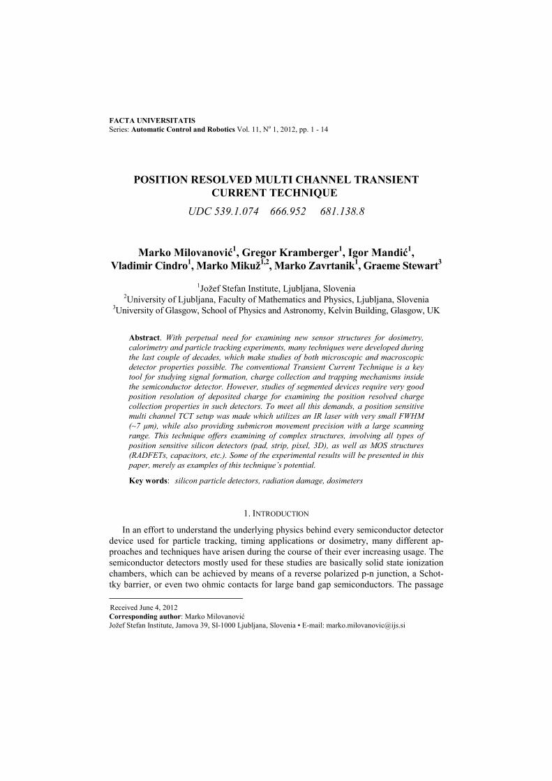
Fig. 9a and 9b show how the waveforms change for different injection depths (50 μm and 150 μm) after several cumulative annealing stages at 60ºC, and Fig. 9c and 9d at dif-
Position Resolved Multi Channel Transient Current Technique 9
ferent bias voltages after 640 min of annealing. At longer annealing times, it is clear that voltages above Vbias ≥ 500 V are sufficient to cause a second peak in the signal to appear for any injection depth. This peak originates from electrons undergoing multiplication in the high electric field region close to the strips [8]. It even becomes the dominant one after a certain annealing time, and it is clearly separated from the first peak at 150 μm. The first peak, originated from the primarily generated carriers, is seen to remain similar at all annealing stages.
(a) (b)
(c) (d)
Fig. 9. (a) Induced current pulses at 700 V for different annealing times at injection depth of 50 μm and (b) 150 μm. (c) – Induced current pulses at different bias voltages after 640 min of annealing at 60 ºC for injection depth of 50 μm and (d) 150 μm.
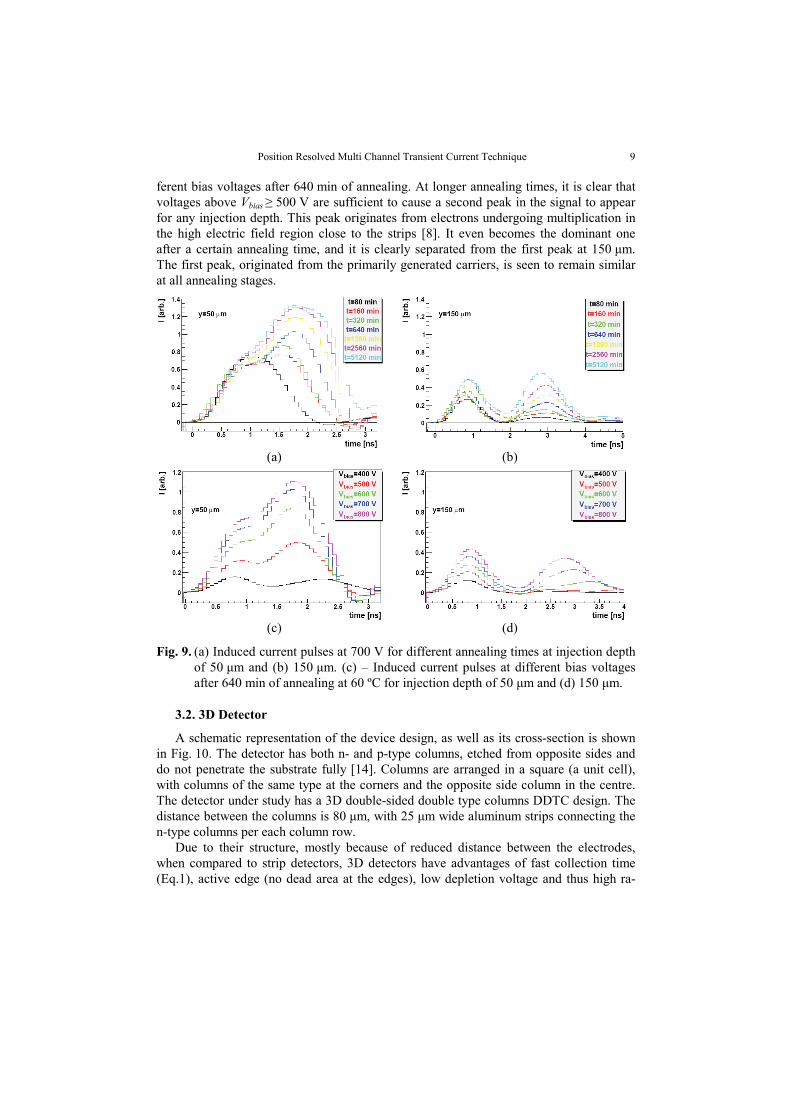
3.2. 3D Detector
A schematic representation of the device design, as well as its cross-section is shown in Fig. 10. The detector has both n- and p-type columns, etched from opposite sides and do not penetrate the substrate fully [14]. Columns are arranged in a square (a unit cell), with columns of the same type at the corners and the opposite side column in the centre. The detector under study has a 3D double-sided double type columns DDTC design. The distance between the columns is 80 μm, with 25 μm wide aluminum strips connecting the n-type columns per each column row.
Due to their structure, mostly because of reduced distance between the electrodes, when compared to strip detectors, 3D detectors have advantages of fast collection time (Eq.1), active edge (no dead area at the edges), low depletion voltage and thus high ra-
10 M. MILOVANOVIĆ, G. KRAMBERGER, I. MANDIĆ et al.
diation hardness. Their disadvantages in general include complex processing, larger noise due to higher capacitance and the existence of regions with relatively low electric field.
(a) (b)
Fig. 10. Design and a cross section of a 3D DDTC detector by CNM, Barcelona.
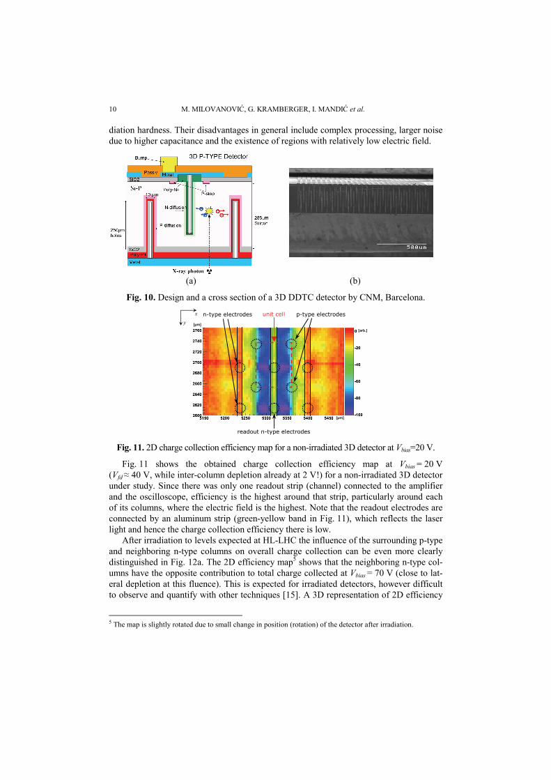
Fig. 11. 2D charge collection efficiency map for a non-irradiated 3D detector at Vbias=20 V.
Fig. 11 shows the obtained charge collection efficiency map at Vbias = 20 V (Vfd ≈ 40 V, while inter-column depletion already at 2 V!) for a non-irradiated 3D detector under study. Since there was only one readout strip (channel) connected to the amplifier and the oscilloscope, efficiency is the highest around that strip, particularly around each of its columns, where the electric field is the highest. Note that the readout electrodes are connected by an aluminum strip (green-yellow band in Fig. 11), which reflects the laser light and hence the charge collection efficiency there is low.
After irradiation to levels expected at HL-LHC the influence of the surrounding p-type and neighboring n-type columns on overall charge collection can be even more clearly distinguished in Fig. 12a. The 2D efficiency map5 shows that the neighboring n-type col-umns have the opposite contribution to total charge collected at Vbias = 70 V (close to lat-eral depletion at this fluence). This is expected for irradiated detectors, however difficult to observe and quantify with other techniques [15]. A 3D representation of 2D efficiency
5 The map is slightly rotated due to small change in position (rotation) of the detector after irradiation.
n-type electrodes p-type electrodes
readout n-type electrodes
unit cell y
x
[μm]
[μm]
[arb.]
Position Resolved Multi Channel Transient Current Technique 11
map using z-axis instead of color encoding in Fig. 12b shows charge collection efficiency at the highest measured bias voltage, Vbias = 400 V.
(a) (b)
Fig. 12. (a) 2D efficiency map at Vbias= 70 V and (b) its 3D representation at Vbias= 400 V of the detector surface (top) irradiated to Φeq= 5·1015 cm-2.
If the laser scans are made across the edge of the detector (edge-TCT), the charge collection efficiency can be observed per each column length unit. Fig. 13 shows 2D effi-ciency maps for a non-irradiated detector, biased at Vbias = 20 V.
(a) (b)
Fig. 13. (a) 2D efficiency map and (b) its 3D representation of a non-irradiated detector edge at Vbias = 20 V.
The map shows slightly smeared in vertical direction due to large distance between the bonded strip and detector edge (~3 mm). The laser beam has a Gaussian profile, therefore is much wider at the edge of the detector than at the waist and consequently injects small amounts of charge.
3.3. RADFET
RADiation-sensing Field-Effect Transistor is a miniature type of integrating radiation dosimeter, which is based on a metal-oxide silicon p-channel structure. It measures the dose as the field changes when positive charge caused by ionizing radiation is trapped in the silicon oxide (Si02). An electrical measurement (shift or threshold voltage) then gives a relative value of the dose.
y
xQ
x
y
[μm]
[μm]
[arb.]
n-type electrodes
p-type electrodes
Q
x y
y
x[μm]
[μm]
[arb.]
12 M. MILOVANOVIĆ, G. KRAMBERGER, I. MANDIĆ et al.
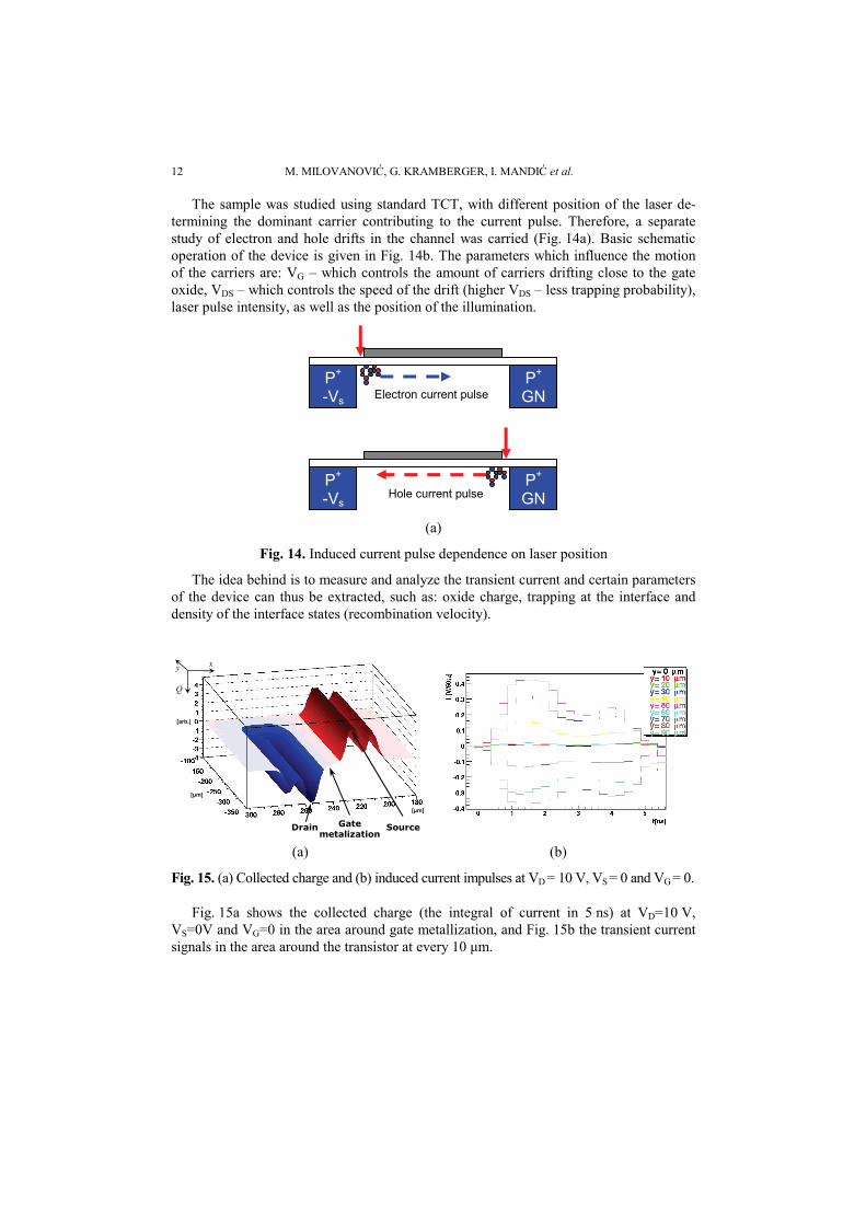
The sample was studied using standard TCT, with different position of the laser de-termining the dominant carrier contributing to the current pulse. Therefore, a separate study of electron and hole drifts in the channel was carried (Fig. 14a). Basic schematic operation of the device is given in Fig. 14b. The parameters which influence the motion of the carriers are: VG – which controls the amount of carriers drifting close to the gate oxide, VDS – which controls the speed of the drift (higher VDS – less trapping probability), laser pulse intensity, as well as the position of the illumination.
(a)
Fig. 14. Induced current pulse dependence on laser position
The idea behind is to measure and analyze the transient current and certain parameters of the device can thus be extracted, such as: oxide charge, trapping at the interface and density of the interface states (recombination velocity).
(a) (b)
Fig. 15. (a) Collected charge and (b) induced current impulses at VD = 10 V, VS = 0 and VG = 0.
Fig. 15a shows the collected charge (the integral of current in 5 ns) at VD=10 V, VS=0V and VG=0 in the area around gate metallization, and Fig. 15b the transient current signals in the area around the transistor at every 10 μm.
P+ GN
P+ -Vs
P+ GN
P+ -Vs
Hole current pulse
Electron current pulse
Gate metalization
Source Drain
Q
x y
[μm]
[μm]
[arb.]
Position Resolved Multi Channel Transient Current Technique 13
4. CONCLUSIONS
Various semiconductor structures were examined by using position sensitive TCT setup developed at Jožef Stefan Institute in Ljubljana. This setup exploits a narrow beam of a laser, illuminating any side of the semiconductor to generate free charge carriers in-side the bulk. Two ways of investigation (standard and edge-TCT) were presented and achieved results with various semiconductor devices shown.
It can be concluded that this technique provides an excellent tool for investigating properties of semiconductor sensors of different type. It is particularly suitable for ex-ploring effects of radiation on device performances (position sensitive semiconductor detectors, RADFETs, CCDs, etc.) before and after radiation.
In the focus of this work are the regions of high and low collection efficiency that can be examined in more detail. The possibility of extracting the drift velocity profiles of gen-erated charge at certain injection depth between the electrodes that collect it, provides also extraction of the electric field profile inside the bulk. This technique also enabled a much clearer picture of charge multiplication mechanism, by distinguishing the induced charge coming from primarily generated carriers and the secondary, multiplied carriers.
All these advantages of this system provide a very good ground for further and deeper investigating of semiconductor sensor properties, as well as radiation induced effects and therefore more accurately predict their behavior at given particle dose and annealing stage achieved during their course of operation.
REFERENCES
1. H.F.-W. Sadrozinski and A. Seiden, "Tracking detectors for the sLHC, the LHC upgrade", Nucl. Instrum. Meth. A 541 (2005) 434.
2. C. Kenney, S. Parker, "Silicon detectors with 3D electrode arrays: fabrication and initial test result", IEEE Trans. Nucl. Sci. NS-46(4) (1999) 1224.
3. G. Kramberger, et.al., "Effective trapping time of electrons and holes in different silicon materials irradiated with neutrons, protons and pions", Nucl. Instrum. Meth. A 481 (2002) 297.
4. G. Kramberger, et.al., "Determination of detrapping times in semiconductor detectors", 2012 JINST 7 P04006. 5. S. Ramo, "Currents Induced by Electron Motion", Proceedings of I.R.E. 27 (1939) p. 584. 6. G. Kramberger et al., "Investigation of irradiated silicon detectors by Edge-TCT", IEEE Trans. Nucl. Sci.
57 (2010) 2294. 7. G. Kramberger et al., "Annealing studies of irradiated p-type silicon sensors by EDGE-TCT", PoS
(Vertex 2010) 021. 8. M. Milovanović et al., "Effects of accelerated long term annealing in highly irradiated n+-p strip detector
examined by Edge-TCT", 2012 JINST 7 P06007. 9. L. Snoj et al., "Computational analysis of irradiation facilities at the JSI TRIGA reactor", Appl. Radiat.
Isot. 70 (2012) 483. 10. A. Castaldini et al., "Electric field distribution in irradiated silicon detectors", Nucl. Instrum. Meth.
A 476 (2002) 550. 11. G. Casse, et al., "Study of evolution of active volume in irradiated silicon detectors", Nucl. Instrum.
Meth. A 426 (1999) 140. 12. I. Mandić et al., "Annealing effects in n +-p strip detectors irradiated with high neutron fluences", Nucl.
Instrum. Meth. A 629 (2011) 101. 13. I Mandić et al., "Accelerated annealing of n+-p strip detectors irradiated with pions", 2011 JINST 6 P11008. 14. G. Pellegrini et al., "Double Sided 3D Detector Technologies at CNM-IMB", IEEE Trans. Nucl. Sci., 2
14 M. MILOVANOVIĆ, G. KRAMBERGER, I. MANDIĆ et al.
TEHNIKA POZICIONOG OTKRIVANJA VIŠEKANALNIH OSCILATORNIH STRUJA
Marko Milovanović, Gregor Kramberger, Igor Mandić, Vladimir Cindro, Marko Mikuž, Marko Zavrtanik, Graeme Stewart
Sa stalnom potrebom za ispitivanjem novih struktura senzora za dozimetriju, kalorimetriju i eksperimenata za praćenje čestica, razvijene su mnoge tehnike u par poslednjih decenija, koje omogućavaju izučavanje osobina kako mikroskopskih tako i makroskopskih detektora. Konvencionalna tehnika oscilatornih struja je ključni alat za proučavanje stvaranja signala, skupljanje naelektrisanja i "mehanizma za zarobljavanje" unutar poluprovodničkih detektora. Međutim, proučavanje segmentnih uređaja zahteva vrlo preciznu rezoluciju pozicije nagomilanog naelektrisanja da bi se mogle ispitivati osobine pozicionog otkrivanja nagomilanog naelektrisanja kod takvih detektora. Da bi se ispunili svi ovi zahtevi, napravljen je višekanalni TCT sklop visoke osetljivosti pozicije koji koristi infracrveni laser vrlo male talasne dužine (~7 μm), dok takođe omogućava podmikronsku preciznost pomeranja i veliki opseg skeniranja. Ova tehnika omogućava ispitivanje kompleksnih struktura, uključujući sve tipove silicijumskih detektora osetljivih na poziciju (površinski, sa trakama, piksel, 3D), kao i MOS strukture (RADFET, kondenzatori, itd). Neki od eksperimentalnih rezultata biće predstavljeni u ovom radu, kao primeri mogućnosti ove tehnike.
Ključne reči: silicijumski detektori čestica, oštećenja od radijacije, dozimetri