Page 1
1
(C) 2005- Timo Rahkonen, University of Oulu, Oulu, Finland
POWER AMPLIFIERS
BY:
TIMO RAHKONEN
ELECTRONICS LABORATORY
DEPARTMENT OF ELECTRCAL ENGINEERING AND INFOTECH OULU
UNIVERSITY OF OULU
PO BOX 4500
90014 OULU
FINLAND
email [email protected]
2
(C) 2005- Timo Rahkonen, University of Oulu, Oulu, Finland
CONTENTS
1. Introduction
Device constraints
Efficiency
Linear and switched amplifiers
2. Linearity requirements
Definitions
Effects on single-carrier and multi-carrier signal
3. Linearisation techniques
Feedback
Cancellation techniques
References:
Cripps: RF Power Amplifiers for Wireless Communications. Artech House 1999
Kennington: High-linearity RF amplifier design. Artech House 2000
Vuolevi: Distortion in RF Power Amplifiers. Artech House 2003
Pedro: Intermodulation distortion in microwave and wireless circuits. Artech House 2003
Page 2
3
(C) 2005- Timo Rahkonen, University of Oulu, Oulu, Finland
1. INTRODUCTION
Devices
Power matching
Operating classes of linear amplifiers
Switching amplifiers
4
(C) 2005- Timo Rahkonen, University of Oulu, Oulu, Finland
DEVICES
RF power transistors have many difficult requirements:
• high breakdown voltages
• high output power
• low thermal resistance to handle large dissipated
power
Due to the large physical size and requirement for high
breakdown voltages, the RF power transistors tend to
have low ft and low achievable gain. Also their termi-
nal impedances are very low.
For example, in the LDMOS left, the lightly doped
area (LDD) acts as a series JFET that saturates the
drain current to a given value, effectively clipping high
current amplitudes.
p+ subst
S DG
p+ sinker
n+ source n+drain
p
p+ epi
LDD
LDMOS transistor
Page 3
5
(C) 2005- Timo Rahkonen, University of Oulu, Oulu, Finland
POWER MATCHING
To obtain maximum power transfer, complex conju-
gate matching is commonly used. However, due to the
large output resistance of transistors, conjugate match
easily results in excessive voltage swings.
RF power stages are commonly dimensioned to obtain
a maximum amount of power from a limited supply
voltage and device-limited maximum current. This is
called power match or load line match, and the opti-
mum load resistance seen by a transistor biased in class
A is
Due to inductive drain/collector biasing, Vmax can rise
to 2VDD.
RoptVmaxImax-------------
2VDDImax
---------------VDDIQ
------------≈ ≈=
0 VDD0
Imax
VmaxVDS / V
I DS /
A
Q
VDD
VDD
GND
~ 2VDD
6
(C) 2005- Timo Rahkonen, University of Oulu, Oulu, Finland
Example
Assume a transistor with max AC current of 1A and
output AC resistance of 100ohms (i.e., 1V change in
Vout causes 10mA change in current). Conjugate
matching calls for 100 ohm load resistance, meaning
that 1A current swing causes a voltage swing of 50
volts and needs a supply voltage of 100V.
If the supply voltage is limited e.g. to 5V, then
Compared to complex conjugate match, the load-line
or power match results in higher output power with a
given supply voltage, but usually somewhat smaller
gain and poorer output reflection coefficient.
Ropt5V1A------- 5Ω≈=
Pin / dB
Po
ut
/ d
B
conj. match
power match
1A 100 100
transistor load
Page 4
7
(C) 2005- Timo Rahkonen, University of Oulu, Oulu, Finland
COPING WITH LOW TERMINALIMPEDANCES
Ropt is the impedance that needs to be seen by the
device current source. Ropt is in parallel with a typi-
cally very large drain capacitance that lowers the
impedance considerably even further, and needs to be
resonated away.
Transistors for powers higher than 1 W often employ
an in-package impedance matching to make the exter-
nal impedance matching easier.
FET
Drain
Gate
V
V
Package
FET
Input
matchOutput
match
+13.5 dB+0 dB -1.5 dB -13 dB +8 dB+4.5 dB
22Vp (4.8W)11.8Vp7.8Vp1Vp3.9Vp4.6Vp (0.21W)
50ohm
50ohm
8
(C) 2005- Timo Rahkonen, University of Oulu, Oulu, Finland
Example: 1.9 GHz amplifier
Based on load-line analysis, a transistor with 23 pF
drain capacitance would like to see Ropt = 12 ohm
resistive load. Because the real part of the desired 12
ohm in parallel to the 23 pF drain capacitance is of the
order of 1 ohm only, an in-package matching is used to
increase the external drain impedance to ca. 7 ohms.
This is achieved by an in-package L-C segment, that is
formed by 0.3+0.2 nH bond wires and a 32.3 pF chip
capacitor. Final 1.6nH+4.3pF LC segment is on the
wiring board.
Note that resistive output impedance of the transistor is
much larger than Ropt. Hence, S22 of the amplifier is
poor.
In some cases, a low-frequency series resonator at
drain is used to ensure low-frequency stability (see
photo on previous page).
0 1 2 3 4 5 6-10
-5
0
5
10
15
20
25
30
35 0
1
2
3
4
5
6
0
1
2
3
4
5
6
0123456
50
dB-o
hm
freq / GHz
Zo = 12 ohm
50 ohm
1 ohm
23 pFpackage boardchip
0.3nH 0.2nH 1.6nH
4.3pF32.3pF
Page 5
9
(C) 2005- Timo Rahkonen, University of Oulu, Oulu, Finland
outI=id
drain
I=ipower
I=iout
VCCS
vcc
in
I=ic1I=Igm
0 500p 1n 1.5n 2n
-2
-0.5
1
2.5
4
Waveform
APLAC 8.00 User: Oulu University Electronics Laboratory
Id Igm
20 pF
CURRENT GAIN DUE TO RESONATING MATCH
I gmVDSV K
-----------
tanh β VST 1VGS VT 0
–
VST----------------------------
exp+
log⋅ R
⋅ ⋅=
VK 0.1=
β 1=
VST 0.03=
VT 00=
R 0.9=
10
(C) 2005- Timo Rahkonen, University of Oulu, Oulu, Finland
OPERATING CLASSES
RF power amplifiers are classified by the conduction
angle during one RF cycle.
• Class A : the transistor conducts during the entire
cycle. i.e., the conduction angle is 360o)
• Class B : the transistor conducts only during half a
cycle (conduction angle is 180o). The amplifier
amplifies only the positive half cycles
• Class AB : the conduction is between 180 and 360
degrees. The amplifier clips during negative half
cycles. The gain decreases at the signal level where
the clipping begins
• Class C : the transistor conducts less than half the
cycle. Gain has nonlinear behavior: small signals are
not amplified at all.
To obtain the same peak current, class B needs twice
the driving voltage amplitude as class A, and class C
needs even more
Vin
ID
Vin
ID
Vin
ID
Vin
ID
(180/360)*T
<(180/360)*T> (180/360)*T
A:
AB:
B:
C:
Page 6
11
(C) 2005- Timo Rahkonen, University of Oulu, Oulu, Finland
EFFECT OF I-V CURVES
No transistors conduct with zero voltage across the
device. The knee voltage shown left on the VDS-ID
plot sets a minimum usable drain voltage. If the output
swing is increased further, the drain current dips to
zero (shown with thick dashed line), which quickly
reduces the output power.
Following examples are calculated using the I-V
curves left (these resemble an LDMOS device with
zero threshold voltage) and the following parameters.
Table 1:
A AB B C
VDD / V 4 4 4 4
Imax / A 2 2 2 2
Ro / ohm 3.5 4 6 9
VGSQ / V 1 0.5 0 -0.5
Vin(ampl) / V 1 1.5 2 2.5
0 1 2 3 4 5 6 7 80
1
2
-1 -0.5 0 0.5 1 1.5 20
1
2
A (3.5 ohm)
AB (4 ohm)B (6 ohm)
VDS / V
VGS / V
I D /
AI D
/ A
12
(C) 2005- Timo Rahkonen, University of Oulu, Oulu, Finland
0 500p 1n 1.5n 2n
-2.1
-1
0.1
1.2
2.3
Waveform
APLAC 8.00 User: Oulu University Electronics Laboratory
Id Igm
0 500p 1n 1.5n 2n
-5
-2.5
0
2.5
5
Waveform
APLAC 8.00 User: Oulu University Electronics Laboratory
Id Igm
RL = 6 ohm RL = 14 ohm
OVERDRIVING CLASS B:
Page 7
13
(C) 2005- Timo Rahkonen, University of Oulu, Oulu, Finland
SOME CONCLUSIONS
Class A
• 2nd and 3rd order distortion have the traditional 2x
and 3x slope up to compression point. At compres-
sion especially 3rd-order distortion rises rapidly.
• Class A reaches a peak efficiency of 50% at com-
pression.
Class AB
Class AB has the following important characteristics:
• The efficiency decreases more slowly with reduc-
ing amplitude than in class A.
• The gain is not constant but depends on input
amplitude.
• The plot also shows sweet bias points, where dis-
tortion has local minima. These are very much
device dependent.
Class B
• Class B has nearly linear gain, and the distortion is
set by the rectifying behaviour.
• This results in large and signal-independent second
order distortion.
• Efficiency drops slowly with reducing amplitude.
• Class B amplifiers are often used in push-pull
form: one amplifier amplifies the positive half
cycles and the other one the negative ones.
Class C
Class C is highly nonlinear, but very power effective.
These are used e.g. to amplify constant envelope sig-
nals, and the amplifiers in most LC oscillators oper-
ate in class C.
14
(C) 2005- Timo Rahkonen, University of Oulu, Oulu, Finland
0.1 0.3 1.0
-60
-40
-20
0
20
0
25
50
75
100
CLASS C (VB=-0.5, Ro = 9ohm)APLAC 8.00 Oulu University Electronics Laboratory
VoutdB
Vin/V
Eff/%
fund 2nd
3rd Eff
0.1 0.3 1.0
-60
-40
-20
0
20
0
25
50
75
100
CLASS B (VB=0, Ro = 6ohm)APLAC 8.00 Oulu University Electronics Laboratory
VoutdB
Vin/V
Eff %
fund 2nd
3rd Eff
0.1 0.3 1.0
-60
-40
-20
0
20
0
25
50
75
100
CLASS A (VB=1, Ro = 3.5ohm)APLAC 8.00 Oulu University Electronics Laboratory
VoutdB
Vin/V
Eff/%
fund 2nd
3rd Eff
0.1 0.3 1.0
-60
-40
-20
0
20
0
25
50
75
100
CLASS AB (VB=0.5, Ro = 4ohm)APLAC 8.00 Oulu University Electronics Laboratory
VoutdB
Vin/V
Eff/%
fund 2nd
3rd Eff
2x
3x
Page 8
15
(C) 2005- Timo Rahkonen, University of Oulu, Oulu, Finland
AM-AM AND AM-PM
The most common way to model the linearity of the
amplifier is to measure its gain and phase shift as func-
tions of the amplitude of a 1-tone input test signal.
Next page shows the AM-AM curves of the amplifier
classes simulated before.
AM-AM and AM-PM models are commonly used as
baseband modelling: signal is presented as complex
envelope (ignoring the RF carrier), and shaped by the
AMAM and AMPM responses:
vin(t) = r(t)*exp(j*φ(t))
vout(t) = AMAM(r(t))*exp(j*(φ(t)+AMPM(r(t)))
Ampl_in / V
Am
pl_
ou
t /
V
Ampl_in / V
Ph
ase
16
(C) 2005- Timo Rahkonen, University of Oulu, Oulu, Finland
0 0.5 1 1.5 2
0.00
1.25
2.50
3.75
5.00
0
25
50
75
100
CLASS A (VB=1, Ro = 3.5ohm)APLAC 8.00 User: Oulu University Electronics Laboratory
Vout
V
Vin/V
Eff/%
fund Eff
0 0.5 1 1.5 2
0.00
1.25
2.50
3.75
5.00
0
25
50
75
100
CLASS AB (VB=0.5, Ro = 4ohm)APLAC 8.00 User: Oulu University Electronics Laboratory
Vout
V
Vin/V
Eff/%
fund Eff
0 0.5 1 1.5 2
0.00
1.25
2.50
3.75
5.00
0
25
50
75
100
CLASS B (VB=0, Ro = 6ohm)APLAC 8.00 User: Oulu University Electronics Laboratory
Vout
V
Vin / V
Eff/%
fund Eff
0 0.5 1 1.5 2
0.00
1.25
2.50
3.75
5.00
0
25
50
75
100
CLASS C (VB=-0.5, Ro = 9ohm)APLAC 8.00 User: Oulu University Electronics Laboratory
Vout
V
Vin/V
Eff/%
fund Eff
compression
half-cycle clipping
compressiontoo smallamplitudeto open
compression
compression
Eff ~ Vin2Eff ~ Vin
Page 9
17
(C) 2005- Timo Rahkonen, University of Oulu, Oulu, Finland
SWITCHING AMPLIFIERS
Power consumption of a switch is low, especially if a
zero-voltage switching can be arranged. There are two
main types of swithing amplifiers:
• Class D : Complementary switches are used to con-
nect the output to either supply rail
• Class E : Only one transistor is used, and a resonat-
ing circuit to create “blimps” in the output node
Technical issues of class E amplifiers
• L affects modulation BW
• CD dictates maximum fo. For large devices, maxi-
mum carrier frequency may be less than 200 MHz.
• Max. VD rises up to 3 times VDD
• Package affects drain waveform
• Harmonics of Vo are set by shape of VD blimp.
Often, harmonic traps are used in the output filter.
• Losses are caused mainly by Ron of the switch as
well as the value of VD when the switch opens.
VDD
L
time
OFF ONVD
VD
0 T
18
(C) 2005- Timo Rahkonen, University of Oulu, Oulu, Finland
2. EFFECTS OF NONLINEARITIES
Signal statistics
• Digital modulation
Distortion effects
• Spectral regrowth
• Vector error
Multicarrier signals
Page 10
19
(C) 2005- Timo Rahkonen, University of Oulu, Oulu, Finland
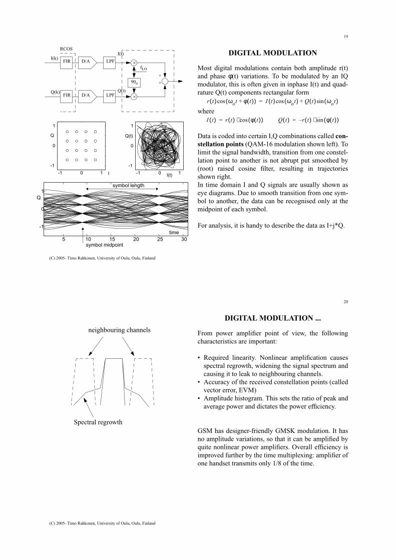
DIGITAL MODULATION
Most digital modulations contain both amplitude r(t)
and phase φ(t) variations. To be modulated by an IQ
modulator, this is often given in inphase I(t) and quad-
rature Q(t) components rectangular form
where
Data is coded into certain I,Q combinations called con-stellation points (QAM-16 modulation shown left). To
limit the signal bandwidth, transition from one constel-
lation point to another is not abrupt put smoothed by
(root) raised cosine filter, resulting in trajectories
shown right.
In time domain I and Q signals are usually shown as
eye diagrams. Due to smooth transition from one sym-
bol to another, the data can be recognised only at the
midpoint of each symbol.
For analysis, it is handy to describe the data as I+j*Q.
r t( ) ωot φ t( )+( )cos I t( ) ωot( )cos Q t( ) ωot( )sin+=
I t( ) r t( ) φ t( )( )cos⋅= Q t( ) r t( )– φ t( )( )sin⋅=
5 10 15 20 25 30
-1
0
1
-1 0 1
-1
0
1
-1 0 1
-1
0
1
I(t)I
Q(t)Q
time
Q
symbol midpoint
symbol length
FIR D/A LPF
90o
+
FIR D/A LPF
fLO
+
I(t)
Q(t)
I(k)
Q(k)
RCOS
20
(C) 2005- Timo Rahkonen, University of Oulu, Oulu, Finland
DIGITAL MODULATION ...
From power amplifier point of view, the following
characteristics are important:
• Required linearity. Nonlinear amplification causes
spectral regrowth, widening the signal spectrum and
causing it to leak to neighbouring channels.
• Accuracy of the received constellation points (called
vector error, EVM)
• Amplitude histogram. This sets the ratio of peak and
average power and dictates the power efficiency.
GSM has designer-friendly GMSK modulation. It has
no amplitude variations, so that it can be amplified by
quite nonlinear power amplifiers. Overall efficiency is
improved further by the time multiplexing: amplifier of
one handset transmits only 1/8 of the time.
Spectral regrowth
neighbouring channels
Page 11
21
(C) 2005- Timo Rahkonen, University of Oulu, Oulu, Finland
AMPLITUDE HISTOGRAM
Different constellation points may have different
amplitudes, and due to filtering, amplitude distribution
has a continuum of values. This means that the peak
power is typically much larger than the desired average
power. This ratio is called crest factor
and it simply means, that the amplifier needs to be able
to handle large peak powers. Especially in multi-car-
rier signals the crest factor is very large.
Very rare peak amplitudes can be clipped without seri-
ous harm. To find the probability of amplitudes
exceeding certain value, it is customary to plot the
cumulative density function (cpdf), 1-cpdf, or cpdf/(1-
cpdf) on a logarithmic scale.
For comparison, in FM r(t) is constant. In such con-
stant-envelope modulation amplifier nonlinearities do
not cause distortion products around the carrier. Hence,
these can be amplified by high-efficiency but nonlinear
switch-mode amplifiers.
CFPpeakPavg
---------------=
0 0.5 1 1.5 2 2.50
pdf r
(t)
0 0.5 1 1.5 2 2.510
-5
100
105
log
cpdf
r(t
)
r(t) V
r(t) V
r(t) rms
r(t) peak
0.001
0.001
pdf: propability density function
cpdf: cumulative propability density function
log cpdf: log10( cpdf/(1-cpdf) )- from this it is easy to find insignificant
min and max amplitudes
22
(C) 2005- Timo Rahkonen, University of Oulu, Oulu, Finland
EFFECTS OF DISTORTION
The spectrum of the distorted signal is much wider
than the original signal, overlapping also the neigh-
bouring channels. The effects of distortion are
described by two figures of merit:
Adjacent channel power (ACP). This explains what is
the amount of power leaking to the neighbouring chan-
nel, given in dBc, dB’s compared to the carrier power
Vector Error (EVM). This describes how much the in-
band distortion affects the constellation points
0 5 10-80
-60
-40
-20
0
SP
EC
TR
UM
510
Distortion
Signal
Adjacentchannel
Inband distortionAdjacent channel distortion
-1 0 1
-1
0
1
-1 0 1
-1
0
1
Page 12
23
(C) 2005- Timo Rahkonen, University of Oulu, Oulu, Finland
MEMORY EFFECTS
Here, memory effect simply means that the distortion
is somehow bandwidth dependent. Polynomial models
or plain AM-AM model are memoryless, resulting in
bandwidth-independent distortion. However, AM-AM
may show hysteresis, and a typical symptom is asym-
metry between the upper and lower IMD sidebands.
Memory effects are usually not harmful, but they
become a problem in cancelling linearising systems:
the shape of the cancelling signal needs to match
closely with the actual IMD spectrum. On the example
left, the achieved cancellation is bandwidth dependent,
and better on the upper side band.
Ampl_in / V
Am
pl_
ou
t /
V
distorted signal
cancelling signal (memoryless)
linearised signal
frequency
24
(C) 2005- Timo Rahkonen, University of Oulu, Oulu, Finland
CAUSES OF MEMORY EFFECTS
Typical cause of memory effects is the up or down-
conversion of 2nd order distortion from DC and 2nd
harmonic band. Distortion on these bands is shaped by
frequency-dependent bias and matching impedances,
and hence these components have frequency depend-
ency. Another common cause is self-heating, where the
temperature variations are shaped by the low-pass ther-
mal impedance.
Hence, IM distortion consists of broadband, memory-
less contributions caused e.g. by 3rd and 5th degree
nonlinearities, and up and down-converted products
that may have some frequency dependence (this is
illustrated left as a vector diagram of an IM3 tone).
Especially the up-conversion from DC band and elec-
tro-thermal memory may cause asymmetry, as it
appears at opposite phases in upper and lower IMD
sideband.
v
v2 = iNL2 Z(f)
v3
IM3total
3rd-order
envelope
2nd-harmonic
tone spacing in a 2-tone
test is varied
Page 13
25
(C) 2005- Timo Rahkonen, University of Oulu, Oulu, Finland
SINGLE-CARRIER VS. MULTI-CARRIER
Left, 1- and 2-carrier signals with the same total power
are driven into the same amplifier model.
In the 1-carrier signal it is seen that the nonlinearity
broadens the spectrum and distorts the constellation
diagram, but different symbols can still be recognised,
as the shift of the constellation points is systematic.
In the 2-carrier signal, the 1.4 times larger peak ampli-
tude clearly starts to compress, rounding the IQ trajec-
tory plot. More seriously, now the shift of the
constellation points is largely caused by the neighbour-
ing channel that has non-correlated signal. This makes
the EVM to look random.
Multi-carrier signals require a more linear amplifier
than single-carrier signals.
-1 0 1
-1
0
1
-1 0 1
-1
0
1
-1 0 1
-1
0
1
0 5 10 15
x 106
-80
-60
-40
-20
0
SP
EC
TR
UM
-1 0 1
-1
0
1
-1 0 1
-1
0
1
-1 0 1
-1
0
1
0 0.5 1 1.5 2 2.5 37
-80
-60
-40
-20
0
SP
EC
TR
UM
26
(C) 2005- Timo Rahkonen, University of Oulu, Oulu, Finland
3. LINEARISATION METHODS
Dimensioning
• Backoff
• Sweet bias points
Feedback
• Cartesian and polar feedback
Feedforward
• Efficiency issues
Predistortion
• BB digital/analog, IF, RF
High efficiency transmitters
• Doherty amplifier
• LINC / CALLUM
• Polar transmitter
Page 14
27
(C) 2005- Timo Rahkonen, University of Oulu, Oulu, Finland
-40 -30 -20 -10 0-80
-60
-40
-20
0
20
100
10
1
Fundamental
IM3Efficiency
IM3 spec
Po
dB
Pin dB
55 dB
Canc.
Effi
cien
cy %
REQUIRED AMOUNT OF LINEARISATION
28
(C) 2005- Timo Rahkonen, University of Oulu, Oulu, Finland
ACCURACY REQUIREMENTS OFCANCELLING SYSTEMS
One method of reducing distortion is to try to cancel it
with distortion equal in amplitude but opposite in
phase. However, the accuracy requirements for this are
quite tough. Using cosine rule to solve the error vector,
the achievable cancellation is
where δA and ∆φ are amplitude and phase errors, res-
pectively. For example, to achieve 30 dB reduction (1/
30 in amplitude) in distortion, amplitude error must be
less than 0.25 dB (3%) and phase error less than 1
degree. These requirements are similar but tougher
than for SSB upconverters.
CANC 10 1 2 1 dA A⁄+( ) ∆φ( )cos 1 dA A⁄+( )2+–( )log⋅=
0.1 1 10-60
-55
-50
-45
-40
-35
-30
-25
-20
-15
-10
0 dB
0.05 dB
0.1 dB
0.25 dB
0.5 dB
1 dB
2 dB
PHASE ERROR (DEGR)
CA
NC
EL
LA
TIO
N d
B
A (to be cancelled)
A+dA
∆φ
error
err2 A2 A ∆A+( )2 2A A ∆A+( ) ∆φ( )cos–+=
Page 15
29
(C) 2005- Timo Rahkonen, University of Oulu, Oulu, Finland
BACKOFF
Easiest way to improve linearity is to back off the input
power from the compression level. For linear modula-
tions, backoff equal to the crest factor is usually requi-
red.
Backoff results in serious over-dimensioning. For
example, if a 1W average output power is needed and
the backoff level is 10 dB, the peak power level of the
amplifier needs to be 10W. Unfortunately, 10 dB back-
off results in power efficiency of some percents, only.
-40 -30 -20 -10 0-80
-60
-40
-20
0
20
100
10
1
Fundamental
IM3Efficiency
IM3 spec
Po
dB
Pin dB
55 dB
Canc.
Effi
cie
ncy
%
Backoff
30
(C) 2005- Timo Rahkonen, University of Oulu, Oulu, Finland
SWEET BIAS POINTS
Many devices have certain bias points where the dis-
tortion is lower than could be expected from the 3x
linear trend.
These minima are often due to intra-device cancelling
mechanisms, and the various contributions of the IM3
of the gm element (Ids) and the total drain current (ID,
including also the current through drain capacitance)
are shown left. Some of the cancelling components are
frequnecy dependent, hence also the sweet spot may
depend on signal bandwidth, or center frequency.
Left are shown various contributions of a sweet spot in
an LDMOS transistor. Ids is the gm current source, Id
is the total drain node current, including capacitor cur-
rents. Kxy refers to a nonlinear term
Kxy*Vin^x*Vout^y (K10 is a linear term like Cds or
gm)
(Aikio: MTT-IMS 2005)
-30
-40
-50
-60
-70
-80
Id [
dB
]
genIM3(Ids)
K1(Ids)Vo1
ResultId/HB
K1(Cds)*Vo1
genIM3(Cds)
K1(Cgd)V1
100 200 300 400IDQ [mA]
IDQ for phasorpresentation
-30
-40
-50
-60
-70
Ids [
dB
]
-80
-90
K30Vi3K50Vi5
genIM3(Ids)K20VH2
K40Vi4
K10(Ids)Vi1
ResultIds/HB
K20VENV
K03Vo3
Vi1Vo1 K02Vo2
IM3 magnitude vs. bias current
Page 16
31
(C) 2005- Timo Rahkonen, University of Oulu, Oulu, Finland
FEEDBACK
Provided that the feedback path is linear, feedback
reduces distortion by the amount of loop gain - e.g. to
reduce distortion by 20 dB, we need loop gain of 20
dB.
• Basic principle by Black in 20’s
• Distortion in the forward branch is reduced by 1/T,
where T is the loop gain of the amplifier feedback
combination. Distortion in the feedback branch
appears directly in the output.
• Fundamental problem of using output that already
exists to correct the input that caused that distortion
-> works well only with periodic signals
• Stability and bandwidth issues
noise,distortion, ...
Vin Vout+
-
+
CA
NC
dB
Lo
op
gain
dB f 3dB f 0dB
foffset
32
(C) 2005- Timo Rahkonen, University of Oulu, Oulu, Finland
CARTESIAN FEEDBACK
At RF frequencies it is difficult to achieve very high
loop gain. One way to circumvent this is to form the
error signal at baseband and use quadrature up and
down conversion in the direct and feedback branches.
Problems:
• delay in mixers and PA reduce the achievable band-
width. Any propagation delay reduces the phase
margin directly by amount of
• needs very linear and low-noise feedback path
• power control needs to be arranged so that the loop
gain remains constant
Cartesian feedback is limited to systems with band-
widths of some tens of kHz. It is standardly used e.g. in
Tetra radios. Commonly, lead-lag or lag-lead compen-
sation is needed to ensure stability.
∆φ jωTD–( )exp=
LO
Baseband
I
Q
deep class AB
1 kHz 10 kHz 10 kHz 1 MHz 10 MHz
0.001
0.01
0.1
1
10
100
131030100300
30 degree limit
TD / ns
Offset frequency
Pha
se la
g de
gr
φ 360 f offs ∆T⋅ ⋅=
Page 17
33
(C) 2005- Timo Rahkonen, University of Oulu, Oulu, Finland
FEEDFORWARD
Feedforward is actually older invention than feedback
(Black @ Bell Labs, 1928).
• The distortion generated by the main amplifier A1 is
extracted, amplified by an auxiliary error amplifier
A2, and substracted from the output signal
• To achieve good cancellation in node B, the error
amplifier A2 needs to have flat frequency response
• Losses of the power splitters / combiners reduce the
overall efficiency
• Adaptation is tricky, requiring two amplitude and
phase tuning loops + accurate delay matching
Although feedforward is not very easy to adapt, it can
provide broadband linearisation and is suited for multi-
carrier signals.
B
A
A1
A2
34
(C) 2005- Timo Rahkonen, University of Oulu, Oulu, Finland
LOSSES AND EFFICIENCY
The upper picture shows the attenuation of the direct
signal as a function of the coupling in power splitters/
combiners. For example, two -10 dB couplers cause a
loss of 1 dB to the output of the main amplifier in a
feedforward amplifier.
The lower figure shows the total efficiency including
losses after the amplifier. For example, 1 dB losses are
sufficient to reduce original 40% efficiency down to
32%. 3 dB combiner losses would reduce the effi-
ciency to 20%.
Pdirect = Pin - Pcoupled
Efficiency = Pdirect / PDC
-20 -18 -16 -14 -12 -10 -8 -6 -4 -2 0-5
-4
-3
-2
-1
0
Coupling dB
P d
irect
dB
0 0.5 1 1.5 2 2.5 30
10
20
30
40
50
60
Total losses dB
Tota
l effi
cien
cy %
Pcoupled
Pdirect
Page 18
35
(C) 2005- Timo Rahkonen, University of Oulu, Oulu, Finland
PREDISTORTION
The basic idea of predistortion is to cancel the distor-
tion in the power amplifier by predistorting the trans-
mitted signal with the inverse function of the amplifier.
I.e. if the amplifier is driven to compression, higher
amplitudes need to be expanded to make the total res-
ponse linear.
This compensating nonlinearity makes the spectrum of
the transmitted signal wider, requiring higher sampling
rates, wider IF filters etc.
Note that any frequency dependence between the pre-
distorter and amplifier makes also the cancellation fre-
quency dependent.
PRED
36
(C) 2005- Timo Rahkonen, University of Oulu, Oulu, Finland
DIGITAL PREDISTORTION
Left is the most common digital predistorter structure.
Signal amplitude |r(t)| information is used to choose a
signal-dependent complex gain value from a look-up-
table (LUT), that is used to scale and rotate the signal
vector. Filter block H can be used to introduce memory
effects into predistortion signal. The LUT is slowly
adapted by a feedback loop that IQ downconverts the
linearised output signal.
Predistortion causes spectral regrowth. Hence, a higher
sampling frequency is needed. Also the frequency
response of all filters between the predistorter and the
amplifier needs to be very flat and linear-phase, or the
effects of these need to be corrected by H as well.
I + j*Q
|r(t)| LUTH
Digital
Page 19
37
(C) 2005- Timo Rahkonen, University of Oulu, Oulu, Finland
ANALOG PREDISTORTER
The connection left is sometimes used as a predistorter
to create controllable amount of IM3 in the input of the
PA. Both diodes are biased on, and due to the balanced
structure, 2nd order nonlinearity of the diodes is can-
celled. Thus, only IM3 is generated (mismatch in dio-
des creates residual IM2 ).
That kind of simple predistorters have been used e.g. in
satellite transmitters.
V
1
2
v2
iNL2 = K2(-v2)2
iNL3 = K3(-v2)3
iNL2 = K2(+v2)2
iNL3 = K3(+v2)3
PA
cancel
sum up
38
(C) 2005- Timo Rahkonen, University of Oulu, Oulu, Finland
DOHERTY AMPLIFIER
In Doherty amplifier the efficiency of the class AB or
B main amplifier is improved by using λ/4 impedance
transformer and a class C peak amplifier to control the
load resistance seen by the main amplifier: RLmain is
actively tuned so that the main amplifier remains at the
edge of compression for e.g. 1:2 input voltage range.
If Zomain, Zopeak >>, RLmain seen by the main
amplifier is
Inclusion of the output impedances Zomain, Zopeak
complicates this simple analysis.
The 90 degree phase shift in the main branch is com-
pensated by delaying the input of the peak amplifier by
T/4.
RLmain
Zo2
Ro 1I peakImain--------------+
------------------------------------=
Vin
Vout,mainRLmain
Ipeak
MAIN AMP PEAK AMP
Ro
Ζο, λ/4
Vout
Zomain >>
Zopeak >>
RLmain
Imain
Vout,main
(saturates, but themain amp powerstill increases)
Page 20
39
(C) 2005- Timo Rahkonen, University of Oulu, Oulu, Finland
LINC AND CALLUM TRANSMITTERS
In LINC an amplitude-varying signal is presented as a
vector sum of two constant-envelope signals, that are
phase modulated. Thus, the amplifiers can be e.g.
switched amplifiers.
Problems:
• Needs a low-loss combiner
• Spectral regrowth of v1 and v2 is huge. The
regrowth cancels in the summation, provided that the
branches match accurately
• In CALLUM, feedback is employed to improve the
accuracy of v1 and v2. However, then the signal sep-
aration will have an amplitude-dependent band-
width.
v1(t)
v2(t)
v1(t)
v2(t)
vout(t)
vout(t)
Sig
nal
sep
ara
tio
n
40
(C) 2005- Timo Rahkonen, University of Oulu, Oulu, Finland
POLAR TRANSMITTER
In polar transmitters, a power-effective switching
amplifier is driven by phase modulated constant enve-
lope carrier. The amplitude information as added by
modulating the power supply of the amplifier by a
modulated DC source.
The output distortion is very sensitive to time delay
between the amplitude and phase channels, as well as
sufficiently broad frequency response of the amplitude
channel. The bandwidth of the rectified amplitude
|A(t)| is roughly 3 times the baseband bandwidth, while
the CE phase modulated carrier has 5..6 times the
bandwidth of the original signal.
The same idea is applied in the EER transmitter (enve-
lope elimination and restoration), where RF amplitude
detectors and limiting amplifiers are used to separate
the amplitude and phase signals.
PM
|A(t)|
u t( ) A t( ) 2π f ot φ t( )+( )cos⋅=
|A(t)|
φ(t)