38
Power Electronics for Fuel Cell Based Power Generation Systems Allen Hefner NIST The Semiconductor Electronics Division (NIST/DOE Interagency Agreement)

Power Electronics for Fuel Cell Based Power Generation Systems
Allen HefnerNIST
The Semiconductor Electronics Division
(NIST/DOE Interagency Agreement)

Outline
I. IntroductionII. Technology Impact AnalysisIII. Component TechnologiesIV. Power Converter ArchitecturesV. Cost Estimates and Simulation

I. IntroductionObjective:• High-Megawatt Power Conditioning Systems (PCS) are
required to convert: – from power produced by Fuel Cells (FC) in future power plants – to very high voltage and power required for delivery to the grid
Motivation:• DoE SECA cost goals:
– FC generator plant $400/kW – including $40-100/kW for PCS
• Today’s PCS cost (Fuel Cell Energy Inc.):– FC generator plant $3,000/kW – including $260/kW for power converter (to 18 kV AC)
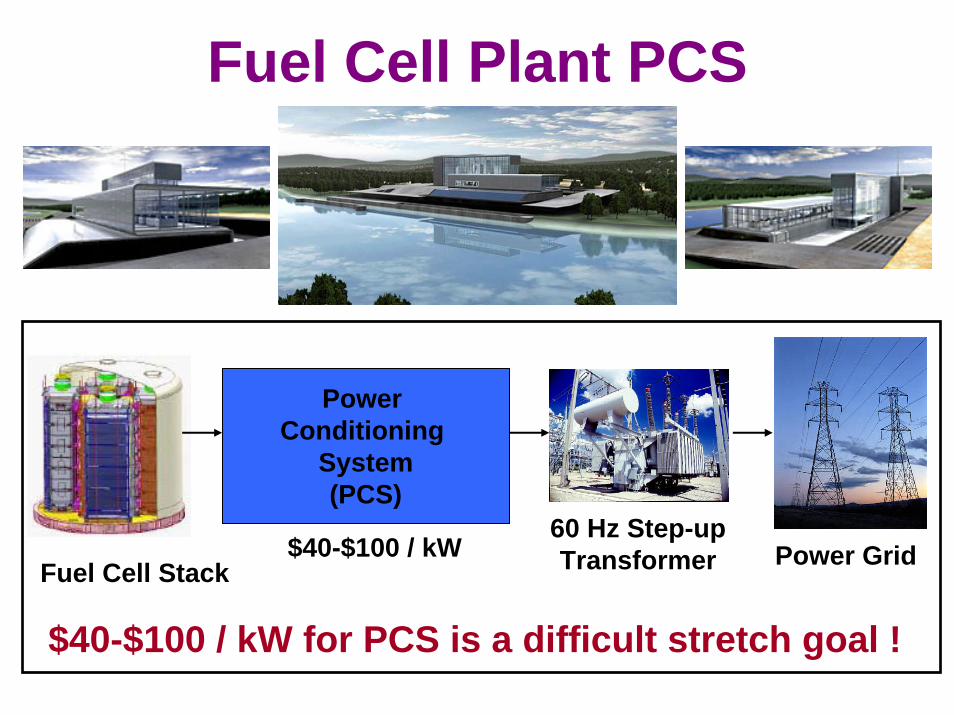
Fuel Cell Plant PCS
Power Conditioning
System(PCS)
Fuel Cell Stack60 Hz Step-upTransformer Power Grid
$40-$100 / kW for PCS is a difficult stretch goal !
$40-$100 / kW

• NIST/DOE Inter-Agency Agreement– NIST lead effort to determine expected impact of advanced
technologies on future FC power plant PCS
• Inter-Agency Power Group (IAPG)– Form an interagency task group for high-megawatt power
converter technologies under IAPG
• Industry Roadmap– Initiate a roadmap process to offer guidance for further
development of high-megawatt PCS technology
• National Science Foundation (NSF)– Establish power electronics curriculums and fundamental
research programs for energy systems technology
Federal and IndustryPCS Program Coordination

Outline
I. IntroductionII. Technology Impact AnalysisIII. Component TechnologiesIV. Power Converter ArchitecturesV. Cost Estimates and Simulation

II. Technology Impact Analysis• Perform Independent Analysis of technologies that
may reduce cost of PCS for future FC Power Plants
• Methodology for impact study:– Include input from broad power electronics, power
component, and power engineering communities– Classify power converter architectures, topologies, and
component technologies that may reduce cost – Perform tabular calculations of cost for each option using
estimated advantages of new technologies– Use component modeling, and circuit and system
simulations to verify and refine calculations

Methodology for Impact Analysis:
NIST Coordination
Architectures•ABB•Fuel Cell Energy•General Electric•Infineon•Siemens
Topologies•VA Tech FEEC•Satcon•Oak Ridge NL•Univ. Illinois
Semiconductors•CREE•NIST•Powerex
Power Converters•VA Tech FEEC•Los Alamos NL•Texas A&M•Oak Ridge NL
Cost Estimate Simulation
Passive Components•General Atomics•Los Alamos NL
High Megawatt Converter Workshop: http://www.high-megawatt.nist.gov/workshop-1-24-07/
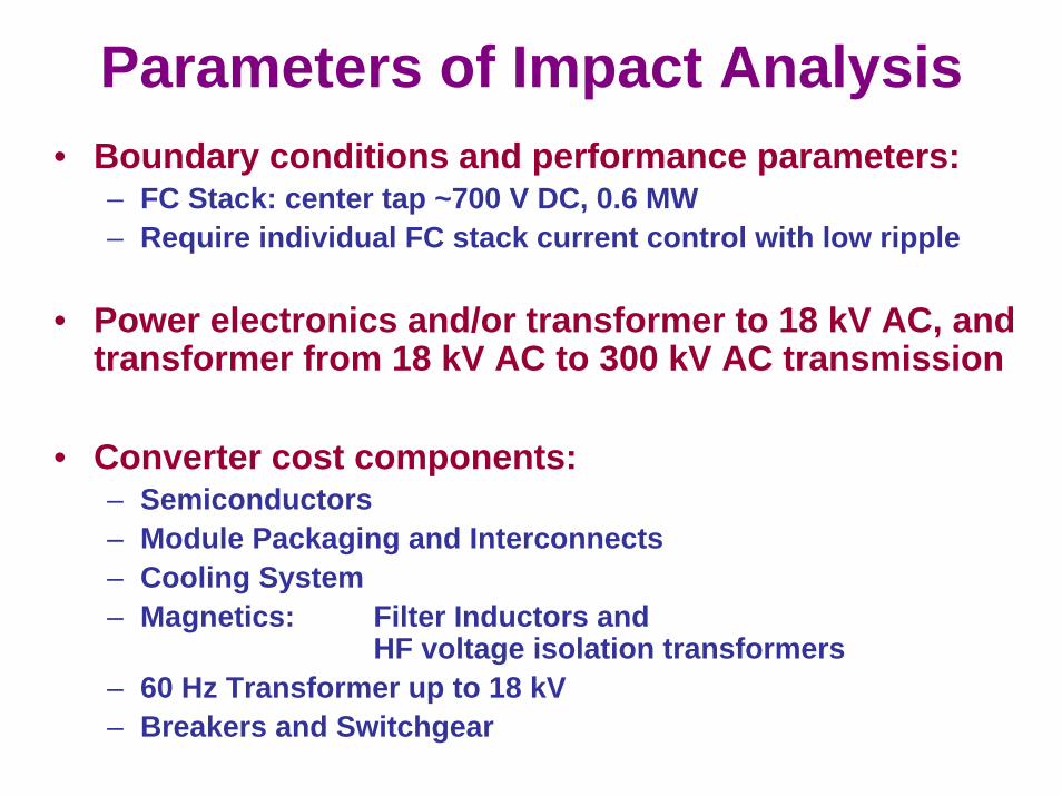
Parameters of Impact Analysis• Boundary conditions and performance parameters:
– FC Stack: center tap ~700 V DC, 0.6 MW– Require individual FC stack current control with low ripple
• Power electronics and/or transformer to 18 kV AC, and transformer from 18 kV AC to 300 kV AC transmission
• Converter cost components:– Semiconductors– Module Packaging and Interconnects– Cooling System– Magnetics: Filter Inductors and
HF voltage isolation transformers– 60 Hz Transformer up to 18 kV– Breakers and Switchgear

SemiconductorsPackaging and Interconnects
HF transformersFilter Inductors and Capacitors
Cooling System60 Hz Transformer up to 18 kV
Breakers and Switchgear
Ripple < 2%Stack Voltage Range~700 to 1000 VFuture: 2X voltage ?
$40-$100 / kW
300 MW PCS
IEEE – 519IEEE – 1547
Harmonic DistortionFuture: HVDC transmission ?
18 kVAC
300 kVAC
Approx. 500Fuel Cells
~700 VDC
~700 VDC

Outline
I. IntroductionII. Technology Impact StudyIII. Component TechnologiesIV. Power Converter ArchitecturesV. Cost Estimates and Simulation

A. Low-Voltage Semiconductors
• Baseline: 1200 V silicon IGBT with silicon PiN diode– 1200 V is sweet spot for silicon IGBTs at 15 – 20 kHz switching
due to speed voltage trade-off, high volume, and maturity– Mature technology; cost may not continue to decrease
• 1200 V silicon IGBT switch with SiC Schottky diode– More efficient at 20 kHz less loss, lower heat removal cost
lower temperature and longer life– Higher frequency less filter inductor cost– Emerging commercial technology; cost continues to decrease
– What is cost break-point for 1200 V SiC Schottky diode?

B. High-Frequency Transformer• Baseline: Traditional Ferrite Material
– Expensive processing for high-power, high frequency (HF)– Mature technology; cost may NOT decrease
• HF magnetic materials: Nano-crystalline or Metglas®
– Size and cost decrease inversely proportional to frequency– Emerging commercial technology; cost continues to decrease
– What is cost break-point for HF magnetic material?
10 100 103 104 105
10-3
10-2
10-1
1
10
Frequency (Hz)
Cor
e Si
ze
10-4
10-5
10-6
60 Hz 20 kHz10 100 103 104 105
10-3
10-2
10-1
1
10
Frequency (Hz)
Cor
e Si
ze
10-4
10-5
10-6
60 Hz 20 kHz

C. High-Voltage Semiconductors • Baseline: High-Voltage (HV) Silicon devices (IGBT, IGCT)
– Typically ~6.5 kV blocking voltage maximum– Requires multi-level inverter for 4160 V AC – Low switching frequency (< 500 Hz) requires larger filter
• High-Voltage, High-Frequency SiC Switch and Diodes12 kV, 20 kHz SiC MOSFET switch and SiC Schottky diode:
– Less inverter levels due to higher voltage – Less loss, lower heat removal cost– Less filter inductance required due to higher frequency
15 kV, 5 kHz SiC IGBT switch and SiC PiN diode:– Higher current per die than SiC MOSFET, therefore lower cost
– What is cost break point for HV-HF SiC power semiconductors?
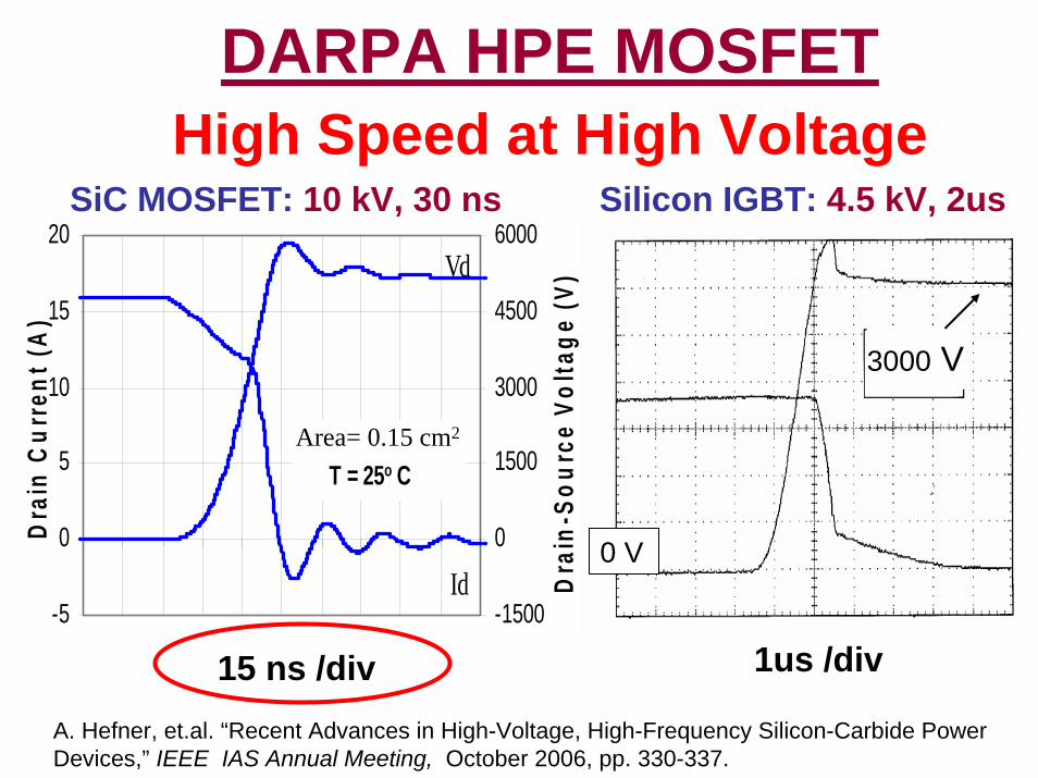
DARPA HPE MOSFET High Speed at High Voltage
-5
0
5
10
15
20
Dra
in C
urre
nt (A
)
-1500
0
1500
3000
4500
6000
Dra
in-S
ourc
e Vo
ltage
(V)
Area = 0.125 cm2
T = 25o C
Vd
Id
SiC MOSFET: 10 kV, 30 ns Silicon IGBT: 4.5 kV, 2us
1us /div
3000 V
15 ns /div
0 V
Area= 0.15 cm2
A. Hefner, et.al. “Recent Advances in High-Voltage, High-Frequency Silicon-Carbide Power Devices,” IEEE IAS Annual Meeting, October 2006, pp. 330-337.

Outline
I. IntroductionII. Technology Impact StudyIII. Component TechnologiesIV. Power Converter ArchitecturesV. Cost Estimates and Simulation

IV. Power Converter ArchitecturesA. Low-Voltage Inverters (460 V AC):
– Require high current for each 0.6 MW FC– and large number of Inverters for 300 MW Plant
B. Medium-Voltage Inverters (4160 V AC):– Lower inverter current for each 0.6 MW FC– Combine multiple FCs with single high power inverter
C. High-Voltage Inverters (18 kV AC):– Replaces 60 Hz transformer with isolation from HF transformer – Cascade enables: 18 kV AC inverter by series connection, and
interleaved switching decreases losses and filter requirement

A. Low-Voltage Inverters480 V AC Inverter,
60 Hz Transformer to 18 kV AC
1) First Generation: ~350 V FC, DC-DC to 750 V, 480 V AC Inverter
2) Baseline: ~700 V FC (center tap), DC-DC to 750 V,480 V AC inverter
– 1200 V is “Sweet spot” for silicon semiconductors due to market size and speed voltage trade-off
3) Present Generation: ~700 V FC, 480 V AC Inverter– Fewer semiconductors due to single stage converter
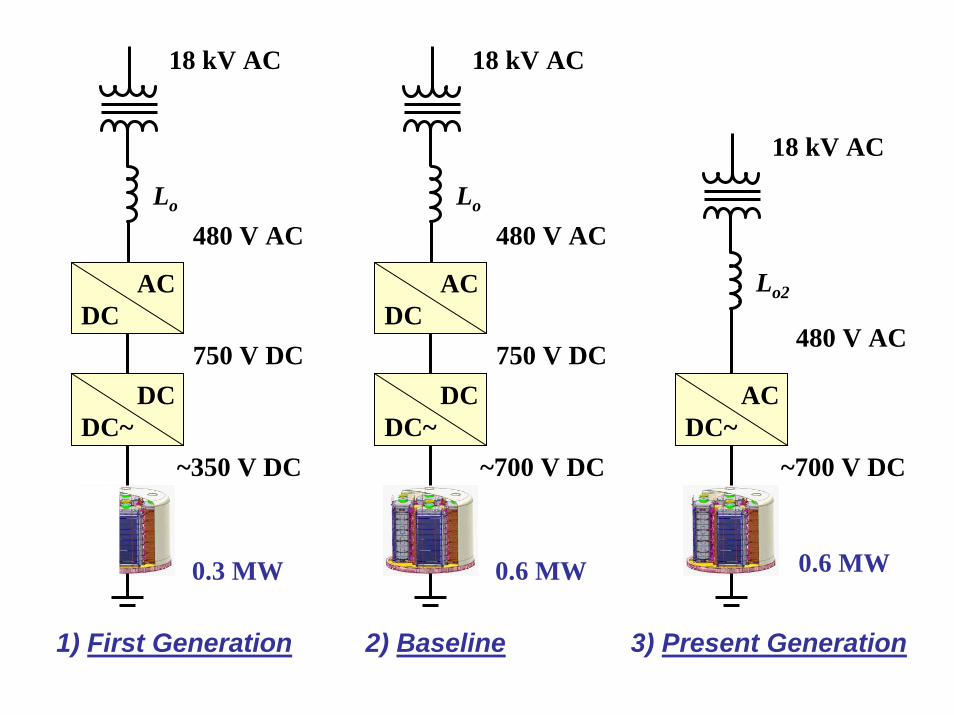
Lo
480 V AC
~350 V DC
DCDC~
ACDC
750 V DC
18 kV AC
Lo
480 V AC
~700 V DC
DCDC~
ACDC
750 V DC
18 kV AC
Lo2
480 V AC
~700 V DC
ACDC~
18 kV AC
1) First Generation 2) Baseline 3) Present Generation
0.3 MW 0.6 MW 0.6 MW

B. Medium Voltage Inverters4160 VAC Inverter
60 Hz Transformer to 18 kV AC
MV DC Common Bus:
LV-to-MV DC-DC converters:– Requires high voltage-gain DC-DC converter, HF transformer– HV SiC diode rectifiers substantially reduce loss !
Common MV inverter:– Silicon semiconductors require multiple levels for MV– HV SiC semiconductors provide lower switching loss

Lo
4160 V AC
~700 V DC
DCDC~
ACDC
MVDC Common Bus
18 kV AC
1) MV DC Common Bus: LV-to-MV DC-DC, Common Inverter
~700 V DC
DCDC~
DCDC~
… ~700 V DC
6750 V DC
High Voltage Gain DCDC Converter
0.6 MW
#1 #2 #8
MV Inverter4.6 MW

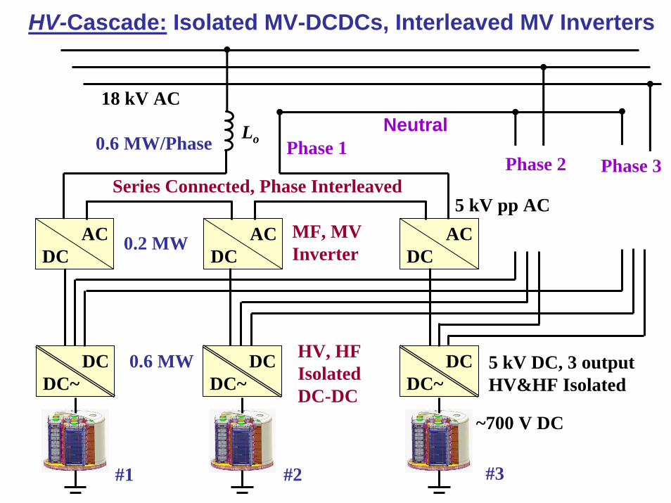
C. High Voltage Inverters18 kV AC Inverter,
No 60 Hz Transformer !
High-Voltage Cascade:
Series connected, voltage-isolated LV-to-MV DC-DC– Requires HV-HF isolation and output for each phase
Medium-Frequency, phase-interleaved invertersY-Configuration:
– 6.5 kV Silicon semiconductors require 6 levels– 12 kV SiC semiconductors require 3 levels
Lo
18 kV AC
DCDC~
ACDC
Series Connected, Phase Interleaved
HV-Cascade: Isolated MV-DCDCs, Interleaved MV Inverters
DCDC~
DCDC~
~700 V DC
0.6 MW/Phase
#3
5 kV DC, 3 outputHV&HF Isolated
HV, HF Isolated DC-DC
0.6 MW
#1 #2
ACDC
ACDC
5 kV pp ACMF, MVInverter0.2 MW
Phase 1Phase 3Phase 2
Neutral

Outline
I. IntroductionII. Technology Impact AnalysisIII. Component TechnologiesIV. Power Converter ArchitecturesV. Cost Estimates and Simulation

V. Cost Estimates and SimulationA. Cost Estimate: Tabular calculation of cost for each
PCS option using estimated advantages of newtechnologies
B. Simulation: Component modeling, and circuit andsystem simulations to verify and refine calculations
• Physics based models for component technologies• Simulation schematics for power converter topologies
Cost Estimate Simulation

A. Tabular Calculations of Cost• Future, high-volume costs: 5 to 10 years, 1 GW/yr
• Advanced Technology Goals and Cost Break Points– 1.2 kV Schottky diodes: $0.2/A– 12 kV Schottky diodes: $1/A– 12 kV Half-bridge SiC-MOSFET/SiC-Schottky: $10/A– 15 kV SiC-PiN: $0.4/A– 15 kV SiC-IGBT/SiC-PiN Module: $3.3/A– Nano-crystalline transformer: $2/kW– Power Electronics DC-DC, DC-AC: 150 % overhead– 60Hz Transformer and Switchgear: 50 % overhead

$0$20$40$60$80
$100$120$140$160$180$200Transformer &
SwitchgearOther PE
Semiconductor
Cooling
Magnetics
Inverter Voltage Low Low Low Low LowConverter Stages One One Two Two TwoLV-SiC Schottky yes yes
yes
yes yesHF Transformer Ferrite Nano60 Hz Transformer yes yes yes yes
Preliminary $/kW: LV Inverter
Risk Level: HighConsiderableModerateLow

$0$20$40$60$80
$100$120$140$160$180$200Transformer &
SwitchgearOther PE
Semiconductor
Cooling
Magnetics
Inverter Voltage Medium Medium High High HighHV-SiC Diode Schottky Schottky Schottky PiNHV-SiC Switch MOSFET MOSFET IGBTHF Transformer Nano Nano Nano Nano Nano60 Hz Transformer yes yes
Preliminary $/kW: MV & HV Inverter
Risk Level: HighConsiderableModerateLow
loss
loss

B. Component Modeling, Circuit and System Simulations• Physics based models developed for advanced
component technologies– 12 kV SiC Junction Barrier Schottky Diode (JBS)– 12 kV SiC Power MOSFET– 1200 V SiC Junction Barrier Schottky Diode (JBS)
• Models validated for static and switching characteristics
• Simulation schematics for power converter topologies

Model Validation for 12 kV, 100 ASiC Junction Barrier Schottky Diode
-40.0
-20.0
0.0
20.0
40.0
60.0
80.0
100.0
120.0
140.0
2.0E-07 4.0E-07 6.0E-07 8.0E-07 1.0E-06 1.2E-06 1.4E-06 1.6E-06Time [s]
Ano
de C
urre
nt [A
]
-8000
-7000
-6000
-5000
-4000
-3000
-2000
-1000
0
1000
Ano
de-C
atho
de V
olta
ge [V
]
Measured 15 A/us Simulated 15 A/us Measured 32 A/us
Simulated 32 A/us Measured 67 A/us Simulated 67 A/us
T = 25 ºC
Voltages
Currents
Forward Characteristics Reverse Recovery Switching

Model Validation for 12 kV, 100 A SiC Power MOSFET
Forward Output Characteristics Inductive Load Switching

Neutral
…Lo
ACDC
HF Transformer versus 60 Hz Transformer
ACDC
ACDC
HV Cascade Inverter Phase 1
3 Output DC-DC #1
Optional DC-DC
Lo
DCDC~
ACDC
18 k VAC60 Hz Transformer
…
LowVoltage Inverter
18 k VAC
HF Transformer
Rectifier RectifierRectifier
Inverter
Low Voltage Inverter Schematic
cba
480 Vl-l277 Vl-n
Vdc
ean
ebn
ecn
700 Vto
1 kV
ic
ia
ib
18 kVl-l10.4 kVl-n
FuelCell0.6 MW n
LineSwitchgear
TransformerSwitchgear
Plant DistributionLine

Lower Voltage Inverter Simulations
Output currents
Inverter output line-line voltage
Output phase-neutral voltage
Inverter output phase-neutral voltage
Time
75ms 80ms 85ms 90ms 95ms 100msI(La2) I(Lb2) I(Lc2)
-1.2KA-0.6KA
0A0.6KA1.2KA
V(Ea:+)-V(Ea:-) V(Eb:+)-V(Eb:-) V(Ec:+)-V(Ec:-)-400V
0V200V400V
SEL>>
V(VaL)-V(VbL)-1.0KV-0.5KV
0V0.5KV1.0KV
V(VaL)-V(vn)-500V-250V
0V250V500V
Time (ms)2015105 25
ia icib
van
ean ebn ecn
1.2 kA
1 kV
–1.2 kA
0
–500 V
500 V
–1 kV
–400 V
400 V
0
0
0
0
vab
20 kHz
750 V
High-Voltage Y-Connected Cascade Inverter Schematic
+–
van vbn vcn
ean
ic
ebn
+–
+–
ia
ib
+–
+–
+–
+–
+–
+–
Plant DistributionLine
ecn
LineSwitchgear
High-Voltage Y-Connected Cascade Inverter Simulation
total inverter output phase voltage
3 levels
1 level
Time
75ms 80ms 85ms 90ms 95ms 100msI(Rao) I(Rbo) -I(Rao)-I(Rbo)
-400A-200A
0A200A400A
V(Vo+)-V(Vao4) V(Vbo+)-V(Vbo4) V(Vao4)+V(Vbo4)-V(Vo+)-V(Vbo+)-1.5KV
-0.5KV
0.5KV
1.5KVV(Vao1)-V(Vao4)
-1.5KV
0.5KV
1.5KV
SEL>>
V(Vao1)-V(Vao2)-500V-250V
0V250V500V
Time (ms)2015105 25
ia icib
ean ebn ecn
400 A
0
15 kV
–400 A
0
–5 kV
5 kV
–15 kV
–15 kV
15 kV
0
0
(1 kHz switching)0
(eq. 3 kHz switching)
inverter 1 output voltage
utility phase voltage
output currents
van
va1
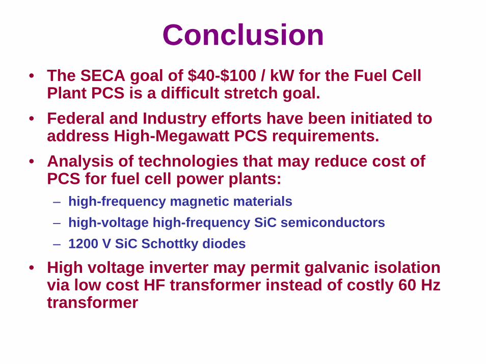
Conclusion• The SECA goal of $40-$100 / kW for the Fuel Cell
Plant PCS is a difficult stretch goal.• Federal and Industry efforts have been initiated to
address High-Megawatt PCS requirements. • Analysis of technologies that may reduce cost of
PCS for fuel cell power plants:– high-frequency magnetic materials– high-voltage high-frequency SiC semiconductors– 1200 V SiC Schottky diodes
• High voltage inverter may permit galvanic isolation via low cost HF transformer instead of costly 60 Hz transformer

AcknowledgmentsI would like to acknowledge Sam Biondo (DOE-Fossil Energy), Don Collins (DOE - NETL), Wayne Surdoval (DOE-NETL), Frank Holcomb (ERDC-CERL), Ron Wolk(Consultant), Heather Quedenfeld (DOE - NETL), and Jason Lai (VT-FEEC) for organizing activities to address PCS needs for fuel cell power plants, and in addition the participants ofthe Workshop on High Megawatt Converters for providing technical guidance.
I would also like to acknowledge Jason Lai (VT-FEEC), HaoQian (VT-FEEC), Angel Rivera-López (NIST), Tam Duong (NIST), José M. Ortiz-Rodríguez (NIST), Colleen Hood (NIST), and Robert Michelet (NIST) for technical contributions to the presented PCS cost analysis effort.


