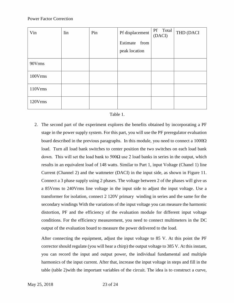
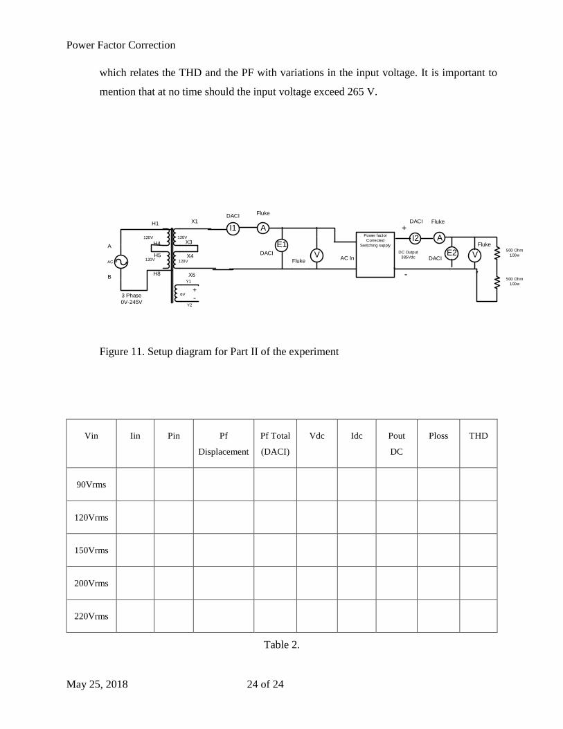
Power Factor Correction May 25, 2018 1 of 24 EXPERIMENT Power Factor Correction Power Factor Correction Requirements OBJECTIVE The objective of this module is to enhance the importance of power factor correction (PFC) by exploring some concepts related to standards, total harmonic distortion (THD) and PFC circuits. REFERENCES 1. “Fundamentals of Power Electronics,” First Edition, Robert W. Erickson, Chapman & Hall, 1997, Part IV. 2. “Switching Rectifiers for Power Factor Correction,” Volume V, Edited by Fred C. Lee, and Dušan Borojević, VPEC Publication Series, 1994. 3. IEC 61000-3-2, “Electromagnetic Compatibility (EMC) – Part 3-2: Limits for Harmonic Current Emissions (Equipment Input Current 16A per phase),” Edition 2.1, 2001-10. 4. M. M. Jovanović and D. E. Crow, “Merits and Limitations of Full-Bridge Rectifiers with LC Filter in Meeting IEC 1000-3-2 Harmonic Limit Specifications,” in IEEE Trans. On Industry Applications, Vol. 33, No.2, pp. 551-557, March/April 1997. 5. J. Sebastian, J. A. Cobos, J. M. Lopera and J. Uceda, “The Determination of the Boundaries Between Continuous and Discontinuous Modes in PWM DC-to-DC Converters Used as Power Factor Preregulators,” in IEEE Trans. on Power Electronics, Vol. 10, No. 5, pp. 574-582, September 1995. 6. L. H. Dixon, “High Power Factor Preregulator for Off-Line Power Supplies,” in Proc. Unitrode Power Supply Seminar, 1998, pp. 6.1-6.16. BACKGROUND INFORMATION As predicted by the Electric Power Research Institute (EPRI), more than 60% of utility power will be processed through some form of power electronics equipment by the year 2010. However, most of that equipment generates pulsating currents to the utility grids with poor power quality and high harmonic contents that adversely affect other users.
Transcript
Power Factor Correction
May 25, 2018 1 of 24
EXPERIMENT Power Factor Correction
Power Factor Correction Requirements
OBJECTIVE
The objective of this module is to enhance the importance of power factor correction (PFC) by
exploring some concepts related to standards, total harmonic distortion (THD) and PFC circuits.
REFERENCES
1. “Fundamentals of Power Electronics,” First Edition, Robert W. Erickson, Chapman & Hall,
1997, Part IV.
2. “Switching Rectifiers for Power Factor Correction,” Volume V, Edited by Fred C. Lee, and
Dušan Borojević, VPEC Publication Series, 1994.
3. IEC 61000-3-2, “Electromagnetic Compatibility (EMC) – Part 3-2: Limits for Harmonic
Current Emissions (Equipment Input Current 16A per phase),” Edition 2.1, 2001-10.
4. M. M. Jovanović and D. E. Crow, “Merits and Limitations of Full-Bridge Rectifiers with LC
Filter in Meeting IEC 1000-3-2 Harmonic Limit Specifications,” in IEEE Trans. On Industry
Applications, Vol. 33, No.2, pp. 551-557, March/April 1997.
5. J. Sebastian, J. A. Cobos, J. M. Lopera and J. Uceda, “The Determination of the Boundaries
Between Continuous and Discontinuous Modes in PWM DC-to-DC Converters Used as Power
Factor Preregulators,” in IEEE Trans. on Power Electronics, Vol. 10, No. 5, pp. 574-582,
September 1995.
6. L. H. Dixon, “High Power Factor Preregulator for Off-Line Power Supplies,” in Proc. Unitrode
Power Supply Seminar, 1998, pp. 6.1-6.16.
BACKGROUND INFORMATION
As predicted by the Electric Power Research Institute (EPRI), more than 60% of utility power will
be processed through some form of power electronics equipment by the year 2010. However, most
of that equipment generates pulsating currents to the utility grids with poor power quality and high
harmonic contents that adversely affect other users.
Power Factor Correction
May 25, 2018 2 of 24
The situation has drawn the attention of regulatory bodies around the world. Governments are
tightening regulations, setting new specifications for low harmonic current, and restricting the
amount of electro-magnetic waves that can be emitted.
Through this module, the student will become familiar with the importance of PFC in electronic
equipment by exploring some concepts related to standards, THD and PFC circuits.
Definitions
The power factor (PF) is defined as the ratio between the average power (averaged in a line period)
and the product of the rms values of the input voltage and current; that is,
TT
T
dttiT
dttvT
dttitvT
powerapparent
poweraveragePF
0
2
0
2
0
)(1
)(1
)()(1
, (1)
where v(t) and i(t) are, respectively, the input voltage and current waveforms and T is the line
period.
The THD is defined as
1
2
2
I
I
THDn
n
, (2)
where In and I1 are the amplitudes of the nth harmonic component and of the fundamental
component, respectively, of the line current i(t). The relationship between PF and THD can be
determined by defining the distortion factor as follows:
2)(1
1
THDDPF
PF
, (3)
where DPF is the displacement factor, which is equal to the well-known “cosine of ” when the
line voltage is sinusoidal, being the angle by which the fundamental component of i(t) lags v(t).
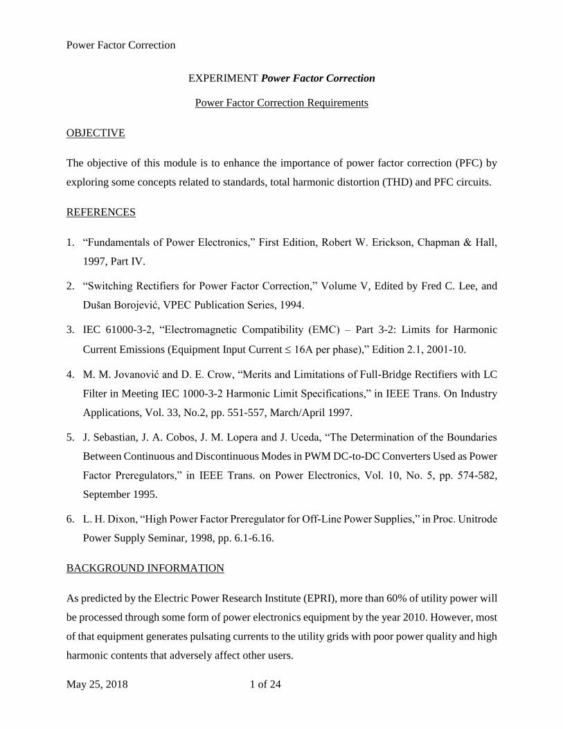
This relationship is plotted in Figure 1. The distortion factor of a waveform with a moderate
amount of distortion is quite close to the unity. For example, if the waveform contains a third
harmonic whose magnitude is 10% of the fundamental, the distortion factor is 99.5%. Increasing
Power Factor Correction
May 25, 2018 3 of 24
the third harmonic to 20% decreases the distortion factor to 98%, and a 33% harmonic magnitude
yields a distortion factor of 95%. So the PF is not significantly degraded by the presence of
harmonics unless the harmonics are quite large in magnitude.
Figure 1. Relationship between total harmonic distortion and distortion factor.
The Off-Line Rectifier
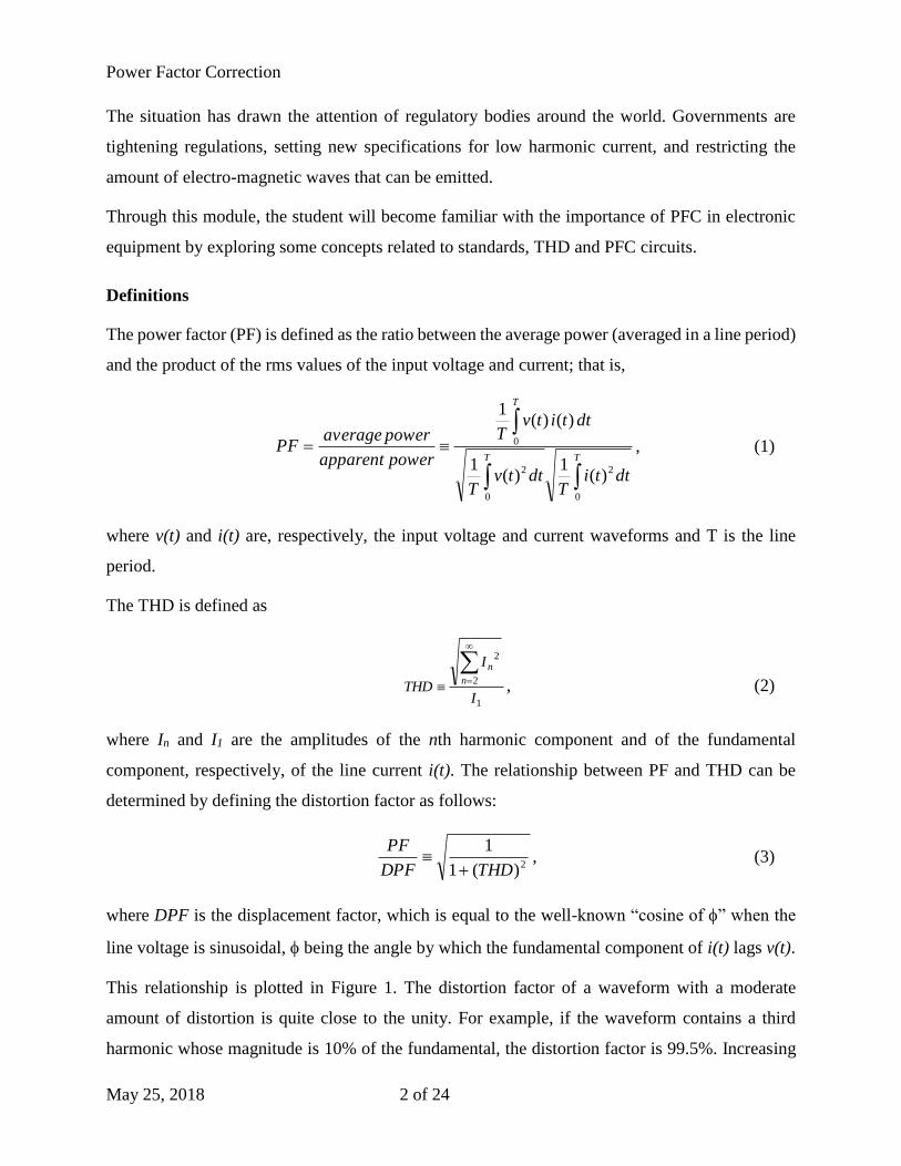
The conventional input stage of an off-line switching power supply design is shown in Figure 2(a).
It is comprised of a full-bridge rectifier followed by a large-input-filter capacitor. This input-filter
capacitor reduces the ripple on the voltage waveforms into the DC converter stage. The problem
with this input circuit is that it produces excessive peak input currents and high harmonic distortion
on the line. The high distortion in the input current occurs due to the fact that the diode rectifiers
only conduct during a short interval. This interval corresponds to the time when the mains
instantaneous voltage is greater than the capacitor voltage. Since the capacitor must meet hold-up
time requirements (during fault conditions, the mains are disconnected from the circuit for some
cycles) its time constant is much grater than the frequency of the mains. Therefore, the mains
instantaneous voltage is greater than the capacitor voltage only for very short periods of time,
during which, the capacitor must be charged fully. Therefore, large pulses of current are drawn
from the line over a very short period of time, as shown in Figure 2(b). This is true for all rectified
AC sinusoidal signals with capacitive filtering; they draw high amplitude current pulses, the
fundamental current of the line current is essentially in phase with the voltage, and the
displacement factor is close to the unity. However, the low-order current harmonics are quite large,
close to that of the fundamental. A typical current spectrum is shown in Figure 3. The THD for
this kind of rectification is usually in the range 55% to 65%. The resulting PF is similar in value.
0% 20% 40% 60% 80% 100%70%
80%
90%
100%
Total Harmonic Distortion
Dis
tort
ion F
acto
r
0% 20% 40% 60% 80% 100%70%
80%
90%
100%
Total Harmonic Distortion
Dis
tort
ion F
acto
r
Power Factor Correction
May 25, 2018 4 of 24
(a)
(b)
Figure 2. (a) Typical input stage for an off-line switching power supply and (b) main waveforms.
Figure 3. Typical AC line current spectrum for the input stage of an off-line switching power supply.
However, as can be seen, this system has many disadvantages:
It creates harmonics and electromagnetic interference (EMI).
It produces high losses.
It requires over-dimensioning of parts.
It reduces maximum power capability from the line.
CbulkMains
Inputs
CbulkMains
Inputs
Mains Input Voltage
Rectified Line Voltage
Capacitor Voltage
Diode Current
Main Input Current
Mains Input Voltage
Rectified Line Voltage
Capacitor Voltage
Diode Current
Main Input Current
100%
91%
73%
52%
32%
19%15% 15% 13%
9%
0%
20%
40%
60%
80%
100%
1 3 5 7 9 11 13 15 17 19
Harmonic number
Ha
rmo
nic
am
plit
ud
e,
pe
rce
nt
of
fun
da
me
nta
l THD = 136%
Distortion factor = 59%
Displacement factor = 1
PF = 59%
100%
91%
73%
52%
32%
19%15% 15% 13%
9%
0%
20%
40%
60%
80%
100%
1 3 5 7 9 11 13 15 17 19
Harmonic number
Ha
rmo
nic
am
plit
ud
e,
pe
rce
nt
of
fun
da
me
nta
l
100%
91%
73%
52%
32%
19%15% 15% 13%
9%
0%
20%
40%
60%
80%
100%
1 3 5 7 9 11 13 15 17 19
Harmonic number
Ha
rmo
nic
am
plit
ud
e,
pe
rce
nt
of
fun
da
me
nta
l THD = 136%
Distortion factor = 59%
Displacement factor = 1
PF = 59%
Power Factor Correction
May 25, 2018 5 of 24
Conventional AC rectification is thus a very inefficient process, resulting in high electricity cost
for the utility company and waveform distortion of the current drawn from the mains. It produces
a large spectrum of harmonic signals that may interfere with other equipment. A circuit similar to
that shown in Figure 2(a) is used in most mains-powered conventional and switch mode power
supplies. At higher power levels (200 to 500 watts and higher) severe interference with other
electronic equipment may become apparent due to these extra harmonics reflected back into the
power utility line. Another problem is that the power utility line cabling, the installation, and the
transformer must all be designed to withstand these peak current values.
Problems of Low Power Factor and High Harmonic Distortion
This section briefly presents some of the problems related to low PF and high harmonic distortion.
Less Useful Power Available
The power utility line circuit is designed, rated and fused based on the amount of current
that it can safely deliver. Since low PF increases the apparent current from the source, the amount
of useful power that can be drawn from the circuit is lowered due to thermal limitation. We will
use as an example the 120V 15A outlet circuit commonly found in offices and homes in the United
States. If we assume that the overall efficiency of the power conversion system inside the
equipment is 80% and that the line current is derated by 20% to avoid nuisance tripping, then the
useful power available from such a circuit, assuming a unity power factor (best possible case), can
be calculated as:
Pomax = 120V x (15A x 0.80) x 0.80 = 1152 watts.
Repeating the calculation using the uncorrected PF of 0.59 that we calculated in the previous
section, we obtain the maximum available useful power to be:
Pomax = 120V x (15A x 0.80) x 0.59 x 0.80 = 680 watts.
Note the enormous decrease in available load power. The low PF could have been caused by either
a phase-shift (displacement) or harmonic distortion with an equally devastating impact on the level
of useful power.
Power Factor Correction
May 25, 2018 6 of 24
AC Distributed Cost
Low PF increases not only the apparent line current but also the additional current capacity cost
money. This starts within the equipment itself and extends all the way back to the generation and
distribution systems of the electric utility. Wire sizes within the equipment and the building must
be increased to carry the additional current. When there is an abundance of loads with poor PF,
this need for increased capacity will require additional power generation and distribution capability.
This cost increase will, to a first approximation, be directly proportional to the inverse of the PF:
factorpowercapabilitypoweradditionalofCost
1 .
Thus, if all connected loads had a PF of 0.59 rather than 1, the increase in the hardware cost for
supplying the additional current would be approximately 69%. The power losses in any dissipative
circuit elements (such as wire connections and transformer windings) will be proportional to
square of the apparent current. Therefore, cost associated with providing this dissipated power will
also scale inversely with the PF. Utility meters in residential and office environments will actually
only register the real power drawn from the power utility line, so that the user is not directly
penalized in terms of utility costs for the reactive components of the power.
Voltage Waveform Distortion
For the purpose of simplicity, most of the calculations have assumed that the AC source impedance
is zero and the AC voltage waveform is not distorted by nonlinear current waveforms. In reality,
the source impedance, while low, is not zero. For fault protection purposes, the conductor sizes
get smaller as the AC power gets closer to the final load electronics. The smallest conductors are
within the equipment itself, and high level of distortion on the current waveform will start to affect
the quality of the voltage waveform, making it non-sinusoidal. If this voltage distortion becomes
severe, it can cause operational problems with the power supply and with other nearby equipment
connected to the same power source.
EMC
The higher line current associated with poor PF, especially if distortion and higher-frequency
harmonics are present, can make for a much more difficult electromagnetic compatibility (EMC)
environment. Passive PFC solutions often entail adding a capacitor, which often also acts as an
Power Factor Correction
May 25, 2018 7 of 24
EMC filter to reduce noise imposed onto the power utility line. Active PFC approaches can be a
source of additional switching activity and associated EMC. However, this noise is high frequency
in nature and can be controlled by filters utilizing physically small components, often at only one
location in the power system.
Three-Phase System
While we are focusing our attention on single-phase systems, the problem of harmonic distortion
in some three-phase systems should be mentioned. Specifically, a four-wire three-phase system
containing a neutral conductor can be severely compromised by harmonic current content on its
load. Loads that are not balanced from phase to phase will result in undesired neutral current
content. But even in the best case of completely balanced loads, harmonic contents in the loads
will appear in the neutral conductor. The good news is that most of the harmonics (including the
fundamental) will cancel out and will not result in a net current in the neutral conductor. The bad
news is that the so-called “triple” harmonics (3rd, 6th, 9th….) will appear and be directly
accumulative in the neutral conductor. For example, if the three loads each only contained a 3rd
harmonic that was 15% of the fundamental, the neutral would experience a 3rd harmonic current
equal to 45% of the fundamental current. Since the neutral conductors are sized according to the
assumption that they will conduct minimal current, this will create a significant problem for the
power system.
Regulatory Non-Compliance
Because of the problems cited above, all industrialized countries have established regulations and
standards that address PF and harmonic distortion on their power utilities; these will be addressed
in the next section. Without compliance to the appropriate standard(s), the off-line power supply
with conventional input rectifier will have a difficult time gaining acceptance in the market. In fact,
it may be illegal to attempt to sell it. These legal’ and profit-related issues make it mandatory that
power system designers understand the PF and current distortion potential of their designs and also
appropriate methods for making them compliant.
PFC techniques are being increasingly used in new off-line power converter designs. This is
motivated both by the concerns listed above and by regulatory requirements, and is overall a
positive development for equipment users and the power utilities. Most PFC circuits are now active
rather than passive, and while this results in exceptional PFC performance, it requires that
Power Factor Correction
May 25, 2018 8 of 24
additional circuitry be added. The added circuitry can have the following negative impacts on the
system:
Additional cost and complexity for the power converter
Lower power converter reliability
Slightly lower efficiency (additional conversion stage sometimes needed)
In spite of these potential limitations, including active PFC is most often a very good design
tradeoff for the power system. The above concerns are usually more than offset by the reduced
input current, undistorted current waveforms, and additional useful power capability of converters
that utilize PFC.
Active PFC
Improvements in the PF and harmonic distortion can be achieved by modifying the input stage of
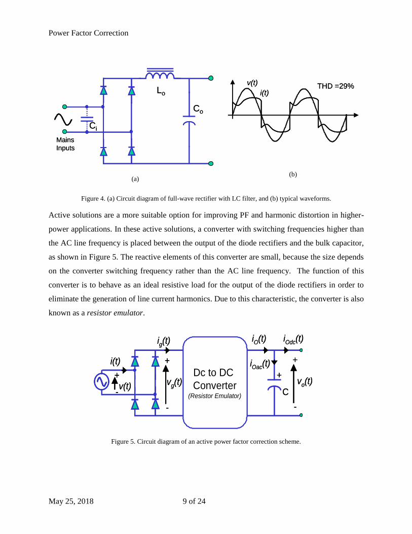
the off-line converter shown in Figure 2. Passive solutions (as shown in Figure 4) can be used to
achieve this objective for low-power applications. With a large DC filter inductor, the single-phase
full-wave rectifier produces a square wave line current waveform, attaining a PF of 90% and 48%
THD. With smaller values of inductance, these achievements are degraded. However, the large
size and weight of these elements, in addition to their inability to achieve unity PF and null THD,
render them unacceptable in many applications.
Power Factor Correction
May 25, 2018 9 of 24
(a)
(b)
Figure 4. (a) Circuit diagram of full-wave rectifier with LC filter, and (b) typical waveforms.
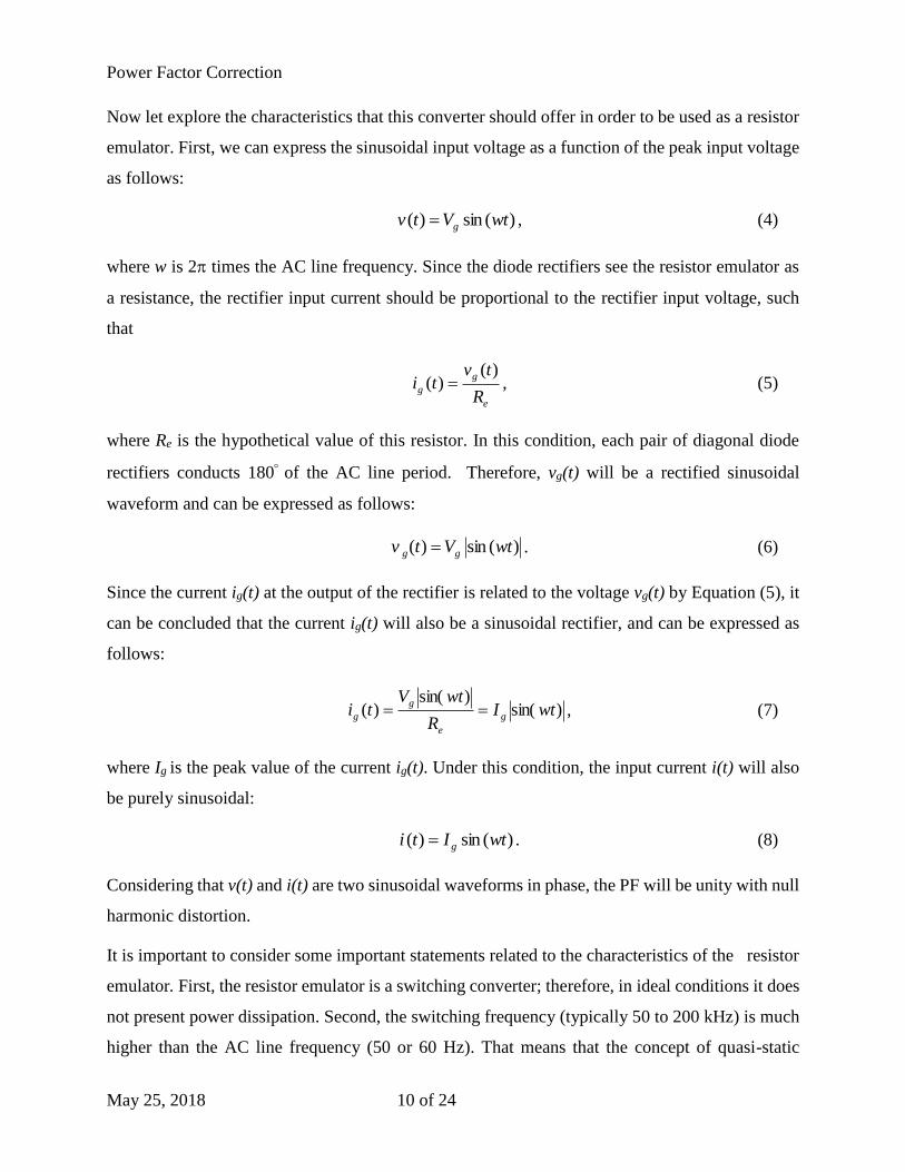
Active solutions are a more suitable option for improving PF and harmonic distortion in higher-
power applications. In these active solutions, a converter with switching frequencies higher than
the AC line frequency is placed between the output of the diode rectifiers and the bulk capacitor,
as shown in Figure 5. The reactive elements of this converter are small, because the size depends
on the converter switching frequency rather than the AC line frequency. The function of this
converter is to behave as an ideal resistive load for the output of the diode rectifiers in order to
eliminate the generation of line current harmonics. Due to this characteristic, the converter is also
known as a resistor emulator.
Figure 5. Circuit diagram of an active power factor correction scheme.
Co
Mains
Inputs
Lo
Ci
Co
Mains
Inputs
Lo
Ci
v(t)
i(t)THD =29%v(t)
i(t)THD =29%
C
Dc to DC
Converter(Resistor Emulator)
iOdc(t)iO(t)
+
ig(t)
+
-
vg(t)
+
-
vo(t)
iOac(t)i(t)
v(t)+
- C
Dc to DC
Converter(Resistor Emulator)
Dc to DC
Converter(Resistor Emulator)
iOdc(t)iO(t)
+
ig(t)
+
-
vg(t)
+
-
vo(t)
iOac(t)i(t)
v(t)+
-
Power Factor Correction
May 25, 2018 10 of 24
Now let explore the characteristics that this converter should offer in order to be used as a resistor
emulator. First, we can express the sinusoidal input voltage as a function of the peak input voltage
as follows:
)(sin)( twVtv g , (4)
where w is 2 times the AC line frequency. Since the diode rectifiers see the resistor emulator as
a resistance, the rectifier input current should be proportional to the rectifier input voltage, such
that
e
g
gR
tvti
)()( , (5)
where Re is the hypothetical value of this resistor. In this condition, each pair of diagonal diode
rectifiers conducts 180 of the AC line period. Therefore, vg(t) will be a rectified sinusoidal
waveform and can be expressed as follows:
)(sin)( twVtv gg . (6)
Since the current ig(t) at the output of the rectifier is related to the voltage vg(t) by Equation (5), it
can be concluded that the current ig(t) will also be a sinusoidal rectifier, and can be expressed as
follows:
)sin()sin(
)( twIR
twVti g
e
g
g , (7)
where Ig is the peak value of the current ig(t). Under this condition, the input current i(t) will also
be purely sinusoidal:
)(sin)( twIti g . (8)
Considering that v(t) and i(t) are two sinusoidal waveforms in phase, the PF will be unity with null
harmonic distortion.
It is important to consider some important statements related to the characteristics of the resistor
emulator. First, the resistor emulator is a switching converter; therefore, in ideal conditions it does
not present power dissipation. Second, the switching frequency (typically 50 to 200 kHz) is much
higher than the AC line frequency (50 or 60 Hz). That means that the concept of quasi-static
Power Factor Correction
May 25, 2018 11 of 24
conditions can be applied for the analysis of the converter. This concept considers that the input
voltage does not change during a switching cycle of the resistor emulator.
In addition, as mentioned before, the reactive elements are selected according to the switching
frequency. Therefore, they can only store energy during a switching cycle and not during a long
period of time as this one presented during a line cycle.
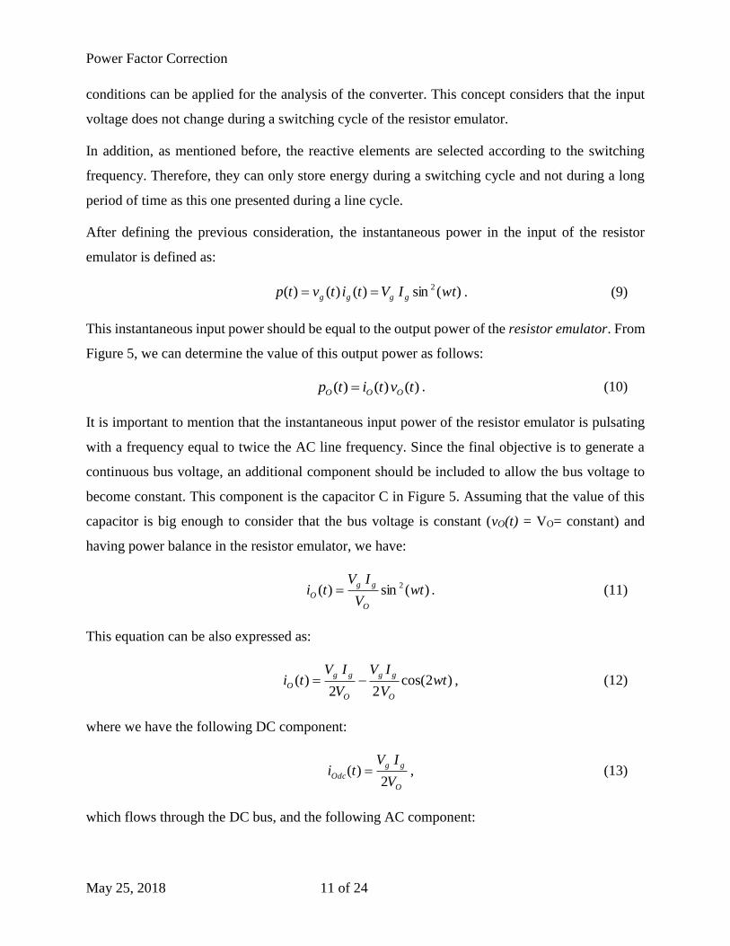
After defining the previous consideration, the instantaneous power in the input of the resistor
emulator is defined as:
)(sin)()()( 2 wtIVtitvtp gggg . (9)
This instantaneous input power should be equal to the output power of the resistor emulator. From
Figure 5, we can determine the value of this output power as follows:
)()()( tvtitp OOO . (10)
It is important to mention that the instantaneous input power of the resistor emulator is pulsating
with a frequency equal to twice the AC line frequency. Since the final objective is to generate a
continuous bus voltage, an additional component should be included to allow the bus voltage to
become constant. This component is the capacitor C in Figure 5. Assuming that the value of this
capacitor is big enough to consider that the bus voltage is constant (vO(t) = VO= constant) and
having power balance in the resistor emulator, we have:
)(sin)( 2 twV
IVti
O
gg
O . (11)
This equation can be also expressed as:
)2cos(22
)( twV
IV
V
IVti
O
gg
O
gg
O , (12)
where we have the following DC component:
O
gg
OdcV
IVti
2)( , (13)
which flows through the DC bus, and the following AC component:
Power Factor Correction
May 25, 2018 12 of 24
)2cos(2
)( twV
IVti
O
gg
Odc , (14)
which flows entirely through the capacitor C considering that the value of this capacitor was well
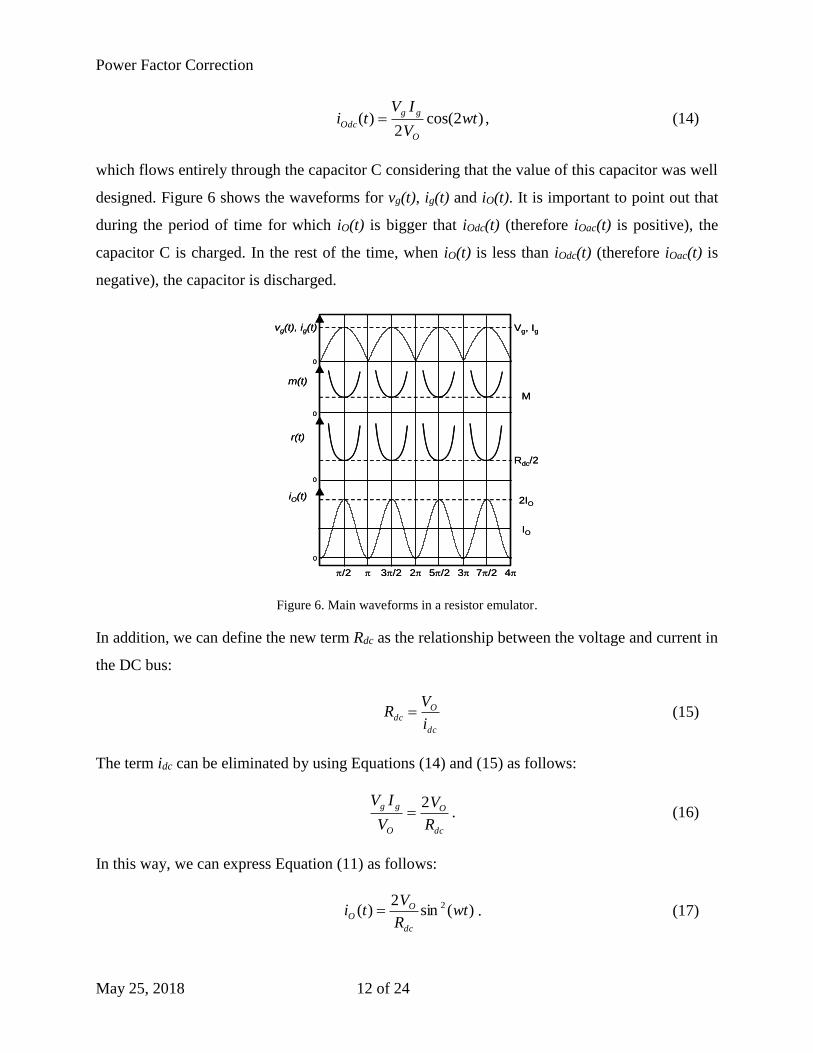
designed. Figure 6 shows the waveforms for vg(t), ig(t) and iO(t). It is important to point out that
during the period of time for which iO(t) is bigger that iOdc(t) (therefore iOac(t) is positive), the
capacitor C is charged. In the rest of the time, when iO(t) is less than iOdc(t) (therefore iOac(t) is
negative), the capacitor is discharged.
Figure 6. Main waveforms in a resistor emulator.
In addition, we can define the new term Rdc as the relationship between the voltage and current in
the DC bus:
dc
Odc
i
VR (15)
The term idc can be eliminated by using Equations (14) and (15) as follows:
dc
O
O
gg
R
V
V
IV 2 . (16)
In this way, we can express Equation (11) as follows:
)(sin2
)( 2 twR
Vti
dc
OO . (17)
/2 3/2 2 5/2 3 7/2 4
IO
2IO
Rdc/2
M
Vg, Ig
r(t)
m(t)
vg(t), ig(t)
iO(t)
0
0
0
0
/2 3/2 2 5/2 3 7/2 4
IO
2IO
Rdc/2
M
Vg, Ig
r(t)
m(t)
vg(t), ig(t)
iO(t)
0
0
0
0
Power Factor Correction
May 25, 2018 13 of 24
Now, if we define the resistor seen by the resistor emulator, r(t) as the relationship between the
voltage VO in the output and the current iO(t), we obtain the following expression:
)(sin2)(
)(2 wt
R
ti
Vtr dc
O
O . (18)
From this equation we can make the first important statement related to the characteristics of the
resistor emulator: It sees at the output a load resistor, which is different from the load resistor seen
by the DC bus. Both load resistors are related by Equation (18); in this way the resistor emulator
sees wide variations of load, with a range between Rdc/2 to an infinite value.
On the other hand, there is another important characteristic that should be present in the resistor
emulator. By considering the converter conversion ratio, m(t) defined by the relationship between
the constant output voltage VO and vg(t), and using Equation (6), we can define the following
expression:
)sin()(
)(wt
M
tv
Vtm
g
O , (19)
where M=VO/Vg is the relationship between the output voltage and the peak value of the AC line
waveform. From Equation (19) we can state that the conversion ratio for a resistor emulator varies
between infinity (at the AC line voltage zero crossing) and some minimum value M (at the peak
of the AC line voltage waveforms).
Equations (18) and (19) are very important for defining the operating characteristics of a resistor
emulator, and thus to select the DC/DC converter that can meet these requirements. Several pulse
width modulation (PWM) topologies for DC/DC converters can be used as resistor emulators in a
PF system. However, we will focus on the boost topology since it is the most popular
implementation for medium- and high-power applications.
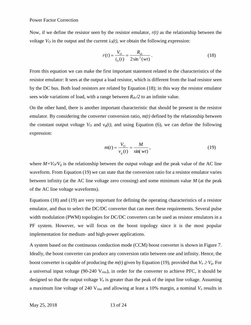
A system based on the continuous conduction mode (CCM) boost converter is shown in Figure 7.
Ideally, the boost converter can produce any conversion ratio between one and infinity. Hence, the
boost converter is capable of producing the m(t) given by Equation (19), provided that Vo Vg. For
a universal input voltage (90-240 Vrms), in order for the converter to achieve PFC, it should be
designed so that the output voltage Vo is greater than the peak of the input line voltage. Assuming
a maximum line voltage of 240 Vrms and allowing at least a 10% margin, a nominal Vo results in
Power Factor Correction
May 25, 2018 14 of 24
380 V. The relative high output voltage is actually an advantage for the step-down converter
following the CCM boost converter. The current levels in the silicon and transformer of the step-
down converter are moderate, resulting in lower-cost devices. Another characteristic of the boost
converter is that it can produce very low THD, with better transistor utilization than other
approaches; the efficiency of the active boost circuit is very high, approaching 95%.
Figure 7. Rectifier system based on the boost converter using a multiplier controller.
The CCM boost converter needs two control loops to control both the input current and the output
voltage. One of the control loops, the input current loop, commands the DC/DC converter to work
as a half-sinusoidal current sink at its input. The other control loop, the output voltage loop,
commands the DC/DC converter to work as a DC voltage source at its output. This kind of
controller is typically called a multiplier controller. The basic simplified multiplier controller can
be also seen in Figure 7. As shown, there is a feedback current loop that forces the pulse modulation
of switch S in such a way that the input current follows the reference iref(t). An analog multiplier
creates iref(t) by multiplying the rectified line voltage by the output of the voltage of the error
amplifier ve(t). Thus, the input current is a rectified sinusoidal, the value of which depends on ve(t).
In this way, ve(t) controls the power drawn from the utility line, and considering that the resistor
emulator (in this case the boost converter) is a non-dissipative element, it also controls the power
delivered to the load. It is equivalent to say that for every load, ve(t) determines the voltage that is
applied to the load. Therefore, using a feedback loop of the output voltage whose output will be
the error signal ve(t), the output voltage becomes perfectly constant.
CB
Bulk
capacitor
C
Rdc+
-
+
-
Multiplier
ig(t)
+
-
Vg(t)
+
-
Vo(t)S
DL
Boost converter
v(t)
iO(t)
i(t)
+
-
X
PWM
+-
Low pass
filter-+ Gc(s)
Rs
Compensator
ig(t)
Vg(t)
Vref
Controller
iref(t) ve(t)
CB
Bulk
capacitor
C
Rdc+
-
+
-
Multiplier
ig(t)
+
-
Vg(t)
+
-
Vo(t)S
DL
Boost converter
v(t)
iO(t)
i(t)
+
-
XX
PWMPWM
+-+-
Low pass
filter
Low pass
filter-+
-+ Gc(s)Gc(s)
RsRs
Compensator
ig(t)
Vg(t)
Vref
Controller
iref(t) ve(t)
Power Factor Correction
May 25, 2018 15 of 24
It is important to point out that ve(t) must be constant; otherwise, the rectified input current would
not be a rectified sinusoidal and neither would the utility line current. In order to meet the
requirement for ve(t), a low-pass filter must be used to eliminate the ripple in the output voltage.
This low-pass filter results in a slow feedback loop.
On the other hand, the current feedback loop should be as fast as possible to guarantee that the
input current follows the reference iref(t). For the implementation of the current feedback loop,
either peak current mode control or average current mode control may be used. In the peak current
mode control approach, the peak current of the inductor is used to force the input current to follow
the reference. Despite the simplicity of controlling the input current, this approach presents a low-
gain, wide-bandwidth current loop, which generally makes it unsuitable for a high-performance
PF corrector, since there is a significant error between the reference and the current. This error will
produce distortion and a poor PF.
The conceptual diagram of a CCM boost converter using average current mode control is also
shown in Figure 7. This approach is based on a simple concept. The amplifier Gc(s) is used in the
feedback loop to average the inductor current. Therefore, the average inductor current is used
instead of the peak current to track the reference iref(t) with very little error. Another important
feature of the average current mode control is that near the zero crossings of the line voltage, the
converter operates with the maximum duty cycle. As a result, the dead angle period, which is
present in the peak current mode control, is reduced. Average current mode control is relatively
easy to implement. As a result, it is the method used for the implementation of the active PFC in
this experiment.
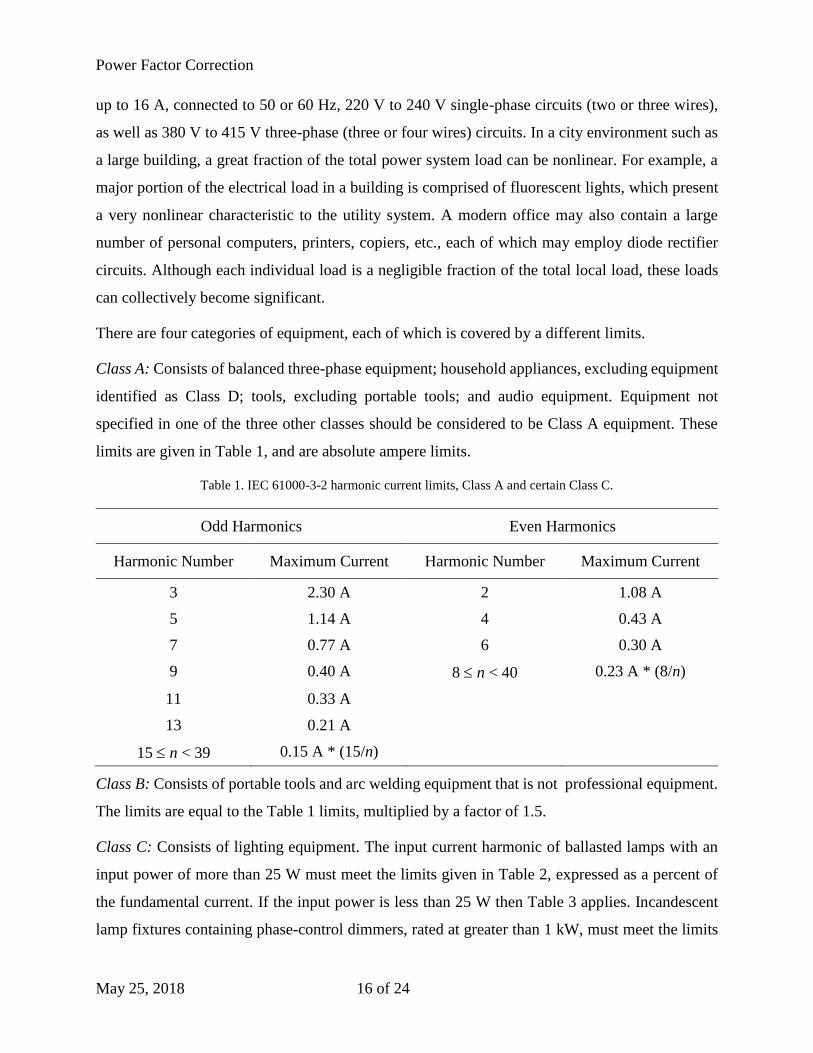
AC LINE CURRENT HARMONIC STANDARD
International Electrotechnical Commission Standard IEC 61000-3-2
The standard that forms the foundation for both present and proposed future harmonic current
standards is the IEC 555 (now the IEC 61000-3-2). The IEC 555 was first released in draft form
in 1982, has since received a number of revisions, and is presently considered the de facto
worldwide harmonic current emission standard for commercial equipment.
The IEC 61000-3-2 standard covers a number of different types of low-power equipment, with
varied harmonic limits. It specifically limits harmonics for equipment having an input current of
Power Factor Correction
May 25, 2018 16 of 24
up to 16 A, connected to 50 or 60 Hz, 220 V to 240 V single-phase circuits (two or three wires),
as well as 380 V to 415 V three-phase (three or four wires) circuits. In a city environment such as
a large building, a great fraction of the total power system load can be nonlinear. For example, a
major portion of the electrical load in a building is comprised of fluorescent lights, which present
a very nonlinear characteristic to the utility system. A modern office may also contain a large
number of personal computers, printers, copiers, etc., each of which may employ diode rectifier
circuits. Although each individual load is a negligible fraction of the total local load, these loads
can collectively become significant.
There are four categories of equipment, each of which is covered by a different limits.
Class A: Consists of balanced three-phase equipment; household appliances, excluding equipment
identified as Class D; tools, excluding portable tools; and audio equipment. Equipment not
specified in one of the three other classes should be considered to be Class A equipment. These
limits are given in Table 1, and are absolute ampere limits.
Table 1. IEC 61000-3-2 harmonic current limits, Class A and certain Class C.
Odd Harmonics Even Harmonics
Harmonic Number Maximum Current Harmonic Number Maximum Current
3 2.30 A 2 1.08 A
5 1.14 A 4 0.43 A
7 0.77 A 6 0.30 A
9 0.40 A 8 n < 40 0.23 A * (8/n)
11 0.33 A
13 0.21 A
15 n < 39 0.15 A * (15/n)
Class B: Consists of portable tools and arc welding equipment that is not professional equipment.
The limits are equal to the Table 1 limits, multiplied by a factor of 1.5.
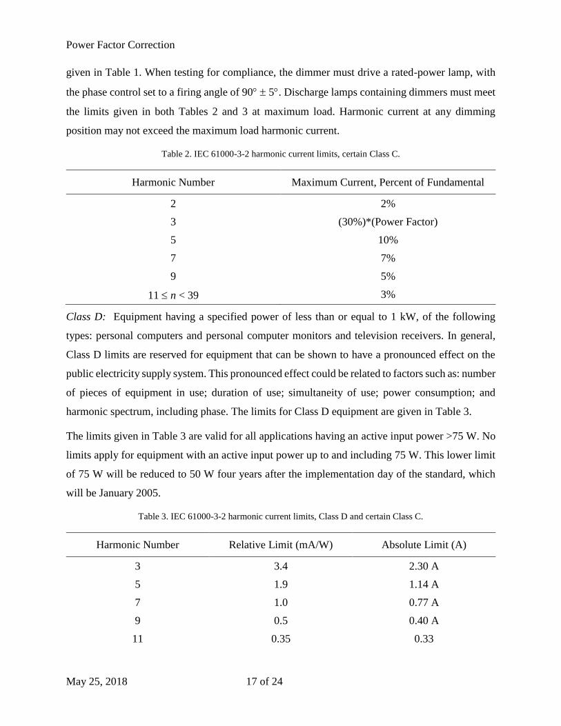
Class C: Consists of lighting equipment. The input current harmonic of ballasted lamps with an
input power of more than 25 W must meet the limits given in Table 2, expressed as a percent of
the fundamental current. If the input power is less than 25 W then Table 3 applies. Incandescent
lamp fixtures containing phase-control dimmers, rated at greater than 1 kW, must meet the limits
Power Factor Correction
May 25, 2018 17 of 24
given in Table 1. When testing for compliance, the dimmer must drive a rated-power lamp, with
the phase control set to a firing angle of 90 5. Discharge lamps containing dimmers must meet
the limits given in both Tables 2 and 3 at maximum load. Harmonic current at any dimming
position may not exceed the maximum load harmonic current.
Table 2. IEC 61000-3-2 harmonic current limits, certain Class C.
Harmonic Number Maximum Current, Percent of Fundamental
2 2%
3 (30%)*(Power Factor)
5 10%
7 7%
9 5%
11 n < 39 3%
Class D: Equipment having a specified power of less than or equal to 1 kW, of the following
types: personal computers and personal computer monitors and television receivers. In general,
Class D limits are reserved for equipment that can be shown to have a pronounced effect on the
public electricity supply system. This pronounced effect could be related to factors such as: number
of pieces of equipment in use; duration of use; simultaneity of use; power consumption; and
harmonic spectrum, including phase. The limits for Class D equipment are given in Table 3.
The limits given in Table 3 are valid for all applications having an active input power >75 W. No
limits apply for equipment with an active input power up to and including 75 W. This lower limit
of 75 W will be reduced to 50 W four years after the implementation day of the standard, which
will be January 2005.
Table 3. IEC 61000-3-2 harmonic current limits, Class D and certain Class C.
Harmonic Number Relative Limit (mA/W) Absolute Limit (A)
3 3.4 2.30 A
5 1.9 1.14 A
7 1.0 0.77 A
9 0.5 0.40 A
11 0.35 0.33
Power Factor Correction
May 25, 2018 18 of 24
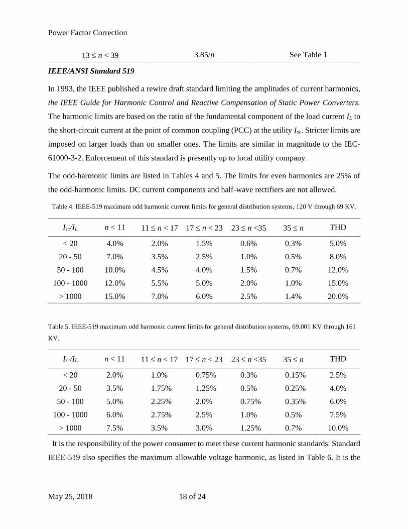
13 n < 39 3.85/n See Table 1
IEEE/ANSI Standard 519
In 1993, the IEEE published a rewire draft standard limiting the amplitudes of current harmonics,
the IEEE Guide for Harmonic Control and Reactive Compensation of Static Power Converters.
The harmonic limits are based on the ratio of the fundamental component of the load current IL to
the short-circuit current at the point of common coupling (PCC) at the utility Isc. Stricter limits are
imposed on larger loads than on smaller ones. The limits are similar in magnitude to the IEC-
61000-3-2. Enforcement of this standard is presently up to local utility company.
The odd-harmonic limits are listed in Tables 4 and 5. The limits for even harmonics are 25% of
the odd-harmonic limits. DC current components and half-wave rectifiers are not allowed.
Table 4. IEEE-519 maximum odd harmonic current limits for general distribution systems, 120 V through 69 KV.
Isc/IL n < 11 11 n < 17 17 n < 23 23 n <35 35 n THD
< 20 4.0% 2.0% 1.5% 0.6% 0.3% 5.0%
20 - 50 7.0% 3.5% 2.5% 1.0% 0.5% 8.0%
50 - 100 10.0% 4.5% 4.0% 1.5% 0.7% 12.0%
100 - 1000 12.0% 5.5% 5.0% 2.0% 1.0% 15.0%
> 1000 15.0% 7.0% 6.0% 2.5% 1.4% 20.0%
Table 5. IEEE-519 maximum odd harmonic current limits for general distribution systems, 69.001 KV through 161
KV.
Isc/IL n < 11 11 n < 17 17 n < 23 23 n <35 35 n THD
< 20 2.0% 1.0% 0.75% 0.3% 0.15% 2.5%
20 - 50 3.5% 1.75% 1.25% 0.5% 0.25% 4.0%
50 - 100 5.0% 2.25% 2.0% 0.75% 0.35% 6.0%
100 - 1000 6.0% 2.75% 2.5% 1.0% 0.5% 7.5%
> 1000 7.5% 3.5% 3.0% 1.25% 0.7% 10.0%
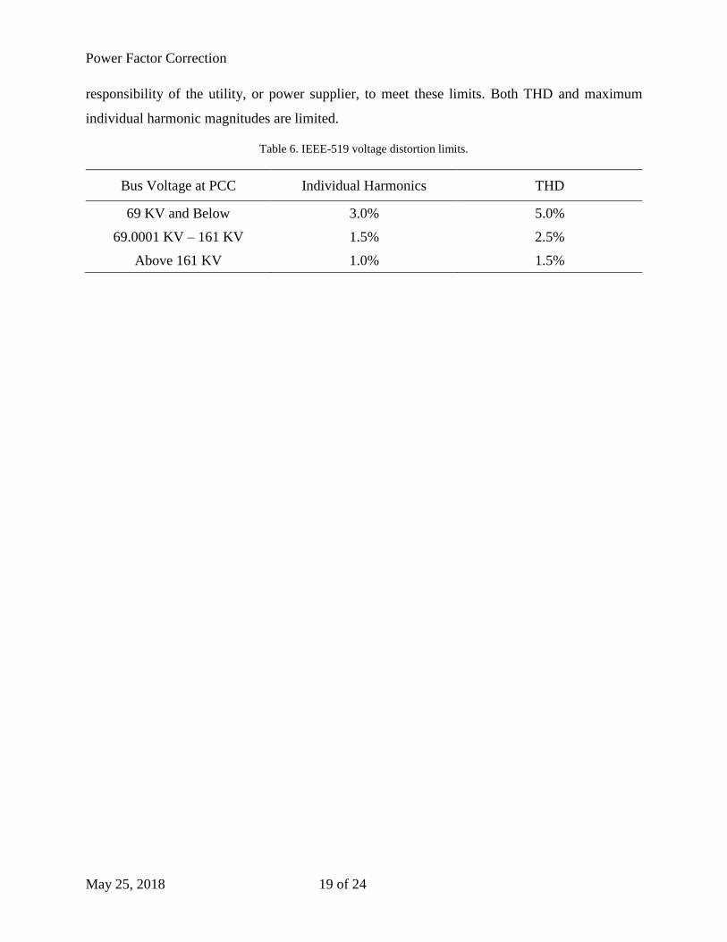
It is the responsibility of the power consumer to meet these current harmonic standards. Standard
IEEE-519 also specifies the maximum allowable voltage harmonic, as listed in Table 6. It is the
Power Factor Correction
May 25, 2018 19 of 24
responsibility of the utility, or power supplier, to meet these limits. Both THD and maximum
individual harmonic magnitudes are limited.
Table 6. IEEE-519 voltage distortion limits.
Bus Voltage at PCC Individual Harmonics THD
69 KV and Below 3.0% 5.0%
69.0001 KV – 161 KV 1.5% 2.5%
Above 161 KV 1.0% 1.5%
Power Factor Correction
May 25, 2018 20 of 24
W A R N I N G
Since you will be working with circuits with potentially lethal levels of input and output voltages,
you are required to exercise extreme caution to avoid any accidents. Do not touch any part of the
circuits (power stage or control) when the circuits are connected to the AC sources and are up and
running. Also, be extremely careful when connecting measuring equipment to the circuit. Make
all the necessary connections when the AC source is turned off. If you are not sure or you do not
know how to use or connect any piece of the equipment, please call a lab instructor. Finally, you
are required to wear safety glasses (provided) when running the circuits.
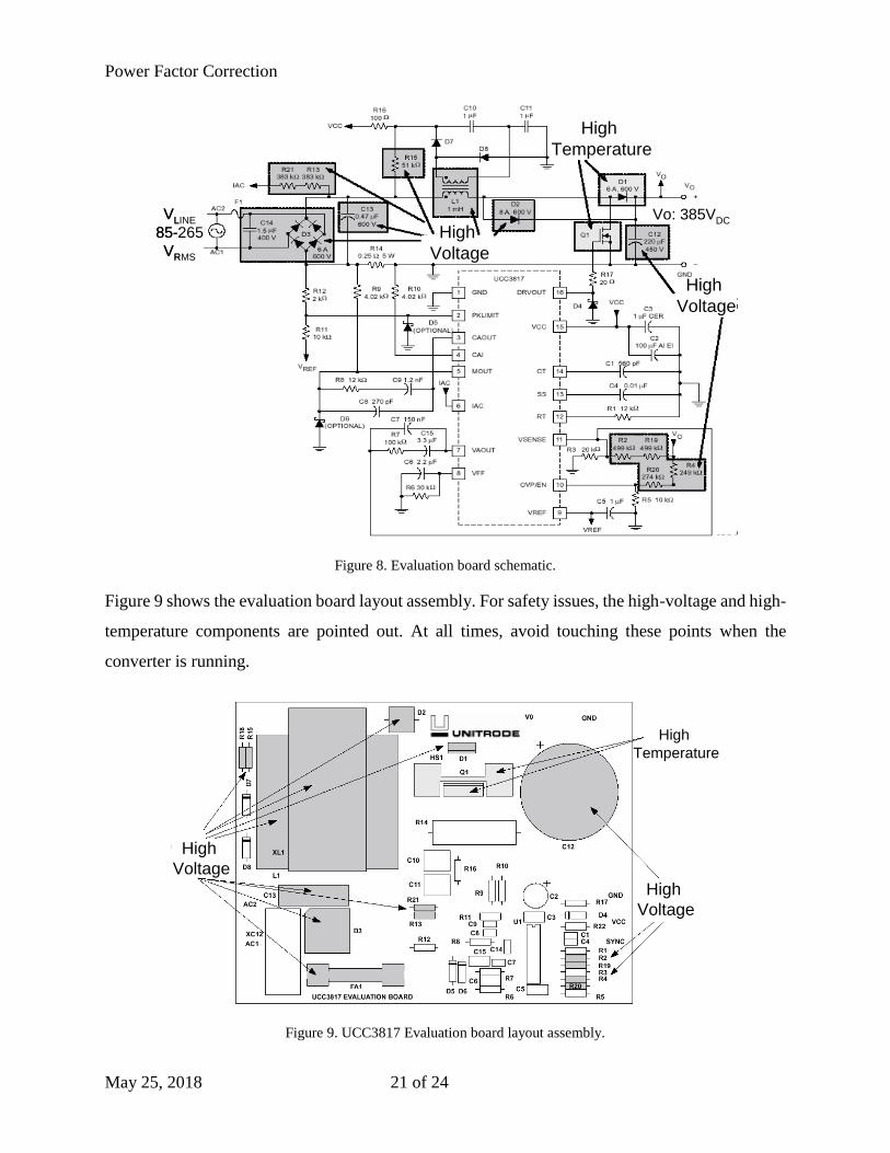
SUGGESTED PROCEDURE
For the realization of this experiment, you are going to use the UCC3817 BiCMOS PF preregulator
evaluation board from Texas Instruments. The board schematic is shown in Figure 8. As can be
seen, the PF preregulator is based on a CCM boost converter. The main features in the evaluation
board are listed as follows:
Designed to comply with IEC 61000-3-2
Worldwide line operation RMS voltage range from 85 V to 265 V
Regulated 385V, 250W (max) DC output
Accurate power limiting
Accurate overvoltage protection
The multiplier controller is implemented with the UCC3817 IC chip from Texas Instruments,
which simplified the complexity of the control requirements. The controller achieves near-unity
PF by shaping the AC input line current waveforms to correspond to that of the AC input line
voltage. Average current mode control maintains stable, low-distortion, sinusoidal line current.
Power Factor Correction
May 25, 2018 21 of 24
Figure 8. Evaluation board schematic.
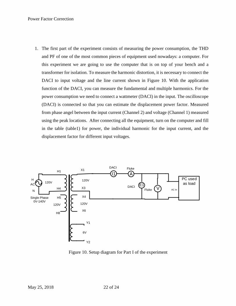
Figure 9 shows the evaluation board layout assembly. For safety issues, the high-voltage and high-
temperature components are pointed out. At all times, avoid touching these points when the