23
BUCK CIRCUIT DESIGN Done BY : Mohammed Ahmed Mohammed Ahmed Student ID : TP018711 Intake Code : UC4f1404ME Individual Assignment
| Date post: | 27-Dec-2015 |
| Category: |
Documents |
| Upload: | ahmed-asnag |
| View: | 78 times |
| Download: | 1 times |
Buck Circuit Design
Intake Code : UC4f1404ME
Individual Assignment

Page 1 of 19

1.0 Introduction:
In many industrial applications, it is required to convert a fixed voltage dc source into a
variable voltage dc source. Hence , the switch dc to dc converter is used. A dc-dc converter
can be considered as an equivalent to an Ac transformer with continuously variable turn ratio.
Like a transformer, it could be used to step-up or step-down a dc voltage source. Dc to dc
converters are widely used for traction motor control in automobiles, trolley cars, marine
hoists, forklift trucks and mine haulers. They provide a smooth acceleration control, high
efficiency and fast dynamic response. Dc to dc converters can be used as a regenerative
braking of dc motors to return energy back into the supply. It also used in dc voltage
regulator since it is the major interested utilization where it is available in almost every
electronics device , motherboards , mobile phones , internet modems , etc.
As a dc voltage regulator. Switching dc-dc converters considered efficient alternatives to the
linear regulator. In a switching dc-dc converter circuit, the transistor operates as an electronic
switch by being completely on or completely off (saturation or cut-off for a BJT or the triode
and cut-off regions of a MOSFET). This circuit is also known as a dc chopper.
Historically, DC/DC converters were often designed by the product design engineer out of
discrete components, but as technology has moved on and the requirements for faster
development and improved time to market dominate, converter design is being left more and
more in the hands of specialist manufacturers. The DC/DC converter is one of the most
critical components in any design and the choice of converter can have a dramatic effect on
the quality of the final product. Ideally power architecture design should be undertaken at the
start of any design to help remove the costs associated with interference, oscillations,
overheating and overcurrent as well as improving reliability and speeding up the design of the
system.
Page 2 of 19

2.0 Theory of operation and applications:
2.1 Theory of operation :
Buck circuit is a dc to dc converter circuit it used to step down the input
voltage to a desired level. As it shown in fig(1) the buck circuit consist of
DC input voltage source (Vs) , a transistor switch , diode (D) , filter
inductor (L) , Filter capacitor (C) and an output load (R).
Figure1 (Buck converter circuit)
(Source : http://www.learnabout-electronics.org/PSU/psu31.php )
The buck circuit operates in two oscillatory states which are; the switch ON state and the
switch OFF state. Both of the switch on and the switch off status are occurred by driving
pulse signal into the switching transistor gate (MOSFET) or base (BJT).
Switch ‘on’ State:
When the pulse signal turns high (assuming the switch to be N-channel MOSFET transistor)
the transistor will be forward biased which enable the current to flow to the load. Initially
current flow to the load is restricted as energy is also being stored in the inductor L1 in a
magnetic field form, therefore the current in the load and the charge on the capacitor C1
Page 3 of 19

builds up gradually during the ‘on’ state. Throughout the ‘on’ state, there will be a large
positive voltage on D1 cathode and so the diode will be reverse biased and therefore it will
act as an open circuit (see Fig(2)).
Figure 2 (Buck converter in ‘On’ state)
(Source : http://www.learnabout-electronics.org/PSU/psu31.php )
Switch ‘Off’ State:
When the pulse signal turns low (0V) as it seen in fig (3) , the energy stored in the magnetic
field around the inductor L1 is collapsed and turned back -induced- into the circuit as a e.m.f
(electromotive force) . The e.m.f voltage across the inductor will be in reverse polarity to the
voltage across L1 during the ‘on’ state, and the stored energy which is available in the
collapsing magnetic field is sufficient to keep current flowing for at minimum the time
which the transistor will be switched open.The back e.m.f. from the inductor now causes
current to flow around the circuit via the load R and the diode D1, which is forward biased in
the switch off state . Once the inductor has returned a large part of its stored energy to the
circuit and the load voltage begins to fall, the charge stored in C1 becomes the main source of
current, keeping current flowing through the load until the next ‘on’ state begins.
Page 4 of 19
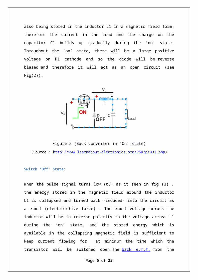
Figure 3(Buck converter in ‘Off’ state)
(Source : http://www.learnabout-electronics.org/PSU/psu31.php )
The overall effect of this is that, instead of a large square wave appearing across the load,
there remains only a ripple waveform, i.e. small amplitude, high frequency triangular wave
with a required DC level.
2.2 Applications:
There are a huge uncounted list of various applications of the buck converter , and few is
mentioned below :
1- Dc motor controlling.
2- To supply the core in GPUs in mobile applications.
3- Available in almost any motherboards.
3.0 Design principle:
During the designing and the analysis of a buck circuit there are some steps needed to be
considered and assumptions to be made .
Page 5 of 19

3.1 The assumptions:
1. The circuit is operating in the steady state.
2. The inductor current is continuous (always positive).
3. The capacitor is very large, and the output voltage is held constant at voltage Vo. This
restriction will be relaxed later to show the effects of finite capacitance.
4. The switching period is T; the switch is closed for time DT and open for time (1_D)T.
5. The components are ideal.
Note :
The key to the analysis for determining the output Vo is to examine the inductor current and
inductor voltage first for the switch closed and then for the switch open. The net change in
inductor current over one period must be zero for steady state operation. The average
inductor voltage is zero.
3.2 The steps:
1-Determination of converter specifications
By collecting whatever information possibly pre-given or important for the circuit to meet
some specifications such as input voltage , output voltage , voltage ripple , current ripple or
even switching frequency. And most importantly, circuit efficiency needed to be considered.
2- Inductor selection :
Calculating the inductor value is most critical in designing a step-down switching converter.
First, assume the converter is in continuous-current mode(CCM), which is usually the case.
CCM implies that the inductor does not fully discharge during the switch-off time. The
following equations assume an ideal switch (zero on resistance, infinite off-resistance and
zero switching time) and an ideal diode
Lmin =(1-D)RL/2ƒ
Maximum current through the inductor determines the inductor’s required saturation-current
rating, which in turn dictates the approximate size of the inductor. Saturating the inductor
core decreases the converter efficiency, while increasing the temperatures of the inductor, the
Page 6 of 19

MOSFET and the diode. You can calculate the inductor’s maximum operating current as
follows:
Imax = iL + Δίl/2
Also minimum current produced by the inductor can be calculated by :
Imin = ίL – Δίl/2
3-Capacitor section :
Output capacitance is required to minimize the voltage overshoot and ripple present at the
output of a step-down converter. Large overshoots are caused by insufficient output
capacitance, and large voltage ripple is caused by insufficient capacitance as well as a high
equivalent-series resistance (ESR) in the output capacitor. The maximum allowed output-
voltage overshoot and ripple are usually specified at the time of design. Thus, to meet the
ripple specification for a step-down converter circuit, you must include an output capacitor
with ample capacitance and low ESR.The problem of overshoot, in which the output-voltage
overshoots its regulated value when a full load is suddenly removed from the output, requires
that the output capacitor be large enough to prevent stored inductor energy from launching
the output above the specified maximum output voltage. The capacitor value can be
calculated using the following equation:
C = (1-D)/(8L× ΔVo/Vo × ƒ^2)
4.0 Analytic calculation :
Given :
Vs = 48V
Vo = 18V
RL = 10Ω
Then :
Page 7 of 19

D = Vs/Vo
D = 18/48
D = 0.375
Let ƒ = 50 KHz
-Inductor Value :
Lmin =(1-D)RL/2ƒ
Lmin = (1-0.375) ×10 /(2×50×1000)
Lmin = 62.5 μh
To insure that the inductor current is continuous , the inductor size shall be 30% larger than
the minimum inductor size .
Thus ,
L = Lmin ×1.3
L = 62.5 μh × 1.3
L= 81.25 μh
-Average inductor current (Δίl) :
Δίl = ( Vs-Vo )DT/L
Δίl = ((48-18)× 0.375) / (81.25×10^-6 × 50 ×10^3)
Δίl = 2.77 A
iL = Vo/R
iL = 18/10
iL = 1.8 A
-Imax and Imin :
Page 8 of 19

Imax = iL + Δίl/2
Imax = 1.8 + (2.77/2)
Imax = 3.19 A
Imin = ίL – Δίl/2
Imin = 1.8 – (2.77/2)
Imin = 0.42 A
-Capacitance:
C = (1-D)/(8L× ΔVo/Vo × ƒ^2)
Note : since the output voltage ripple shouldn’t exceed 0.5% then ΔVo/Vo assumed to
be 0.4%.
C = (1-0.375)/(8×81.25 ×10^-6 × 0.004 50000^2)
C = 9.615 × 10^-5
C = 96.15 μf
Page 9 of 19

5.0 Circuit Simulation:
After the calculation of the circuit parameters, the given and computed values of the circuit
components were keyed in into a simulation programme to test the circuit behaviour . The
utilized simulation program was Simulink matlab (fig 4).
Substituted data:
Vd = 48V; Vo = 18V; R = 10hm; δVo/Vo < 5%
D = 0.375 , ƒ = 50 KHz, L= 81.25 μh , C = 96.15 μf
Figure4 (the designed circuit diagram)
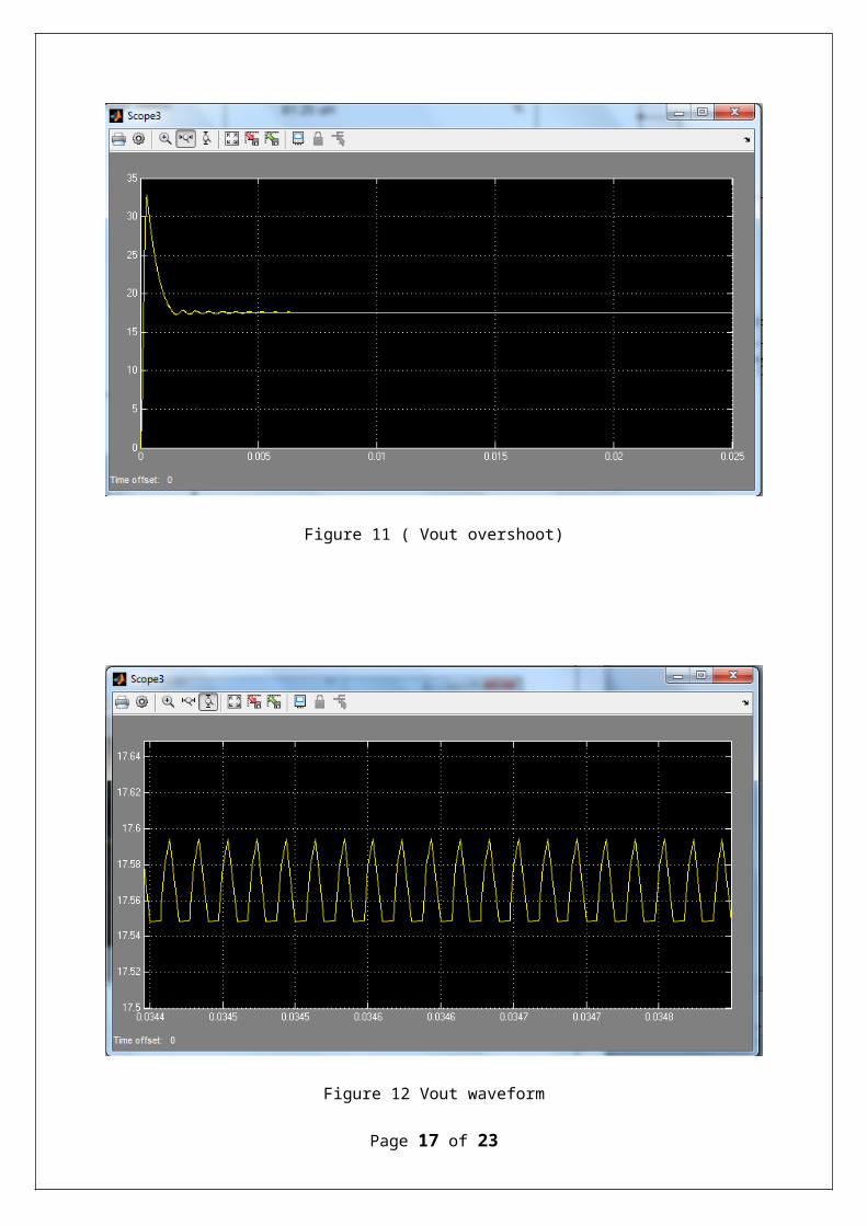
Based on the simulation the Vout is equal to 17.55 V and the current I is equal to 1.755.
Page 10 of 19
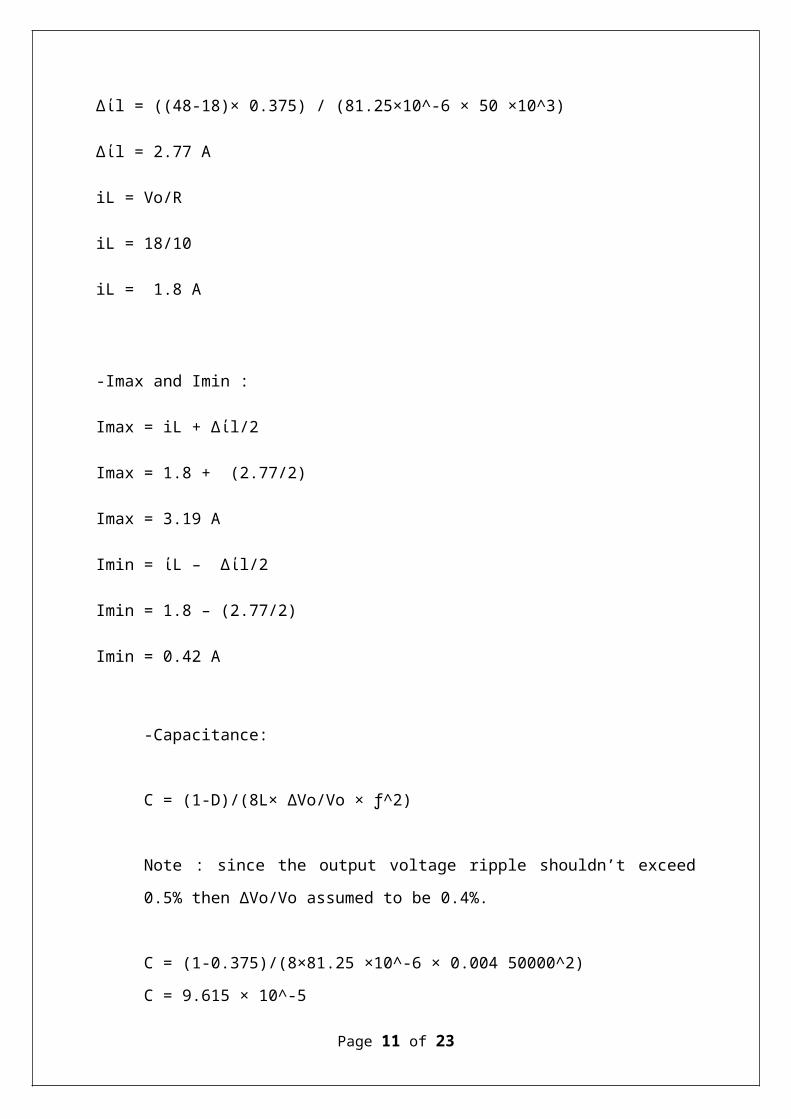
Figure 5 (switching frequency of the switch)
Fig6 (Inductor L voltage signal )
Page 11 of 19

Figure 7( inductor current overshoot)
Figure 8 (inductor current waveform)
Page 12 of 19
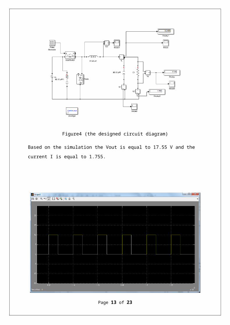
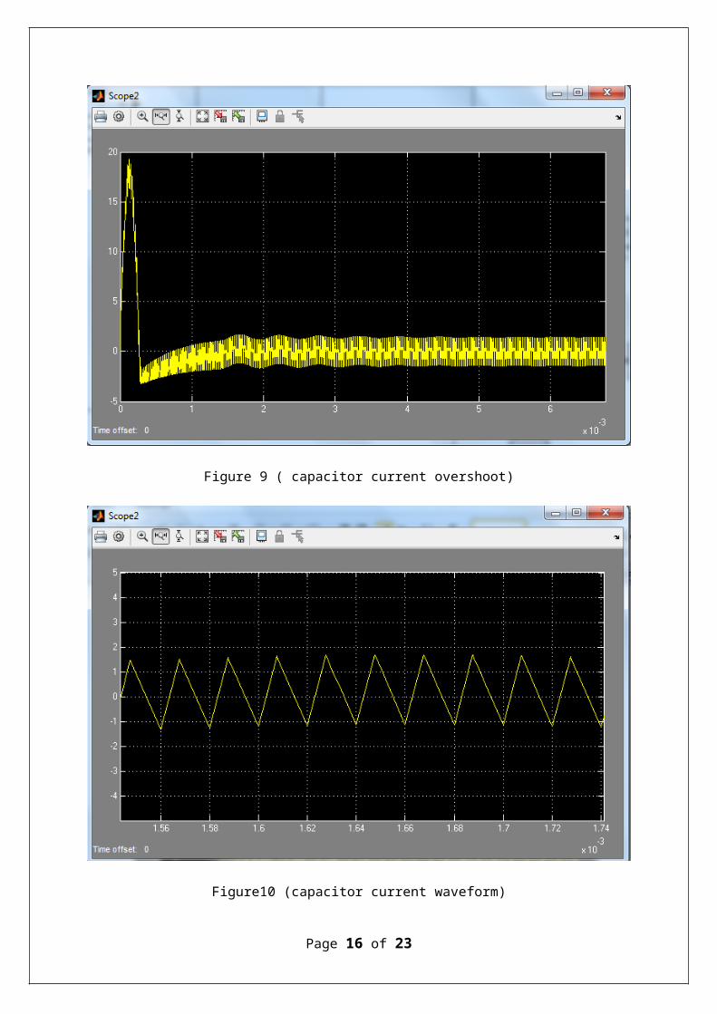
Figure 9 ( capacitor current overshoot)
Figure10 (capacitor current waveform)
Page 13 of 19
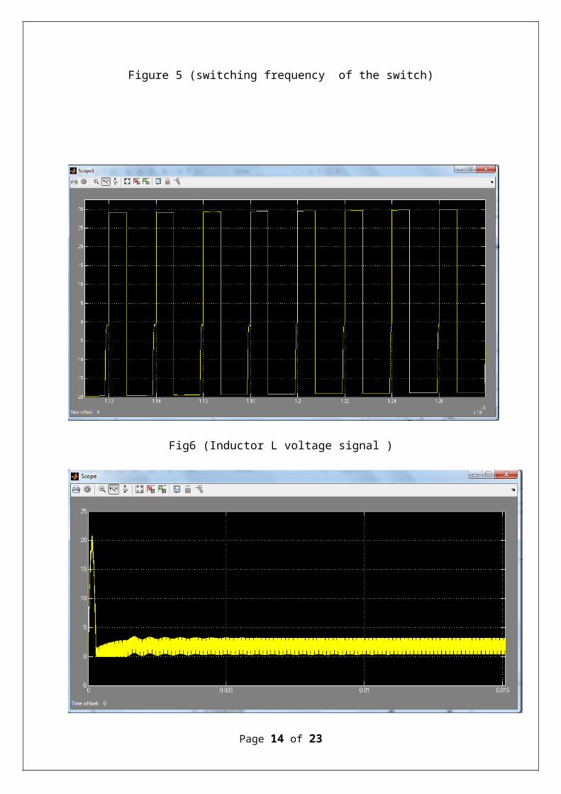
Figure 11 ( Vout overshoot)
Figure 12 Vout waveform
Page 14 of 19
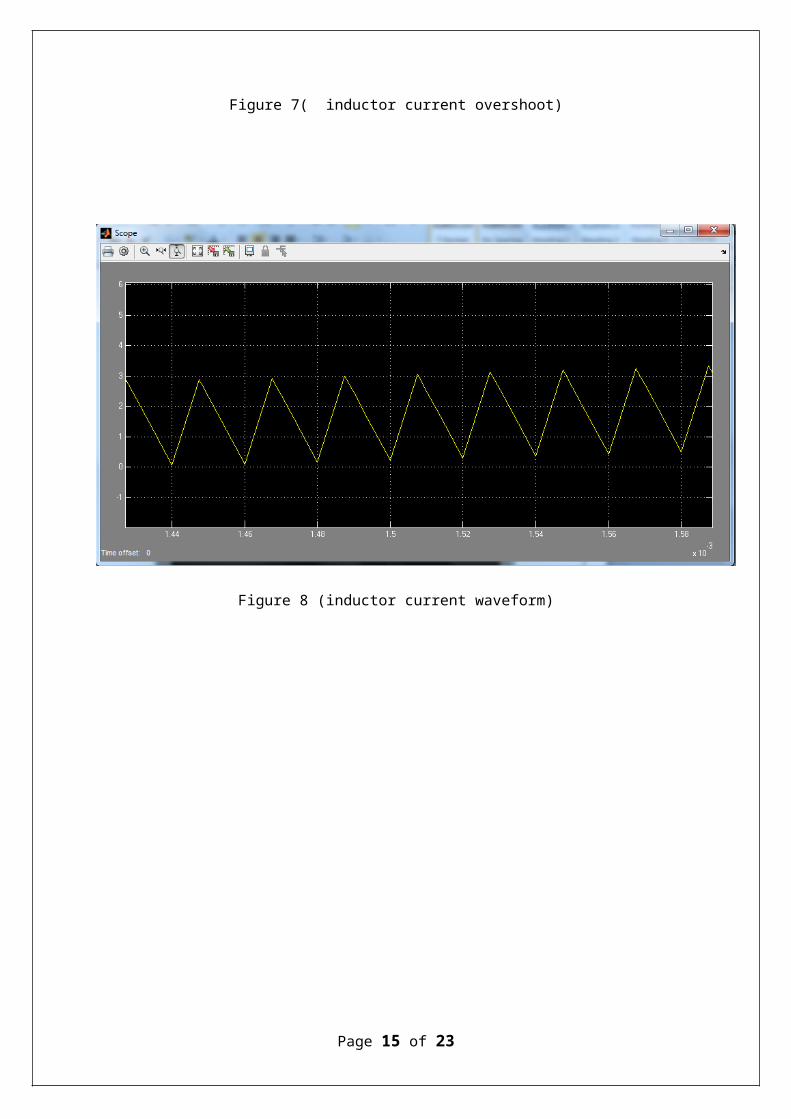
Figure 13( Iout waveform)
Figure14 (circuit simulation 2)
Page 15 of 19
6.0 Discussion :
The simulation result of the designed circuit was quite good , the output voltage is around
17.55 v and meet the standard tolerance which is ±5% according to Microship design
techniques .During the simulation , the values of the capacitor and the inductor was changes
in a try to get a better results .It was realized that when the inductance value was increased
more than initialized calculated value , the inductor current increased and the output voltage
decreased and when the inductor value was lowered less than the calculated value , the
inductor current decreased and the output voltage increased more than it was
needed .therefore, the calculated value of the inductor was suitable enough for the circuit
operation .
When the actual calculated capacitance was increased , the output voltage was increased a bit
but the current was dropped down in a high amount. And vice versa. So basically the
calculated values of the inductor and the capacitor were the most suitable for the circuit
performance.
And since D value play a very important role in the output values of the circuit , it was
obtained that the best d value was D = 38.5 instead of 37.5 , because when this change is
made the vout increased to 18.04V and the current value raised so far till 1.8A. So these
values are the ultimate values for the designed buck converter circuit ( FIG12).The resulted
output voltage drop at the first simulation (Fig4) was due to the diode switching ‘on’ voltage
which is around 0.7 V .To get rid of the overshoot in the circuit output signal , a ceramic
capacitor should be add in parallel with the Voltage source to minimize the input ripple
voltage .
To enhance the circuit as an overall topology, the diode and the switching element should be
chosen carefully based on its datasheet wither it meets the circuit requrment or not ,For
example, choosing a schttoky diode instead of multipurpose one .Moreover , instead of
using the simple buck circuit, synchronous buck circuit type should be implemented since it
has a feedback to a controller to modify the output .
Page 16 of 19
7.0 Conclusion:
The objective of the assignment was achieved with an output voltage of 18.04V being
obtained from an input voltage of 48V. And most importantly the gained technique to
design a buck circuit. While designing and or modifying the step-down switching regulator
circuit, there were some steps and formulas was used to calculated the values for the critical
components and characteristics required. And the result is simulated to verify final electrical
speciation’s of the circuit.
Page 17 of 19

7.0 References:
1- power electronics by Daniel W. Hart , Tata McGraw-Hill ,20112- Power electronics hand book Devices , circuits and application .by muhammed H . Rashid ,
third edition, Elsevier.3- Buck-convertor Design Demystified by Donald Schelle and Jorge Castorena , Technical staff ,
maxim integrated products , Sunnyvale,Calif. June 2006.4- Buck converter designe example , by Micrpship webSeminar
(http://www.microchip.com/stellent/groups/SiteComm_sg/documents/DeviceDoc/en542810.pdf)(last access on 23.6.2014)
Page 18 of 19


