Dmutdcdk&nasdmshnmctCékhuqéo‘q9 Chrbhokhmdntroébh‘khsé9 Oqérdmséddsrntsdmtdo‘q9 Shsqd9 Dbnkdcnbsnq‘kd9 Tmhsécdqdbgdqbgd9 Chqdbsdtq’r(cdSgèrd9 Q‘oonqsdtqr9 kd9 Mdlaqd’r(ctitqx: Institut National Polytechnique de Toulouse (INP Toulouse) Génie Electrique, Electronique et Télécommunications (GEET) POWER QUALITY IMPROVEMENTS IN 25kV 50Hz RAILWAY SUBSTATION BASED ON CHOPPER CONTROLLED IMPEDANCES jeudi 2 février 2012 Giuliano RAIMONDO Génie Electrique M. Jean-Paul FERRIEUX M. Andrea DEL PIZZO M. Philippe LADOUX M. Pompeo MARINO Laboratoire LAPLACE - UMR5213 M. Jean-Paul FERRIEUX M. Andrea DEL PIZZO M. Hervé CARON M. Luigi ACCARDO M. Philippe LADOUX M. Pompeo MARINO
Transcript
M :
Institut National Polytechnique de Toulouse (INP Toulouse)
Génie Electrique, Electronique et Télécommunications (GEET)
POWER QUALITY IMPROVEMENTS IN 25kV 50Hz RAILWAY SUBSTATION
BASED ON CHOPPER CONTROLLED IMPEDANCES
jeudi 2 février 2012
Giuliano RAIMONDO
Génie Electrique
M. Jean-Paul FERRIEUX
M. Andrea DEL PIZZO
M. Philippe LADOUX
M. Pompeo MARINO
Laboratoire LAPLACE - UMR5213
M. Jean-Paul FERRIEUX
M. Andrea DEL PIZZO
M. Hervé CARON
M. Luigi ACCARDO
M. Philippe LADOUX
M. Pompeo MARINO
En vue de l’obtention du DOCTORAT DE L’UNIVERSITÉ DE TOULOUSE
Délivré par:
Institut National Polytechnique de Toulouse (INP Toulouse) Discipline ou spécialité:
Génie Électrique Ai fini del conseguimento del
DOTTORATO DI RICERCA IN CONVERSIONE DELL’ENERGIA ELETTRICA
Rilasciato da:
Seconda Università degli Studi di Napoli Settore disciplinare:
ING-IND/32 Convertitori,macchine e azionamenti elettrici
Giuliano Raimondo 02/02/2011
POWER QUALITY IMPROVEMENTS IN 25kV 50Hz RAILWAY SUBSTATIONS BASED ON CHOPPER CONTROLLED IMPEDANCES
Jury/ Commissione M. Jean-Paul FERRIEUX M. Andrea DEL PIZZO
M. Hervé CARON M. Luigi ACCARDO
M. Philippe LADOUX M. Pompeo MARINO
Thèse en co-tutelle
Tesi in co-tutela
POWER QUALITY IMPROVEMENTS IN 25kV/50Hz RAILWAY SUBSTATIONS BASED ON CHOPPER CONTROLLED IMPEDANCES
i
Acknowledgements A PhD thesis is not just a scientific paper. It marks the end of an intense three-year period of my life in which many people have helped me along the way. I cannot name them all, but some deserve special recognition. Firstly I would like to thanks the members of the jury: Mr. Jean-Paul FERRIEUX, Professor at the Université Joseph Fourier of Grenoble and Mr. Andrea DEL PIZZO, Professor at the Università degli Studi di Napoli Federico II, for reading in details this dissertation and for writing a report about the manuscript as examiners of my thesis. Mr. Yves LEMBEY, Professor at the Université Joseph Fourier of Grenoble for his questions and commentaries that gave me important suggestions for improvements on the text. Mr. Hervé CARON, Engineer at the SNCF for giving me the opportunity to work with his company and to carry out measurements in substations and experiments at the test platform in Vitry. Mr. Luigi ACCARDO, Engineer at Ansaldobreda SpA for aving accepted to review my thesis and being part of the jury. Mr. Philippe LADOUX, Professor at the Institut National Polytechnique of Toulouse and director of my thesis. I have so much to thank him for and not enough space to do it, so I will list only few. Firstly I thank him for accepting me as a PhD student, for being my supervisor and for giving me the opportunity to come working in Toulouse at the LAPLACE. He stimulated me from the start and I have learned something new from each discussion I had with him. He has the great ability to approach always hard problems in a simple way. He is professionally and humanly one of the greatest person I have ever met in my life. Thank you for your support, always present in all kind of problems I had especially at the beginning when I arrived in France. Thank you for your friendship and the time spent together out of work. Frankly, I consider it an honor and a privilege to work with you. Mr. Pompeo MARINO, Professor at the Seconda Università degli Studi di Napoli, supervisor of my final project of the “Laurea” degree in 2005, supervisor of my final project of the “Laurea Magistrale” degree in 2008 and finally my PhD thesis director. I thank him for having always trust in me, for his great intuition, for motivating always me with his ideas and for having involved me in all his research projects. From him and his courses I got the interest and the passion for these subjects. His curiosity in everything makes him a great engineer. Thank for having shared with me for a period your huge passion for the sea and for the sailing. Thank you Prof! I hope we will have the possibility to work together again in the future. Thanks to the LAPLACE, I have met a lot of people, and I have to say thanks to someone of them: All the members of the group Convertisseur Statique, expecially the responsible Mr. Frédéric RICHARDEAU. Mesdames Valérie SCHWARZ, Cécile DAGUILLANES, Catherine MOLL-MAZELLA and Carine BASTIE, for their kindness and their help in all administrative procedures.
Giuliano Raimondo
ii
Jean-Marc BLAQUIERE for his great technical experience and for having helped me in the realization of the prototypes. Jacques BENAIOUN for having the solution for all problems with computers and software. Mr Yvon CHERON for reading in details this dissertation and for giving me constructive suggestions on the thesis. All the PhD students, Post-Doc and others that shared all the good times, especially: Luc Anthony LOWINSKY (thank you for having helped me in my integration at the beginning), André "Dédé" DE ANDRADE (thank you for all you did for me, you were and you are always present whenever I have a problem), Bernardo COUGO FRANCA and Meriem ABDELLATIF (I have great esteem for you both, I'm glad to have met you), François PIGACHE and Sophie (thanks for being great friends), Clément NADAL, Damien BIDART, David AVILA, Hoan TRAN DUC, Majid SOULEY, Aurélien LESAGE, Frédéric NOCH, Marwan ZEIDAN, Laurianne MENARD, Isabelle LABACH, Madiha CHARRADA, Julio BRANDELERO, Maxime CHINAUD, Alexandre LEREDDE, Baptiste TRAJIN, Nicolas VIDEAU, Linh THI PHAM, Raphaël VILAMOT, Zhifeng DOU, Michel BELTRAMINI, Julian SUAREZ, Eduard Solano SAENZ, Mustapha DEBBOU, Jérémy CASARIN, Joseph FABRE, Lakdar SADI-HADDAD ……sorry if I‟ve forgotten someone. I have also to say thanks to the people of the Dipartimento di Ingegneria dell’Informazione of the Seconda Università degli Studi di Napoli, especially to: Nicola GRELLA and Angela BRUNITTO for their efficiency in all the bulky administrative procedures. My Italians colleagues Nicola SERBIA, Michele FIORETTO and Luigi RUBINO for the great time we had together in the POWERLAB in Aversa. Professor Roberto LANGELLA for having shared several time of his research with me, and all the others PhD students I‟ve met in Aversa. Some of my awesome Italians friends should be mentioned here as well, since I can always rely on them and I will forever feel at home with them whenever I come back to Italy…even if we see each other less and less. Thank you Vincenzo COSTA, Gianpaolo CESARIO, Mario MAIORICA, Pasquale BELLOTTI, Antonio POZIELLO, Pasquale di MARINO, Armando MARINO, Vincenzo CARDONE and the others that I'm forgetting at the moment. Of course I have to say thanks to Francesca, for her support, her endless patience even if this experience kept us distant from each other for long periods. Finally, my deepest gratitude goes to my family, I think that in such a way this work is also thanks to the constant love and support they have always gave me. It is to them that this work is dedicated. Thank you Eugenia and Domenico. Giuliano Raimondo
POWER QUALITY IMPROVEMENTS IN 25kV/50Hz RAILWAY SUBSTATIONS BASED ON CHOPPER CONTROLLED IMPEDANCES
iii
SUMMARY
This work is the result of collaboration between the LAPLACE laboratory, the “Seconda Università degli
Studi di Napoli” (SUN) and the French national railways operator SNCF. The research topic treated herein concerns the use of power electronic devices in 25kV/50Hz railways substations to achieve power quality improvements.
In railway transportation, single-phase 25kV-50Hz electrification system is widely diffused especially for
high-speed railway applications. Although electrified DC systems are still widely applied, the adoption of AC single-phase system offers economical advantages for the infrastructures of about 30% in terms of investment, exploitation and maintenance.
In early ages, due to its very simple diagram, there was no necessity to integrate power electronics in
substations. However, for the last decade, the interest in power electronic equipments raised since they can provide the solution for network optimization when traffic increases or when a difficulty is foreseen for a substation implementation. Two types of devices are implemented today on the French Railway Network: Reactive Power compensators and Voltage Unbalance compensators.
This thesis presents an investigation into new topologies based on the concept of “Chopper Controlled
Impedances”(CCI). Compared to existing solutions, the new topologies show interesting features in terms of semi-conductor losses reduction and volume of reactive components.
The manuscript is developed through three main parts: Firstly, the French railways system is introduced and the interest in installing power electronic
compensators in substations is highlighted. After a brief description of currently used solutions, the CCI concept is presented: the use of Pulse Width Modulated AC Choppers allows achieving structures which behave as variable impedances.
In the second part, the use of CCI structures in reactive power compensation is investigated. The SNCF
substation of Revest is under study. It is equipped by a 60MVA single phase transformer with the primary side connected to a 225kV transmission line. Based on the step-down or step-up functioning mode of CCIs, two topologies of reactive power compensator are presented. The converter design is developed on the base of a measurement campaign carried out at the substation. Numerical simulations using real current and voltage waveforms are presented. Finally, experimental results carried out at the SNCF test platform on a 1.2MVAR prototype are shown.
In the last part, the problem of voltage unbalance is treated. Using the concept of CCI, the feasibility of an
active Steinmetz circuit based on AC choppers is explored. As a case study, the substation of Evron is considered. It is a 32MVA substation connected to a 90kV transmission line. Measurements carried out on
Giuliano Raimondo
iv
the substation site allow the compensator design and the possibility to consider real waveforms for current and voltage in numerical simulations. A comparison with classical solution based on two levels VSI and three levels NPC-VSI highlights the advantages of the proposed solution. Calculation and simulation results show that the stored energy in reactive elements is reduced by a factor six whereas the semiconductor losses are 40% lower. Experimental results obtained on a scaled demonstrator ( 1.5 kVA) validate the principle of the active Steinmetz circuit.
POWER QUALITY IMPROVEMENTS IN 25kV/50Hz RAILWAY SUBSTATIONS BASED ON CHOPPER CONTROLLED IMPEDANCES
v
RÉSUMÉ Ce travail est le résultat d'une collaboration entre le laboratoire LAPLACE, la "Seconda Università degli
Studi di Napoli" (SUN) et la Société National des Chemins de fer Français SNCF. Le sujet de recherche concerne l'utilisation de dispositifs électroniques de puissance dans les sous stations ferroviaires 25kV/50Hz afin d‟améliorer la qualité de l'énergie électrique.
Dans le transport ferroviaire, le système d'électrification monophasé 25kV/50Hz est largement diffusé en
particulier pour les lignes ferroviaires à grande vitesse. Bien qu'aujourd'hui les systèmes d‟alimentation en courant continu soient encore largement utilisés, l'adoption du courant alternatif monophasé offre des avantages économiques pour les infrastructures d'environ 30% en termes d'investissement, d'exploitation et d'entretien.
Initialement, compte tenu de la simplicité du circuit, il n'y avait aucune nécessité d'intégrer de
l'électronique de puissance dans les sous stations. Toutefois, au cours de la décennie passée, l'intérêt pour ces équipements est apparu car ils peuvent apporter une solution d'optimisation du réseau lorsque le trafic augmente ou lorsqu‟une nouvelle sous station est envisagée. Deux principaux types de dispositifs sont installés aujourd'hui sur le réseau ferré français : les compensateurs de puissance réactive et les compensateurs de déséquilibre de tension.
Cette thèse présente de nouvelles topologies de compensateurs basées sur le concept d‟impédances
contrôlées par gradateur MLI. Comparées aux solutions existantes, ces topologies ont des caractéristiques particulièrement intéressantes en termes de pertes dans les semi-conducteurs et de volume des composants réactifs.
Le manuscrit contient trois parties principales: La première partie présente le principe de l‟électrification en 25kV/50Hz et souligne l‟intérêt d‟installer
des moyens de compensation statique dans les sous stations. Après une description des solutions actuellement utilisées, le concept d‟impédance contrôlée par gradateur MLI (CCI : Chopper Controlled Impedance ) est ensuite présenté.
La deuxième partie du travail concerne l'utilisation du concept de CCI pour la compensation de puissance
réactive. La sous-station SNCF de Revest est considérée comme cas d‟étude. Celle-ci est équipée d'un transformateur monophasé de 60MVA dont le primaire est connecté à une ligne de transport 225kV. Deux topologies de compensateur de puissance réactive, basées sur des montages abaisseur ou élévateur de tension sont présentées. Le dimensionnement des gradateurs est effectué sur la base d'une campagne de mesures réalisée à la sous station. Des simulations numériques utilisant des formes d‟ondes réelles de courant et de tension sont présentées. Des résultats expérimentaux effectués à la plateforme de test de la SNCF sur un prototype de 1,2MVAR permettent de valider le concept de CCI.
Giuliano Raimondo
vi
La dernière partie du travail concerne le problème du déséquilibre de tension en amont de la sous station. Un circuit de Steinmetz « actif », toujours basée sur des gradateurs MLI, est présenté et étudié. La sous station SNCF d'Evron est alors considérée comme cas étude. Celle-ci comporte un transformateur de 32MVA et est connectée à une ligne de transmission 90kV. Les mesures effectuées sur le site permettent le dimensionnement du compensateur ainsi que l‟utilisation des formes d'onde réelles de courant et de tension dans les simulations numériques. Une comparaison avec des solutions classiques basées sur des onduleurs 2 niveaux et 3 niveaux souligne les avantages de la solution proposée. Ainsi, les résultats des calculs et des simulations montrent que l'énergie stockée dans les éléments réactifs est réduite d‟un facteur six et que les pertes dans les semi-conducteurs sont réduites de 40%.
Des résultats expérimentaux obtenus sur une maquette de 1.5 kVA permettent de valider le principe du circuit de Steinmetz actif.
POWER QUALITY IMPROVEMENTS IN 25kV/50Hz RAILWAY SUBSTATIONS BASED ON CHOPPER CONTROLLED IMPEDANCES
vii
RIASSUNTO Il presente lavoro è il risultato di una collaborazione tra il laboratorio LAPLACE, la Seconda Università
degli Studi di Napoli (SUN) e l‟operatore nazionale delle ferrovie francesi SNCF. La tematica di ricerca concerne l‟impiego dei dispositivi di elettronica di potenza nelle sottostazioni ferroviarie 25kV/50Hz al fine di migliorare la qualità dell‟energia elettrica.
Il sistema di alimentazione in oggetto è ampiamente diffuso, specialmente per linee ad alta velocità e ad elevata capacità di traffico. I vantaggi economici dell‟alimentazione in AC rispetto all‟alimentazione in continua in termini di investimento, gestione e manutenzione sono stimati in circa il 30%.
Al debutto delle reti ferroviarie in alternata, data la semplicità del sistema, non si poneva la necessità di
integrare dispositivi di elettronica di potenza nelle sottostazioni. Tuttavia, negli ultimi decenni l‟interesse nei convertitori è cresciuto notevolmente in quanto questi rappresentano una soluzione a problemi legati al funzionamento della sottostazione dovuti all‟incremento del traffico o addirittura possono rappresentare una alternativa alla realizzazione di nuove sottostazioni.
La tesi presenta un investigazione nella possibilità di impiegare nuove topologie di convertitori basate sul
concetto di “Chopper Controlled Impedances”. Confrontate con le soluzioni classiche, queste nuove topologie mostrano caratteristiche interessanti in termini di riduzione delle perdite nei semiconduttori e riduzione del volume degli elementi reattivi.
Il lavoro è sviluppato secondo tre parti principali: In primis, si introduce il sistema ferroviario francese della SNCF, evidenziando i motivi che suscitano
l‟interesse nell‟installazione di convertitori elettronici di potenza nelle sottostazioni. Dopo una breve descrizione delle soluzioni attualmente impiegate, viene presentato il concetto di “Chopper Controlled Impedance”: l‟impiego di convertitori PWM AC Chopper consente di realizzare strutture di conversione che si comportano come impedenze variabili.
Nella seconda parte, si studia la possibilità di impiegare sistemi CCI nella compensazione della potenza
reattiva. La sottostazione della SNCF di Revest viene considerata come caso studio. Quest‟ultima alimenta la catenaria mediante un trasformatore monofase da 60MVA connesso al primario ad una linea di trasmissione a 225kV. Per il caso studio vengono proposte due soluzioni per la compensazione della potenza reattiva, basate sul funzionamento dei convertitori CCIs in modalità step-down o step-up. Il progetto dei sistemi di compensazione è sviluppato sulla base di informazioni ottenute da una campagna di misure effettuate nella sottostazione. Vengono inoltre presentate simulazioni numeriche effettuate impiegando forme d‟onda reali di tensioni e correnti registrate durante le misurazioni. Infine, vengono riportati i risultati sperimentali ottenuti al centro prove della SNCF su un prototipo da 1.2MVAR
Nell‟ultima parte viene trattata la compensazione degli squilibri di tensione. Ancora impiegando il concetto
di CCI viene studiata la fattibilità di un circuito di Steinmetz attivo basato su convertitori AC choppers.
Giuliano Raimondo
viii
Anche in questo caso di considera una sottostazione della SNCF, la sottostazione di Evron, come sito di riferimento per lo studio. Si tratta di una sottostazione da 32MVA connessa ad una rete di trasmissione a 90kV. Le misure effettuate sul sito consentono di dedurre le informazioni utili al dimensionamento del compensatore e inoltre consentono di utilizzare forme d‟onda reali per tensioni e correnti nelle simulazioni numeriche. In seguito, si riporta uno studio comparativo con soluzioni classiche basate su VSI 2 livelli o 3 livelli NPC, evidenziando i vantaggi della soluzione proposta. Risultati analitici e simulazioni mostrano che l‟energia immagazzinata negli elementi reattivi è ridotta di un fattore di circa 6 e le perdite nei semiconduttori sono ridotte del 60%. Infine, vengono presentati dei risultati sperimentali ottenuti su un prototipo in scala (1.5 kVA) che consentono di validare il principio di funzionamento del circuito di Steinmetz attivo.
POWER QUALITY IMPROVEMENTS IN 25kV/50Hz RAILWAY SUBSTATIONS BASED ON CHOPPER CONTROLLED IMPEDANCES
ix
RESUME DE LA THESE EN LANGUE FRANÇAISE Chapitre I : Introduction Ce chapitre présente brièvement le système ferroviaire de la SNCF et en particulier le réseau 25kV/50Hz. L'intérêt pour l'installation de dispositifs électroniques de puissance dans les sous stations a
considérablement augmenté ces dernières années. En fait, les convertisseurs statiques permettent de répondre aux exigences de qualité imposées par le fournisseur d'énergie électrique et aussi d‟assurer le bon fonctionnement de la sous station.
Actuellement deux types de compensateurs sont installés dans les sous-stations de la SNCF (Fig. 3): - Les Compensateurs de puissance réactive permettent d‟éviter les pénalités imposées par le fournisseur
d'électricité lorsque le facteur de déplacement est en dessous d‟une valeur minimale (0,93). De plus, en cas de trafic élevé, ils peuvent maintenir la tension de caténaire au dessus de la limite basse normative (19kV) et réduire les pertes en ligne. Ils sont généralement installés au secondaire du transformateur de la sous-station.
- Les Compensateurs de déséquilibre de tension réduisent la composante inverse du courant consommé par la sous-station et diminuent ainsi le taux de déséquilibre de tension au point de raccordement. Ils sont habituellement connectés directement au réseau de transport d‟énergie électrique.
Les solutions actuellement utilisées par la SNCF dans le cas de la compensation de puissance réactive sont des convertisseurs à thyristors ou des batteries de condensateurs fixes. Dans le cas de la compensation du déséquilibre, la solution utilisée est basée sur des onduleurs de tension.
Ces solutions présentent des inconvénients importants. La compensation avec batteries fixes est économique mais ne permet pas une compensation réglable en
fonction de la charge. Les solutions réglables à base de gradateurs à thyristors sont caractérisées par une émission d‟harmonique
du courant à basse fréquence qui nécessite l'installation de filtres volumineux. Enfin, les topologies basées sur des onduleurs de tension commandés en modulation de largeur
d‟impulsion ont l'inconvénient d'avoir des pertes élevées dans les semi-conducteurs qui nécessitent l'installation de systèmes de refroidissement, augmentant les coûts de gestion et de fonctionnement de la sous-station. De plus, que ce soit pour la compensation de déséquilibre ou de réactif, ces convertisseurs nécessitent des condensateurs de forte capacité sur le bus continu afin de réduire l'ondulation de tension provoquée par la puissance fluctuante.
Chapitre II : Le Concept d’Impédance Contrôlée par gradateur MLI Ce chapitre présente le Concept d‟Impédance Contrôlée par gradateur MLI (CCI – Chopper Controlled
Impedance). Des convertisseurs directs alternatif-alternatif sont utilisés pour réaliser des impédances contrôlées (inductives ou capacitives) à la fréquence fondamentale.
La structure du convertisseur (Fig. 29) se compose de deux cellules de commutation commandées en fonction du signe de la tension d'entrée (Fig. 31).
Deux modes de fonctionnement possibles sont présentées, le mode abaisseur de tension (fig. 33) ou le mode élévateur de tension (fig. 34). Ces modes vont déterminer deux lois différentes de variation du module de l‟impédance contrôlée (Table I).
Giuliano Raimondo
x
Pour les applications de forte puissance, l'association des convertisseurs en parallèle (fig. 40) ou en série (fig. 42) est possible, afin d'obtenir les niveaux de courant et de tension nécessaires. Dans ce cas, si les modulateurs sont entrelacés, il y a une amélioration de la qualité du courant ou de la tension car la fréquence apparente de commutation est plus élevée.
Les topologies de compensateur introduites dans ce chapitre représentent une solution alternative à ceux qui sont actuellement utilisées par la SNCF. En fait, comparativement à la solution à gradateurs à thyristors, les gradateurs MLI ne génèrent pas d'harmoniques en basse fréquence. D'autre part, par rapport aux solutions basées sur des onduleurs de tension, les pertes dans les semi-conducteurs et les énergies stockées dans les éléments réactifs sont réduites significativement.
Chapitre III : Compensation de Puissance Réactive à base d’Impédances Contrôlées par Gradateur
MLI. Ce chapitre présente l'utilisation des impédances contrôlées par gradateur MLI pour la compensation de
puissance réactive dans les sous stations 25kV/50Hz. La sous-station de la SNCF de Revest (Région Parisienne) est considérée comme cas d‟étude. Il s'agit
d'une sous station de 60MVA connectée à une ligne à haute tension 225kV (fig. 44). Ce chapitre constitue une étude de faisabilité relative à l'installation dans la sous-station d'un compensateur de puissance réactive basé sur des impédances contrôlées.
La première partie présente des mesures effectuées sur plusieurs mois sur le site de Revest. Celles-ci permettent d‟obtenir des informations utiles pour le dimensionnement du compensateur. En fait, l'analyse harmonique du courant absorbé par la sous-station permet de placer les fréquences de résonance introduites par les filtres des gradateurs MLI. Par ailleurs, une analyse statistique sur la réduction des pénalités imposées sur le facteur de déplacement permet de déterminer le niveau de puissance du compensateur (fig. 50).
Deux solutions sont présentées sur la base des modes de fonctionnement abaisseur (fig. 51) ou élévateur (fig. 58).
La topologie à base de gradateurs élévateurs de tension est plus intéressante, puisque elle peut être 'installée en sous station sans transformateur de raccordement. Pour cette configuration, les résultats des simulations tiennent compte des formes d‟ondes réelles de tension et de courant mesurées dans la sous-station. Enfin, la dernière partie de ce chapitre présente les résultats expérimentaux obtenus sur un prototype de 1.2MVAR (fig. 67) à la plateforme d‟essais de la SNCF à Vitry.
Chapitre IV : Compensation de déséquilibre de tension basée sur un circuit de Steinmetz à
Impédances Contrôlées par gradateur MLI. Dans ce chapitre, le concept d‟impédance contrôlée par gradateur MLI est appliqué à la compensation des
déséquilibres de tension dans les sous-stations. Le circuit de Steinmetz (fig. 80) est classiquement utilisé pour connecter des charges monophasées à un
réseau triphasé. Il se compose d'une bobine et d‟un condensateur dimensionnés en fonction de la charge monophasée pour rééquilibrer les courants de ligne. Cette technique de compensation, en utilisant de simples éléments réactifs n'est efficace que si la charge est fixe. Dans le cas d‟une sous-station où la consommation de puissance dépend de la circulation ferroviaire, cette solution est clairement inadaptée.
POWER QUALITY IMPROVEMENTS IN 25kV/50Hz RAILWAY SUBSTATIONS BASED ON CHOPPER CONTROLLED IMPEDANCES
xi
En utilisant les impédances contrôlées, il est possible de réaliser un compensateur de Steinmetz actif (fig. 83). Selon la puissance absorbée par la sous-station, les impédances sont contrôlées pour compenser le déséquilibre généré par la sous station.
Cette solution présente toutefois l'inconvénient de compenser la composante inverse de courant que dans une zone limitée du plan complexe (fig. 86). Ainsi, afin de ne pas dégrader le facteur de puissance sur le réseau triphasé, seulement la partie réelle de la composante inverse est compensée (fig. 87). Cela rend le dispositif inadéquat pour des applications où une compensation totale et instantanée des déséquilibres est nécessaire, ce qui n‟est pas requis par le fournisseur d‟énergie électrique dans le cas d‟une sous station ferroviaire.
Une compensation moyenne est suffisante car les limites sont imposées sur mesures moyennées sur 10 minutes. De plus, les anciennes locomotives à thyristors sont progressivement remplacées par des engins à absorption sinusoïdale avec facteur de puissance unitaire. Par conséquent, le fait de compenser seulement la partie réelle de la composante inverse du courant se justifie pleinement.
Malgré un domaine de compensation limité, cette solution présente des avantages significatifs en termes de coûts par rapport aux solutions traditionnelles qui sont détaillés dans le chapitre VI.
Chapitre V : Analyse de la qualité de l'énergie électrique d’une sous-station La sous-station d‟Evron (Pays de la Loire) (fig. 88) est considérée comme cas d‟étude pour la
compensation des déséquilibres de tension. Ce chapitre présente une analyse des mesures effectuées sur le site de la SNCF afin d'obtenir des informations utiles pour le dimensionnement du compensateur.
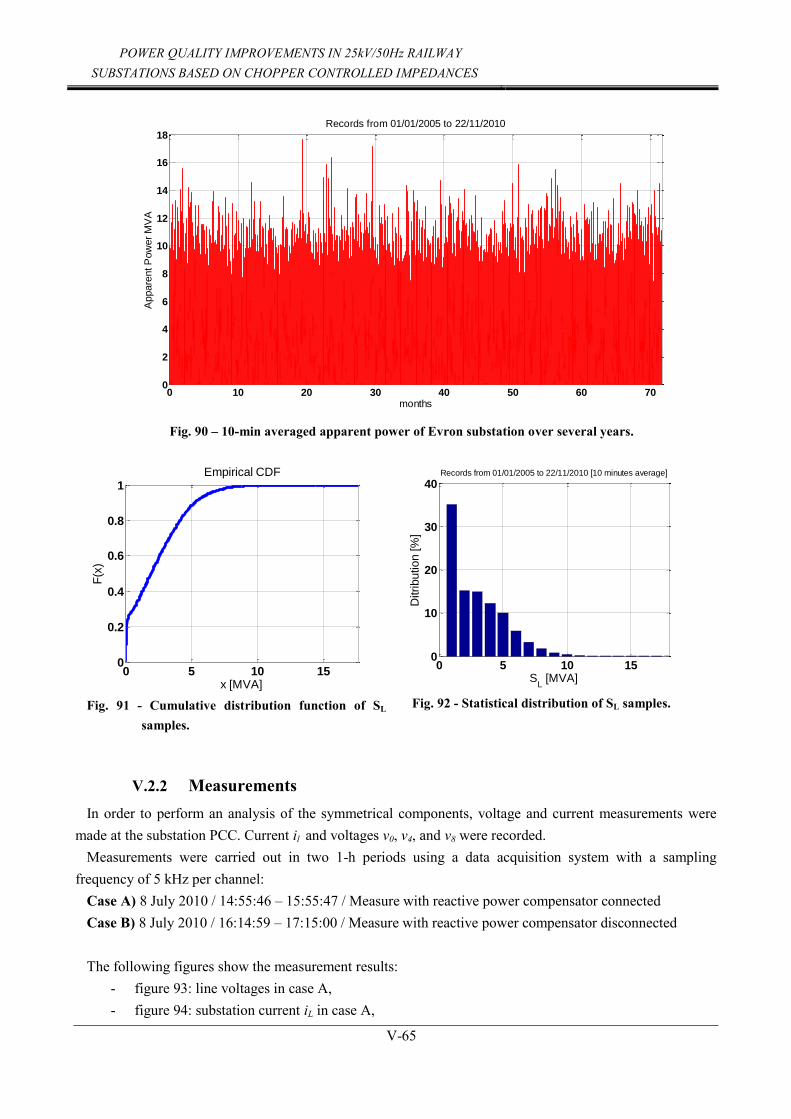
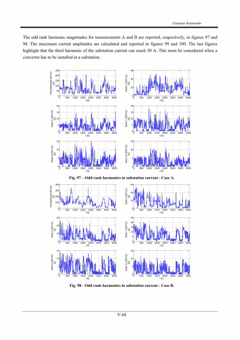
La première partie présente les mesures de puissance active, réactive (Fig. 89) et apparente (Fig. 90) effectués pendant environ 6 ans et moyennées sur 10 minutes. A partir de ces mesures, une analyse statistique (Fig. 91 et 92) montre qu‟une charge de 10MVA peut être considérée comme référence pour dimensionner le compensateur de déséquilibre.
Une analyse harmonique des formes d‟ondes des tensions et des courants mesurées au point de raccordement de la sous station sur le réseau haute tension 90 kV permet d'obtenir des informations utiles pour le dimensionnement du compensateur ainsi que sur le placement des fréquences de résonance des filtres associés aux gradateurs MLI.
Chapitre VI : Compensation des déséquilibres de tension dans la sous-station d’Evron Ce chapitre présente une étude comparative de la solution à impédances contrôlées et de la solution à
onduleurs de tension Le dimensionnement des convertisseurs est basé sur les résultats de l'analyse présentée dans le chapitre précédent. La comparaison est basée sur l'utilisation d‟un même module IGBT (3,3kV/1,5kA).
En premier lieu, ce chapitre décrit le dimensionnement du compensateur sur la base d‟onduleurs de tension
2 niveaux puis 3 niveaux (NPC). Le compensateur est dimensionné pour garantir un taux de déséquilibre de 1.5% lorsque la sous-station alimente une charge de 10MVA à facteur de puissance unitaire dans le cas où la puissance de court-circuit du réseau d'alimentation est de 295MVA (1er mode dégradé).
Afin d'obtenir le niveau de puissance nécessaire, les onduleurs de tension sont connectés en parallèle.
Giuliano Raimondo
xii
Ce chapitre présente le calcul des pertes dans les IGBT pour les deux solutions. Les résultats des calculs analytiques sont validés grâce à l'utilisation du logiciel PSIM et du module thermique.
Le compensateur de déséquilibre basé sur des onduleurs 2 niveaux présente environ 128kW de pertes tandis que la solution à onduleurs NPC présente des pertes totales d‟environ 80kW.
La deuxième partie de ce chapitre concerne l'utilisation du circuit de Steinmetz actif à la sous-station
d‟Evron. La puissance du compensateur est choisie comme dans le cas précédent en fonction de la limite d‟un taux de déséquilibre de tension de 1,5% dans un cas de réseau en mode dégradé.
La solution proposée garantit seulement la compensation de la partie réelle de la composante inverse de
courant. Afin de montrer que cette limitation n‟affecte pas l'efficacité du dispositif, un algorithme numérique (Fig. 127) est utilisé pour simuler la présence du compensateur dans la sous-station pendant 2 heures, en utilisant les mesures effectuées sur le site. Enfin, une analyse statistique réalisée sur six ans d'enregistrements, indique que l'utilisation de la solution proposée garantit une réduction de pénalités dans 98% (fig. 152) des cas.
Les critères de dimensionnement du compensateur de Steinmetz actif tiennent compte du contenu
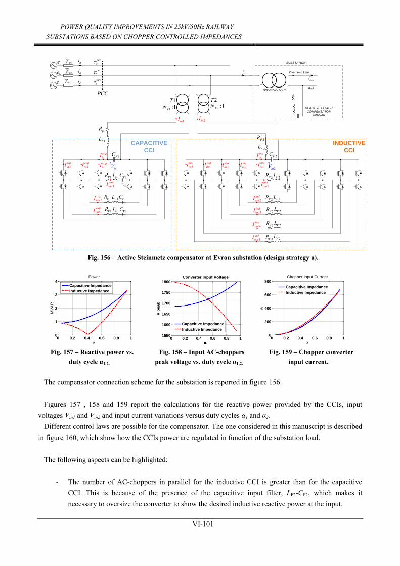
harmonique du courant mesuré à la sous-station. Le schéma final du compensateur pour la sous-station d‟Evron est présenté à la figure 156.
Le calcul analytique des pertes dans les semi-conducteurs est également validé avec le module thermique de PSIM. Elles sont évalués pour cette topologie à environ 61kW.
La synthèse comparative (fig. 167) des pertes totales des trois topologies étudiées montre que pour le
compensateur actif de Steinmetz, celles-ci sont fortement réduites. Les trois topologies sont également comparées en termes d'énergie stockée dans les éléments réactifs (fig. 168). Même dans ce cas la solution à impédance contrôlée par gradateur MLI (Steinmetz Actif) présente des avantages significatifs en termes de volume des éléments réactifs.
Enfin, ce chapitre présente des résultats de simulation de ce nouveau type de compensateur. Ceux-ci
démontrent le bon fonctionnement de la structure même lorsque les formes d'ondes des tensions et des courants sont distordues et conformes à celles relevées sur le site d‟Evron.
POWER QUALITY IMPROVEMENTS IN 25kV/50Hz RAILWAY SUBSTATIONS BASED ON CHOPPER CONTROLLED IMPEDANCES
xiii
Chapitre VII : Compensateur à circuit de Steinmetz actif – Résultats Expérimentaux. Ce dernier chapitre présente les résultats expérimentaux obtenus sur un prototype de compensateur de
Steinmetz actif de puissance réduite ( 1.5kVA), réalisé au laboratoire LAPLACE à Toulouse. La figure 175 montre un schéma du dispositif expérimental. Un autotransformateur est utilisé pour obtenir
une source triphasée. Deux gradateurs MLI (inductifs et capacitifs) sont réalisés avec des IGBT sur circuit imprimé et une résistance de 2.2 kW est utilisée comme charge monophasée. Les essais ont été effectués sous une tension de 300V. Une carte dSPACE est utilisée pour contrôler les gradateurs (fig. 180). Celle-ci assure un contrôle en boucle fermée de la valeur efficace du courant dans les impédances contrôlées.
Le chapitre montre les grandeurs fondamentales avant et après la compensation. La charge monophasée provoque un déséquilibre des tensions d'environ 2,1% (fig. 181). Lorsque le compensateur est activé, le taux de déséquilibre est ramené à 0,55% (fig. 184). Ce qui valide le bon fonctionnement du compensateur.
Conclusion & Perspectives Suite à l‟augmentation du trafic ferroviaire, les sous-stations SNCF 25kV/50Hz sont de plus en plus
concernées par les problèmes de qualité de l‟énergie électrique. Dans la plupart des cas, afin de respecter les limites imposées par le fournisseur d'énergie ou de garantir le bon fonctionnement du réseau ferroviaire lui-même, l'opérateur des chemins de fer est obligé d'installer des dispositifs électroniques de puissance dans la sous-station.
Deux principaux types de dispositifs sont installés aujourd'hui sur le réseau ferré Français: les
compensateurs de puissance réactive et les compensateurs de déséquilibre de tension Les premiers permettent d'éviter des pénalités imposées par le fournisseur d'énergie et liées à la
dégradation du facteur de puissance. En plus, ils peuvent réguler la tension de caténaire lorsque le trafic augmente. Cela permet d'éviter que la tension de la caténaire ne descende en dessous du minimum imposé par les normes internationales (19kV).
Les compensateurs de déséquilibre de tension permettent d'augmenter la capacité de la sous-station sans
dépasser la limite du taux de déséquilibre fixé par le fournisseur d'énergie. L'opérateur des chemins de fer peut choisir entre plusieurs topologies de compensateurs disponibles.
Néanmoins, chaque topologie détermine une augmentation du coût de fonctionnement de la sous-station, notamment en raison des pertes dans les convertisseurs.
Dans le cadre de ce travail de thèse, nous avons proposé l'utilisation de nouvelles topologies de
compensateurs pour les sous-stations 25kV/50Hz. Les impédances contrôlées par gradateur MLI sont des structures caractérisées par de faibles pertes dans les semi-conducteurs et nécessitent des éléments réactifs de volume réduits par rapport aux solutions classiques.
La nouvelle solution proposée est analysée pour la compensation de puissance réactive et la compensation de déséquilibre. Les critères de dimensionnement sont présentés en utilisant les informations obtenues par
Giuliano Raimondo
xiv
des mesures dans deux sous-stations de la SNCF considérés comme cas typiques. Les résultats des simulations et les résultats expérimentaux valident le principe de fonctionnement de ces compensateurs.
Pour la compensation de déséquilibre, le compensateur de Steinmetz actif parait donc très attractif pour les
opérateurs ferroviaires. Les faibles pertes permettent une réduction importante des coûts de fonctionnement et d'entretien de la sous-station alors que le volume réduit des éléments réactifs détermine un coût d'achat plus bas.
Une étude comparative entre la nouvelle topologie et la solution classique à onduleurs montre que les
pertes sont réduites d'environ 60% et l'énergie stockée dans les éléments réactifs est réduite d‟un facteur six. Depuis dix ans, les solutions à thyristors et onduleurs de tension ont été utilisées et évaluées sur le Réseau
Ferré National Français. Logiquement, dans un avenir proche, un compensateur de déséquilibre basé sur les impédances contrôlées par gradateur MLI pourrait donc être construit et installé dans une sous-station.
POWER QUALITY IMPROVEMENTS IN 25kV/50Hz RAILWAY SUBSTATIONS BASED ON CHOPPER CONTROLLED IMPEDANCES
xv
RIASSUNTO DELLA TESI IN LINGUA ITALIANA
Capitolo I: Introduzione Il primo capitolo introduce brevemente il sistema ferroviario della SNCF e in particolare la rete alimentata
da sottostazioni a 25kV/50Hz. L‟interesse nell‟installazione di dispositivi di elettronica di potenza nelle sottostazioni in corrente alternata
è aumentato notevolmente negli ultimi anni. I convertitori infatti consentono di rispettare i requisiti sulla qualità dell‟energia imposti dal fornitore dell‟energia elettrica ed inoltre di garantire il buon funzionamento della sottostazione stessa.
Attualmente 2 tipi di compensatori sono installati nelle sottostazioni della SNCF (Fig. 3): - Compensatori di potenza reattiva:
Consentono di evitare le penali imposte dal fornitore dell‟energia elettrica quando si scende al di sotto del valore minino del fattore di potenza. Inoltre, in caso di elevato traffico, consentono di aumentare la tensione di catenaria quando questa diminuisce a causa delle perdite sulla linea, evitando che possa scendere al di sotto del limite imposto (19kV). Sono in genere installati al secondario del trasformatore di sottostazione.
- Compensatori di squilibri di tensione
Hanno lo scopo di ridurre la sequenza inversa di corrente assorbita dalla sottostazione al fine di ridurre il fattore di squilibrio al punto di connessione del primario del trasformatore di sottostazione. Sono in genere connessi direttamente alla rete di trasmissione in alta tensione.
Le soluzioni attualmente impiegate dalla SNCF nel caso della potenza reattiva fanno uso di convertitori
basati su tiristori oppure di batterie di compensazione capacitive fisse. Nel caso della compensazione degli squilibri la soluzione adottata è basata su Voltage Source Inverter (VSI).
Queste soluzioni soffrono di notevoli svantaggi. La compensazione con batterie fisse, è economica ma non consente una compensazione variabile in
funzione del carico. Le soluzioni a tiristori sono caratterizzate da una notevole distorsione armonica a bassa frequenza della
corrente che rende necessaria l‟installazione di filtri voluminosi. Infine, la topologia VSI ha il forte inconveniente di avere elevate perdite nei semiconduttori che rendono
necessaria l‟installazione di grossi sistemi di raffreddamento, aumentando i costi di gestione e funzionamento della sottostazione. Inoltre, nella compensazione degli squilibri, questi convertitori richiedono condensatori di capacità elevata sul bus DC. Questo per ridurre l‟elevata ondulazione di tensione dovuta dalla potenza fluttuante legata alla sequenza inversa di corrente che si inietta.
Giuliano Raimondo
xvi
Capitolo II: Il concetto di Impedenza Controllata mediante PWM AC Chopper Il capitolo introduce il concetto di Impedenza Controllata mediante AC Chopper (CCI - Chopper
Controlled Impedance). Convertitori AC/AC di tipo PWM AC Chopper vengono impiegati per realizzare impedenze controllate (induttive o capacitive) alla frequenza fondamentale.
La struttura del convertitore (Fig. 29) prevede 2 celle switching comandate in PWM in funzione del segno della tensione di ingresso (Fig. 31).
Vengono presentate due possibili modalità di funzionamento, step-down (Fig. 33) o step-up (Fig. 34) che consentono di ottenere due differenti leggi di variazione del modulo dell‟impedenza controllata (Table I).
In applicazioni di elevata potenza, l‟associazione dei convertitori in parallelo (Fig. 40) o in serie (Fig. 42) è possibile, consentendo di ottenere i livelli di potenza richiesti e di superare i problemi di elevate tensioni. Inoltre interallacciando le PWM dei moduli si ha un miglioramento della qualità della corrente o tensione, avendo una frequenza di switching apparente più elevata.
La topologia di convertitori introdotta nel capitolo, può rappresentare una soluzione interessante come alterativa a quelle attualmente impiegate. Infatti, rispetto alle soluzione a tiristori, gli AC Chopper non generano armoniche di corrente a bassa frequenza. Inoltre, confrontate con soluzioni basate su VSI, le perdite nei semiconduttori sono notevolmente ridotte negli AC-Chopper, e anche gli elementi reattivi impiegati sono di minor volume.
Capitolo III: Compensazione della potenza reattiva mediante l’impiego di Impedenze Controllate Il capitolo propone l‟impiego delle impedenze controllate mediante chopper nella compensazione della
potenza reattiva nelle sottostazioni. La sottostazione della SNCF di Revest è considerata come caso studio. Si tratta di una sottostazione di
60MVA connessa ad una linea alta tensione a 225kV (Fig. 44). Nel capitolo viene sviluppato uno studio di fattibilità di installazione nella sottostazione in oggetto di un compensatore di potenza reattiva basato su CCI.
Nella prima parte, vengono presentate le misure effettuate duranti diversi mesi sul sito della SNCF. Queste consentono di ricavare informazioni utili al dimensionamento del compensatore. Infatti, l‟analisi armonica della corrente assorbita dalla sottostazione consente di posizionare le risonanze introdotte in intervalli di frequenze ammissibili. Inoltre, da una analisi statistica sulla riduzione delle penalità imposte sul fattore di potenza, viene determinata la taglia del compensatore variabile da installare (Fig. 50).
Vengono presentate due possibili soluzioni basate sulla modalità di funzionamento step down (Fig. 51) e step-up (Fig. 58) e i relativi criteri di progetto.
La soluzione basata sul modo di funzionamento step-up risulta più interessante, consentendo una installazione transformeless nella sottostazione. Per questa configurazione, si riporta il risultato di alcune simulazioni effettuate considerando forme d‟onda reali per correnti e tensione misurate nella sottostazione. Infine, si presentano i risultati sperimentali ottenuti su un prototipo da 1.2MVAR (Fig. 67) nel centro di prove della SNCF a Vitry.
POWER QUALITY IMPROVEMENTS IN 25kV/50Hz RAILWAY SUBSTATIONS BASED ON CHOPPER CONTROLLED IMPEDANCES
xvii
Capitolo IV: Compensazione degli squilibri di tensione impiegando il circuito di Steinmetz attivo a
impedenze controllate. In questo capitolo, il concetto di impedenza controllata da chopper viene applicato nella compensazione
degli squilibri di tensione. Il circuito di Steinmetz (Fig. 80) viene utilizzato per connettere carichi monofase ad una rete trifase.
Consiste in un induttore ed un condensatore opportunamente dimensionati e connessi al carico monofase al fine di renderlo equilibrato nei confronti della rete trifase. Questa tecnica di compensazione, facendo uso di semplici elementi reattivi risulta efficace solo se il carico è fisso. Nel caso di una sottostazione in cui l‟assorbimento di potenza dipende dal traffico ferroviario, questa soluzione risulta chiaramente poco adatta.
Impiegando le impedenze controllate da chopper, viene proposto nel capitolo un circuito di Steinmetz attivo (Fig. 83). In funzione della potenza assorbita dalla sottostazione, le impedenze controllate assumono i valori necessari alla compensazione dello squilibrio generato.
Questa soluzione, ha però lo svantaggio di compensare sequenze inverse solo in una regione limitata del piano complesso (Fig. 86). Inoltre, se non si vuole degradare il fattore di potenza trifase, allora solo la parte reale della componente simmetrica inversa deve essere compensata (Fig. 87). Questo quindi, rende il dispositivo poco adatto nelle applicazioni dove una compensazione degli squilibri istantanea è richiesta.
Nel caso delle sottostazioni ferroviarie, una compensazione media è sufficiente a rispettare i limiti, imposti su medie di 10 minuti. Inoltre, le vecchie locomotive in funzione saranno sempre meno col passare del tempo, in quanto sostituite da nuovi modelli equipaggiati da convertitori di trazione a fattore di potenza unitario. Di conseguenza, è necessario compensare solo la parte reale della componente simmetrica inversa di corrente assorbita.
Tuttavia, a fronte dello svantaggio legato al dominio di compensazione limitato, questa soluzione presenta dei notevoli vantaggi economici rispetto alle soluzioni classiche. Questo aspetto verrà dettagliato nel capitolo VI.
Capitolo V: Analisi della qualità dell’energia elettrica in una sottostazione La sottostazione della SNCF di Evron (schema in figura 88) viene considerata come caso di studio per la
compensazione degli squilibri di tensione. In tal senso, il capitolo presenta una analisi su misure effettuate sul sito della SNCF al fine di ricavare informazioni utili al dimensionamento del compensatore.
Nella prima parte vengono riportate le misure di potenza attiva,reattiva(Fig. 89) e apparente (Fig. 90) effettuate durante circa 6 anni, su medie di 10 minuti. Da queste si ricava mediante un‟analisi statistica che un carico da 10MVA può essere considerato come riferimento nella scelta della taglia del compensatore.
In seguito viene presentata un‟analisi armonica delle tensioni e correnti misurate al punto di connessione in alta tensione della sottostazione durante 2 ore. Questo al fine ottenere informazioni utili a progettare il sistema in modo che le eventuali risonanze introdotte siano in intervalli di frequenza consentiti.
Infine, viene riportato il risultato del calcolo della componente simmetrica inversa della corrente assorbita.
Giuliano Raimondo
xviii
Capitolo VI: Compensazione degli squilibri di tensione nella sottostazione di Evron Il capitolo VI presenta uno studio comparativo tra la soluzione basata su circuito di Steinmetz attivo e le
soluzioni classiche basate su VSI. Il dimensionamento dei convertitori è basato sui dati provenienti dalle analisi riportate nel capitolo precedente. Il confronto è basato sull‟impiego nelle tre soluzioni dello stesso dispositivo IGBT.
In primis, si descrive il dimensionamento del compensatore basato su VSI 2 livelli e NPC 3 livelli. Il
compensatore è dimensionato per garantire un fattore di squilibrio dell‟1.5% quando la sottostazione è interessata da un carico da 10MVA a fase nulla, quando la potenza di corto circuito del sistema elettrico è quella minima ipotizzata a 295MVA. Una struttura di moduli VSI associati in parallelo è necessaria per ottenere la potenza di dimensionamento richiesta.
A valle del dimensionamento, viene riportato il calcolo delle perdite negli IGBT per le due soluzioni e se ne validano i risultati mediante l‟impiego del simulatore circuitale PSIM e il tool Thermal Module. In totale, il compensatore di squilibri basato su VSI 2 livelli risulta avere perdite per 128kW. Mentre per la soluzione a VSI 3 livelli NPC, le perdite totali ammontano a circa 80kW.
Nella seconda parte si analizza l‟impiego del circuito di Steinmetz attivo ad Evron. La taglia del
convertitore è scelta come nel caso precedente sulla base del limite del fattore di squilibrio delle tensioni al 1.5% con una potenza di corto circuito minima di 295MVA.
La soluzione proposta, garantisce una compensazione media, in quanto solo la parte reale della componente simmetrica inversa viene ridotta. Al fine di mostrare che questo limite non ne influenzi l‟efficacia, un algoritmo numerico (Fig. 127) viene usato per simulare la presenza del compensatore nella sottostazione durante 2 ore, usando le misure effettuate sul sito.
Infine, un‟analisi statistica effettuata su sei anni di registrazioni, indica che impiegando la soluzione proposta si ha una riduzione delle penalità del 98% circa (Fig. 152).
In seguito vengono mostrati i criteri di dimensionamento che tengono conto della conoscenza del
contenuto armonico della corrente della sottostazione. Lo schema finale del compensatore si Steinmetz attivo per la sottostazione di Evron è presentato in figura 156.
Il calcolo delle perdite, validato anche in questo caso mediante il Thermal Module di Psim, si valutano per questa topologia a circa 61kW.
Una sintesi comparativa (Fig. 167) tra le perdite delle tre topologie di compensatore analizzate mostrano come, per il circuito di Steinmetz attivo, queste siano notevolmente ridotte. Le tre topologie, vengono anche confrontate in termini di energia immagazzinata negli elementi reattivi (Fig. 168). Anche in questo caso la soluzione proposta mostra notevoli vantaggi in termini di dimensione degli elementi reattivi.
Infine, il capitolo riporta il risultato di alcune simulazioni del compensatore proposto. Queste, dimostrano
il corretto funzionamento della soluzione basata sulle impedenze controllate anche quando vengono considerate come forme d‟onda di tensioni e corrente quelle misurate sul sito della SNCF.
POWER QUALITY IMPROVEMENTS IN 25kV/50Hz RAILWAY SUBSTATIONS BASED ON CHOPPER CONTROLLED IMPEDANCES
xix
Capitolo VII: Circuito di Steinmetz attivo – Prove sperimentali L‟ultimo capitolo presenta i risultati sperimentali ottenuti su un prototipo di compensatore di Steinmetz
attivo di potenza ridotta (1.5kVA) realizzato al LAPLACE di Toulouse. Figura 175 mostra uno schema dell‟apparato sperimentale. Un autotrasformatore è impiegato per ottenere
una alimentazione trifase, due AC Chopper (induttivo e capacitivo) sono realizzati mediante IGBT e un carico resistivo da 2.2kW è impiegato come carico monofase. I test sono stati effettuati a 300V. Un dSPACE è utilizzato per il controllo del convertitore (Fig. 180). In particolare viene eseguito un controllo a ciclo chiuso del valore rms delle correnti delle due impedenze controllate.
Vengono riportate le registrazioni delle grandezze fondamentali prima e dopo la compensazione dello squilibrio. Il carico monofase determina uno squilibrio delle tensioni pari a circa il 2.1% (Fig. 181). Quando il compensatore è attivato il fattore di squilibrio scende a circa 0.55% (Fig. 184).
In conclusione, il corretto funzionamento del compensatore di Steinmetz attivo è validato. Conclusioni e Prospettive
In seguito all'aumento del traffico ferroviario, le sottostazioni della SNCF 25kV/50Hz si trovano sempre più ad affrontare problemi di power quality. In molti casi, al fine di rispettare i vincoli imposti dal fornitore dell‟energia elettrica o di garantire il buon funzionamento del sistema ferroviario stesso, l‟operatore è obbligato a installare dei convertitori di elettronica di potenza nella sottostazione.
I dispositivi installati oggi nelle sottostazioni del sistema francese, sono essenzialmente due: i
compensatori di potenza reattiva e i compensatori di squilibri di tensione. I primi permettono di evitare le penalità imposte dal fornitore dell‟energia elettrica legate alla riduzione del
fattore di potenza. Inoltre, possono regolare la tensione di catenaria quando a seguito di una aumento del traffico ferroviario. Questa operazione permette di evitare che la tensione di catenaria possa scendere al di sotto del minimo imposto dalle norme internazionali (19kV).
I compensatori di squilibri di tensione permettono di aumentare la capacità della sottostazione evitando di
oltrepassare il limite sul fattore di squilibrio fissato dal fornitore dell‟energia elettrica. Le topologie di compensatori che l‟operatore ferroviario può impiegare nelle sottostazioni sono molteplici.
Tuttavia, ogni topologia determina un aumento dei costi di funzionamento della sottostazione a causa delle perdite nei convertitori.
In questo lavoro di tesi, viene proposto l‟utilizzo di nuove topologie di compensatori per le sottostazioni
25kV/50Hz. Le impedenze controllate mediante PWM AC Chopper sono strutture di conversione caratterizzate da basse perdite nei semiconduttori e necessitano di elementi reattivi di volume ridotto rispetto alle soluzioni classiche.
La nuova soluzione proposta è analizzata per la compensazione della potenza reattiva e degli squilibri di tensione. I criteri di dimensionamento presentati sono basati su informazioni ottenute da misure effettuate in
Giuliano Raimondo
xx
due sottostazioni della SNCF considerate come caso studio. I risultati delle simulazioni e i risultati sperimentali validano il principio di funzionamento di questi compensatori.
Per la compensazione degli squilibri, il compensatore di Steinmetz attivo è di grande interesse per gli
operatori ferroviari. Le basse perdite permettono una riduzione importante dei costi di funzionamento e manutenzione della sottostazione. Inoltre, il volume ridotto degli elementi reattivi determina un costo d‟acquisto inferiore.
Uno studio comparativo tra la nuova topologia e la soluzione classica basata sull‟uso di Voltage Source
Inverter, mostra che le perdite sono ridotte di circa il 60% e l‟energia immagazzinata negli elementi reattivi è ridotta di circa un fattore sei.
Negli ultimi dieci anni, le soluzioni a tiristori e a voltage source inverter sono state impiegate e valutate nel
sistema ferroviario francese. Dunque, a breve un compensatore di squilibri basato su impedenze controllate mediante PWM AC Chopper potrebbe essere realizzato e installato in una sottostazione.
POWER QUALITY IMPROVEMENTS IN 25kV/50Hz RAILWAY SUBSTATIONS BASED ON CHOPPER CONTROLLED IMPEDANCES
xxi
Content
CHAPTER I. INTRODUCTION ............................................................................................. I-1
I.1 THE RAILWAY SUPPLY SYSTEM 25kV/50Hz ......................................................................................... I-1
I.1.1 The SNCF electric railways systems ......................................................................................................... I-1
I.1.2 Power Electronics in the SNCF 25kV/50Hz railways system ................................................................... I-2
I.2 Reactive Power compensation ......................................................................................................................... I-3
I.2.1 Reactive power compensator devices installed in SNCF substations ........................................................ I-4
I.3 Voltage Unbalance Compensation .................................................................................................................. I-7
I.3.1 Introduction to unbalance .......................................................................................................................... I-7
I.3.2 Characterization of the unbalance .............................................................................................................. I-8
I.3.3 Current Unbalance ..................................................................................................................................... I-9
I.3.4 Voltage Unbalance ................................................................................................................................... I-10
II.1.2 Overview of single-phase PWM AC Choppers Topologies ................................................................... II-20
II.2 Practical applications of single-phase AC Choppers .............................................................................. II-23
II.2.1 Step-down or step-up AC Chopper ......................................................................................................... II-23
II.2.2 Concept of controlled impedance ........................................................................................................... II-24
II.2.3 Active voltage divider ............................................................................................................................. II-24
II.3 Application of the controlled impedance concept ................................................................................... II-27
II.3.1 Choice of the structure ............................................................................................................................ II-27
III.2 Case study–Revest substation................................................................................................................. III-32
III.2.1 Current and voltage measurements .................................................................................................... III-32
III.2.2 Current analysis ................................................................................................................................. III-32
III.2.3 Power analysis ................................................................................................................................... III-34
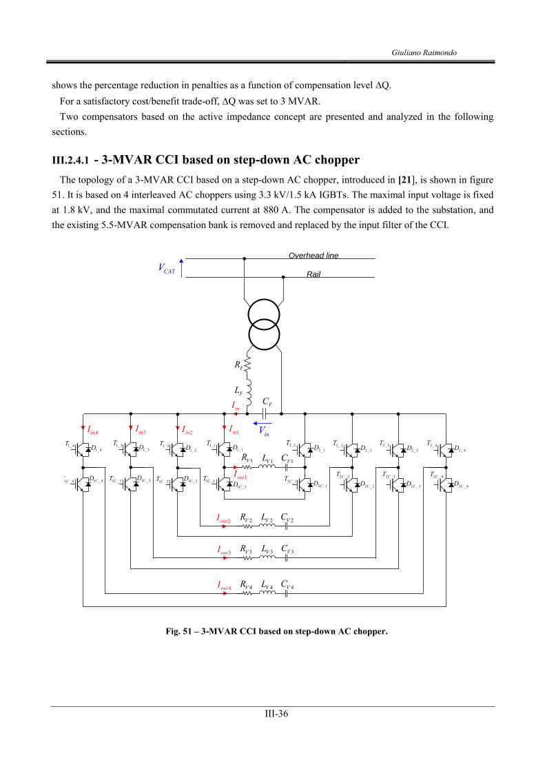
III.2.4 Reactive power compensator ............................................................................................................. III-35
CHAPTER IV. VOLTAGE UNBALANCE COMPENSATION BASED ON CCI: ACTIVE STEINMETZ COMPENSATOR ............................................................................................. IV-51
IV.1 Unbalance compensation based on active Steinmetz circuit ................................................................ IV-51
CHAPTER VI. VOLTAGE UNBALANCE COMPENSATION IN EVRON SUBSTATION ..................................................................................................................... VI-75
VI.1 Voltage Unbalance compensation in Evron substation based on Voltage Source Inverter .............. VI-75
VI.2.4 Power losses .................................................................................................................................... VI-105
VI.3 Comparison of VSI vs. active Steinmetz.............................................................................................. VI-107
POWER QUALITY IMPROVEMENTS IN 25kV/50Hz RAILWAY SUBSTATIONS BASED ON CHOPPER CONTROLLED IMPEDANCES
CHAPTER VII. ACTIVE STEINMETZ COMPENSATOR-EXPERIMENTAL RESULTS ................................................................................................................. VII-114
VII.3 Control .................................................................................................................................................. VII-117
APPENDIX I SEMICONDUCTOR POWER LOSSES AND THERMAL LIMITS ...... AI-1
APPENDIX II DC-LINK CAPACITOR SELECTION IN VOLTAGE UNBALANCE COMPENSATOR BASED ON VSI .......................................................................................... AII-1
Giuliano Raimondo
xxiv
POWER QUALITY IMPROVEMENTS IN 25kV/50Hz RAILWAY SUBSTATIONS BASED ON CHOPPER CONTROLLED IMPEDANCES
I-1
Chapter I. Introduction In this chapter, the application of power electronic devices in the SNCF 25kV/50Hz railways is discussed.
The traffic increasing makes hard for railways operator to handle power quality issues and the respect of the functioning range of electrical parameters requested from european standards.
The installation of power converters can avoid expensive infrastructure modifications, as installation of extras substations or building new power transmission line.
The subject is investigated in this chapter in three parts. Firstly, an introduction of the SNCF AC 25kV/50Hz network is pointed out. Following, in the last two parts, a discussion about the advantages leads by reactive power and voltage unbalance compensation is developed.
I.1 THE RAILWAY SUPPLY SYSTEM 25kV/50Hz
I.1.1 The SNCF electric railways systems The SNCF railway network is basically supplied by 1500V DC voltage and 25kV/50Hz single phase
voltage [1]. The railways electrification in France started at the beginning of the 20th century with the 1.5kV DC. The
overhead lines are supplied by means of transformer/rectifier groups connected to the three-phase HV network 63kV or 90kV (figure 1). The distance between substations in is in the range 8-25 km, according to the nominal power. The power draws by substations is up to 15MW.
Regarding the AC 25kV/50Hz system, it debuts in 1954 with the line Valenciennes – Thionville. Overhead lines are supplied using substations equipped by single phase transformers whose the primary is connected to the HV transmission network 63kV to 400kV (figure 2). These substations are placed at distance of about 35km to 90km according to the installation power. Generally, substations nominal power can reach 70MVA.
Compared to 1.5kV DC, the 25kV/50Hz single phase railways system allows economical advantages for the infrastructures of about 30% in terms of investment, exploitation and maintenance.
Fig. 1 - 1.5kV railways electrification system
Fig. 2 - 25kV/50Hz AC railways electrification system
Substation 1
Transformer
HV transmission
network
HV transmission
network8km ~ 25km
Overhead line
1.5kV DC
Substation 2
Transformer
Substation 1
Transformer
HV transmission
network
Substation 2
Transformer
HV transmission
network35km ~ 90km
Overhead line
25kV/50Hz
Giuliano Raimondo
I-2
I.1.2 Power Electronics in the SNCF 25kV/50Hz railways system While in DC system, power electronics has been used for more than 50 years through AC/DC rectifiers, in
AC system, due to its very simple diagram, there was until now no necessity to integrate power electronics in substations.
However, for the next decades, due to difficulties in funding and also in environmental integration, power electronics can provide the solution for network optimisation when traffic increases or when a difficulty appears for a substation implementation. Nowadays, in AC electrification, two main types of devices are implemented:
- Reactive Power compensators/High Voltage Boosters - Three phase line Balancers.
Basically the first device satisfies two objectives. Firstly, it compensates losses in the rail network by
injecting reactive energy in order to keep the overhead line voltage in the admissible range [19kV – 29kV] for locomotives. Moreover, as several old locomotives work with a low power factor, reactive power compensation in substations is achieved in order to reduce penalties from the energy provider. In order to avoid this problem, new generation of SNCF locomotives are equipped by unity power factor rectifiers based on Voltage Source Inverters.
The second device allows, in case of weak three-phase public network to enhance the substation power
load without exceeding the unbalance limit imposed by the energy provider. In fact, a strong drawback of the AC system is that the substations are phase to phase connected to transmission lines which generates voltage unbalance in high load conditions.
The two compensation systems introduced previously are commonly installed on the railway network as
reported in figure 3. These aspects are discussed in detail in the next sections.
Fig. 3 – Power Electronics devices in 25kV/50Hz railways
Substation 1
Transformer
HV transmission
network
Substation 2
Transformer
Overhead line 25kV/50Hz
Reactive Power
Compensator
Reactive Power
Compensator
Unbalance
CompensatorHV transmission
network
POWER QUALITY IMPROVEMENTS IN 25kV/50Hz RAILWAY SUBSTATIONS BASED ON CHOPPER CONTROLLED IMPEDANCES
I-3
I.2 Reactive Power compensation With the aim of understanding the necessity of reactive power compensators in the SNCF railways
network, the influence of locomotives in the traction system is discussed. A simple scheme of a supply circuit of a traction system is reported in figure 4. The equivalent circuit at
grid frequency is shown in figure 5. With: uHV: line to line voltage of the three-phase transmission network at the substation coupling point. RHV, XHV: respectively line resistance and line reactance of the three-phase transmission network mss: substation transformer ratio Rss, Xss: leakage transformer resistance and reactance view at the secondary side vcat: voltage between overhead line and rail iss: current drawn at the secondary of the substation transformer
Fig. 4 - a supply circuit of a traction system
Fig. 5 - equivalent circuit at grid frequency On this base, the equivalent Thevenin circuit can be pointed out in figure 6.
Fig. 6 - Equivalent Thevenin circuit of the substation
The expressions for equivalent reactance Xsec and equivalent resistance Rsec are the following:
ssHVss XXmX 2sec 2 (1)
ssHVss RRmR 2sec 2 (2)
The rms value of voltage vcat0 is the rms value of the voltage at secondary side of the transformer in open-circuit condition:
0 0cat ss HVV m U (3)
Substation
Transformer
HV trasmission
network (uHV)
Overhead line
25kV/50Hz
Rail
iss
vcat
Pcat, Qcat
Pss, Qss
Energy Meter
0HVu
HVXHVR
HVXHVR
ssXssR
HVu
ssm
catvss HVm u
ssi
0catv
secXsecR
catv
ssi
Giuliano Raimondo
I-4
The Fresnel diagram of the traction circuit is reported in figure 7. Considering the projection on real and imaginary axis, the following equations are obtained:
0 sec seccos sin cosss HV ss ss catm U X I R I V (4)
0 sec secsin cos sinss HV ss ssm U X I R I (5)
Fig. 7 - Fresnel Diagram
On the assumption that the voltage drop V is low regarding the nominal voltage, the angle is small. On this base, a good approximation for the voltage drop is:
0 sec secsin cosss HV cat ss ssV m U V X I R I (6)
This can be rearranged as following:
0 sec seccat cat
ss HV catcat cat
Q PV m U V X RV V
(7)
Where Qcat and Pcat are respectively reactive and active power drawn by the trains. Let‟s note from the previous equations, where voltage UHV0 is assumed as constant, that in case of high
power drawn by the trains, the overhead line voltage drop down and can decrease under the minimum value of 19kV imposed by the european standard EN50163 [2]. Thus, in substations supplying high traffic lines, in order to guarantee the locomotives operation, it is mandatory to install reactive power compensator acting as voltage booster devices.
Moreover, to limit losses and voltage drop on transmission lines, the electric energy provider imposes a minimum value for the substation displacement factor. Penalties are applied on reactive energy when this limit is passed. Thus, penalties are avoided or reduced by installing a reactive power compensator device.
I.2.1 Reactive power compensator devices installed in SNCF substations Currently, two types of reactive power compensation are installed in the SNCF 25kV/50Hz network. The
first is a fixed compensation based on capacitive shunt filters. The second is a variable compensation based on a thyristor controlled reactance (TCR). At the moment, the synchronous static compensator (called STATCOM) based on Voltage Source Inverter is not used by the SNCF.
catV
ssI
sec ssR Isec ssjX I
0HVssm U
Im
Re
POWER QUALITY IMPROVEMENTS IN 25kV/50Hz RAILWAY SUBSTATIONS BASED ON CHOPPER CONTROLLED IMPEDANCES
I-5
I.2.1.1 Fixed Compensation In most cases, reactive power compensation in railways is achieved by connecting shunt capacitive filters
to the substation. These filters, as reported in figure 8, consist of an inductor Lfix and a capacitor Cfix connected in series. They are placed at the secondary side of the substation transformer between the overhead line and the rail.
The reactive power provided by the fixed compensation device is:
2
21cat fix net
compfix fix net
V CQ
L C
(8)
Where net is the grid angular frequency. This solution is very straightforward and economical but unsuitable for large reactive power fluctuations.
In fact, when the substation is lightly charged, the reactive power is overcompensated and the overhead line voltage exceeds the limit imposed (29kV) by the EN 50_163 standard.
In this case, a variable reactive power compensation system is needed, in order to adapt the level of compensation to the substation load.
Fig. 8 - Scheme of a substation equipped by fixed reactive power compensation device
I.2.1.2 Variable compensation Currently, the SNCF used three variable reactive power compensators based on TCRs. The first one was
built in the frame of the European project HVB (High Voltage Booster) started in 1998 [3]. The aim of this project was to provide a device able to instantaneously compensate the overhead line voltage drop in function of the train traffic. This compensator was commissioned in 2002 [4]. A scheme of a substation using this solution is presented in figure 9. Basically, the converter topology is composed by a fixed capacitive filter, a single phase TCR that acts as a variable inductor at the grid frequency and a bulky LC filter tuned on
Substation
Transformer
HV transmission
network
Overhead line
25kV/50Hz
Rail
iss
vcat
fixL
fixC
Shunt
Capacitive
Filter
itrain
Giuliano Raimondo
I-6
the third harmonic (150 Hz). Pictures of the reactive elements of the compensators are presented in figures 10 and 11.
Fig. 9 – Substation equipped by variable reactive power compensator based on thyristors SVC
Fig. 10 – Inductor Lvar
Fig. 11 – Shunt Filter Cfix - Lfix
This TCR allows the variation of the fundamental lagging current by phase-control, counterbalancing large
leading currents from associated fixed capacitors and allowing a continuous compensation of the lagging reactive power. However this solution generates a high level of low rank harmonics and requires onerous LC filters. Moreover, it should be notice that, due to the functioning principle of this compensator, the power losses in semiconductor devices are highest when no compensation is required [5].
Substation
Transformer
HV transmission
network
Overhead line
25kV/50Hz
Rail
iss
vcat
fixL
fixC
Shunt
Capacitive
Filter
itrain
varL
fixC
filterL
filterC
SVC
POWER QUALITY IMPROVEMENTS IN 25kV/50Hz RAILWAY SUBSTATIONS BASED ON CHOPPER CONTROLLED IMPEDANCES
I-7
I.3 Voltage Unbalance Compensation In 25 kV/50 Hz railways, the substations are phase to phase connected to transmission lines. They behave
as nonlinear and time-varying loads and represent one of the most important sources of voltage unbalance regarding the electricity transmission network
In case of weak networks, railways operators are required to install compensation systems in substations in order to satisfy limits and to avoid penalty. The limits are established by the energy provider with a view to guarantee a sufficient voltage quality to other customers.
Unbalance compensation systems are necessary when the railways operator is interested in increasing traffic on a line and the electric transmission network is not enough “strong” to support a larger load. It is evident that if the voltage unbalance compensation is achieved, the construction of a new transmission line can be avoided, resulting in considerable economical advantages.
In order to understand the phenomenon, some concepts of voltage unbalance theory are pointed out in the
following discussions.
I.3.1 Introduction to unbalance A three-phase AC power system is balanced when the three voltages and currents have equal magnitudes
and 120° phase-displacements, otherwise it is unbalanced. Unbalanced voltages can produce adverse effects on equipment and on the power system. A small
unbalance in the phase voltages can cause an extremely large unbalance in the phase currents and the power system will incur more losses and heating effects. The effect of voltage unbalance can also be severe on equipment such as induction motors, power electronic converters and adjustable speed drives (ASDs) [6].
At the medium and high voltage levels the AC loads phase to phase connected are rare [7]. Some typical loads in this category are as follows:
– traction supplies, – arc furnaces, – resistance melting furnaces, – heavy-current test systems. AC railway substations, especially for high-speed railway, represent large single-phase loads which draw
considerable unbalanced currents from the power-supply system, leading to voltage unbalance. Figure 12 shows a three phase power systems feeding a single phase substation. Due to the voltage drop on
line impedances, PCC voltages pcc pcc pcca b ce e e
are unbalanced.
Giuliano Raimondo
I-8
Fig. 12 - Simple traction connection scheme
I.3.2 Characterization of the unbalance The definition of the voltage unbalance is based on the representation of the three-phase system in the form
of symmetrical components. According to Fortescue theory, unbalanced three-phase phasors
1 2 3E E E
can be decomposed into three symmetrical phasors named positive, negative and zero-
sequence components 0E E E
.
Thus, the unbalanced system can be split up into 3 balanced systems: - a balanced system having the same phase sequence as the unbalanced system:
1
22
3
E E
E E
E E
(9)
- a balanced system having the opposite phases sequence to the unbalanced system (rotation of phasors is always anticlockwise, it is the order of the phases that changes, and not the direction of rotation):
1
2
23
E E
E E
E E
(10)
- a balanced system of in-phase quantities:
10 0
20 0
30 0
E E
E E
E E
(11)
where α is the rotational operator 23
je
. The unbalanced three phase system can be composed as in (12). An example of symmetrical
decomposition of phase voltages is reported in figure 13.
1 1 1 10
22 2 2 20 0
23 3 3 30 0
E E E E
E E E E E E E
E E E E E E E
(12)
ae ccZ
be
ce
ai
bi
ci
li
PCC
Substation
pccae
pccbe
pccce
ccZ
ccZtraini
Overhead line
25kV/50Hz
Rail
POWER QUALITY IMPROVEMENTS IN 25kV/50Hz RAILWAYSUBSTATIONS BASED ON CHOPPER CONTROLLED IMPEDANCES
I-9
Fig. 13 - Unsymmetrical vector system and its symmetrical components
Simple algebraic manipulation on previous equations would yield the relationship (13) that is known as the
Fortescue transformation.
0 1
22
23
1 1 11 13
1
E E
E E
E E
(13)
The index used in european standards to indicate the degree of unbalance is the unbalance factor (UF) [6] which is the ratio of the negative sequence module to the positive sequence module represented as (14).
% 100EUFE
(14)
I.3.3 Current Unbalance In this section, an analysis of unbalance produced by a single phase railway substation is carried out. The
aim is to find analytical expression describing the phenomenon.
1E
2E
3E
1E
2E
3E
10E 20E 30E
E
E3E
E
E
2E
E10E E20E
EE+1E E
+30E30E
=
1E
2E
3E
1E
2E
3E
10E
20E
30E
1E
10E1E
20E
2E
3E
Giuliano Raimondo
I-10
Assomptions are: - Sinusoidal steady-state - Perfectly balanced three phase voltage supply - No consideration on zero sequence is pointed out due to neutral wire absence. - The substation is considered as current generator. - Voltage drop on line impedances are neglected.
Referring to figure 12, line currents are reported in phasors domain (15). Substation current is L L LI I
with L given respect to BCV . The decomposition in symmetrical components of currents drawn by the
substation is performed by applying Fortescue transformation (16). The superscript “s” is used for “substation”.
On this base, a single-phase substation connection draws currents with positive and negative components
in opposition (Fig. 14). Let‟s point out that the positive component has a phase L and the negative
component has a phase L .
0A B L C LI I I I I (15)
2 21 1 3( ) ( )3 3 3
sA B C L LI I I I I j I
2 21 1 3( ) ( )3 3 3
sA B C L LI I I I I j I
(16)
Fig. 14 - Symmetrical components of substation currents
I.3.4 Voltage Unbalance To calculate the voltage unbalance produced at the PCC by the substation currents, we consider the
equivalent circuits presented in figure 15. The positive component of the PCC voltages is considered as phase reference, as it is the only voltage available for measurements. The line impedance is noticed
CC CC ccZ Z .
AE
BE
CE
LIL
BCV
L
sI
sI
POWER QUALITY IMPROVEMENTS IN 25kV/50Hz RAILWAY SUBSTATIONS BASED ON CHOPPER CONTROLLED IMPEDANCES
I-11
Fig. 15 - Equivalent Sequence Circuits
In order to evaluate UF resulting of the substation connection, magnitudes for positive and negative
component of PCC voltages are needed. While the latter is directly expressed in (17), the calculation of the positive component requires some approximations. With reference to figure 16, reporting the vector diagram
of the positive sequence circuit, V is approximated with its projection on real axis. Thus, the voltage positive component is given by relation (18), and the voltage unbalance at the PCC is expressed by (19).
Fig. 16 - Positive Component vector diagram
33
pccCC CC LE Z I Z I (17)
3cos( ) cos( )3
pcccc cc I cc L cc IE E V E Z I E Z I
(18)
% 100 100 100cos( ) 3 cos( )
pcccc cc L
pcccc cc I cc L cc L
Z I Z IEUFE E Z I E Z I
(19)
The qualitative approximation for the voltage unbalance given in (20), uses information on grid short-
circuit power ccS and load apparent power LS , is always used.
I.3.5 Unbalance Compensators In order to reduce the voltage unbalance, the unbalance compensator is connected as reported in figure 17.
It reduces the negative component of line currents. Actually two solution are commonly adopted. The first one is based on thyristors SVC while the second
one is a VSI STATCOM based solution.
Fig. 17 - General Scheme for an unbalance compensator installation
I.3.5.1 Unbalance Compensation based on SVC A load balancing using conventional SVC is obtained by control of reactive elements [8]. In its simplest form the load balancer can be achieved with TCRs and fixed capacitor banks phase to
phase connected as it is shown in figure 18. The generation of low frequency current harmonics make this solution not really suitable for high power
quality requirements. Thus, in order to suppress these harmonics, bulky additional filters have to be introduced.
Fig. 18 – SVC Load balancer installation
ae ccZ
be
ce
ai
bi
ci
li
PCC
Substation
pccae
pccbe
pccce
ccZ
ccZ
traini Overhead line
25kV/50Hz
Rail
Unbalance
Compensator
li
Substation
traini Overhead line
25kV/50Hz
SVC load
balancer
POWER QUALITY IMPROVEMENTS IN 25kV/50Hz RAILWAYSUBSTATIONS BASED ON CHOPPER CONTROLLED IMPEDANCES
I-13
I.3.5.2 Unbalance Compensation based on VSI STATCOM In recent years, with increasing operating area of controllable semiconductors, shunt unbalance
compensators, based on a VSI, are used in MVA range. In such an application, the VSI operates as a current source injecting a negative component 180° phase-
shifted respect to one generated by the single-phase load (Fig. 19). This type of compensator is currently installed in the SNCF substation of Evron. Some pictures of this
installation are reported in figure 20. In the following study, a sinusoidal PWM is considered. With the aim of totally compensate the unbalance
induced by the substation, the compensator is controlled in order to inject three currents [ifa ifb ifc] forming a
negative sequence cI as (21). The superscript “c” refers to the “compensator”.
33
c sLI I j I (21)
Fig. 19 - Unbalance Compensator based on VSI converter
Fig. 23 - vector diagram for single phase equivalent circuit
An equivalent circuit for the generic phase x is reported in figure 22. Considering only fundamental values,
the voltage imposed by the VSI converter is given by relation (22) where m is the modulation ratio varying sinusoidally (23).
2 2DC
xn xVv m (22)
sin( )x x mxm M t (23)
Lae
be
cen a b c
N
fai
DCV
2DCV
2DCV
4D
Lae
be
cen
faia b c
xnv
fxi
xexE
fxI
x
fxII fxI fx
x mx
xnV
fxj LI
POWER QUALITY IMPROVEMENTS IN 25kV/50Hz RAILWAYSUBSTATIONS BASED ON CHOPPER CONTROLLED IMPEDANCES
I-15
On this hypothesis, if the phase reference is the line voltage, the injected line current is given by expression
(24) derived from the vector diagram of figure 23.
2 2x DC xfx
M V EIj L
(24)
I.3.5.2.2 Compensator design Some consideration on the design criteria of inductor L and voltage VDC are discussed below. Expression
(25) is used for the maximum current ripple calculation. By choosing a maximum current ripple equal to 15% of the fundamental component, inductor value L is calculated according to relation (26)
8DC
sw
ViL f
(25)
max8 0.15 2 IDC
sw
VLf
(26)
In all cases, DC link voltage VDC must be chosen higher than the input phase to phase voltage in order to
guarantee the current controllability. As the compensator should be able to control a negative sequence with any phase, the design of the DC voltage is made referring to the worst case of 90° lagging current. The vector diagram in this condition is reported in figure 24.
Fig. 24 – Vector diagram in case of 90° lagging current
If Imax is the maximum value of the fundamental current delivered by the converter, voltage VDC must
respect the constraint expressed in (27).
max2 2( )DC xV LI E (27)
xE
fxI
xnV
fxj LI
fxI fxI fx
MAXI
2 2DCV
xnVxnVxn
Giuliano Raimondo
I-16
I.3.5.2.3 Current Unbalance compensation If the compensator has to deliver a current with a negative component of magnitude I- and phase - , each
leg produces an output voltage which is determined according to the vector diagram of figure 23. Assuming that the supply voltage is a purely a positive sequence of magnitude E+, the following modulation index are needed :
sin arg
sin arg
sin arg
a a a
b b b
c c c
m M t M
m M t M
m M t M
(28)
The magnitudes and phase displacements are then calculated from (29).
2 23 3
2 23 3
2 2
2 2
2 2
ja
DC
j j
bDC
j j
cDC
M j LI e EV
M j LI e E eV
M j LI e E eV
(29)
Fig. 25 - Three-phase current negative sequence
I.3.5.2.4 - Compensator Power Rating The converter is sized in order to totally compensate the current unbalance produced by the substation. The
following notations are used: - SL is the apparent power load considered as reference for sizing. - Sc is the apparent power of the PWM converter.
Thus, relation (30) is obtained by multiplying equation (21) with 3V on both sides. Then, it is evident that in order to compensate the current unbalance, the power size of the compensator must be the same of the substation.
c LS S (30)
aE
bE
cE
faI I
fbI
fcI
POWER QUALITY IMPROVEMENTS IN 25kV/50Hz RAILWAY SUBSTATIONS BASED ON CHOPPER CONTROLLED IMPEDANCES
I-17
The unbalance compensator based on a VSI allows a good current controllability as well as good power quality performance regarding injected currents. Nevertheless, this solution suffers of several drawbacks. In the next chapters it will be shown that bulky capacitors are needed on the DC-link in order to limit the voltage ripple due to power fluctuation derived from negative current sequence. Moreover, it will be shown that the high power losses in semiconductor devices, makes this solution very costly in terms of operation and maintenance.
I.4 Conclusions Employing power converters in 25kV/50Hz substations allow the railways operator to avoid onerous
modifications to the railways infrastructure. Installation of variable reactive power compensators allows guaranteeing an appropriate overhead line
voltage level for locomotives operation (voltage booster) and the penalties imposed by the energy providers in case of low power factor can be avoided.
Unbalance compensators allow to enhance the substation traffic without exceeding the limit imposed on the unbalance factor, thus avoiding the building of new transmission lines to increase the short-circuit power.
This chapter described classical solutions currently used by the French Railway Company. In the next
chapters, new topologies are proposed and a special attention is paid to reduce the size of reactive elements and the semiconductor losses. Especially the last one has to be taken into consideration by the railways operator, as it determines a significant growth of costs both in terms of active energy and cooling system maintenance.
Giuliano Raimondo
I-18
POWER QUALITY IMPROVEMENTS IN 25kV/50Hz RAILWAY SUBSTATIONS BASED ON CHOPPER CONTROLLED IMPEDANCES
II-19
Chapter II. Chopper
Controlled Impedance (CCI)
concept The purpose of this chapter is the introduction of the concept of Chopper Controlled Impedance (CCI).
Single phase PWM AC Choppers are used to achieve controlled impedances (capacitive or inductive) at the fundamental frequency. This concept is applied in medium or high power applications and multi-converter structures based on step down or step up AC choppers are proposed.
II.1 Direct AC/AC Conversion with PWM AC Choppers
II.1.1 Introduction Various converter topologies can be applied to provide AC/AC conversion. Based on the number of
conversion stages, they can be classified as either Direct or Indirect AC/AC converters [9]. Indirect converters use (at least) two conversion stages and an intermediate DC (or much more rarely, AC)
link consisting of reactive elements. On the other hand, Direct converters provide a direct link between the source and the load without
additional storage elements but the input and output frequencies are closely related. Nevertheless, passive filters are always required to filter out the high-frequency harmonics introduced at the input and output sides by the converter switching operation.
Among the AC/AC direct converters, Cycloconverters and Matrix converters [10][11] are distinguished by their ability to adjust the output frequency and voltage of a specific AC input voltage source. They also provide bi-directional power transfer capabilities, allowing the use of active loads (e.g. motors in regenerative mode).
On the other hand, the AC Chopper topology, which is quite similar to the well known DC chopper, provides direct AC/AC conversion between two AC sources at the same fundamental frequency (Fig. 26). The AC Chopper may be considered as an autotransformer whose turns-ratio can be electronically controlled. Nevertheless, although it can provide instantaneous bi-directional power transfer, it allows power flow in one direction only according to the type of load. AC Choppers are normally designed to transfer power between a fixed AC voltage source (e.g. the utility grid) and a passive AC load. The load voltage (i.e.
Giuliano Raimondo
II-20
its RMS value) can be adjusted via the duty cycle, to control the power flow but the power exchange (either active or reactive) is determined purely by the load type (resistive, capacitive or inductive).
Fig. 26 - Principle of direct AC/AC conversion
II.1.2 Overview of single-phase PWM AC Choppers Topologies The direct AC/AC conversion concept is not new. Line commutated thyristor-based AC/AC Converters are
widely used in AC power control applications such as industrial heating, lighting control, soft starting and speed controllers for induction motors, power conditioning etc. In these applications, the load voltage is controlled by the thyristors firing angle, producing a lagging power factor and significant current harmonics on the supply and corresponding current and voltage harmonics at the output.
The use of PWM (pattern generation) was considered to be a solution for improving the input power factor and eliminating specific current harmonics of thyristor-based AC/AC Converters, leading to the introduction of step-down PWM AC Choppers (Fig. 27) [12][13]. This topology is derived from the classical step-down PWM DC chopper, where the two-quadrant semiconductors (unidirectional voltage and current) are replaced by-four quadrant turn-off semiconductors (bidirectional voltage and current).
Fig. 27 - Single-phase step-down PWM AC Chopper (right) derived from the step-down DC-chopper (left) In figure 28, the output voltage v2 is simply adjusted by alternating the two semiconductors' states: during
the active phase, the input voltage is applied to the load, and during the freewheeling phase a short-circuit path is provided for the load current. However, the practical application of this solution is limited by certain technical drawbacks. The most significant problems are due to the need for bulky snubber circuits to provide safe switching conditions for the four-quadrant semiconductors.
1v
1i
2v
2i
K1
K1_C
1v
1i
2v
2i1v
1i
2v
2i
K1
K1_C
POWER QUALITY IMPROVEMENTS IN 25kV/50Hz RAILWAY SUBSTATIONS BASED ON CHOPPER CONTROLLED IMPEDANCES
II-21
Fig. 28 - DC Chopper output voltage waveforms (left) and single-phase PWM AC Chopper output voltage
waveforms (right) at constant duty cycle A novel PWM AC Chopper topology, using three-quadrant classical switches (bidirectional current -
unidirectional voltage, as used in voltage source inverters), has been introduced [14]. The main originality of this conversion structure (Fig. 29) lies in the differential connection of the voltage source v1 between the two commutation cells.
Fig. 29 -AC Chopper topology based on the differential association of two commutation cells
Assuming the ideal waveforms presented in figure 30 (sinusoidal input voltage and sinusoidal output
current), the operation of the circuit is as follows: - When input voltage v1 is positive, Commutation Cell 1 is switched and T2 and T2C are always ON - When input voltage v1 is negative, Commutation Cell 2 is switched and T1 and T1C are always ON.
v1
v2
v1
v2
PWM PWM
2v2i
1T
1D
1CT
1CD
2T
2D
2CT
2CD
1v1i
1C
2CCommutation Cell 2
Commutation Cell 1
Giuliano Raimondo
II-22
Fig. 30 - AC Chopper based on association of two commutation cells,
current and voltage waveforms for duty cycle = 0.5. In the example of figure 30, the waveforms are given for the case of a 90° leading current and the
corresponding conduction sequences of each device are listed below the waveforms as determined by the polarity of i2. The switching commutation cell is selected as a function of the polarity of input voltage v1. The principle of the PWM modulator is illustrated in figure 31.
Fig. 31 - AC Chopper PWM modulator
It can be seen from the table of states below the waveforms that each semiconductor conducts during half
of the network period and switches during a quarter of the network period. It can be easily demonstrated that the RMS value of the output voltage fundamental V2 depends on input voltage RMS value V1 and can be adjusted with the duty cycle :
2 1V V (31)
Likewise, the relationship between current RMS values is given by:
1 2I I (32)
Since all the controlled semiconductors can be off either when the input voltage is close to zero and/or during the switching cell dead-times, the output current is conducted through the freewheeling diodes and the capacitors.
1
1sw swT f
1T
1CT
2T
2CT
1v
POWER QUALITY IMPROVEMENTS IN 25kV/50Hz RAILWAY SUBSTATIONS BASED ON CHOPPER CONTROLLED IMPEDANCES
II-23
In some applications, for safety reasons, the neutral point of the load must be permanently connected to the input neutral point. To this effect, a non-differential PWM AC Chopper structure, using two imbricated cells was proposed in 1999 [15]. This topology, presented in figure 32, offers the same general behavior as the differential structure (Fig. 29) but requires only one decoupling capacitor: voltage source v1 being considered as perfect.
Fig. 32 - AC Chopper topology based on two imbricated commutation cells.
II.2 Practical applications of single-phase AC Choppers
II.2.1 Step-down or step-up AC Chopper By considering the ideal waveforms presented in figure 30, it is clear that the AC chopper topology
requires input and output filtering elements. Anyway, capacitor CF and inductor LF will be designed to filter out the switching frequency from i1 and v2. Thus, as shown in figures 33 and 34, the AC Chopper can be used as a step-down or as a step-up converter depending on the connection of the network and the load.
Fig. 33 - AC/AC step-down converter
1T 1D
1CT1CD
C
Co
mm
uta
tio
n C
ell 1
2T2D
2CT 2CDC
om
mu
tati
on
Ce
ll 2
1v
1i
2v
2i
1v
1i
2v
2 outi iFC
outv
nL
1 inv v
FL
ini
CiLv
Giuliano Raimondo
II-24
Fig. 34 - AC/AC step up converter
II.2.2 Concept of controlled impedance Assuming a sufficiently high switching frequency fsw, the filtering elements LF and CF can be chosen to
have a negligible influence at the network frequency fn. Then, in terms of fundamental RMS values and relationships of input and output (33),(34) the structures behave as variable impedances controlled by the duty cycle (Table I).
AC/AC step down converter AC/AC step up converter
Input impedance (at fn) 2in out
inin
V ZZI
(33) 2in
in outin
VZ ZI
(34)
Table I - AC/AC conversion – Input impedance at fundamental frequency fn
II.2.3 Active voltage divider Logically, an impedance can be series-connected to the AC/AC Chopper with the view of forming a
voltage divider dependent on [16]. On the basis of Table I, the averaged models using RMS complex values are given in figures 35ù and 36. They represent the circuit behavior at fundamental frequency when filtering elements are neglected (VL≈0; IC≈0).
The impedance connected in series with the AC Chopper has the same characteristics at fundamental
frequency as the output impedance times a factor q ( outZ q Z ).
Fig. 35 - Averaged Model for AC/AC conversion with voltage divider and step-down chopper
1v
1i
2v
2 ini iFC
nL
NETWORK
1outv v
outi
inv
FL
ciLv
inV
1inI I
1V
outI
outZ q Z
FC
0CI 1V
FL
0LV
2 outI I
2outV V outZ
POWER QUALITY IMPROVEMENTS IN 25kV/50Hz RAILWAY SUBSTATIONS BASED ON CHOPPER CONTROLLED IMPEDANCES
II-25
Fig. 36 - Averaged Model for AC/AC conversion with voltage divider and step-up chopper
Compared to the single impedance configurations of figures 33 and 34 the voltage divider has the
additional advantage of reduce switching stress on the semiconductors. In effect, voltage v1 and current i2 cannot be simultaneously at their maxima and thus switching losses are reduced. We can define an Apparent Design Power for the AC Chopper which accounts for this, in equation (35):
1 2convS V I (35)
The main relationships are given in Table II and figures 37 to 39 illustrate the advantage of the active
voltage divider in terms of the apparent power rating of the converter.
Step down Converter Step up Converter
Input Impedance 2
2
1in out
qZ Z
(36) 2
in outZ Z q (37)
Maximum Input Apparent Power 2
max1
1in
out
VSZ q
(38) 2
max1in
out
VSZ q
(39)
Minimum Input Apparent Power min 0S (40) 2
min1
1in
out
VSZ q
(41)
Voltage V1 1 2
11inV V
q
(42) 1 2inV V
q
(43)
Current I2 2 21in
out
VIqZ
(44)
2 2
in
out
VIZ q
(45)
Dimensioning Apparent Power
2
221in
convout
VSZ q
(46)
2
22
inconv
out
VSZ q
(47)
Table II - AC/AC conversion with Active Voltage Divider - Relationships at fundamental frequency fn
inV
2inI I
2V
outZ q Z
FC
0CI inI
FL
0LV
1 outI I
1 outV V outZ
1V
Giuliano Raimondo
II-26
For the step-down structure, it can be demonstrated that ratio Sconv/Smax is at a minimum when q = 1 (this ratio is equal to 0.65 for = 0.57). In figure 38 (q >1), it should be noticed that the RMS value of output current I2 can be greater than the maximum RMS value of input current Iin which adversely affects semiconductor conduction and switching losses.
Fig. 37 - Active voltage divider with step-down AC Chopper (q = 1)
Fig. 38 - Active voltage divider with step-down AC Chopper (q = 2)
For the structure based on the step-up AC chopper, the apparent power is controlled between a minimum
and a maximum value. In practice, the value of q will be chosen as a function of the application and the range of controllable apparent power.
In the case of q < 3, it can be demonstrated that ratio Sconv/Smax shows a maximum value for < 1:
3q
(48)
_ max
max
3 316
convSS q
(49)
0
0,2
0,4
0,6
0,8
1,0
1,2
0 0,2 0,4 0,6 0,8 1
maxSinS
maxSconvS
max
2
inII
q = 1
0
0,2
0,4
0,6
0,8
1,0
1,2
0 0,2 0,4 0,6 0,8 1
maxSinS
maxSconvS
max
2
inII
q = 2
POWER QUALITY IMPROVEMENTS IN 25kV/50Hz RAILWAY SUBSTATIONS BASED ON CHOPPER CONTROLLED IMPEDANCES
II-27
Fig. 39 - Active voltage divider with step-up AC Chopper (q = 1)
If q > 3, the Design Apparent Power of the step-up AC chopper is maximal for = 1 and given by
Equation (50).
_ max2
max 1convS qS q
(50)
II.3 Application of the controlled impedance concept The concept of controlled impedance can be applied in reactive power control and voltage unbalance
compensation. In fact, as described in the first chapter, in both applications it is possible to use TCR structures to regulate the reactive power and for load balancing. The CCI is based on the same principle of the TCR. In both, a controlled reactive element is achieved by means of switching devices.
However, compared to a TCR solution, the AC chopper does not generate any low-order harmonics thanks to its PWM operation. Nevertheless, to avoid over-voltages, it is necessary to choose the filtering elements with regard to pre-existing harmonics in the network.
II.3.1 Choice of the structure As previously shown, the input impedance of the proposed structure can be controlled by the duty cycle of
the AC Chopper. Nevertheless, at fundamental frequency, the behavior of the input impedance is defined by the choice of Zout. If leading reactive power is required, Zout should be a capacitive load at network frequency and in the case of a lagging reactive power, Zout should be an inductive load at network frequency.
For medium and high power applications, multi-converter structures are required to share voltage or
current between elementary AC Choppers. For example, figures 40 and 42 show possible arrangements for
0
0,2
0,4
0,6
0,8
1,0
1,2
0 0,2 0,4 0,6 0,8 1
maxSconvS
1
inV
V
q = 1
maxSinS
Giuliano Raimondo
II-28
leading and lagging reactive power compensation. In both cases, the PWM patterns of the AC choppers are interleaved, thus reducing the size of filtering elements (LF or CF).
In the circuit presented in figure 40, input current iin is drawn with a multilevel waveform and apparent switching frequency fa equal to N.fsw. (An example of such a waveform is given in figure 41 for N = 3). The value of capacitor CF will be calculated to filter the apparent switching frequency and to obtain a quasi sinusoidal waveform for v1.
Fig. 40 - Active impedance with step-down AC choppers for lagging reactive power control
Fig. 41 - Interleaved step-down AC choppers - Input current multilevel waveform for N = 3
nL
NETWORK
nv compi
FC
LqN
ini1v
1outi
L 1outv
2outi
L 2outv
outNi
L outNv
1outZ
2outZ
outNZ
Iin(t)
2outI
2.2 outI
2.3 outI
NTsw
2nT
POWER QUALITY IMPROVEMENTS IN 25kV/50Hz RAILWAY SUBSTATIONS BASED ON CHOPPER CONTROLLED IMPEDANCES
II-29
Similarly, for the structure presented in figure 42, voltage v will also show a multilevel waveform (Fig. 43)
with apparent switching frequency fa equal to N.fsw. The value of inductor LF will be calculated to filter the apparent switching frequency and obtain a quasi sinusoidal waveform for iin. Moreover, the serial association of converters allows transformerless connection to a medium voltage network.
Special attention must be paid to potential resonance of the filtering elements (LF or CF). It is therefore mandatory to know the existing low frequency harmonics on the power network and to adjust the filter elements in order to avoid such resonances leading to over-current or over-voltage in the circuit.
Fig. 42 - Controlled impedance with step-up AC Choppers for leading reactive power control
nL
NETWORK
nv
CqN
ini
1inv
1outi
C 1outv
2outi
2outv
outNi
outNv
1outZ
2outZ
outNZ
FL
2inv
2inv
vC
C
Giuliano Raimondo
II-30
Fig. 43 - - Interleaved step-up AC choppers - voltage multilevel waveform for N = 3
II.4 Conclusions The concept of Chopper Controlled Impedance was proposed. Variable capacitive and inductive
impedances at the fundamental frequency are achieved employing AC-Chopper converter. Compared to a TCR solution, the AC chopper does not generate any low-order harmonics thanks to its
PWM operation. Nevertheless, to avoid over-voltages, it is necessary to choose the filtering elements with regard to pre-existing harmonics in the network.
In the next chapters, the concept is applied in Reactive Power compensation and Voltage Unbalance mitigation. The proposed solution is characterized by low power losses in semiconductor devices and low reactive elements size if compared with classical solutions.
V (t)
2outV
2.2 outV
2.3 outV
NT sw
2nT
POWER QUALITY IMPROVEMENTS IN 25kV/50Hz RAILWAY SUBSTATIONS BASED ON CHOPPER CONTROLLED IMPEDANCES
III-31
Chapter III. Reactive power
compensation based on CCI In most cases, reactive power compensation in railways is realised by connecting shunt capacitive filters to
the substation. This solution is very straightforward and economical but is unsuitable for large reactive power fluctuations, a fact which has led the French National Railways (SNCF) to investigate active solutions.
Various works [17][18][19] have demonstrated that CCI conversion structures have lower losses than VSIs in reactive power compensation. Moreover, single-phase VSIs require bulky capacitors on the DC bus, which is not the case with AC chopper-based solutions, a fact which makes them very attractive in high-power single-phase systems such as railway networks.
This chapter presents the design of a new topology based on the new chopper controlled impedance (CCI) and investigate its impact on a substation, focusing on harmonic interactions with locomotives. Two different converter topologies and equivalent models are presented. Current measurements carried out in an SNCF substation and their harmonic analyses are reported, and the frequency response of a substation incorporating the proposed compensator is studied. Additionally, simulations using the real current waveforms from the measurements are performed to replicate the CCI‟s performance in the substation and confirm its theory of operation. Finally, experimental results, achieved on a 1.2-MVAR prototype, are presented.
III.1 Introduction In chapter II, variable impedances were achieved by means of a CCI structure, employing PWM AC-
chopper converters. The input impedance expressions for step-down and step-up configurations are given by (33) and (34),
respectively. If impedance Zout is capacitive at the grid frequency, the converters act as variable capacitors. Thus, a reactive power compensator can be implemented using the controlled impedance concept. The supplied reactive power can be expressed as shown in (51) for the step-down mode and (52) for the step-up mode.
22in
out
VQZ
(51)
2
2in
out
VQZ
(52)
Giuliano Raimondo
III-32
It should be noted that, in the first case, increasing the duty cycle increases the provided reactive power. On the other hand, in the case of a step-up configuration, increasing the duty cycle decreases the reactive power provided by the converter.
III.2 Case study–Revest substation The considered case study is that of a substation located at Revest in the north of Paris close to the largest
railway station in Europe, Gare du Nord. Current and voltage measurements were carried out there, and the data were used in the compensator
design. The electrical circuit of the Revest substation is shown in figure 44. This substation is equipped with a 60-
MVA single-phase transformer, the primary side of which is line-to-line connected to the 225 kV/50 Hz grid. It includes two fixed compensation banks (5.5 MVAR and 7.5 MVAR) tuned to 120 Hz and connected between the overhead line and rail.
III.2.1 Current and voltage measurements Substation output current and overhead-line voltage measurements were carried out during 18 hours from
04:00 p.m. to 10:00 a.m. with a 5-kHz sampling frequency (figure 45). During the recording, the 5.5-MVAR compensation bank was disconnected.
Two phases could be distinguished: - Phase 1: measurement without fixed compensation banks from 04:00 p.m. to 08:00 p.m. - Phase 2: measurement with the 7.5-MVAR fixed compensation bank connected from 08:00 p.m. to
10:00 a.m.
Fig. 44 - Revest substation equivalent circuit.
Fig. 45 – Substation output current and overhead
line voltage measurements.
III.2.2 Current analysis A spectral analysis of the output substation current was performed. The development in a Fourier series is
Substation
Transformer
HV transmission
network
Overhead line
25kV/50Hz
Rail
iss
vcat1L
2C
itrain
225kV/25kV
60MVA
225kV / 50Hz
5.5 MVARFixed Compensators (f0=120Hz)
2L
2C
7.5 MVAR
Without fixed
capacitor bank
Phase 1
With fixed
capacitor bank
Phase 2
04:00 p.m. 12:00 a.m. 09:00 a.m.
[kV
][k
A]
0
1,4
2,8
- 2,8
- 1,4
0
13
26
- 26
- 13
4,2
- 4,2
39
- 39
Substation output Current
Overhead line Voltage
POWER QUALITY IMPROVEMENTS IN 25kV/50Hz RAILWAY SUBSTATIONS BASED ON CHOPPER CONTROLLED IMPEDANCES
III-33
given by:
1
)2sin()()2cos()()(n
netinetisub tnnbtnnati (53)
with ai, bi: Fourier coefficients n: the rank of the current harmonic. A discrete Fourier transform algorithm is used to calculate coefficients ai and bi at each network period.
Thus, the amplitude of the current harmonics can be determined.
22 )()()(ˆ nbnanI iisub (54)
The amplitudes of the harmonics (rank 1 to rank 11) calculated during 18 hours are shown in figure 46. It can be seen that the amplitudes are the highest during rush hours, i.e. in the afternoon and morning. The
calculations also show that the substation is always loaded and the current harmonics are quite high during low traffic times.
Fig. 46 – Amplitude of current harmonics
versus time
The maximal values of the low frequency current harmonics are listed in Table III. They were recorded during Phase 1.
Figure 47 shows that the substation current waveform is greatly distorted, with high amplitudes for low frequency components. In fact, this is a typical current waveform for locomotives using thyristor rectifiers [20].
Table III - Maximum current harmonic amplitudes. 1st Harmonic (50 Hz) 4522 A
3rd Harmonic (150 Hz) 649 A
5th Harmonic (250 Hz) 243 A
7th Harmonic (350 Hz) 157 A 9th Harmonic (450 Hz) 127 A 11th Harmonic (550 Hz) 92 A
Fig. 47 – Substation output current waveform and
spectrum (Phase 1). The total harmonic distortion of the current (THD) can be calculated at each network period using the
following relationship:
112
2
ˆ ( )
ˆ (1)
subn
sub
I nTHD
I
(55)
Figure 48 shows that the current THD can reach a value of 65%, and the lowest level of THD is observed
during rush hours because of the high level of fundamental current at these times.
Fig. 48 – Substation output current THD.
III.2.3 Power analysis The active and reactive powers are calculated for the fundamental frequency as follows:
/(1). (1).coscat subsub cat sub v iP V I (56)
/(1). (1).sincat subsub cat sub v iQ V I (57)
Phase 1 Phase 2
04:00 p.m. 07:00 a.m.02:00 a.m.
Time
09:00 p.m.
POWER QUALITY IMPROVEMENTS IN 25kV/50Hz RAILWAYSUBSTATIONS BASED ON CHOPPER CONTROLLED IMPEDANCES
III-35
with Vcat(1): the RMS value of the fundamental component of the overhead line voltage /cat subv i : the phase angle between the fundamental components of the overhead line voltage and the
output substation current.
Fig. 49 – Substation active and reactive power.
The results of the power calculations (Fig. 49) show that periods of high power consumption are observed
at the end of the afternoon and in the morning, and the influence of the fixed 7.5-MVAR compensation bank can be seen. Indeed, the average reactive power in the morning is lower than that observed in the afternoon
III.2.4 Reactive power compensator At present, the reactive power compensation in the substation is performed using fixed capacitive LC shunt
filters. Between rush hours, these filters can lead to overcompensation when the train traffic is low. Therefore, it is
not possible to increase the fixed compensation level. Thus, it is interesting to investigate the use of the chopper controlled impedance concept to adjust the level
of reactive power compensation.
Fig. 50 – Penalty reduction vs. variable
compensation level. In the initial situation, LC filters provide 13 MVAR at 27.5 kV and, to avoid penalties when the load
current is high, the compensation range has to be increased by Q. For the Revest substation, the value of Q was chosen by performing an analysis of the reactive energy recorded during several months. Figure 50
Phase 1 Phase 2
04:00 p.m. 07:00 a.m.02:00 a.m.09:00 p.m.Time
04:00 p.m. 07:00 a.m.02:00 a.m.09:00 p.m.Time
Pen
aliti
es re
duct
ion
[%]
Compensator Size [MVAR]
Giuliano Raimondo
III-36
shows the percentage reduction in penalties as a function of compensation level Q. For a satisfactory cost/benefit trade-off, Q was set to 3 MVAR. Two compensators based on the active impedance concept are presented and analyzed in the following
sections.
III.2.4.1 - 3-MVAR CCI based on step-down AC chopper The topology of a 3-MVAR CCI based on a step-down AC chopper, introduced in [21], is shown in figure
51. It is based on 4 interleaved AC choppers using 3.3 kV/1.5 kA IGBTs. The maximal input voltage is fixed at 1.8 kV, and the maximal commutated current at 880 A. The compensator is added to the substation, and the existing 5.5-MVAR compensation bank is removed and replaced by the input filter of the CCI.
Fig. 51 – 3-MVAR CCI based on step-down AC chopper.
CATVOverhead line
Rail
FLFC
inI
inV1_1T
1_1D
1 _1CT1 _1CD
2_1T2_1D
2 _1CT2 _1CD
1inI
FR
1VL 1VC1VR
1outI
1_ 2T1_ 2D
1 _ 2CT
2inI2_ 2T
2_ 2D
2 _ 2CD
2VL 2VC2outI 2VR
1 _ 2CD 2 _ 2CT
1_ 3T1_ 3D
1 _ 3CT
3inI
1 _ 3CD
3VL 3VC3outI 3VR
2_ 3T2_ 3D
2 _ 3CD2 _ 3CT
1_ 4T1_ 4D
1 _ 4CT
4inI
1 _ 4CD
4VL 4VC4outI 4VR
2_ 4T2_ 4D
2 _ 4CD2 _ 4CT
POWER QUALITY IMPROVEMENTS IN 25kV/50Hz RAILWAY SUBSTATIONS BASED ON CHOPPER CONTROLLED IMPEDANCES
III-37
a) 3-MVAR CCI modelling
The 3-MVAR CCI averaged model used for the study is shown in figure 52. Because the compensator
behaves as variable impedance [17], this model is used to analyze its influence on the electrical network.
Fig. 52 – 3-MVAR variable CCI based on step-down PWM AC chopper equivalent circuit (α: duty cycle of AC
choppers; N = 4). The output impedance of an AC chopper is given by:
1( )out VV
Z s L sC s
(58)
The equivalent impedance expression for N AC choppers in parallel is:
2.out
eqZ s
Z sN
(59)
On this basis, the total impedance of the compensator is:
2
( )1( ) .1 ( ). .
eqSTAT F
eq F
Z sZ s L s
Z s C sm
(60)
b) Design criteria
The following criteria are considered for the design. - To avoid interaction with low frequency harmonics, the input filter resonant frequency is fixed at
120 Hz. 1 120
2. .rFF F
f HzL C
(61)
- The reactive power variation provided by the compensator at VCAT = 22 kV is 3 MVAR.
2
max min
1 1 3( ) ( )STAT cat
STAT STAT
Q V MVARZ Z
(62)
- The maximum crest input working voltage is 1800 V when VCAT = 27,5 kV and α = 0.05. 2 2
min 2min 2 2
.1( ) 13( ) 1 . .
netTOT cat
STAT net
CQ V MVARZ L C
(63)
- The output resonant circuit, LV – CV, behaves as capacitive impedance at the network frequency. Inductor Lv limits the current ripple at the switching frequency.
The parameter values for the compensator are listed in Table IV. Figure 53 shows the supplied reactive power as a function of the duty cycle at overhead voltage
Fig. 53 – Reactive power provided versus duty cycle at VCAT = 22 kV.
c) Frequency analysis
The frequency analysis is based on the averaged model of the AC chopper and takes into account the substation‟s equivalent circuit (Fig. 54) [22]. The load is assumed to be a current source. The equivalent circuit for the high voltage network and substation transformer is a voltage source, vcat0, with series impedance Lsec.
The transfer functions, Vcat/Itrain and Vin/Itrain, are studied for the frequency analysis, and their analytical expressions, neglecting the different resistances, are given by:
1
2 sec
1 1 1( )( ) ( ) ( )
cat
train STAT
V sI Z s Z s Z s
(64)
rFf
FL
FC
0 0.2 0.4 0.6 0.8 18
8.5
9
9.5
10
10.5
11
11.5
Pu
issa
nce
Ré
active
(M
VA
R)
Re
active
Po
we
r (M
VA
R)
POWER QUALITY IMPROVEMENTS IN 25kV/50Hz RAILWAYSUBSTATIONS BASED ON CHOPPER CONTROLLED IMPEDANCES
III-39
1
2 sec
( ). . 11 1 1( ) . . . 1( ) ( ) ( ) ( )
eq FinF
train STAT eq
Z s C sVs L s
I Z s Z s Z s Z s
(65)
where Zsec is the network impedance and Z2 is the impedance of the 7.5-MVAR compensation banks:
sCsCLsZ
2
222
21)(
(66)
Fig. 54 – Revest substation with CCI electrical equivalent circuit (α: duty cycle of AC
choppers; N = 4). The Bode magnitude plots of Vcat/Itrain and Vin/Itrain for frequencies between 50 Hz and 1 kHz are shown in
figures 55 and 56, respectively. It can be seen that, with regard to the current harmonics generated by the trains, the CCI has no effect on the substation‟s behaviour. As can be seen in figures 18 and 19, resonance frequencies are restricted to the 100–150 Hz range and are close to 70 Hz.
Fig. 55 – Vcat/Itrain gain.
Fig. 56 – Vin/Itrain gain
FL
FC2
VLN
2VC N
STATm
0catv
secL
catv
inv
ssi
2L
2Ctraini
Trains current
Reactive Power Compensator
FixedCompensator
Equivalent circuit of HV grid and transformer
Giuliano Raimondo
III-40
d) Simulations
In order to validate the results of the frequency analysis, simulations were performed using the substation output current and overhead line voltage measurements.
The simulations concerned the operating point where the load current during Phase 1 had the maximal amplitude of the 7th harmonic.
The AC choppers operate with an open-loop control at the maximal duty cycle. Current source itrain corresponds to the real current waveform. Electromotive force vcat0 was reconstituted
by using the current and overhead line voltage measurements. The simulation results reported in figure 57 show that there is no overvoltage across CF , and the correct
operation of the CCI in the substation is confirmed. Despite the fact that the proposed solution works properly, because of the large input filter (5.5 MVA), it
requires an 8.5 MVA step-down transformer. This is a serious drawback and is the reason for choosing a „transformerless‟ solution based on the AC chopper in the step-up mode, as shown in the next section.
Fig. 57 – Train current, overhead line voltage and CCI input filter capacitor voltage waveforms at max.
III.2.4.2 3-MVAR CCI based on step-up AC chopper The proposed structure is shown in figure 58 and was first presented in 2010 [23]. Basically, the
compensator consists of two series-connected, controlled, capacitive impedances and one fixed impedance. The series-connection of the variable capacitances requires the addition of a fixed shunt filter, Lfix-Cfix, to obtain a total of 16 MVAR.
Each controlled impedance is composed of one of the already existing LC compensation banks, an inductor LV and N AC choppers. Inductor LV represents an additional degree of freedom in the compensator design to adjust the resonance frequency.
In this configuration, the AC choppers operate in step-up mode and an increase in the duty cycle reduces the total reactive power.
Because of the series association of the AC choppers, the voltage is split across N converters. This allows direct operation at high voltage without a step-down transformer. In this case, an interleaved modulation in
vin (V)
vcat (V)
itrain (A)
POWER QUALITY IMPROVEMENTS IN 25kV/50Hz RAILWAY SUBSTATIONS BASED ON CHOPPER CONTROLLED IMPEDANCES
III-41
the switching pattern generation has to be used. The chosen semiconductor devices are 6.5 kV/600 A IGBT modules switching at 1 kHz.
Fig. 58 – 3-MVAR CCI based on step-up AC chopper.
a) 3-MVAR CCI model
The average model of the variable parts is reported in figure 59. At the fundamental frequency, this structure behaves as a fixed capacitive impedance connected in series with a variable capacitive impedance.
CATV
1L
1C
11VC
12VC
13VC
14VC
fixL
fixC
2L
2C
21VC
22VC
23VC
11INV
1INI
12INV
13INV
14INV
2INI
21INV
22INV
23INV
Overhead line
Rail
Fixed Compensator
Fixed 5.5MVAR + Variable
Compensator
Fixed 7.5MVAR + Variable
Compensator
1VL 2VL
24VC24INV
Giuliano Raimondo
III-42
Fig. 59 – Average model for variable part of CCI.
The resulting system is a variable impedance controlled by duty cycle (67), where the impedance
increases with , while the supplied reactive power decreases. The supplied reactive power and resonance frequency for each variable part are expressed by relations (68)
and (69):
2
1,21,2 1,2 1,2
1,2 1,2
.1( )STAT VV
NZ s L L s
C s C s
(67)
2
1,2 21,2
1,2 1,21,2 1,2
( ).1.
. .
cat
VV
VQN
L LC C
(68)
1,2
1,2 1,21,2 1,2 2
1,2 1,2 1,2
1( ).
2. .r
VV
V
fC C
L LC C N
(69)
b) Design criteria
The aim is to determine the values for reactive elements LV1,2, CV1,2, Lfix, Cfix and the number of AC choppers in series.
The following criteria are considered for the design. - The resonant frequency for each variable part is fixed at 138 Hz.
Hzfr 138)( max2,1
(70)
- The reactive power variation QSTAT=QSTAT1 + QSTAT2 provided by the compensator at VCAT = 22 kV
is 3 MVAR. 2
1,21,2 min 1,2 max
1 1 3( ) ( )STAT cat
STAT STAT
Q V MVARZ Z
(71)
The values of QSTAT1 and QSTAT2 are set to be proportional to the compensation level of the fixed bank used in the initial configuration of the substation. Thus, QSTAT1=1.17MVAR and QSTAT1=1.73MVAR.
catv
2,1ini2,1L
2,1C
2,1V
2
2,1
CN
2,1inv
Overhead line
Rail
LV1,2
POWER QUALITY IMPROVEMENTS IN 25kV/50Hz RAILWAY SUBSTATIONS BASED ON CHOPPER CONTROLLED IMPEDANCES
III-43
- The number of AC choppers in series, N1 or N2, is determined by the fact that the maximum voltage at
the AC chopper output must be less than the maximal allowable operating voltage on the IGBTs (3600 V) at the maximal overhead line voltage (29 kV) and the maximal duty cycle.
max1,2
1,22 21,2 1,2 1,2 max
1,2
. 22
. . .
catout
VV net
VV
CL C N
C
(72)
- The fixed part, Lfix - Cfix, is designed to produce 13 MVAR of compensation at the maximal overhead line voltage (29 kV) for αMAX, as in the initial configuration. Moreover, a resonant frequency of 138 Hz is considered.
2max
1 max 2 max
1 1 1( ) 13( ) ( )TOT cat
STAT STAT fix
Q V MVARZ Z Z
(73)
1,2 max( ) 138rf Hz
(74)
The calculation results are listed in Table V. Figure 60 shows the reactive power supplied as a function of the duty cycle at overhead voltage
Vcat = 22 kV, for both variable parts. Table V - CCI parameters.
Variable Part 1 Variable Part 2 N Number of AC-choppers 4 4 Lv AC chopper output inductance (mH) 14 12 Cv AC chopper output capacitor (F) 152 210 Fixed Part
fixL Fixed part inductance (mH) 82
fixC Fixed part capacitor (F) 16
Fig. 60 – Reactive power supplied versus
duty cycle at Vcat = 22 kV.
0 0.2 0.4 0.6 0.8 12
2.5
3
3.5
4
4.5
5
Pu
issa
nce
Ré
active
[M
VA
R]
Q1 = 1,27 MVAR
Q2 = 1,73 MVAR
Re
active
Po
we
r (M
VA
R)
Giuliano Raimondo
III-44
c) Frequency analysis
The averaged model for the controlled impedances and substation is shown in figure 61. The transfer functions, Vcat/Itrain and Iin1,2/Itrain , are given by the following expressions:
1
1 2 sec
1 1 1 1( )( ) ( ) ( ) ( )
cat
train STAT STAT fix
V sI Z s Z s Z s Z s
(75)
1
1,2
1,2 1 2 sec
1 1 1 1 1( )( ) ( ) ( ) ( ) ( )
in
train STAT STAT STAT fix
Is
I Z s Z s Z s Z s Z s
(76)
where Zfix is the impedance of the fixed compensator:
21( ) fix fix
fixfix
L C sZ s
C s
(77)
Fig. 61 – Revest substation with CCI electrical equivalent circuit.
The Bode magnitude diagram for transfer function Vcat/Itrain is plotted in figure 62 for different values of
duty cycle α, and the initial substation total impedance is superimposed. The frequency responses for Iin1/Itrain and Iin2/Itrain are shown in figures 63 and 64. The frequency analysis shows that the resonant frequency variations are in the range of 100 to 150 Hz.
Thus, the correct performance of the proposed compensator is confirmed.
0catv
secL ssi
fixL
fixC traini
Trains currentFixed
Compensator
Equivalent circuit of HV
grid and transformer
1ini
1L
1C
1V
2
1
CN
1inv
2ini
2L
2C
2V
2
2
CN
2inv
catv1VL
2VL
5.5
MV
AR
fix
ed
co
mp
en
sato
r
7.5
MV
AR
fix
ed
co
mp
en
sato
r
POWER QUALITY IMPROVEMENTS IN 25kV/50Hz RAILWAY SUBSTATIONS BASED ON CHOPPER CONTROLLED IMPEDANCES
III-45
Fig. 62 – Vcat/Itrain frequency response.
Fig. 63 – Iin1/Itrain frequency response. Fig. 64 – Iin2/Itrain frequency response.
d) Simulation results
As in the previous case, the system is modelled and simulated using Psim software. The simulation results reported in figure 65 refer to the case of the maximal measured third harmonic
current in the catenary (649 A) and a maximal duty cycle of 0.95. It can be seen that simulated currents Iin1 and Iin2 drawn by the variable compensators are highly distorted
and present a non-negligible third harmonic. Nevertheless, the current in the fixed compensator has the same shape as currents Iin1 and Iin2, and the crest working voltage at the input of the AC chopper is 3100 V, i.e. lower than the maximal allowed for the IGBTs.
Thus, the simulation results confirm the correct operation of the reactive power compensator in this substation.
102
103
-30
-20
-10
0
10
20
30
40
50
60
Zeq
[dB
. ]
Fréquence (Hz)
= 0,05
= 0,5
= 0,95
Situation
initiale
Frequency [Hz]
ActualImpedance
102
103
-60
-40
-20
0
20
40
60
80
Iin2
/ Itrain
[dB
]
Fréquence (Hz)
= 0,05
= 0,5
= 0,95
Frequency [Hz]
102
103
-60
-40
-20
0
20
40
60
80
Iin1
/ Itrain
[dB
]
Fréquence (Hz)
= 0,05
= 0,5
= 0,95
Frequency [Hz]
Giuliano Raimondo
III-46
Fig. 65 – AC chopper input current, fixed compensator current, input voltage for AC chopper converters, train
current and overhead line voltage (case of maximal third harmonic: 649 A, α = 0.95).
III.2.4.3 Experimental results To validate the Chopper Controlled Impedance concept, a 1.2 MVAR prototype was built in the
LAPLACE laboratory in Toulouse and tested at the SNCF test platform in Vitry (Paris). The test bench, shown in figures 66 and 67, was based on the series connection of an AC chopper and LC filter.
The component values for the compensator are as follows: Lf =3.7 mH, Cf1=526.5 µF, Cf2=1.6 mF. The RMS value of the AC voltage used during the test was 2450 V. The semiconductor devices used in the
AC chopper were ABB 3.3 kV/1500 A IGBTs (type 5SNA 1500G330300) operating at a switching frequency of 1 kHz.
The control and PWM switching pattern were realised using a mixed environment DSP and FPGA. The theoretical electrical parameter variations for the prototype are presented in figure 68. The maximal
reactive power provided was about 1.2 MVAR and the reactive power variation, Q, was 320 kVAR.
Vin1_1 (V)
vcat (V)
itrain (A)
Vout1_1 (V)
iin2 (A) iin1 (A) icomp_fix (A)
POWER QUALITY IMPROVEMENTS IN 25kV/50Hz RAILWAY SUBSTATIONS BASED ON CHOPPER CONTROLLED IMPEDANCES
III-47
Fig. 66 – Equivalent circuit of prototype under test.
Fig. 67 – Test bench.
Fig. 68 – Variation expected for V = 2450 V.
Figure 69 shows the AC chopper input voltage waveforms for different duty cycles, and figure 70 shows
the current waveforms. The reactive power variation, Q (), is plotted in figure 71. All of the experimental measurements match
well to the previously calculated values.
fL 1fC
2fC
fIfI
1T
1D
1CT
1CD
2T
2D
2CT
2CD
Commutation Cell 1
Commutation Cell 2
2fCV2fCVinV
0 0.2 0.4 0.6 0.8 1114
116
118
120
122
124
126
128
130resonance frequency variation
duty cycle
Hz
0 0.2 0.4 0.6 0.8 1-1250
-1200
-1150
-1100
-1050
-1000
-950
-900
-850reactive power variation variation
duty cycle
kV
AR
0 0.2 0.4 0.6 0.8 10
100
200
300
400
500
600
700AC Chopper rms input voltage variation
duty cycle
V
0 0.2 0.4 0.6 0.8 1360
380
400
420
440
460
480
500
520
duty cycle
A
AC Chopper rms current variation
Giuliano Raimondo
III-48
(a) (b)
(c) (d)
Fig. 69 – AC chopper input voltage for duty cycles: a) 0.1, b) 0.5, c) 0.7, d) 0.95.
(a) (b)
(c) (d)
Fig. 70 – Compensator currents for duty cycles: a) 0.1, b) 0.5, c) 0.7, d) 0.95.
Fig. 71 – Provided reactive power versus duty cycle.
A spectral analysis was performed for all of the measurements. This was necessary to analyze the
interaction of the compensator with the pre-existing harmonics on the grid. An FFT for the input voltage
0 0.1 0.2 0.3 0.4 0.5 0.6 0.7 0.8 0.9 1-1250
-1200
-1150
-1100
-1050
-1000
-950
-900
duty cycle
Q[k
VA
R]
100V
4ms
500V
4ms
4ms
500V
4ms
500V
200A
4ms
4ms
200A
4ms
200A
4ms
200A
POWER QUALITY IMPROVEMENTS IN 25kV/50Hz RAILWAY SUBSTATIONS BASED ON CHOPPER CONTROLLED IMPEDANCES
III-49
source is presented in figures 72 and 73. These figures show the voltage magnitude before and after the compensator insertion for duty cycles of 5%, 50% and 95%.
The same thing was carried out for the compensation current and figures 74 and 75 show the spectral analyses of the measured currents, again for duty cycles of 5%, 50% and 95%. As expected, by increasing the duty cycle, the compensator resonance frequency increased and came close to the 3rd harmonic frequency, which is why the 150-Hz component was seen to increase with the duty cycle.
Fig. 72 – Supply voltage FFT.
Fig. 73 – Supply voltage FFT in percentage.
Fig. 74 – Compensator current FFT.
Fig. 75 – Compensator current FFT in percentage of
fundamental.
III.3 Conclusion In this chapter, a new reactive power compensator based on the controlled impedance concept was
proposed, and two topologies were presented. The first one requires an input transformer, while the second is a transformerless solution.
A real substation was used as a case study, and the compensator design was based on an analysis of the measurements carried out in this substation.
Additionally, simulations were carried out that confirmed the anticipated performance of the novel topology even when real (measured) waveforms were used in the simulations.
Furthermore, a 1.2-MVAR prototype of the compensator was built and tested on an SNCF test platform. The experimental results confirmed the analytical study and the excellent performance of the system.
50 150 250 350 450 550 650 750 8500
500
1000
1500
2000
2500
3000
3500
Frequency [Hz]
[V]
Compensator Disconnected
=0,05
=0,5
=0,95
150 250 350 450 550 650 750 8500
0.5
1
1.5
Frequency [Hz]
[%]
Compensator Disconnected
=0,05
=0,5
=0,95
50 150 250 350 450 550 650 750 8500
100
200
300
400
500
600
700
800
Frequency [Hz]
[A]
=0,05
=0,5
=0,95
150 250 350 450 550 650 750 8500
0.5
1
1.5
2
2.5
3
3.5
4
Frequency [Hz]
[%]
=0,05
=0,5
=0,95
Giuliano Raimondo
III-50
POWER QUALITY IMPROVEMENTS IN 25kV/50Hz RAILWAY SUBSTATIONS BASED ON CHOPPER CONTROLLED IMPEDANCES
IV-51
Chapter IV. Voltage unbalance
compensation based on CCI:
active Steinmetz compensator This chapter deals with a new voltage unbalance compensation technique for single-phase railway
substations based on CCI. A common solution to rebalance industrial high-power single-phase loads is the Steinmetz circuit. This
technique consists of an inductor and capacitor suitably connected to the three-phase network to rebalance the single-phase load.
Using the chopper controlled impedance concept, the feasibility of an active Steinmetz circuit based on AC choppers is studied.
The proposed compensator topology is introduced, and the advantages and drawbacks in terms of its compensation capability are highlighted.
IV.1 Unbalance compensation based on active Steinmetz circuit
IV.1.1 Steinmetz balancer circuit The Steinmetz circuit [24] represents a common solution to balance industrial high-power single-phase
loads. This technique consists of connecting an inductive impedance and capacitive impedance to the single-phase load in order to reduce the unbalance in the electric power system.
In order to understand the functional principle, let us consider the simple schematic of figure 76, where a generic single-phase load is connected between phases „b‟ and „c‟ of a three-phase transmission line. The resulting line currents are unbalanced, as described in the phasor diagram of figure 77.
Giuliano Raimondo
IV-52
Fig. 76 – Single-phase load connection.
Fig. 77 – Phasor diagram of line currents with single-phase load connection.
For simplicity, a unitary power factor load is considered. On this basis, a balanced condition can be
achieved if currents iCA and iAB are injected into the system as shown in the phasor diagram of figure 78. This can ideally be done by considering two current generators in the circuit, as described in figure 79. Let us point out that the generator currents lag and lead the respective line-to-line voltages, vAB and vCA, by 90°. Thus, the requested current can be obtained by connecting an inductor between phases „a‟ and „b‟ and a capacitor between phases „a‟ and „c‟. The circuit composed of these two reactors, as shown in figure 80, is known as a „Steinmetz circuit‟.
It can be demonstrated that in the case of unitary power factor load R, currents can be balanced using inductive and capacitive reactors with the following values [25]:
3C LX X R (78)
Fig. 78 – Phasor diagram of line currents with single-phase load
connection and Steinmetz circuit insertion.
BI
CI
AI
LIL
UNBALANCER
LOAD
AE
BE
CE
LI0L
BCV
CAI
BAI
BI
CI
0AI
AE
BE
CECAV
CAI
ABI
ABV
LI0L
BCV
CAI
BAI
BI
CI
BI
CI
AI
POWER QUALITY IMPROVEMENTS IN 25kV/50Hz RAILWAYSUBSTATIONS BASED ON CHOPPER CONTROLLED IMPEDANCES
IV-53
Fig. 79 – Ideal Steinmetz circuit insertion.
Fig. 80 - Steinmetz circuit insertion.
Otherwise, in the case of non-unitary factor loads, reactances can be chosen according to:
6 61
j j
C L
e eZ X X
(79)
where Z is the impedance of the single-phase load.
IV.2 Active Steinmetz compensator The Steinmetz circuit is a simple solution to rebalance fixed single-phase loads. If the single phase
impedance does not vary significantly with respect to the value considered in the design of the inductor and capacitor, acceptable balance is achieved. Nevertheless, in the case of a strongly varying load, as in the railway substation situation, the Steinmetz circuit is not effective.
A possible solution for this limitation consists of using variable reactive elements. In [25][26], a variable Steinmetz circuit is proposed that employs thyristor-controlled reactive (TCR) elements.
The thyristor-controlled reactive elements are presented in figure 81. Two topologies are shown, a thyristor-switched inductor (TSI) and a thyristor-switched capacitor (TSC).
A TSI module consists of an inductor series connected to two inverse parallel thyristors. The TSC module contains a capacitor connected in parallel to a TSI. Both of them appear as a variable impedance that depends on the thyristor's firing angle.
The control system should give firing orders to the thyristors according to the magnitudes desired for the impedances.
(a)
TSI
(b)
TSC
Fig. 81 - Structure of thyristor-controlled reactive elements: a) TSI, b) TSC.
BI
CI
AI
LI CAI
ABI
UNBALANCER
LOAD
LIILILCACAI
ABABI ABI AB
L
UNBALANCER
CA
Steinmetz
Circuit
BI
CI
AI
LI
ABI
CAI
UNBALANCER
LOAD
LIILIL
ABI ABI AB
CAI
L
UNBALANCER
Steinmetz
Circuit
L
C
L
Giuliano Raimondo
IV-54
Such a solution suffers from several drawbacks. Foremost among these is the poor performance in terms of power quality. Bulky filters have to be installed in order to reduce the low frequency harmonic currents generated.
An alternative way to realize variable reactive elements is by means of the chopper controlled impedance concept introduced in this manuscript. It is evident that using CCIs enhances the current spectrum compared to the TCR-based solution because of the PWM switching modulation.
According to the theory presented in chapter II, it is possible to realize a variable capacitive and variable inductive impedance, as reported in figure 82. The step-down mode for the AC chopper converter is considered.
On this basis, if α is the PWM duty cycle for the AC chopper, the magnitude of the two obtained variable impedances is expressed as :
2
LZL (80)
21C
ZC (81)
The Steinmetz circuit realized with the CCIs, presented in [27], will be called an Active Steinmetz Circuit later in this manuscript. Figure 83 show the insertion of the complete active Steinmetz compensator at the substation. A parallel association of AC choppers is considered. This could be necessary when it is not possible to reach the requested power rate with one converter, according to the semiconductor device chosen. A step-down transformer is considered for each CCI. The presence of the transformer is necessary to adapt the voltage level to the power electronic components used, as the compensator is connected directly at the HV power transmission line. Finally, a capacitive LC input filter is introduced to reduce the current harmonics caused by PWM modulation.
Fig. 82 – Inductive and capacitive variable impedances realized by CCI.
2T
2D
2CT
2CD
Commutation Cell 2
Commutation Cell 1
1T
1D
1CT
1CD
outVinVinI
outIL
2T
2D
2CT
2CD
Commutation Cell 2
Commutation Cell 1
1T
1D
1CT
1CD
outVinVinI
outICL
Inductive Controlled
Impedance
Capacitive
Controlled Impedance
2inLZ
2
1inZ
C
POWER QUALITY IMPROVEMENTS IN 25kV/50Hz RAILWAY SUBSTATIONS BASED ON CHOPPER CONTROLLED IMPEDANCES
IV-55
Fig. 83 - Active Steinmetz circuit insertion.
IV.2.1 Symmetrical component decomposition of active Steinmetz compensator
The role of the Steinmetz circuit is to draw currents containing a negative sequence in phase opposition to the one generated by the substation. In this way, the voltage unbalance at the PCC is reduced or totally compensated.
1FC
1TN
AC-CHOPPER 1.2
AC-CHOPPER 1.1
AC-CHOPPER 1.N1
1FL
AC-CHOPPER 2.2
AC-CHOPPER 2.N2
AC-CHOPPER 2.1
2FC
2TN
2FL
CAPACITIVE
CONTROLLED
IMPEDANCE
INDUCTIVE
CONTROLLED
IMPEDANCE
1VC
2VL
2VL
2VL
1VL
1VC1VL
1VC1VL
2
2
2
1
1
1
22.out NV
2.2outV
2inV2.1outV
1inV1.1outV
11.out NV
1.2outV
2inI1inI
ABI
CAI
aeccZ
beccZ
ceccZ
ai
bi
ci
pccae
pccbe
pccce
liSubstation
Transformertraini Overhead line
25kV/50Hz
Rail
PCC
Giuliano Raimondo
IV-56
Fig. 84 - Active Steinmetz compensator.
In order to analyze the compensation capability of the active Steinmetz circuit, the simple schematic of
figure 84 is considered. This figure shows the active Steinmetz circuit realized with an ideal variable inductor and capacitor.
The following hypotheses are assumed: - Sinusoidal steady-state - PWM AC-chopper converters are considered to be sinusoidal current generators at a grid
frequency of 50 Hz, providing inductive and capacitive currents. - The line voltage positive sequence is considered as the zero phase reference. - The voltage drops on the line impedances are neglected. - SCCI and I are respectively the power rate and maximum current of the controlled impedances.
On this basis, the injected current magnitudes are:
1 1CCI
CACA
SI IV
(82)
2 2CCI
ABAB
SI IV
(83)
with 0 ≤ β1,2 ≤ 1. These simplifications make it possible to carry out a symmetrical component analysis of the compensator
circuit. Expressions (84) and (85) describe the injected currents in the complex domain.
2 31 1 10 1
VABj j
ABI Ie Ie
(84)
4
2 32 2 20 1
VCAj j
CAI Ie Ie
(85)
cAI
cCI
cBI ABI
CAI
AV BV CV
N
ABV CAV
12
STEINMETZ
CIRCUIT
POWER QUALITY IMPROVEMENTS IN 25kV/50Hz RAILWAYSUBSTATIONS BASED ON CHOPPER CONTROLLED IMPEDANCES
IV-57
In (86), the set of three-phase currents drawn by the compensator is represented (using superscript „c‟ to indicate compensator currents).
4
23 31 2 1 2
31 1
423
2 2
1,20 1
j jcA AB CA
jcB AB
jcC CA
I I I Ie Ie I I
I I Ie I
I I Ie I
(86)
Applying transformation (13) to the set of compensation currents c c cA B CI I I
, the symmetrical
components are obtained in (87) and (88). These represent the positive and negative sequences injected by the active Steinmetz compensator. A graphical representation of such symmetrical components is given in figure 85.
2 2 2 21 2 1 2 1 2
1 2
1 1 1 ( )( )3 3 33 ( )
3
c c c cA B CI I I I I I I I I
j I
(87)
2 2 21 2 1 2 1 2
6 61 2
1 1 1 (1 ) (1 )3 3 3
33
c c c cA B C
j j
I I I I I I I I I I
I e e
(88)
Let us note that the active Steinmetz circuit draws a purely reactive positive sequence. Moreover, it is evident that it is not possible to independently control the positive and negative sequence components.
The last two characteristics represent the biggest drawback of the Steinmetz compensator. A more detailed discussion of this restriction is presented in the next sections.
Fig. 85 - Symmetrical components of compensator currents.
CAV
CAI
AE
ABV
ABIBE
CE
cI
cI
Giuliano Raimondo
IV-58
IV.2.2 Current unbalance compensation In this section, the current unbalance compensation capability of the proposed topology is analyzed. From
this investigation, possible control laws for AC chopper converters are derived. Focusing on equations (87) and (88), let us point out that the possible positions of the negative component
vector in the complex plane are limited. Evaluating expression (88) for all of the admitted values for 1 and
2, the variation area of cI is drawn in the complex plane of figure 86. It is evident that the phasor of the
negative component is confined to the marked area. Consequently, the magnitude and phase variations are constrained. Particularly, the admissible values for the negative component phase are in the range
6 6cI .
Fig. 86 - Negative component domain of compensator.
On this basis, the active Steinmetz compensator is able to compensate for the current unbalance caused by
substation currents only in a limited region of the complex plane. Particularly, in order to have the completely instantaneous compensation defined by (89), the substation current must have a phase
6 6L and an admissible magnitude in the marked area of figure 86. The resultant negative
component after compensation is shown in (90). c sI I (89)
6 61 2
3 33 3
j j
LI I e e j I
(90)
Equation (90) allows finding the values β1 and β2 that guarantee the current unbalance compensation.
Solutions are given in (91) as a function of the substation current magnitude and phase. Alternative expressions for the β1 and β2 solutions are reported in (92), where PL and QL are respectively the active and
Steimetz Compensatordomain
L
33
I
Capacitive Current
Inductive Current
AE
cI13
3.I.
233
.I.
33
I
Compensation area for load current negative-sequence
Compensation area for Compensation area for Compensation area for Compensation area for Compensation area for Compensation area for Compensation area for Compensation area for Compensation area for Compensation area for Compensation area for Compensation area for Compensation area for Compensation area for Compensation area for Compensation area for Compensation area for
sI
POWER QUALITY IMPROVEMENTS IN 25kV/50Hz RAILWAY SUBSTATIONS BASED ON CHOPPER CONTROLLED IMPEDANCES
IV-59
reactive power of the substation. It should be noted that these equations are valid only for cI in the marked
area of figure 86.
1
2
cos( )1 sin( )3
cos( )1 sin( )3
L LL L
L LL L
I II
I II
1,20 1 (91)
1
2
13
13
LL
CCI
LL
CCI
P QS
P QS
1,20 1 (92)
IV.2.3 Voltage unbalance compensation The Steinmetz circuit acts as negative sequence current compensator with the aim of reducing the negative
sequence voltage of the power system at the PCC. The effect of the current unbalance on the voltage unbalance is clearly related to the „strength‟ of the power transmission network, and so to its short-circuit power. The compensator task is easier in a grid with high short-circuit power than in the case of low short-circuit power.
In order to evaluate the voltage UF% after the Steinmetz circuit insertion, expression (19) is used. Particularly, the magnitude of the negative current component is found by (93). The magnitude of the
positive current component is found by (94) and its phase by (95). The values of ccZ and cc depend on the
short-circuit power. c sI I I (93)
c sI I I (94)
c sI I I (95)
IV.2.4 Three-phase power factor reduction In addition to the needed negative sequence, the active Steinmetz circuit adds a purely reactive positive
sequence, as described in (87). If β1 = β2, the given positive sequence is zero. However, when β1 ≠ β2, this component adds up with a 90°
phase to the already existing positive sequence. Consequently, the compensator draws the reactive power described in (96), and the three-phase power factor is reduced. After the negative component compensation, the resulting tan( )I
is as shown in (97).
1 2( )c CCIQ S (96)
tan( ) c LI
L
Q QP
(97)
Condition β1 = β2 is verified only when the system is compensating for a substation current with a unitary power factor (L = 0).
Giuliano Raimondo
IV-60
IV.2.5 Alternative control to avoid power factor degradation The energy provider imposes penalties on the SNCF when ratio tan( )L LLQ P is greater than 0.4.
Therefore, the biggest drawback of the active Steinmetz compensator is that it makes it necessary to install a additional reactive power compensator to avoid penalties.
An alternative solution can be adopted. On the condition that the negative sequence current compensation ability is reduced, it is possible to control the active Steinmetz compensator so that the two active impedances draw the same current value. This makes it possible to guarantee condition β1 = β2= β, and thus the three-phase power factor is not degraded. On this basis, the compensator is able to reduce just the real part of the negative current sequence. Thus, the compensation domain results are restricted to the real axis (figure 87).
The equations for duty cycles β1 and β2 in this control strategy are as follows (98).
1 2
cos( )13 3
L L L
CCI
I PI S
1,20 1 (98)
Fig. 87 - Compensation at PF = 1.
IV.2.6 Compensator Rating The converter‟s rating depends on the requested compensation region. In particular, two design criteria are
possible, according to the two control strategies previously introduced. 1) The compensator is sized to be able to compensate for loads with 0.8660 ≤ PF ≤ 1. 2) The compensator is sized in order to reduce only the real part of the current negative component (load
with PF = 1). It is evident that in the second case, the compensator power rate results in a lower value than in the first
case, but the compensation capabilities are reduced. The following assumptions are made:
- SL and L are respectively the apparent power and phase of the reference load. - SCCI is the apparent power of each CCI.
L = 0)
Capacitive Current
Inductive Current
cIAE
23
3I
13
3I
(1 = 2) cI222))2)2(((11 = = = = I22)2)2
L = 0)
cMAXI
Capacitive CurrentCompensation area for
load current negative-sequenceLimited to the real axis
sI
POWER QUALITY IMPROVEMENTS IN 25kV/50Hz RAILWAY SUBSTATIONS BASED ON CHOPPER CONTROLLED IMPEDANCES
IV-61
IV.2.6.1 Rating at 0.8660 ≤ LOAD PF ≤ 1 Based on the sizing criteria, SCCI is chosen to have an active Steinmetz compensator capable of
compensating for the entire admitted region marked in figure 86. The compensator is rated in order to instantaneously compensate for a current unbalance caused by a load of SL and a power factor greater than
0.8660. On this basis, each active impedance must be rated at the same power as load CCI LS S .Thus, the
Steinmetz compensator has twice the considered load power 2c LS S .
IV.2.6.2 Rating at PF = 1 The sizing criteria include choosing SCCI to have an active Steinmetz compensator that is able to
compensate for the real part of the negative current sequence for a substation of power SL.. In any case, the compensator is able to partially reduce the negative current sequence for a load with PF 1.
From equation (98) for β = 1, it is possible to derive the CCI size:
3 58%3CCI L LS S S (99)
The rate of each CCI is almost 58% of the load power. The complete Steinmetz compensator has 116% of the considered load power.
In conclusion, Table VI summarizes the two rating strategy results. Table VI
Rating Strategy 1 Rating Strategy 2 Total compensation for:
Load Power SL; Load Phase L=0 Total compensation for:
Load Power SL; Load Phase -30°≤L≤30°
INDUCTIVE CCI 33 LS INDUCTIVE CCI LS
CAPACITIVE CCI 33 LS CAPACITIVE CCI LS
TOTAL ACTIVE STEINMETZ COMPENSATOR
323 LS
TOTAL ACTIVE STEINMETZ COMPENSATOR
2 LS
IV.3 Conclusions This chapter presented a new topology for a voltage unbalance compensator based on CCI. The structure of
the proposed balancer is an active Steinmetz circuit realized by means of PWM AC-choppers. Despite the limited compensation domain of the presented topology with respect to a VSI-based
compensator, it represents an interesting solution for railway applications, where an average compensation is enough to satisfy power quality requirements.
It will be shown that the most interesting features of this compensator structure involve its economic
benefits. The AC-chopper converter presents low losses in semiconductor devices, making this solution
Giuliano Raimondo
IV-62
attractive in terms of cost. Moreover, this solution is characterized by a reduced size for the reactive elements compared to a VSI-based topology.
These aspects are treated in the next chapter, where comparative studies between the proposed topology and VSI unbalance compensator are carried out for a real case study.
POWER QUALITY IMPROVEMENTS IN 25kV/50Hz RAILWAY SUBSTATIONS BASED ON CHOPPER CONTROLLED IMPEDANCES
V-63
Chapter V. Evron substation
Power Quality analysis The application of the active Steinmetz balancer is investigated in a case study. A substation of French
Railways is considered. A measurement campaign obtained useful information regarding the unbalance compensator rating.
V.1 Evron substation The case study involves a French substation located in Evron (Pays de la Loire). The scheme for the
substation is presented in figure 88. For redundancy reason, two 16 MVA single-phase transformers are wired in parallel. The primaries are phase-to-phase connected to a 90 kV/50 Hz transmission line, and a 2.7 MVAR reactive power compensation bank is connected on the 25 kV side.
Fig. 88 - Evron substation.
For the voltage unbalance at the PCC, the following limits are considered: - for Scc ≥ 575 MVA [usual conditions]: UF% ≤ 1% on a 10 min average - for 295 MVA ≤ Scc < 575 MVA [degraded mode]: UF% ≤ 1.5% on a 10 min average A nominal short-circuit power of 700 MVA is assumed. Moreover, a short-circuit impedance phase of 80°
is considered in the study.
v0v4v8
lL2lL1
lL
ll8ll4ll0
90kV
25kV
16MVA 16MVA
REACTIVE
POWER
COMPENSATOR
Distribution Grid
Evron Substation
Giuliano Raimondo
V-64
V.2 Measurements Two analyses were performed on the basis of electrical measurements at the primary side of the substation.
First, active and reactive power measurements carried out over 6 years gave information about the load variation, which is useful for the unbalance compensator rating.
Afterward, current and voltage instantaneous waveforms were recorded during 2 h. The goal was to get information on the working conditions of the unbalance compensator to evaluate harmonic interactions.
V.2.1 SNCF power records for several years Power measurements at the Evron substation over several years are available from SNCF. Figure 89 shows
the active and reactive power averaged for 10-min periods from 01/01/2005 to 22/11/2010. The apparent power, SL, is calculated and plotted in figure 90.
In order to choose the compensator size, it is interesting to make some statistical considerations on the trend of the variation in SL. On this basis, figure 91 displays a plot of the empirical cumulative distribution function (cdf) for the data in vector X, where X represents SL values. The empirical cdf is defined as the probability that random variable X takes on a value less than or equal to x as expressed in (100). Moreover, figure 92 reports a histogram showing the distribution of stored SL values.
( ) P( ) x F x X x
(100)
A statistical analysis shows that 99.7% of the recorded values are under 10 MVA. Thus, SL = 10MVA was
considered as the reference load for unbalance compensator rating.
Fig. 89 –10-min averaged active and reactive power values of Evron substation over several years.
0 1 2 3 4 50
5
10
15
20
years
Records from 01/01/2005 to 22/11/2010 [10 minutes average]
Active P
ow
er
MW
0 1 2 3 4 50
2
4
6
8
years
Reactive P
ow
er
MV
AR
POWER QUALITY IMPROVEMENTS IN 25kV/50Hz RAILWAY SUBSTATIONS BASED ON CHOPPER CONTROLLED IMPEDANCES
V-65
Fig. 90 – 10-min averaged apparent power of Evron substation over several years.
Fig. 91 - Cumulative distribution function of SL
samples.
Fig. 92 - Statistical distribution of SL samples.
V.2.2 Measurements In order to perform an analysis of the symmetrical components, voltage and current measurements were
made at the substation PCC. Current il and voltages v0, v4, and v8 were recorded. Measurements were carried out in two 1-h periods using a data acquisition system with a sampling
frequency of 5 kHz per channel: Case A) 8 July 2010 / 14:55:46 – 15:55:47 / Measure with reactive power compensator connected Case B) 8 July 2010 / 16:14:59 – 17:15:00 / Measure with reactive power compensator disconnected The following figures show the measurement results:
- figure 93: line voltages in case A, - figure 94: substation current iL in case A,
0 10 20 30 40 50 60 700
2
4
6
8
10
12
14
16
18Records from 01/01/2005 to 22/11/2010
months
Appare
nt P
ow
er
MV
A
0 5 10 150
0.2
0.4
0.6
0.8
1
x [MVA]
F(x
)
Empirical CDF
0 5 10 150
10
20
30
40
SL [MVA]
Ditribution [%
]
Records from 01/01/2005 to 22/11/2010 [10 minutes average]
Giuliano Raimondo
V-66
- figure 95: line voltages in case B, - figure 96: substation current iL in case B.
Fig. 93- Line voltages in case A.
Fig. 94 - Substation current in case A.
0 500 1000 1500 2000 2500 3000 3500-100
-80
-60
-40
-20
0
20
40
60
80
100
[s]
[kV
]
Line Voltage
v0
v4
v8
0 500 1000 1500 2000 2500 3000 3500-250
-200
-150
-100
-50
0
50
100
150
200
250
[A]
[s]
Substation Current
POWER QUALITY IMPROVEMENTS IN 25kV/50Hz RAILWAY SUBSTATIONS BASED ON CHOPPER CONTROLLED IMPEDANCES
V-67
Fig. 95 - Line voltages in case B.
Fig. 96 - Substation current in case B.
V.2.3 Spectral Analysis A spectral analysis of substation current iL is carried out by performing a Fourier series decomposition. The
following expression is considered:
0 01
( ) ( ) cos 2 ( ) sin 2L i in
i t a n nf t b n nf t
(101)
where ai and bi are the Fourier coefficients, n is the harmonic rank and f0 is the grid frequency. A discrete algorithm is used to evaluate coefficients ai and bi for each grid period 1/ f0. On this basis, the
amplitudes of the substation current harmonics are expressed as (102). 2 2ˆ ( ) ( ) ( )L i iI n a n b n (102)
0 500 1000 1500 2000 2500 3000 3500-100
-80
-60
-40
-20
0
20
40
60
80
100
[s]
[kV
]
Line Voltage
v0
v4
v8
0 500 1000 1500 2000 2500 3000 3500-400
-300
-200
-100
0
100
200
300
400
[A]
[s]
Substation Current
Giuliano Raimondo
V-68
The odd rank harmonic magnitudes for measurements A and B are reported, respectively, in figures 97 and 98. The maximum current amplitudes are calculated and reported in figures 99 and 100. The last figures highlight that the third harmonic of the substation current can reach 50 A. This must be considered when a converter has to be installed in a substation.
Fig. 97 – Odd rank harmonics in substation current - Case A.
Fig. 98 - Odd rank harmonics in substation current - Case B.
0 500 1000 1500 2000 2500 3000 35000
50
100
150
200
250
Foundam
enta
l (5
0 H
z)
[A]
t [s]0 500 1000 1500 2000 2500 3000 3500
0
20
40
60
Rank 3
(150 H
z)
[A]
t [s]
0 500 1000 1500 2000 2500 3000 35000
5
10
15
20
Rank 5
(250 H
z)
[A]
t [s]0 500 1000 1500 2000 2500 3000 3500
0
5
10
15
20
Rank 7
(350 H
z)
[A]
t [s]
0 500 1000 1500 2000 2500 3000 35000
5
10
15
Rank 9
(450 H
z)
[A]
t [s]0 500 1000 1500 2000 2500 3000 3500
0
5
10
15
Rank 1
1 (
550 H
z)
[A]
t [s]
0 500 1000 1500 2000 2500 3000 35000
100
200
300
400
Foundam
enta
l (5
0 H
z)
[A]
t [s]0 500 1000 1500 2000 2500 3000 3500
0
20
40
60
Rank 3
(150 H
z)
[A]
t [s]
0 500 1000 1500 2000 2500 3000 35000
10
20
30
Rank 5
(250 H
z)
[A]
t [s]0 500 1000 1500 2000 2500 3000 3500
0
5
10
15
20
25
Rank 7
(350 H
z)
[A]
t [s]
0 500 1000 1500 2000 2500 3000 35000
5
10
15
Rank 9
(450 H
z)
[A]
t [s]0 500 1000 1500 2000 2500 3000 3500
0
5
10
15
Rank 1
1 (
550 H
z)
[A]
t [s]
POWER QUALITY IMPROVEMENTS IN 25kV/50Hz RAILWAY SUBSTATIONS BASED ON CHOPPER CONTROLLED IMPEDANCES
V-69
Fig. 99 – Maximum Harmonic amplitude for case A.
Fig. 100 - Maximum Harmonic amplitude for case
B.. A Fourier analysis was also carried out for the records of line voltages v04, v48 and v80. The results are
shown in figure 101 for case A and figure 102 for case B.
Fig. 101 - Odd rank harmonics in line voltages (Case A).
1 3 5 7 9 110
50
100
150
200
250
Maxim
um
Harm
onic
Am
plit
ude
[A]
Harmonic Rank [n]1 3 5 7 9 11
0
50
100
150
200
250
300
350
Maxim
um
Harm
onic
Am
plit
ude
[A]
Harmonic Rank [n]
0 500 1000 1500 2000 2500 3000 3500126
128
130
132
134
Rank 1
(50 H
z)
[kV
]
v04
v48
v80
0 500 1000 1500 2000 2500 3000 35000
0.5
1
1.5
2
Rank 3
(150 H
z)
[kV
]
0 500 1000 1500 2000 2500 3000 35000
0.2
0.4
0.6
0.8
Rank 5
(250 H
z)
[kV
]
0 500 1000 1500 2000 2500 3000 35000
0.2
0.4
0.6
0.8
1
Rank 7
(350 H
z)
[kV
]
0 500 1000 1500 2000 2500 3000 35000
0.2
0.4
0.6
0.8
1
Rank 9
(450 H
z)
[kV
]
0 500 1000 1500 2000 2500 3000 35000
0.5
1
1.5
2
Rank 1
1 (
550 H
z)
[kV
]
Giuliano Raimondo
V-70
Fig. 102 - Odd rank harmonics in line voltages (Case B).
From the fundamental component of voltage v48 and current iL, it is possible to evaluate the active and reactive power drawn by the substation.
Considering the fundamental voltage:
48 0 0( ) (1) cos 2 (1) sin 2v vv t a f t b f t (103)
The rms value is expressed as:
2 2
48(1) (1)
(1)2
v va bV
(104)
The rms value of the substation current is:
2 2(1) (1)(1)
2i i
La b
I
(105)
The phase displacement between the fundamental voltage and current:
1(1) (1)
arctan arctan(1) (1)
v i
v i
b ba a
(106)
Then, the active and reactive power are:
48 1(1) (1) cos( )L LP V I (107)
48 1(1) (1) sin( )L LQ V I (108)
0 500 1000 1500 2000 2500 3000 3500126
128
130
132
134
Rank 1
(50 H
z)
[kV
]
v04
v48
v80
0 500 1000 1500 2000 2500 3000 35000
0.5
1
1.5
2
Rank 3
(150 H
z)
[kV
]
0 500 1000 1500 2000 2500 3000 35000
0.2
0.4
0.6
0.8
1
Rank 5
(250 H
z)
[kV
]
0 500 1000 1500 2000 2500 3000 35000
0.5
1
1.5
Rank 7
(350 H
z)
[kV
]
0 500 1000 1500 2000 2500 3000 35000
0.2
0.4
0.6
0.8
Rank 9
(450 H
z)
[kV
]
0 500 1000 1500 2000 2500 3000 35000
0.5
1
1.5
2
Rank 1
1 (
550 H
z)
[kV
]
POWER QUALITY IMPROVEMENTS IN 25kV/50Hz RAILWAY SUBSTATIONS BASED ON CHOPPER CONTROLLED IMPEDANCES
V-71
The following figures show evaluations of the active and reactive power:
- figure 103: active and reactive power of substation in case A, - figure 104: active and reactive power of substation in case B.
A active power peak of about 20 MW was recorded during the measurements for B.
Fig. 103 - Active and reactive power of substation in case A.
Fig. 104 - Active and reactive power of substation in case B.
0 500 1000 1500 2000 2500 3000 3500-5
0
5
10
15
Active P
ow
er
[MW
]
[s]
0 500 1000 1500 2000 2500 3000 3500-10
-5
0
5
10
Reactive P
ow
er
[MV
AR
]
[s]
0 500 1000 1500 2000 2500 3000 3500-10
0
10
20
30
Active P
ow
er
[MW
]
[s]
0 500 1000 1500 2000 2500 3000 3500-5
0
5
10
Reactive P
ow
er
[MV
AR
]
[s]
Giuliano Raimondo
V-72
V.2.4 Symmetrical components analysis After processing the voltage and current records, an analysis of the Fortescue symmetrical components was
performed. The algorithm used to extract the positive and negative current sequences was implemented in Simulink. The simple scheme of the algorithm is shown in figure 105.
Let us consider fundamental line voltages composed of a positive sequence and negative sequence, as in (109). The zero-sequence has been neglected due to the absence of a neutral wire.
0
4
8
2 23
sin sin
sin sin
sin
32 23 3
sin
P N
P N
P N
P N
P N
P N
v V V
v V V
v V V
P Pt N Nt
(109)
The positive sequence angle, P, is detected using a three-phase PLL system. Particularly, the Matlab Simulink PLL is used.
Applying the Park transformation (110) to (109) using the PLL output phase, the result is reported in (111). It is clear from (111) that the DC components of vd and vq are respectively the real and imaginary parts of
the positive sequence component. Thus, the last one can be extracted by applying a low-pass filter. If the park transform is applied using angle PLL = -P, the results are as reported in (112). Thus, the d and q
DC components represent the real part (opposite) and imaginary part of the negative sequence component.
The results obtained from the presented Simulink model are shown in the following figures: - Figure 106: magnitude of substation negative-sequence current in case A, - Figure 107: position of negative component in complex plane in case A, - Figure 108: magnitude of substation negative-sequence current in case B,
POWER QUALITY IMPROVEMENTS IN 25kV/50Hz RAILWAY SUBSTATIONS BASED ON CHOPPER CONTROLLED IMPEDANCES
V-73
- Figure 109: position of negative component in complex plane in case B.
Fig. 105 - Simulink model for symmetrical component calculation.
Fig. 106 – Substation negative current sequence
magnitude (Case A).
Fig. 107 - Substation negative current sequence in
complex plane (Case A).
Fig. 108 - Substation negative current sequence
magnitude (Case B).
Fig. 109 - Substation negative current sequence in
complex plane (Case B).
v0 stored points
v4 stored points
v8 stored points
iL stored points
3-phase
MATLAB
PLL
-1
0i0
i4
i8
P
a
b
c
d
q
0
a
b
c
d
q
0
-1
LPF
LPF
LPF
LPF
-1
cos( )P PV
sin( )P PV
cos( )N PV
sin( )N PV
Tsample=0.2ms
Tsample=0.2ms
0 1000 2000 30000
20
40
60
80
100
120
[A]
[s]
Load Current Inverse Component - Module
-100 -50 0 50
-50
-40
-30
-20
-10
0
10
20
30
40
50
Substation Negative Sequence
Real Part
Imag P
art
0 1000 2000 30000
50
100
150
200
[A]
[s]
Load Current Inverse Component - Module
-200 -150 -100 -50 0 50
-60
-40
-20
0
20
40
60
80Substation Negative Sequence
Real Part
Imag
Part
Giuliano Raimondo
V-74
The maximum peak for the negative current component is about 180 A, which corresponds to the maximum recorded active power (20 MW).
V.3 Conclusions The chapter presented results from a campaign of measures carried out at the substation of Evron. Power measurements permit to perform statistical consideration useful in choosing the compensator rate.
In that particular case, the compensator rating will be performed on the base of a substation load of 10MVA. Moreover, power quality analysis on measures allow to get information regarding the compensator design in terms of frequential behaviour.
POWER QUALITY IMPROVEMENTS IN 25kV/50Hz RAILWAY SUBSTATIONS BASED ON CHOPPER CONTROLLED IMPEDANCES
VI-75
Chapter VI.
Voltage Unbalance
compensation in Evron
substation The chapter presents a comparative analysis between the active Steinmetz balancer and a more diffused
solution based on a VSI converter in terms of the power losses and energy stored in the reactive elements. On this basis, the advantages and drawbacks of the balancer based on CCI are highlighted. The Evron substation is used as a case study.
The design methodology for the active Steinmetz compensator is illustrated. Finally, simulation results using measured waveforms are presented.
VI.1 Voltage Unbalance compensation in Evron substation based on Voltage Source Inverter
In this section, the use of a voltage balancer based on a VSI topology is considered. First, the sizing criteria are presented. After this, the power losses are evaluated for the two-level and three-level NPC topologies.
VI.1.1 Compensator rating The aim is to determine the size, Sc, of the VSI compensator. A reference load of SLref = 10 MVA is
considered in the sizing criteria. The compensator must be able to provide a VUF% under limits when the substation is feeding a load of
SLref or, similarly, a 10-min average load of SLref. Figure 110 shows the voltage unbalance factor at the PCC versus the compensator size, Sc, for different
short-circuit power values of the transmission line (295 MVA, 575 MVA and 700MVA). A unity power factor load is considered.
Giuliano Raimondo
VI-76
Fig. 110 – Voltage unbalance factor vs. compensator size.
In the rating criteria, the worst case of a weak grid (short-circuit power of 295 MVA) is taken into account.
Two strategies are possible. The compensator is sized in order to guarantee a voltage unbalance factor of 1.5% for a substation load of 10 MVA,L = 0° (average compensation). In this case, the converter size is Sc = 5.7 MVA
The alternative is to rate the compensator with a view toward guaranteeing a voltage unbalance factor of 0% for a substation load of 10 MVA, L = 0° (total compensation). The converter size for this case is Sc = 10 MVA.
VI.1.2 Compensator design and power losses In this section, the compensator design stage is introduced, and the power losses in the semiconductor
devices are calculated. Moreover, simulations using the PSIM software are presented as a means to validate the analytical results.
Only the average compensation case is considered because it represents a more interesting solution in terms of minimizing the costs.
Figure 111 presents the structure of the compensator based on VSI converters. The IGBT taken under consideration is the commercial ABB single module, model 5SNA 1500E330300.
The thermal specifications for this component (see appendix AI) show that the maximum negative current at the thermal limit of the converter is 508 A in the case of VSI 2-L and 485A in the case of VSI NPC 3-L.
The following assumptions are made: - The converter is supposed to work at its thermal limit (100C° heatsink–125°C junction). - The DC voltage for the converters is chosen as the maximum allowed value based on the IGBTs
used (1800 V).
0 2 4 6 8 100
0.5
1
1.5
2
2.5
3
3.5
4
Converter Size [MVA]
UF
[%
]
Sl=10MVA L=0°
295MVA
575MVA
700MVA
POWER QUALITY IMPROVEMENTS IN 25kV/50Hz RAILWAY SUBSTATIONS BASED ON CHOPPER CONTROLLED IMPEDANCES
VI-77
- The transformer ratio is chosen in order to give the maximum voltage allowed at the secondary side with a view toward current controllability.
- The inductor is chosen in order to guarantee a maximum current ripple of 15%. - The DC link capacitor is chosen to limit the voltage ripple to 5% (see appendix AII).
Equations for the converter design and loss evaluation are presented in the appendix AI.
Fig. 111 – Unbalance compensator based on VSI topology parallelization.
VI.1.2.1 2-level VSI topology
Fig. 112 – 2-level VSI module.
Figure 112 shows the single module for the VSI 2-L topology. The parameters for the compensator are
summarized in Table VII. The loss calculations are reported in Table VIII. The considered cases refer to the worst case of a negative current at 60°.
1 2 3, ,f f fi i i
STATCOM n
VDC
STATCOM 2
VDC
L
L
STATCOM 1
VDC
L0e4e8e
Nt : 1
La b c C DCV
leg1
1T
1D
2T
2D
1T
1D
2T
2D
1T
1D
2T
2D
leg2 leg3
Giuliano Raimondo
VI-78
Transformer ratio Nt 172 Primary phase-to-ground voltage 90e3/sqrt(3)V Secondary phase-to-ground voltage 303 V DC Voltage 1800 V Maximum current for each STATCOM at thermal limits 508 A Inductor L 2.1 mH DC capacitor C 8.6 mF Compensator size 5.7 MVA Transformer secondary current 6289 A Number of STATCOM modules in parallel 13 Current in each STATCOM 484 A
Table VII - Compensator design parameters for 2-level VSI topology.
3-phase 2-level VSI 484 A
phi = 60°
Conduction Power losses
[W]
Switching Power losses [W]
Junction Temperature
[°C] IGBT leg1 254 808 118.6 Diode leg1 137 454 120.7 IGBT leg2 254 808 118.6 Diode leg2 137 454 120.7 IGBT leg3 131 808 116.4 Diode leg3 233 454 124 Total Leg1 3306 W Total Leg2 3306 W Total Leg3 3252 W Total Losses 9864 W
Table VIII - VSI 2-L Power Losses
VI.1.2.1.1 PSIM Simulation In order to validate the analytical calculations carried out in the previous section, a single module of a
three-phase STATCOM based on VSI 2-L is simulated in PSIM. Using the thermal module tool of the simulation software, it is possible to simulate the thermal behaviour of the IGBT‟s devices.
Figure 113 shows the drawn currents, negative current magnitude and phase. Figure 114 reports the power losses for the three inverter legs evaluated by means of the thermal module. Because of the symmetry, only one IGBT per leg is considered. Finally, figure 115 shows the total power losses for each inverter leg.
POWER QUALITY IMPROVEMENTS IN 25kV/50Hz RAILWAY SUBSTATIONS BASED ON CHOPPER CONTROLLED IMPEDANCES
VI-79
Fig. 113 – Injected currents, negative component
module and phase in case of VSI 2-L .
Fig. 114 – Devices power losses in case of VSI 2-L.
Fig. 115 –Total power losses in case of VSI 2-L strategy A.
Giuliano Raimondo
VI-80
VI.1.2.2 3-level NPC VSI topology The compensator parameters for the case of the VSI NPC 3-L topology are summarized in Table IX. The
scheme of the considered converter module is shown in figure 116. The loss calculations are reported in Table X. The case considered refers to the worst case of a negative
current at 80° (see appendix).
Transformer Ratio 86 Primary phase-to-ground voltage 90e3/sqrt(3)V Secondary phase-to-ground voltage 606 V DC voltage 3600 V Maximum current for each STATCOM at thermal limits 485 A Inductor L 4.4 mH DC capacitor C 15 mF Compensator size 5.7 MVA Transformer secondary current 3144 A Number of STATCOM modules in parallel 7 Current in each STATCOM 449 A
Table IX - Compensator design parameters for 3-level NPC VSI topology.
Fig. 116 – 3-level NPC VSI module.
1T
2T
3T
4T
1D
2D
3D
4D
DCV
DCV
1CD
2CD
1T
2T
3T
4T
1D
2D
3D
4D
1CD
2CD
1T
2T
3T
4T
1D
2D
3D
4D
1CD
2CD
L
C
C
leg1 leg2 leg3
POWER QUALITY IMPROVEMENTS IN 25kV/50Hz RAILWAY SUBSTATIONS BASED ON CHOPPER CONTROLLED IMPEDANCES
Total Leg1 3816W Total Leg2 3875W Total Leg3 3826W Total Losses 11517W
Table X - VSI NPC 3-L power losses.
VI.1.2.2.1 PSIM simulation
In addition, in the case of 3-L NPC converters, in order to validate the analytical evaluation of the power
losses, a single module of the three-phase STATCOM is simulated in PSIM. A STATCOM injecting a negative current sequence of 449 A and phase 80° is simulated. Figure 117 shows the drawn currents, negative current magnitude and its phase. Figures 118, 119 and 120 report the power losses for the three inverter legs simulated by means of the thermal module. Because of the symmetry, only one switching cell per leg is considered. Finally, figure 121 shows the total power losses for each inverter leg. The simulation results and analytical results match quite well.
Giuliano Raimondo
VI-82
Fig. 117 - Injected currents, negative component module and phase in case of NPC 3-L VSI.
Fig. 118 - Devices power losses in leg 1.
POWER QUALITY IMPROVEMENTS IN 25kV/50Hz RAILWAY SUBSTATIONS BASED ON CHOPPER CONTROLLED IMPEDANCES
VI-83
Fig. 119 - Devices power losses in leg 2.
Fig. 120 - Devices power losses in leg 3.
Giuliano Raimondo
VI-84
Fig. 121 - Total power losses in case of NPC VSI 3-L.
VI.1.3 Comparison between 3-L NPC VSI and 2-L VSI In conclusion, Table XI summarizes the total compensator power losses in the case of STATCOMs based
on 2-L VSI and NPC 3-L VSI. The table also shows the power losses in the case of a converter designed for total compensation, even
though this case was not considered in the previous paragraph.
UNBALANCE COMPENSATOR
Numbers Of VSI 2-L Modules
Total Power Losses [kW]
Numbers Of VSI 3-L Modules
Total Power Losses [kW]
Average Compensation
5.7 MVA
13 128.2 7 80.6
Total Compensation
10 MVA 22 223 12 141
Table XI - Power losses in STATCOM unbalance compensator.
VI.2 Unbalance compensation in Evron substation using CCI In this section, the design of a voltage unbalance compensator based on the active Steinmetz structure is
investigated for the substation at Evron. As in the case of VSI compensators, first, the compensator design is treated, after which the power losses in the semiconductor devices are evaluated.
VI.2.1 Compensator rating The aim is to determine the sizes for the inductive and capacitive CCIs composing the active Steinmetz
compensator. The power size is chosen in order to guarantee the voltage unbalance factor limits. An average load of SLref = 10 MVA is considered as a reference for unbalance compensator sizing. The
compensator must be able to provide a UF% under limits when the substation is feeding a load of SLref or, similarly, a 10-min average load of SLref.
POWER QUALITY IMPROVEMENTS IN 25kV/50Hz RAILWAY SUBSTATIONS BASED ON CHOPPER CONTROLLED IMPEDANCES
VI-85
Regarding the design of the compensator, only strategy 1 (Table VI) is considered. Only the real part of the current negative component is reduced. The two CCIs are controlled to draw the same current (β1 = β2).
The compensation case for the whole region is not treated due to its strong drawback of degrading the power factor.
Figure 122 shows the voltage unbalance factor at the PCC versus CCI size, SCCI, for different load phases.
Particularly, load phase variations from 0° to 60° are considered. The case of a negative phase is not reported because of the symmetry.
Three short-circuit power values for the transmission line are considered (295 MVA, 575 MVA and 700 MVA).
Fig. 122- UF vs. active Steinmetz size, SCCI, for different load phase values.
For the design criteria, the worst case of a weak grid (short-circuit power of 295 MVA) is considered. Two
design strategies are possible, as in the case of VSI compensators: a) The CCIs are sized in order to guarantee a voltage unbalance factor of 1.5% for a substation
load of 10 MVA with L = 0° (average compensation). b) The CCIs are sized in order to guarantee a voltage unbalance factor of 0% for a substation load
of 10 MVA with L = 0° (total compensation).
VI.2.1.1 Average compensation The CCI power rate is set to SCCI = 3.3 MVA. The total active Steinmetz rate, Sc, is clearly twice the CCI
size. As only the real part of the negative component is reduced, for a load at a non-unitary power factor, the
compensation capability is lower. The operation of the compensator in the case of different phases for the load is analyzed under rating
condition SCCI = 3.3 MVA. Figure 123 shows the percentage of the negative current component (magnitude) as a function of the load phase. As expected, the compensation capability decreases while the phase load increases.
0 1 2 3 4 5 6 7 8 9 10100
0.5
1
1.5
2
2.5
3
3.5
4
CCI power rate SCCI
[MVA]
UF
[%
]
Scc=295MVA Sl=10MVA
0 1 2 3 4 5 6 7 8 9 10100
0.5
1
1.5
2
2.5
3
3.5
4
CCI power rate SCCI
[MVA]
UF
[%
]
Scc=575MVA Sl=10MVA
phiL= 0°
phiL=10°
phiL=20°
phiL=30°
phiL=40°
phiL=50°
phiL=60°
0 1 2 3 4 5 6 7 8 9 10100
0.5
1
1.5
2
2.5
3
3.5
4
CCI power rate SCCI
[MVA]
UF
[%
]
Scc=700MVA Sl=10MVA
Giuliano Raimondo
VI-86
In order to evaluate the compensator efficacy for voltage unbalance reduction, figure 124 shows the UF% versus phase load variation for three different values of Scc. The power quality limits are guaranteed according to the following relations:
295MVA≤ Scc <575MVA UF%<1.5% for |L| close to 0° Scc≥575MVA UF%<1% for |L|<30°
Fig. 123 – Negative sequence current compensation
percentage vs. load phase variation.
Fig. 124 – Voltage unbalance factor vs. load phase
variation for different Scc.
VI.2.1.2 Total compensation With this approach, the active impedance size is SCCI = 6 MVA. In this rating condition, the compensator is
able to guarantee VUF% = 0% when the substation is feeding a load of 10 MVA with L = 0° in the case of a weak power system. As in the previous case, the operation of the compensator in the case of different phases of the load is analyzed in figures 125 and 126. The following results are obtained:
295MVA≤ Scc <575MVA VUF%<1.5% for |L| <26° Scc≥575MVA VUF%<1% for |L|<35°
0 10 20 30 40 50 6010
20
30
40
50
60
Load Phase [deg]
Negative S
equence C
om
pensate
d [%
]
Active Impedance size 3.3MVA
0 10 20 30 40 50 600.5
1
1.5
2
2.5
3
3.5Active Impedance size 3.3MVA
Load Phase [deg]
UF
[%
]
295MVA
575MVA
700MVA
POWER QUALITY IMPROVEMENTS IN 25kV/50Hz RAILWAY SUBSTATIONS BASED ON CHOPPER CONTROLLED IMPEDANCES
VI-87
Fig. 125 - Negative current compensation percentage
vs. load phase variation.
Fig. 126 - Voltage unbalance factor vs. load phase
variation for different Scc. Table XII summarizes the information on compensator sizing.
Average Compensation Total Compensation VUF% = 1.5% when the substation is feeding a load of 10 MVA with L = 0° in case of weak power system
VUF% =0% when the substation is feeding a load of 10 MVA with L = 0° in case of weak power system
Theoretical performance: 295 MVA ≤ Scc < 575 MVA
VUF% < 1.5% for |L| close to 0° Scc ≥ 575 MVA
VUF% < 1% for |L| < 30°
Theoretical performance: 295 MVA ≤ Scc < 575 MVA
VUF% < 1.5% for |L| < 26° Scc ≥ 575 MVA
VUF% < 1% for |L| < 35° INDUCTIVE CCI 3.3 MVA INDUCTIVE CCI 6 MVA CAPACITIVE CCI 3.3 MVA CAPACITIVE CCI 6 MVA TOTAL ACTIVE STEINMETZ COMPENSATOR Sc
6.6 MVA TOTAL ACTIVE STEINMETZ COMPENSATOR Sc
12 MVA
Table XII – Active Steinmetz rating.
VI.2.2 Numerical Simulation In order to verify that the requirements are satisfied even if an average compensation is performed,
numerical simulations are carried out using measurements from the substation. Moreover, this is a way to validate the design criteria of the active Steinmetz compensator.
The average model at the fundamental frequency of the system is considered. The numerical algorithm evaluates the equations describing symmetrical current and voltage components as functions of the load, compensator size and power transmission line parameters.
The active and reactive power values measured at the Evron substation (figures 103 and 104) are used in the algorithm to set the value of the load.
0 10 20 30 40 50 6010
20
30
40
50
60
70
80
90
100
Load Phase [deg]
Negative S
equence C
om
pensate
d [%
]
Active Impedance size 6MVA
0 10 20 30 40 50 600
0.5
1
1.5
2
2.5
3
3.5Active Impedance size 6MVA
Load Phase [deg]
UF
[%
]
295MVA
575MVA
700MVA
Giuliano Raimondo
VI-88
VI.2.2.1 Algorithm description A simple diagram of the numerical algorithm is shown in figure 127. The following inputs are needed:
- array of load active power PL values, - array of load reactive power QL values, - positive sequence line voltage E, - short-circuit power of the transmission line, Scc, and line impedance phase, cc, - power rate, SCCI, of the CCI composing the Steinmetz compensator.
The algorithm can be summarized in the following steps:
- Calculation of negative and positive sequence currents of the load, - Determination of converter duty cycles β1(k) and β2(k), - Calculation of negative sequence injected by the compensator, - Calculation of voltage unbalance factor with (COMP = 1) or without (COMP = 0) the active
Steinmetz compensator.
k is the sequence index execution step. It assumes values from k = 1 to k equal to the length of the stored power array. As the power arrays are discretized at Tsample = 20 ms, the calculated algorithm output is discretized at the same value.
Fig. 127 - Matlab algorithm for symmetrical component evaluation.
VI.2.2.2 Numerical results The algorithm has been executed for different conditions, as summarized in Table XIII. Load
measurements of „case a‟ and „case b‟ are used as the load power input, and two short circuit power values are considered (295 MVA and 575 MVA). The line impedance angle, cc, has been set to 80°. This is a realistic value for this kind of power system. The results are reported in the figures listed in Table XIV.
3( ) ( )3
LLI k j I k
QL stored points
PL stored points
Tsample=20ms
ccSV cc
Power System parameters
2 2( ) ( )( ) L L
L
Q k P kI k
V
( )( ) arctan( )
LL
L
Q kkP k
1,20 ( ) 1k
1 2
( )( ) ( )3
L
c
P kk kS
1( )k
2 ( )k6 6
1 23( ) ( ) ( )
3j jc cSI k k e k e
V
( )cI k
3( ) ( )3
LLI k j I k
( )LI k
( )LI k
( )I k
( )%( ) 100( )cos( ( ))
cc
cc cc I
Z I kUF kE Z I k k
23cc
cc
EZS
%( )UF k
( )I kMeasures Data
Load
Symmetrical
Components
NEGATIVE COMPONENT OF THE
ACTIVE STEINMETZ COMPENSATOR
X
(0,1)COMP
CCISCCI power rate
POWER QUALITY IMPROVEMENTS IN 25kV/50Hz RAILWAY SUBSTATIONS BASED ON CHOPPER CONTROLLED IMPEDANCES
VI-89
Load Power Power System CCI Size
Analysis 1 PL and QL of measure „case a‟ 90 3E kV Scc = 295MVA cc = 80° SCCI = 3.3 MVA
Analysis 2 PL and QL of measure „case a‟ 90 3E kV Scc = 575MVA cc = 80° SCCI = 3.3 MVA
Analysis 3 PL and QL of measure „case a‟ 90 3E kV Scc = 295 MVA cc = 80° SCCI = 6 MVA
Analysis 4 PL and QL of measure „case a‟ 90 3E kV Scc = 575 MVA cc = 80° Sc = 6 MVA
Analysis 5 PL and QL of measure „case b‟ 90 3E kV Scc = 295 MVA cc = 80° SCCI = 3.3 MVA
Analysis 6 PL and QL of measure „case b‟ 90 3E kV Scc = 575 MVA cc = 80° SCCI = 3.3 MVA
Analysis 7 PL and QL of measure „case b‟ 90 3E kV Scc = 295 MVA cc = 80° SCCI = 6 MVA
Analysis 8 PL and QL of measure „case b‟ 90 3E kV Scc = 575 MVA cc = 80° SCCI = 6 MVA
Table XIII - Numerical analysis parameters.
Ana
lysi
s 1
Ana
lysi
s 2
Ana
lysi
s 3
Ana
lysi
s 4
Ana
lysi
s 5
Ana
lysi
s 6
Ana
lysi
s 7
Ana
lysi
s 8 Description
Fig. 128 Fig. 131 Fig. 134 Fig. 137 Fig. 140 Fig. 143 Fig. 146 Fig. 149 Voltage unbalance factor before and after compensator insertion
Fig. 129 Fig. 132 Fig. 135 Fig. 138 Fig. 141 Fig. 144 Fig. 147 Fig. 150 Magnitude of current negative sequence before and after compensator insertion
VI.2.2.3 Penalties reduction Let us call a penalty point every measurement point on the 10-min average where the voltage unbalance
factor exceeds the limit imposed. On the basis of the numerical results, the following considerations are made:
- In the case of load measurement „a‟, the voltage unbalance limits are respected for all power system conditions and for both CCI power rate cases (3.3 MVA and 6 MVA)
- In case of load measurement „b‟, looking at figure 140, there is a penalty point. This is the case where a 3.3-MVA CCI is used, and the minimum short-circuit power for the transmission power system is considered. Moreover, in the considered time interval, the substation is feeding a load of 20 MW.
As expected, the proposed compensator is able to achieve an average compensation. The railways operator
is not interested in oversizing the power electronic equipment to totally compensate for sporadic peaks of unbalance. This makes possible savings in power losses and volume, and thus has economic advantages.
A statistical analysis is carried out on 6 years of records to evaluate the penalty point reduction as a
function of the size of the installed compensator. The results are reported in figure 152. It should be noted that, with an active Steinmetz compensator of a 2 × 3.3-MVA CCI, a reduction of about 98% is achieved. Moreover, figure 153 shows the unbalance factor during the 6 years without and with the compensator (3.3 MVA). There are 52400 penalty points without the compensator, and after the compensation, the number decreases to 985.
Fig. 152 - Penalty point reduction as function of size of installed compensator.
0 1 2 3 4 5 60
20
40
60
80
100
Re
du
ctio
n o
f P
EN
AL
TY
PO
INT
S [%
]
Chopper Controlled Impedance(CCI) size [MVA]
POWER QUALITY IMPROVEMENTS IN 25kV/50Hz RAILWAY SUBSTATIONS BASED ON CHOPPER CONTROLLED IMPEDANCES
VI-99
Fig. 153 – Unbalance factor before and after compensation with active Steinmetz.
VI.2.3 Compensator design The converter design is carried out considering standard 3.3 kV/1.5 kA IGBT modules, as in the VSI
STATCOM case. Only the case of the average compensation is treated. The size of each CCI is SCCI = 3.3 MVA. The averaged models for the capacitive and inductive controlled impedances, presented in figures 154 and 155, are used.
Fig. 154 - Averaged model for capacitive controlled impedance.
Fig. 155 - Averaged model for inductive
controlled impedance. The following specifications are considered in the design criteria: - Transformer ratio NT1 and NT2 are chosen in order to guarantee the limit voltage of 1800 V for semiconductors devices. - Input filter With the aim of balancing the substation, even when it is not loaded, the 2.7 MVAR reactive power
compensator that already exists is replaced with one of 900 kVAR, and the capacitor input filter of the CCI is chosen in order to provide a reactive power QF = 900 kVAR. In this way, when no trains are supplied by the substations, the circuit is balanced for the three-phase network.
Moreover, LF1,2 is considered as a common leakage inductance for a 3.3-MVA transformer, evaluated as:
0 1 2 3 4 5 60
1
2
3
4
5
6
7
Years
UF
[%
]
Scc=295MVA Sc=3.3MVA
UF BEFORE compensation
UF AFTER compensation
ACV
1FL
1FC1
21
VLN
21 1VC N
1TN
1inI
1inVABV
2FL
2FC 22
2
VLN
2TN
2inI
2inV
Giuliano Raimondo
VI-100
2
1,21,2
1,2
10% TF
C net
VNL
S (113)
- Maximum AC-chopper output current
The number of modules in parallel (N1 or N2) is chosen according to the thermal limits of the IGBTs with a maximum RMS current Imax= 735 A (see appendix AI).
Two different sizing criteria are possible for the variable part of the controlled impedances. The first
considers each CCI of power SCCI including the capacitive input filters. In the second case, each CCI is rated at SCCI not including the capacitive input filter. The two strategies are presented following.
- Case a
Output impedance parameters are chosen in order to get the desired power at the maximum duty cycle, including the input filter:
1
12 1
1 1 12 21
1 max 1 11
1CS = 3.3
V netV net
CCI AC T F netF
F V netV
LV N L MVAC N C
CL
(114)
1
2 22 2 22
2 max2 2
S = 3.3VCCI AB T F net
F V netnet
LV N LL
MVAN C
(115)
Moreover, regarding the output impedance of the capacitive AC-choppers, a 10% maximum current ripple
at the switching frequency is chosen:
12
1 1 1max= 0.1
4(1 )IAC T
outnet V V V sw
V NI
L C L f
(116)
The last one is calculated under the hypothesis that the voltage drop on the inductor LF1 is neglected. The design results are summarized in Table XV.
POWER QUALITY IMPROVEMENTS IN 25kV/50Hz RAILWAY SUBSTATIONS BASED ON CHOPPER CONTROLLED IMPEDANCES
VI-101
Fig. 156 – Active Steinmetz compensator at Evron substation (design strategy a).
Fig. 157 – Reactive power vs. duty cycle α1,2.
Fig. 158 – Input AC-choppers peak voltage vs. duty cycle α1,2.
Fig. 159 – Chopper converter
input current.
The compensator connection scheme for the substation is reported in figure 156. Figures 157 , 158 and 159 report the calculations for the reactive power provided by the CCIs, input
voltages Vin1 and Vin2 and input current variations versus duty cycles α1 and α2. Different control laws are possible for the compensator. The one considered in this manuscript is described
in figure 160, which show how the CCIs power are regulated in function of the substation load. The following aspects can be highlighted:
- The number of AC-choppers in parallel for the inductive CCI is greater than for the capacitive CCI. This is because of the presence of the capacitive input filter, LF2-CF2, which makes it necessary to oversize the converter to show the desired inductive reactive power at the input.
1FL
1FCcapinI
2 _1CT
1capinI
1FR
1capoutI
Rail
2FL2FC
2FR
2VL2VR
ae ccZ
be ccZ
ce
ai
bi
ci
PCC
pccaepcc
bepccce
Overhead Line
traini
SUBSTATION
1inI 2inI
2capinI3
capinI
2capoutI
3capoutI
1VL 1VC1VR
indinI
1indinI
1indoutI
2indinI3
indinI4
indinI
2indoutI
3indoutI
4indoutI
CAPACITIVE
CCI
INDUCTIVE
CCI
90kV/25kV 50Hz
1 :1TN 2 :1TN
1inV 2inV
1T 2T
ccZ
1VL 1VC1VR
1VL 1VC1VR
2VL2VR
2VL2VR
2VL2VR
5indinI
5indoutI 2VL2VR
REACTIVE POWER
COMPENSATOR
900kVAR
ssi
0 0.2 0.4 0.6 0.8 10
1
2
3
4
MV
AR
Power
Capacitive Impedance
Inductive Impedance
0 0.2 0.4 0.6 0.8 11550
1600
1650
1700
1750
1800
V p
eak
Converter Input Voltage
Capacitive Impedance
Inductive Impedance
0 0.2 0.4 0.6 0.8 10
200
400
600
800
A
Chopper Input Current
Capacitive Impedance
Inductive Impedance
Giuliano Raimondo
VI-102
- As expected, the input voltage increases with the duty cycle for the capacitive CCI. On the other
hand, the input voltage decreases in the case of the inductive CCI.
- At the minimum duty cycle (0.05), both the CCIs are capacitive because of the input filters. This permits a balanced condition when the substation is unloaded.
- The capacitive CCIs have a lower limit for the provided reactive power due to the input filter.
Thus, it is possible to compensate only for substation load PL ≥ PLmin, the minimum reactive power provided (at minimum duty cycle 0.05).
- The input currents at the maximum duty cycle are 677 A for the capacitive CCI and 662 A for the
inductive CCI.
Fig. 160 - CCIs power vs Load power (design strategy a).
The average circuit for the whole system is used to analyze the influence of the substation current harmonics on the compensator operation. A frequential study has been carried out. Figure 161 shows the
gain frequency response plots for 1 /in ssV I , 2 /in ssV I , /CA ssI I and /AB ssI I . Three resonant frequencies can be
highlighted. The one found at a low frequency (68 Hz) is caused by the output impedance, LV1-CV1. The other two resonant frequencies at around 300 Hz are due to interactions between the input filter, LF1,2 - CF1,2, and the line impedances.
Let us remark that the resonant frequencies are found in a frequency range where no currents should exist
under normal conditions, as verified by measurements.
LP
CCIQ
2CCIQ3.3MVAR
3.3MVAR
2CCI2CCI2QCCIQCCI
1CCIQ1CCI1CCI1
QCCIQCCI
900filterQ kVAR minLP
6
6
Power variation
requested to the
inductive CCI
Power variation
requested to the
capacitive CCI
900filterQ kVAR
α 2=0
.05
α2=0.95
α1=0.95
α 1=0
.05
POWER QUALITY IMPROVEMENTS IN 25kV/50Hz RAILWAY SUBSTATIONS BASED ON CHOPPER CONTROLLED IMPEDANCES
VI-103
Fig. 161 - Frequency analysis.
- Case b
Output impedance parameters are chosen in order to get the desired power at the maximum duty cycle, without including the input filter:
22 1 1 ma 1 1
22 2 4 21 1 1 1 1 1 1 1 1
x1 1 2
max1 1
S = .31
31net V V net
F F net V V net F V F V net V F
VCCI AC
net
T
C C L
C L C L C C L L
NV
CA
L NN MV
(117)
2
2
2
1
22 2 2 max
2 2 222 max
2 2 max 2max
22
2 22
2 2
S =1
3 31 .FCCI AB T
VF
net V V netF net
F netV net
F net
C NV N MVAL LLC NL
C NL
C N
(118)
For the calculation of the output impedance of the capacitive AC-choppers a maximum allowed ripple expressed as (116) is considered.
The compensator connection scheme for the substation in this design condition is reported in figure 162. Figures 163, 164 and 165 report the calculations for the reactive power provided by the CCIs, input
voltages Vin1 and Vin2 and converters input current variations versus duty cycles α1 and α2. The power control law is described in figure 166. Let us note that the power variation required is the same
for both the CCIs. As a consequence, in this rating condition the number of choppers converter in parallel is equal for the two controlled impedances (N1=N2).
Fig. 162 - Active Steinmetz compensator at Evron substation (design strategy b).
Fig. 163 – Reactive power vs. duty cycle α1,2.
Fig. 164 – Input AC-choppers peak voltage vs. duty cycle α1,2.
Fig. 165 – Chopper converter
input current.
FLFCcap
inI
capinV
1_1T1_1D
1 _1CT1 _1CD
2_1T2_1D
2 _1CT2 _1CD
1inI
FR
1VL 1VC1VR
1outI
1_ 2T1_ 2D
1 _ 2CT
2inI2_ 2T
2_ 2D
2 _ 2CD
2VL 2VC2outI 2VR
1 _ 2CD 2 _ 2CT
1_ 3T1_ 3D
1 _ 3CT
3inI
1 _ 3CD
3VL 3VC3outI 3VR
2_ 3T2_ 3D
2 _ 3CD2 _ 3CT
1_ 4T1_ 4D
1 _ 4CT
4inI
1 _ 4CD
4VL 4VC4outI 4VR
2_ 4T2_ 4D
2 _ 4CD2 _ 4CT
FLFC
inI
inV1_1T
1_1D
1 _1CT1 _1CD
2_1T2_1D
2 _1CT2 _1CD
1inI
FR
1VL1VR
1outI
1_ 2T1_ 2D
1 _ 2CT
2inI2_ 2T
2_ 2D
2 _ 2CD
2VL2outI 2VR
1 _ 2CD 2 _ 2CT
1_ 3T1_ 3D
1 _ 3CT
3inI
1 _ 3CD
3VL3outI 3VR
2_ 3T2_ 3D
2 _ 3CD2 _ 3CT
1_ 4T1_ 4D
1 _ 4CT
4inI
1 _ 4CD
4VL4outI 4VR
2_ 4T2_ 4D
2 _ 4CD2 _ 4CT
ae ccZ
be ccZ
ce ccZ
ai
bi
ci
PCCpccae
pccbe
pccce
capIindI
CAPACITIVE
CCI
INDUCTIVE
CCI
Rail
Overhead Line
traini
SUBSTATION
90kV/25kV 50Hz
REACTIVE POWER
COMPENSATOR
900kVAR
0 0.2 0.4 0.6 0.8 10
1
2
3
4
MV
AR
Power
Capacitive CCI
Inductive CCI
0 0.2 0.4 0.6 0.8 11550
1600
1650
1700
1750
1800
1850
V p
eak
Converter Input Voltage
Capacitive CCI
Inductive CCI
0 0.2 0.4 0.6 0.8 10
200
400
600
800
A
Chopper Input Current
Capacitive CCI
Inductive CCI
POWER QUALITY IMPROVEMENTS IN 25kV/50Hz RAILWAYSUBSTATIONS BASED ON CHOPPER CONTROLLED IMPEDANCES
VI-105
Fig. 166 - CCIs power vs Load power (design strategy b).
VI.2.4 Power losses The power losses are evaluated using the equations described in the appendix AI. Only the case of design
strategy “a” is presented, as for the second case, the results are quite similar. A single module of each CCI is under study. The reference scheme for the single CCI module is shown in
figure 167. Table XVII and Table XVIII report the calculation results for the losses at the maximum duty cycle for modules of the capacitive and inductive CCIs. Due to the symmetry, only the losses for one switching cell are described.
Fig. 167 – CCI single AC-chopper module.
LP
CCIQ
2CCIQ3.3MVAR
3.3MVAR
2CCI2CCI2QCCIQCCI
1CCIQ1CCI1CCI1
QCCIQCCI
6
6
Power variation
requested to the
inductive CCI
Power variation
requested to the
capacitive CCI
α2=0.95
α1=0.95
α1,2=0.05
P LM
AX=
5.7M
W
2T
2D
2CT
2CD
Commutation Cell 2
Commutation Cell 1
1T
1D
1CT
1CD
outVinV
inIoutI
Giuliano Raimondo
VI-106
AC-chopper module
Vin =1800/sqrt(2)V Iin = 677 A
Conduction Power losses
[W]
Switching Power losses
[W]
Junction Temperature
[°C]
IGBT1 703 302 117 IGBT1C 37 302 106 D1 522 156 124 D1C 27 156 106 Total Leg 1289 916 Total AC-chopper 4410 W
Table XVII - Power losses for a single AC-chopper module of the capacitive CCI.
AC-chopper Module
Vin=1570/sqrt(2)V Iin=662A
Conduction Power losses
[W]
Switching Power losses
[W]
Junction Temperature
[°C]
IGBT1 680 259 116 IGBT1C 36 259 105 D1 507 134 122 D1C 27 134 106 Total Cell 1240 786 Total AC-chopper 4072 W
Table XVIII - Power losses for single AC-chopper module of inductive CCI. From the calculation, the total losses for the compensator can be evaluated by considering the number of
modules in parallel for each CCI. On this basis, the total losses for the active Steinmetz are about 33.6 kW. For the case of total compensation, the calculations are not reported. The total power losses in this rating
condition are about 61.3 kW.
VI.2.4.1 Simulations Simulation in PSIM using the thermal module tool are used to verify the calculation results. Figure 168 shows simulation results for a capacitive CCI, and figure 169 reports the thermal module
outputs. The same simulations are carried out for the case of an inductive CCI, and the results are shown in figures 170 and 171.
It should be noted that the simulation results and calculations match closely. On this basis, the analytical study of power losses is validated.
POWER QUALITY IMPROVEMENTS IN 25kV/50Hz RAILWAY SUBSTATIONS BASED ON CHOPPER CONTROLLED IMPEDANCES
VI-107
Fig. 168 - Simulation results for capacitive CCI.
Fig. 169 – Thermal module results for
capacitive CCI.
Fig. 170 - Simulation results for inductive CCI.
Fig. 171 - Thermal module results for
inductive CCI.
VI.3 Comparison of VSI vs. active Steinmetz On the basis of the results obtained in the previous sections, figure 172 summarizes the power losses for
the different voltage balancer topologies under consideration. Losses are referred to a working condition for the compensators when the load phase is L = 0°.
Comparing the two solutions based on VSI converters, the 3-level NPC solution is characterized by lower losses. In addition, if the active Steinmetz compensator is compared with the 3-L NPC topology, a reduction in the power losses of about 60% is achieved.
0K
-1K
-2K
1K
2K
v_in
0.5 0.51 0.52 0.53 0.54
Time (s)
0K
-0.5K
-1K
0.5K
1K
i_in i_out
0K
-1K
-2K
1K
2K
v_in
0.5 0.51 0.52 0.53 0.54
Time (s)
0K
-0.5K
-1K
0.5K
1K
i_in i_out
Giuliano Raimondo
VI-108
Fig. 172 – Comparison between voltage balancer topologies in terms of power losses.
The energy stored in the reactive elements is used as a qualitative index of the components space volume.
Peak values for current I
The energy stored in the reactive elements is used as a qualitative index of the components space volume.
I and voltage VV in the inductors and capacitors of the three studied topologies are evaluated and used in the expressions:
2 21 12 2cap indE CV E LI 2 21 12 21 12 2E CV E LI2 2E CV E LI2 21 1E CV E LI1 12 21 12 2E CV E LI2 21 12 2 (119)
Table XIX shows the calculation results. Figure 173 shows a histogram of the total energies for the three compared solutions.
Value Current [A] / Voltage[V] Energy Quantity Total Energy
Table XIX - Calculations for energy stored in reactive elements.
0
50
100
150
200
250
2-L VSI NPC 3-L VSI Active Steinmetz
128,2
80,6
33,6
223
141
61,3
Average Compensation
Total Compensation
Po
we
rLo
sse
s [k
W]
POWER QUALITY IMPROVEMENTS IN 25kV/50Hz RAILWAYSUBSTATIONS BASED ON CHOPPER CONTROLLED IMPEDANCES
VI-109
Fig. 173 – Comparison in terms of energy stored in reactive elements.
Comparing the energy stored in the reactive elements for the three topologies under study, a huge
difference exists between the proposed compensator and the classical solutions based on VSI converters. Particularly for the size of the DC-link capacitors, the capacitive stored energy in these conversion structures is significant. In fact, as the converter is injecting a purely negative sequence 3-phase current, the fluctuating power makes it necessary to install large capacitors to limit the voltage ripple at the DC side.
VI.4 Simulations The circuit simulator PSIM is used to validate the principle functioning of the compensator. The
transmission power system, the substation at Evron and the balancer are modelled and simulated in PSIM using, first, the ideal waveforms for a train‟s current and line voltages. Following this, the measured currents and voltages are used as sources in the simulation to evaluate the functioning of the unbalance compensator in a real environment.
The lower short-circuit power, Scc = 295 MVA, is considered. The compensator control scheme is reported in figure 174. The substation active power is measured and
the power reference for the CCIs is calculated. Two control loops ensure that the power values for the two CCI follow the reference.
0
50000
100000
150000
200000
250000
300000
350000
400000
CAPACITORS ENERGY INDUCTORS ENERGY TOTAL
181116
19186
200302
340200
18628
358828
1047221160 31631
Energy [J]
Energy in reactive elements
VSI-2L
VSI NPC-3L
ACTIVE STEINMETZ
Giuliano Raimondo
VI-110
Fig. 174 - Control implemented in Psim.
Figure 175 shows the simulation results in the case of sinusoidal waveforms. The figure reports the
substation power, the three-phase current drawn by the substation and at the bottom the voltage UF%. A purely unitary power factor load is considered. First, the substation is unloaded and the circuit is
balanced (UF% = 0). In the second stage, a load of 5 MW is put on the substation and the UF% is 0.5%. Finally a load of 10 MW is put on the substation and the UF% is kept under the limit of 1.5%.
pccaepccbepccce
liSubstation
Transformertraini Overhead line
25kV/50Hz
Rail
W
REACTIVE POWER
COMPENSATOR
900kVAR
LP
C
1
2FC 2FL
2TN
2ini1FC 1FL
1TN
1ini
CAPACITIVE
CONTROLLED
IMPEDANCE
INDUCTIVE
CONTROLLED
IMPEDANCE
2C
if PL≤PLmin
α=0.05else
end
ABICAI
ali
bli
cli
S1
S2
32,1
Lref
PS
POWER QUALITY IMPROVEMENTS IN 25kV/50Hz RAILWAYSUBSTATIONS BASED ON CHOPPER CONTROLLED IMPEDANCES
VI-111
Fig. 175 - Simulation results in case of ideal waveforms.
Following this, the results of simulations carried out using the currents and voltages measured on site at
Evron are presented. Controlled generators are used in the PSIM to impose line voltages and the train‟s current is measured.
The substation current is described in figures 176 and 177. The first figure shows the current, along with the active and reactive power of the load. The second figure presents the FFT of the current. This is the case of a 6-MW load with fairly high harmonic distortion. A 3rd harmonic of about 20 A is measured. The reactive power in this case has a low value. The resulting line currents and UF% are presented in figure 178.
Three working periods can be distinguished: First, the substation is not loaded and appears as a balanced load to the power network. Next, the substation is loaded and the UF reaches 2%. Finally, the active Steinmetz compensator is turned on, and the UF is close to zero, varying widely under
the limit of 1.5%. In conclusion, figure 179 shows the details of the three-phase line currents and the currents drawn by the
compensator.
0M
5M
10M
Pl
0
-100
100
ial ibl icl
0.6 0.8 1 1.2 1.4Time (s)
00.5
11.5
2
negative_voltage_magn/positive_voltage_magn*100
Substationwithout load Substation
5MW
Substation10MW
Giuliano Raimondo
VI-112
Fig. 176 - Substation current waveforms, active
and reactive power.
Fig. 177 - Substation current FFT.
Fig. 178 – Line currents and VUF%.
Fig. 179 – Line currents and injected
currents iAB and iCA.
0
-100
100
i_substation
1 1.02 1.04 1.06 1.08 1.1Time (s)
0K2000K4000K6000K
Pload Qload
0 400 800Frequency (Hz)
0
20
40
60
80
100
i_substation
0
-50-100
-150
50100
150
ial ibl icl
0.8 1 1.2 1.4 1.6Time (s)
0
1
2
3
negative_voltage_magn/positive_voltage_magn*100
1
LOAD ONCOMPENSATION OFF
LOAD ONCOMPENSATION ON
Substationwithout load
1.5%
0
-50
-100
50
100ial ibl icl
1.52 1.54 1.56 1.58 1.6Time (s)
0-20-40-60
204060
i_cap_steinm i_ind_steinmiAC iAB
POWER QUALITY IMPROVEMENTS IN 25kV/50Hz RAILWAY SUBSTATIONS BASED ON CHOPPER CONTROLLED IMPEDANCES
VI-113
VI.5 Conclusions This chapter explored the feasibility of using an active Steinmetz circuit based on CCI converters. A case
study concerning a French substation has been considered. Measurements carried out at the substation allowed a compensator design and the possibility to consider real waveforms for the current and voltage in numerical simulations.
Despite the limited compensation domain of the presented topology, the study highlighted its feasibility in railway substations. In fact, in this kind of application, only an average compensation is enough to respect energy provider constraints. Therefore, the achieved reduction in power losses with respect to the widely used VSI topology makes the proposed solution very attractive for railway operators. Calculation and simulation results showed that the stored energy in the reactive elements was reduced by a factor of six, whereas the semiconductor losses were 40% lower.
The simulation results validated the correct operation of the novel topology even when real waveforms were considered.
The next chapter presents experimental results using a scaled prototype of the compensator.
Giuliano Raimondo
VII-114
Chapter VII. Active Steinmetz
compensator-experimental
results With the view to validate the principle of the active Steinmetz circuit, a low power prototype was
constructed at the LAPLACE laboratory. Two CCIs were built using IGBT devices. A single phase resistive load of about 2.2 kW was used to generate the unbalance.
The following sections describe this prototype and show some waveforms representative of the operation of the compensator.
VII.1 Prototype introduction The diagram of the test bench is shown in figure 180. An autotransformer, connected to the 400 V/50 Hz
power network of the laboratory, is used to get a variable three-phase voltage. Particularly, the tests reported in this section refer to a case where the secondary voltage was set to 300 V.
Fig. 180 - Test bench for experiments.
2.2kW
3FL
3FC
SINGLE-PHASE
LOAD
A
C
1FC1FL
B
2FC2FL
ai
bi
ci
M M
M
DS
PA
CE
PWM MODULATOR 4kHz
SWICTHING CELLS LOGIC
IGBT DRIVER 1.2CT
1.1T1.1CT1.2T
2.2CT
2.1T2.1CT2.2T
1duty cycle
loadi
1insign v
2insign v
MBCv
MABv MCAv
2inv 1inv
2ini
2VLdecCdecC
1ini
1VL 1VCdecCdecC
M M
LABORATORY
NETWORK
400V/50Hz
AUTOTRANSFORMER
400V 10A
2outv1outv
ACTIVE STEINMETZ
COMPENSATOR
1.2CT
1.1T
1.1CT
1.2T
2.2CT
2.1T
2.1CT
2.2T
loadi1ini2ini
BCvABv
CAv
1inv2inv
ADC
ADC
ADC
ADC
ADC
ADC
ADC
ADC
DAC
IO
DAC
IO
2dutycyclePWM MODULATOR 4kHz
SWICTHING CELLS LOGIC
IGBT DRIVER
POWER QUALITY IMPROVEMENTS IN 25kV/50Hz RAILWAY SUBSTATIONS BASED ON CHOPPER CONTROLLED IMPEDANCES
VII-115
Fig. 181 - Picture of compensator prototype
The active Steinmetz compensator, shown in figure 181, is composed of two AC-Choppers using IGBTs
(IRG4PH50KDPbF) from International Rectifiers. The main features of the used semiconductor devices are as follows:
- VCES = 1200 V - IC (Tcase = 100°C) = 24 A
The two AC chopper converters are realized on PCB, with each one containing:
- 4 IGBTs in a TO-247 package mounted on an aluminium heatsink, - the IGBT drivers, - the logic for switching cell selection according to the sign of the input voltage, - the PWM modulator with a carrier set to fsw = 4 kHz, - a decoupling capacitor, Cdec, of 200 nF is connected in parallel to each switching cell in order to
guarantee a path for the current during the dead time period (2 s).
Regarding current and voltage measurements, LEM transducers (LA-25 and LV-25) are used.
At its input, each converter has a filter, LF-CF, to reduce the harmonic content of the current due to the PWM. At the output, the capacitive CCI is connected to inductor LV1 series associated to capacitor CV1, while the inductive CCI supplies only an inductor, LV2.
The values of the reactive elements used are listed in the following table:
Capacitive CCI Input Filter LF1=20mH CF1=5.6F Output LV1=80mH CV1=18F
Inductive CCI Input Filter LF2=20mH CF2=5.6F Output LV1=240mH
Cv1
Cf2
Lf2
Lv2
Lv1Lf1
Cf1
AC-Chopper 1 AC-Chopper 2
Giuliano Raimondo
VII-116
A resistor load is connected between phases B and C to cause the unbalance. It represents, at 300 V, a load of 2.2 kW. A capacitive impedance, LF3-CF3, with the same value as the converter input filter is installed in parallel. This emulates the reactive power compensator normally installed in substations and allows a balanced condition when no load is connected. The short circuit power at the autotransformer output is estimated at 110 kVA.
VII.2 Calculation Using the equations of the CCI averaged model, the reactive power variation for each converter is shown
in figure 182 as a function of the duty cycle. A 1.5kVA compensator is then achieved. For each converter, the input voltage RMS value is reported in figure 183. As expected, due to the voltage
drop on the input filter inductor, the input voltage of the capacitive CCI increases with the provided reactive power while for the inductive CCI, the voltage decreases with the reactive power level.
Fig. 182 - CCI power vs. duty cycle.
Fig. 183 – AC chopper input voltage vs. duty cycle.
Figure 184 reports the input currents, Iin1() and Iin2(). These curves make it possible to point out some
considerations on the compensator control. Let us note that they are different functions. Nevertheless, Iin1 and Iin2 must be equal in order to avoid power factor degradation. On this basis, Iin1() determines the maximum (Imax) and minimum (Imin) values for the input current reference. Moreover, as Iin2 is capacitive up to contr , the closed loop control is validated only for ≥ contr.
0 0.2 0.4 0.6 0.8 10
200
400
600
800
1000
VA
R
Qin1
Qin2
0 0.2 0.4 0.6 0.8 1280
290
300
310
320
[V]
Vin1
Vin2
POWER QUALITY IMPROVEMENTS IN 25kV/50Hz RAILWAYSUBSTATIONS BASED ON CHOPPER CONTROLLED IMPEDANCES
VII-117
Fig. 184 - CCI input current vs. duty cycle.
VII.3 Control A dSPACE prototyping system is used to control the input currents of the active Steinmetz compensator. A
diagram is presented in figure 185. The algorithm calculates the reference current, Iref, according to the load power level and generates the duty cycles and Moreover, it gives, to the pulse width modulators, two logic signals related to the signs of vin1 and vin2.
VII.4 Experimental results Experimental results obtained at 300 V are presented in this section. Measurements from current and
voltage transducers were acquired and processed in dSPACE. Figure 186 shows the load current, along with the active power (2.2 kW) and reactive power (-160 VAR).
For the condition of a turned-off compensator, voltages vab, vbc and vca, and the measured unbalance factor (2.1%) are reported in figure 187. Moreover, figure 188 shows input voltages vin1,2, currents iin1,2 .
0 0.2 0.4 0.6 0.8 10
0.5
1
1.5
2
2.5
3
[A]
Iin1
Iin2 maxI
minI
max
0.4
contrmin
OPEN LOOP
CONTROL CLOSED LOOP
CONTROL
Giuliano Raimondo
VII-118
Fig. 185 - dSPACE bloc diagram.
Fig. 186 - Load current and power.
1DAC
if PL≤PLmin
Iref=Imin (α=0.05)else
3L
refPI
V
end
refI 1 reff I
Lookup
Table
PI
2 DAC 2 reff I
Lookup
Table
PI
X contr
X contr
ADC
ADC
loadi
1ini
ADC2ini
ADC
ADC
ABv
BCvADC
CAv
VOLTAGE
UNBALANCE
FACTOR
CALCULATION
%UF
POWER
CALCULATORLP
RMS1inI
RMS2inI
ADC1inv
RMS
,L LP Q
H+H-
1
0
1inV
1insign vIO
ADC2inv
RMSH+H-
1
0
2inV
2insign vIO
1
_LEM Vk
1
_LEM Vk
1
_LEM Vk
1
_LEM Ak
1
_LEM Ak
1
_LEM Ak
1
_LEM Vk
1
_LEM Vk
1.2 1.22 1.24 1.26 1.28 1.3
-10
0
10
t[s]
[A]
Load Current
iload
iload
RMS
1.2 1.22 1.24 1.26 1.28 1.30
1
2
t[s]
Load Reactive Power
Active Power [kW]
Reactive Power [kVAR]
POWER QUALITY IMPROVEMENTS IN 25kV/50Hz RAILWAY SUBSTATIONS BASED ON CHOPPER CONTROLLED IMPEDANCES
VII-119
Fig. 187 - Line voltages BEFORE compensation.
Fig. 188 - CCI input voltages vin1 and vin2 and currents iin1 and iin2 BEFORE compensation.
After the compensation, the voltage unbalance factor decreases to 0.55%, as reported in figure 189. Let us
note that the unbalance factor is not reduced to zero as the compensator is not sized to totally compensate the unbalance.
Figure 190 shows input voltages vin1,2, currents iin1,2 and duty cycles when the compensator is working in steady state. The value for RMS current Iin1,2 is 2.4 A. This is the maximum current, Imax, for the CCIs; in fact, in this case, Iref is saturated because the requested current is about 4.5 A
1.2 1.22 1.24 1.26 1.28 1.3-500
0
500
t[s]
[V]
Line Voltage
Vab
Vbc
Vca
1.2 1.22 1.24 1.26 1.28 1.30
1
2
3
t[s]
UF
%
Voltage Unbalance Factor
1.2 1.22 1.24 1.26 1.28 1.3-500
0
500
t[s]
[V]
Inductive CCI - Input Voltage
vin2
vin2
RMS
1.2 1.22 1.24 1.26 1.28 1.3-500
0
500
t[s]
[V]
Capacitive CCI - Input Voltage
vin1
vin1
RMS
1.2 1.22 1.24 1.26 1.28 1.3-1
0
1
t[s]
[A]
Inductive CCI - Input Current
iin2
iin2
RMS
1.2 1.22 1.24 1.26 1.28 1.3-1
0
1
t[s]
[A]
Capacitive CCI - Input Current
iin1
iin1
RMS
1.2 1.22 1.24 1.26 1.28 1.3
0.2
0.4
0.6
0.8
t[s]
Inductive CCI - Duty Cycle 2
1.2 1.22 1.24 1.26 1.28 1.3
0.2
0.4
0.6
0.8
t[s]
Capacitive CCI - Duty Cycle 1
Giuliano Raimondo
VII-120
Fig. 189 - Line voltages AFTER compensation.
Fig. 190 - CCI input voltages vin1 and vin2 and currents iin1 and iin2 AFTER compensation.
Figure 191 reports the variation of currents Iin1,2, voltages Vin1,2 and the UF% during the compensation
transient time fixed to 20 s. Current iin2 is capacitive for the first 9 s. After t = 20 s, both currents have the same rms value, Iin1,2 = 2.4 A.
Regarding the input voltages, as expected, Vin1 increases for the capacitive CCI; otherwise, Vin2 decreases for the inductive CCI.
Line currents measured with an oscilloscope are reported in figure 192 (before the compensation) and in
figure 193 (after the compensation). The second figure shows how the current unbalance is reduced. Finally, figure 194 shows voltages vout1 and vout2 and currents iin1 and iin2 in a steady state.
24 24.02 24.04 24.06 24.08 24.1-500
0
500
t[s]
[V]
Line Voltage
vab
vbc
vca
24 24.02 24.04 24.06 24.08 24.10
1
2
3
t[s]
UF
%
Voltage Unbalance Factor
24 24.02 24.04 24.06 24.08 24.1-500
0
500
t[s]
[V]
Inductive CCI - Input Voltage
vin2
vin2
RMS
24 24.02 24.04 24.06 24.08 24.1-500
0
500
t[s]
[V]
Capacitive CCI - Input Voltage
vin1
vin1
RMS
24 24.02 24.04 24.06 24.08 24.1-4
-2
0
2
4
t[s]
[A]
Inductive CCI - Input Current
iin2
iin2
RMS
24 24.02 24.04 24.06 24.08 24.1-4
-2
0
2
4
t[s]
[A]
Capacitive CCI - Input Current
iin1
iin1
RMS
24 24.02 24.04 24.06 24.08 24.1
0.2
0.4
0.6
0.8
t[s]
Inductive CCI - Duty Cycle 2
24 24.02 24.04 24.06 24.08 24.1
0.2
0.4
0.6
0.8
t[s]
Capacitive CCI - Duty Cycle 1
POWER QUALITY IMPROVEMENTS IN 25kV/50Hz RAILWAY SUBSTATIONS BASED ON CHOPPER CONTROLLED IMPEDANCES
VII-121
Fig. 191 - Compensation transient.
Fig. 192 – Line currents BEFORE compensation.
Fig. 193 - Line currents AFTER compensation.
0 5 10 15 20 250
1
2
3
t[s]
[A]
CCIs - Input Current
Iin1
Iin2
0 5 10 15 20 25280
300
320
t[s]
[V]
CCIs - Input Voltage
Vin1
Vin2
0 5 10 15 20 250
1
2
3
t[s]
UF
%
Voltage Unbalance Factor
5Aib ic
ia
5Aib ic
ia
Giuliano Raimondo
VII-122
Fig. 194 - Voltages vout1 and vout2 and currents iin1 and iin2 AFTER compensation.
VII.5 Conclusions This chapter presented experimental results carried out on a scaled demonstrator of Active Steinmetz
compensator. The tests were carried out at the laboratory LAPLACE. Two AC Chopper converters were built and a DSpace system was used to implement the control. A resistive load was used to produce a voltage unbalance.
The results validate the principle functioning and demonstrate that the compensator is able to reduce the voltage unbalance factor.
iin2(5A/div)
iin1(5A/div) vout1(500V/div)
vout2(500V/div)
POWER QUALITY IMPROVEMENTS IN 25kV/50Hz RAILWAY SUBSTATIONS BASED ON CHOPPER CONTROLLED IMPEDANCES
Conclusion & Future Prospects The 25kV/50Hz SNCF substations are more and more facing with power quality issues due to the traffic
increasing. In most cases, in order to respect limits imposed by the energy provider or to guarantee the correct functioning of the railway network itself, the railways operator is obliged to install power electronics compensator at the substation.
Nowadays especially reactive power compensator and voltage unbalance compensator are needed in substations.
The first one allows avoiding penalties imposed by the energy provider related to the power factor degradation. Moreover it can boost the overhead line voltage when the traffic increases. This permits to avoid that the line voltage comes down to the minimum imposed by international standards (19kV).
On the other hand, the voltage unbalance compensator allows increasing the substation capability without exceeding the limit in unbalance factor fixed by the energy provider.
The railways operator, in selecting the compensators to install, can choose between several topologies available. Nevertheless, each type of compensator determines an increasing of functioning cost of the substation, especially due to the converter power losses.
The contributions of this dissertation concern the use of new topologies of power electronic compensators
for 25kV/50Hz railways substations. Chopper Controlled Impedances are presented as conversion structures characterized by low losses in semiconductor devices and reduced volumes of reactive elements compared to classical solutions.
The proposed concept is analyzed for reactive power compensation and voltage unbalance compensation. Design criteria are presented using information obtained from measurements in two SNCF substations considered as case studies. Simulation results and experimental results validated the functioning principle of the compensators.
In unbalance compensation, the active Steinmetz topology is really attractive for railways operator. The
low power losses allow significant cost reduction in substation functioning and maintenance costs while the reduced volume for reactive devices is conducive to a lower purchase cost.
A comparative study carried out between the proposed topology and the widely used Voltage Source Inverter compensators shows that power losses are about 60% lower and energy stored in reactive elements are reduced by a factor six.
For ten years, VSI and TCR solutions were tested by the French Railways. Logically, in the near future, a
full scale unbalance compensator based on CCI could be build up and installed in a substation of the French network.
POWER QUALITY IMPROVEMENTS IN 25kV/50Hz RAILWAY SUBSTATIONS BASED ON CHOPPER CONTROLLED IMPEDANCES
AI-1
Appendix I Semiconductor
power losses and thermal
limits This appendix presents the mathematical details followed to determine power losses of semiconductor
devices and thermal limits for the different topologies of unbalance compensators. Thermal limit is defined as the working condition at which the junction temperature of a transistor or a diode of a semiconductor device composing the converter reaches the maximum allowed value. On this base the maximum converter power is pointed out.
The semiconductor device considered in the analytical calculation is an IGBT. The application considered is the unbalance compensation and the converter topologies analyzed are the PWM AC chopper, the 2 level VSI and the 3 level NPC VSI.
AI.1. Analytical expressions for power losses in semiconductor devices
The IGBT (Fig. 195) is a bidirectional current switching device. It is composed by an Insulated-Gate-Bipolar-Transistor and an anti-parallel diode that allows the current bidirectionality. The IGBT combines the advantages of a bipolar transistor (high voltage, high current) and of a MOSFET (fast commutations, low energy level command).
Fig. 195 - IGBT symbol
ci
cev
C
E
APPENDIX I Giuliano Raimondo
AI-2
Condution Losses
The equivalent model of an IGBT during conduction is reported in figure 196. On this base the expression for voltage between collector and emitter when the transistor is conducting is:
0ce T Tv V r i
(120)
Fig. 196 – equivalent model of an IGBT during conduction
Parameters rT and VT0 can be found from the Ic=f(Vce) curve at 125°C on semiconductor datasheet . Considering the i-th switching period for the device, if ii is the current during the period TONi=αiTsw then
the conduction energy lost is: 2
_ 0cond i ONi T i T iE T V i r i
(121)
On one period Tnet of the fundamental, power losses can be evaluated as:
20
1
1 condn
cond ONi T i T iinet
P T V i r iT
(122)
Where ncond is the number of conduction period on one fundamental period. Multiplying and dividing for Tsw lets introduce the duty cycle α in the formula:
2 20 0
1 1
1 1cond condn nONi
cond T i T i sw i T i T i swi inet sw net
TP V i r i T V i r i TT T T
(123)
Considering the approximation of the summation in integral form dxxfxxfi
i .)().(1
:
2
1
2 20 0
1
1 1 ( ) ( ) ( )condcond
cond
tn
cond i T i T i sw T Tinet net t
P V i r i T t V i t r i t dtT T
(124)
The analytical expression for conduction losses can be expressed also in an alternative form in case of the
transistor conduction:
2
_ 0avg rms
cond T T T T TP V I r I
(125)
Where avgTI and rms
TI are the average and the rms values of the transistor current and depends on the
considered converter topology. An equivalent expression for the case of diode conduction losses is:
2
_ 0avg rms
cond D D D D DP V I r I
(126)
0TVtr
i
POWER QUALITY IMPROVEMENTS IN 25kV/50Hz RAILWAYSUBSTATIONS BASED ON CHOPPER CONTROLLED IMPEDANCES
AI-3
In this case parameters rD and VD0 are taken from the IF=f(VF) curve of the diode at 125°C on semiconductor datasheet
Switching Losses For the calculation of the switching loss, the constructor provide the characteristic at 125°C of the
switching energy lost at the turn-on (Eon) and turn-off (Eoff ) of the transistor and due to reverse recovery charge current of the diode (Erec).For switching energy losses, a square dependence on the switched current is assumed:
2 ion on C on C on
ref
VE a I b I c
V (127)
2 ioff off C off C off
ref
VE a I b I c
V (128)
2 irec rec D rec D rec
ref
VE a I b I c
V (129)
All the relations are given for reference commutation voltage Vref and real commuted voltage Vi. The average switching losses on one fundamental period is found by summing the power lost each
switching cycle and dividing by the number of cycle in one period. On this base, a continuous form solution may be found for systems where the carrier is much higher than the fundamental frequency. Thus switching losses for a device on period [tcom1, tcom2] can be evaluated as:
2
1
211 ( ) ( )
com
com
com
n
tii sw DC
sw swnet sw net reft
Ef V
P T ai t bi t c dtT T T V
(130)
Where 2 ii on off
ref
VE E E aI b I c
V ,
Considered IGBT The considered switching device is an ABB single module IGBT, model 5SNA 1500E330300.
Characteristics of this component taken in the constructor datasheet have been reported in the following table:
IGBT 3,3 kV / 1,5 kA Maximum continuous voltage (V) 1800
RTH j-c T : IGBT thermal resistance junction to case RTH c-s T : IGBT thermal resistance case to heatsink RTH j-c D : Diode thermal resistance junction to case RTH c-s D : Diode thermal resistance case to heatsink The thermal model considered for the IGBT module is presented in figure 197.
Fig. 197 - IGBT Thermal Model
Where: jT is the transistor junction temperature jD is the diode junction temperature hs is the heat sink temperature On this base, the junction temperature for transistor and diode are expressed as (131) and (132).
_ _jT TH j cT TH j sT cond T sw T hsR R P P
(131)
_ _jD TH j c D TH j s D cond D sw D hsR R P P
(132)
The following hypothesis are made in the thermal analysis: - The maximum junction temperature is 125°C - The cooling system keeps the heat sink temperature at the fixed value of hs=100°C.
AI.2. AC-Chopper converters
Power losses calculation in semiconductor devices is detailed for an AC-Chopper converter. As the thermal limit of semiconductor functioning is searched, the maximum switched current that leads to
the maximum junction temperature is pointed out.
_ _cond T sw TP P TH j cTR TH c hTR
jT
_ _cond D sw DP P TH j c DR TH c h DR
jD
hs
Heat Sink
Temperature
Transistor
Junction
Temperature
Diode
Junction
Temperature
TH h aR
a
Ambient
Temperature
POWER QUALITY IMPROVEMENTS IN 25kV/50Hz RAILWAY SUBSTATIONS BASED ON CHOPPER CONTROLLED IMPEDANCES
AI-5
Figure 198 shows a simple scheme for an AC Chopper converter. In the Active Steinmetz compensator, the converter draws a capacitive (Fig. 199) or an inductive current (Fig. 200). As the symmetry of the converter,
Fig. 198 – AC Chopper
converter
Fig. 199 – Waveforms for capacitive
current
Fig. 200 - Waveforms for inductive
current both functioning mode present the same losses. On this hypothesis only the capacitive case is studied. The
expressions for input voltage and the output current are the following:
2 sin( )in inv V t
(133)
2 sin2out outi I t
(134)
An ideal current generator iout is considered at the output.
a) Conduction losses
Let‟s consider the switching cell 1. Currents in transistors and diodes on one fundamental period are reported in figure 201. The conduction periods for devices in terms of angle are:
T1: [0, /2] and [3/2, 2] with duty cycle α D1: [/2, 3/2] with duty cycle α T1c:[/2, 3/2] with duty cycle 1-α D1c:[0, /2] and [3/2, 2] with duty cycle 1-α
outvouti
1T
1D
1CT
1CD
2T
2D
2CT
2CD
invini
Commutation Cell 2
Commutation Cell 1
0K
-1K
-2K
1K
2K
v_in
0.9 0.91 0.92 0.93
Time (s)
0K
-0.5K
-1K
0.5K
1K
i_in
0K
-1K
-2K
1K
2K
v_out
0.9 0.91 0.92 0.93 0.94
Time (s)
0K
-0.5K
-1K
0.5K
1K
i_out
0K
-1K
-2K
1K
2K
v_in
0.9 0.91 0.92 0.93 0.94
Time (s)
0K
-0.5K
-1K
0.5K
1K
i_in
0K
-1K
-2K
1K
2K
v_out
0.9 0.91 0.92 0.93 0.94
Time (s)
0K
-0.5K
-1K
0.5K
1K
i_out
APPENDIX I Giuliano Raimondo
AI-6
Fig. 201 - Waveform for switching cell 1 devices
Expressions used for losses calculation, are the following:
2 22
_ 1 00 0
2
0
1 12 ( ) 2 ( )2 2
224
cond T T out T out
outoutT T
P V i t d t r i t d t
IIV r
(135)
3 32 2
2_ 1 0
2 22
0
1 11 ( ) 1 ( )2 2
22(1 ) (1 )4
cond T C T out T out
outoutT T
P V i t d t r i t d t
IIV r
(136)
3 32 2
2_ 1 0
2 22
0
1 1( ) ( )2 2
224
cond D D out D out
outoutD D
P V i t d t r i t d t
IIV r
(137)
0K-1K-2K
1K2K
v_in
0K-0.5K
-1K
0.5K1K
i_out
0
400
800
I_T1 I_D1
0.98 0.985 0.99 0.995 1Time (s)
0
400
800
I_Tc1 I_Dc1
0.985 0.995Conduction losses:
T1-Dc1 Switching losses:
T1-Dc1
Conduction losses:
Tc1-D1 Switching losses:
Tc1-D1
0.99Time (s)
Conduction losses:
T1c-D1 Switching losses:-
Conduction losses:
T1-D1c Switching losses:-
2 3
2
0 2
POWER QUALITY IMPROVEMENTS IN 25kV/50Hz RAILWAY SUBSTATIONS BASED ON CHOPPER CONTROLLED IMPEDANCES
AI-7
2 22
_ 1 00 0
2
0
1 12 (1 ) ( ) 2 (1 ) ( )2 2
22(1 ) (1 )4
cond D C D out D out
outoutD D
P V i t d t r i t d t
IIV r
(138)
The converter duty cycle α is considered constant in the period of the fundamental voltage of the power system.
Due to the symmetrical functioning of the switching cell, expressions for T2, D2C, T2C and D2 are respectively equal to the ones obtained for T1, D1C, T1C and D1.
b) Switching losses
Each device switches only for ¼ of the fundamental period. This is one of the advantages of the AC Chopper converter. As a consequence of the symmetry in the switching pattern, the two IGBTs of the cell have the same switching losses. Power losses expressions are evaluated as following:
22
_ 1 _ 10
( ) ( ) ( )
π
dec insw T sw T C on off out on off out on off
ref
2dec in out out
on off on off on offref
f v tP P (a a )i t (b b )i t (c c ) d t2π V
f V 2 (I 2 ) I 2. . .(a a ) .(b b ) (c c )2π V 3 2
(139)
2_ 1 _ 1
2
2
( ) ( ) ( )
22 22 3 2
πdec in
sw D sw D C rec out rec out recπ ref
outsw in outrec rec rec
ref
f v tP P a i t b i t c d t2π V
If V Ia b cV
(140)
Due to the symmetrical functioning of the switching cell, losses expressions for T2, D2C, T2C and D2 are
respectively equal to the ones obtained for T1, D1C, T1C and D1. Remark: All equations reported are related to an AC-Chopper working in buck mode. For converter
working in boost mode, equations al obtained swapping iout with iin and vin with vout in the expressions present above.
c) Thermal Limits
Using the presented expressions for losses and temperature calculation, the thermal limit for AC Chopper converter conducing a capacitive or inductive current is calculated.
APPENDIX I Giuliano Raimondo
AI-8
The heat sink temperature is considered fixed at hs=100°C and the duty cycle is fixed to its maximum value α=0.95.
The variation of junctions temperatures for transistors and diodes of a switching cell are plotted in figure 202 in function of the peck value of the output current. The maximum current allowed is 735A (1040A peak value) that determines a junction temperature of 125°C.
Fig. 202 – Junction temperature variation vs switched current
AI.3. 3-phase VSI 2-level converter
Thermal limits for VSI 2-L is studied when the converters draw a negative current sequence. The aim is to find the maximum current of negative sequence that gives the maximum junction temperature for diodes or transistors.
Losses expressions are pointed out for a single leg of the converter. Figure 203 reports the considered
switching cell.
Fig. 203 – 2-L VSI Switching cell
0 500 1000 15000
5
10
15
20
25
30
35
40
Output Current [A]
T
junction-r
adia
tor
tem
pera
ture
[°C
]
AC-Chopper Cell Devices Temperature
IGBT1
IGBT1c
D1
D1c
T Limit
DCVouti
1T
2T
1D
2D
POWER QUALITY IMPROVEMENTS IN 25kV/50Hz RAILWAYSUBSTATIONS BASED ON CHOPPER CONTROLLED IMPEDANCES
AI-9
Fig. 204 - IGBT1 waveforms
IGBT1 and IGBT2 switch in complementary way and they present the same losses as the switching cell symmetry. Typical waveforms for IGBT1 are reported in figure 204. The modulation index and the output current expressions are:
( ) sin( )am t m t (141)
2 sinout outi I t (142)
Transistor T1 conducts in period [, + ]. Diode Di conducts in interval [+, +2]. In this interval,
the duty cycle for transistor T1 and diode D1 is:
11 1 sin( ) 0 12 a am t m (143)
a) Conduction losses The average and rms values for currents in transistor T1 and diode D1 are calculated:
1 2 121 ( ) ( ) 2 cos( )
2 4 2avg avg out aT T out
I mI I i t t d t
(144)
2
1 2 121 ( ) ( ) 2 cos( )
2 4 2avg avg out aD D out
I mI I i t t d t
(145)
21 2 1
1 3( ) ( ) 8cos( )2 12
rms rms aT T out out
a
mI I i t t d t Im
(146)
0K
-0.5K
-1K
0.5K
1K
I_T1 I_D1 i_out
0
-0.5
-1
0.5
1
m carrier
0.3 0.305 0.31 0.315 0.32Time (s)
00.20.40.60.8
1
T1
APPENDIX I Giuliano Raimondo
AI-10
22
1 2 11 3( ) ( ) 8cos( )
2 12rms rms aD D out out
a
mI I i t t d t Im
(147)
Using the last results, expressions (125) and (126) can be evaluated to calculate conduction losses
b) Switching losses
Switching losses can be evaluated solving integrals:
2_ 1 _ 2
2
( ) ( )2
2 1( ) ( ) ( )2 2
sw DCsw T sw T on off out on off out on off
ref
DC out outsw on off on off on off
ref
f VP P a a i t b b i t c c d tV
V I If a a b b c cV
(148)
2
2_ 1 _ 2
2
( ) ( )2
2 12 2
sw DCsw D sw D on off out on off out on off
ref
in out outsw rec rec rec
ref
f VP P a a i t b b i t c c d tV
V I If a b cV
(149)
c) Thermal Limits
The aim is to determine the maximum negative component that the converter can compensate at the thermal limit.
An iterative numerical algorithm is used to calculate the junctions temperature varying negative current magnitude and phase. As result, the maximum negative sequence is I-MAX=508A.
Junction temperature for variation of negative component phase are plotted in figure 205 for the top igbts of the three legs (a,b,c). Let‟s note that the limits is given by the diodes.
Fig. 205 - Junctions temperature variation vs negative current phase for 508A
0 50 100 150 200 250 300 35016
18
20
22
24
26
negative current phase [deg]
T
j-r
te
mp
era
ture
[°C
]
Negative Current of 508A
IGBT1a
D1a
IGBT1b
D1b
IGBT1c
D1c
T Limit
POWER QUALITY IMPROVEMENTS IN 25kV/50Hz RAILWAY SUBSTATIONS BASED ON CHOPPER CONTROLLED IMPEDANCES
AI-11
Fig. 206 – Power losses vs negative current phase for 508A
AI.4. 3-phase NPC-3level converter
Thermal limits for VSI 3-L NPC is studied when the converters draw a negative current sequence. Expression for losses are evaluated for one converter leg (Fig. 207). It is made of two cells and two clamp diodes. By using a sinusoidal PWM strategy it is observed that 3L-NPC topology has only three commutation states: P, O and N (Fig. 208). The zero state (state O) is obtained when the inner switches S2(T2-D2) and S3(T3-D3) are turned on. In this case, the load current passes through two different paths, depending on its direction. Table XX shows the possible current paths with the corresponding devices, according to the output current sign.
Figure 209 reports a simple scheme of PWM modulator for NPC three-level inverter. The modulation signal is sinusoidal and there are two triangular carriers, one for each couple of IGBTs. For couple S1-S3 the triangular carrier goes from 0 to 1 with frequency fsw. Instead, for couple S2-S4 the carrier goes from 0 do -1 and it is 180° shifted respect to the first one.
Fig. 207 - 3Level NPC Inverter legs
0 50 100 150 200 250 300 35010
10.1
10.2
10.3
10.4
negative current phase [deg]
Pow
er
Losses [kW
]
Negative Current of 508A
total losses
0 50 100 150 200 250 300 3503.35
3.4
3.45
3.5
negative current phase [deg]
Pow
er
Losses [kW
]
Negative Current of 508A
leg 1
leg 2
leg 3
1T
2T
3T
4T
1D
2D
3D
4D
2E
2E
1CD
2CD
sv
si
APPENDIX I Giuliano Raimondo
AI-12
The Positive State The Zero state The Negative State
Fig. 208 - Possible NPC Configurations
Current Sign Devices Output Voltage [V] is>0 T1,T2 +E/2
DC1,T2 0 D4, D3 -E/2
is<0 T3,T4 -E/2 T3,DC2 0 D1, D2 +E/2
Table XX – Possible Current Paths in NPC 3-Level Inverter
Fig. 209 - Switching Modulator
In order to perform the analysis, a generic load current has been considered:
)tsin(2I)t(is (150)
Figure 210 the switched voltage vs and the output current is has been reported. The fundamental period, as it is remarked in the figure, can be divided into 4 intervals. In each interval it is
possible to define which the active devices are. Figure 211 reports carrier, modulation signals and the corresponding switching pattern. A resume has been
carried out in Table XXI, where conducting devices are reported according to the converter state and the interval.
1T
2T
3T
4T
1D
2D
3D
4D
2E
2E
1CD
2CD
sv
si
1T
2T
3T
4T
1D
2D
3D
4D
2E
2E
1CD
2CD
sv
si
1T
2T
3T
4T
1D
2D
3D
4D
2E
2E
1CD
2CD
sv
si
+
-
S1
S3
-
+
S2
S4
Modulation signal m(t)
carriers
POWER QUALITY IMPROVEMENTS IN 25kV/50Hz RAILWAY SUBSTATIONS BASED ON CHOPPER CONTROLLED IMPEDANCES
AI-13
Fig. 210 - Three level NPC - Converter output voltage and current waveforms
Conduction interval
Current Sign
Device Positive State
vs=E/2
Device Zero State
vs=0
Device Negative State vs=-E/2
is<0 D1,D2 T3,DC2 -
is>0 T1,T2 T2,DC1 -
is>0 - T2,DC1 D3,D4
is<0 - T3,DC2 T3,T4
Table XXI – Conducting Devices
Fig. 211 - Three level NPC – PWM switching pattern
i_s
0,
,
,
,2
0.0
-0.50
-1.00
0.50
1.00
m Tri_1 Tri_2
0.00.200.400.600.801.00
T1 T3
300.00 305.00 310.00 315.00 320.00
Time (ms)
0.00.200.400.600.801.00
T2 T4
APPENDIX I Giuliano Raimondo
AI-14
a. Average and rms current values in the semiconductor devices
Switching signal for devices T1 and T3 are complementary. The same is for the couple T2 and T4. Moreover, each couple works for half period of modulation signal :
( ) sin( )m t M t (151)
When positive voltage vs is desired, T1 and T3 are activated alternatively, T2 is hold on, and T4 is off. The value for output voltage vs depends only on the state of couple T1-T3. If T1 is on, T3.is off and the switched voltage is E/2. In the opposite case, the output voltage is zero. The current flows in the transistor or in the diode according to the its sign.
The same considerations are valid in case of negative output voltage, T2 and T4 switch alternatively, T3 is always on, and T1 is off.
In order to evaluate the correct expressions for currents, the variation of duty cycle during switching intervals has to be taken in account. Thus, three modulation functions describing the duty cycle variation are used, as described in Table XXII, and plotted in 212.
T1 D1 T2 D2 DC1
Interval
[, [0, [, [ [0, [, [
fm(t) 1( )mf t)tsin(M
1( )mf t)tsin(M
1 2 ( )mf t
)tsin(M1
1( )mf t)tsin(M
3( )mf t)tsin(M1
2 ( )mf t)tsin(M1
Table XXII- Modulation Functions
Fig. 212 – NPC duty cycles
Following, for all the semiconductor devices, expressions for drawn currents have been find out. Actually,
due to the symmetry behaviour of the converter, it is enough to study the currents in S1, S2 and DC1.
IGBT S1 - Transistor T1
Switching pattern for T1 is in the range [0,Moreover, due to the current sign, conduction for T1 is only in [,In this range the duty cycle variation is sinusoidal. Its initial value is 0, its maximum is for =and it is 0 at =Thus, modulation function used for current calculation is:
0 pi/2 pi 0
0.2
0.4
0.6
0.8
1
wt[rad]
f m1
pi 3/2pi 2pi0
0.2
0.4
0.6
0.8
1
wt[rad]
f m2
0 pi/2 pi0
0.2
0.4
0.6
0.8
1
wt[rad]
f m3
POWER QUALITY IMPROVEMENTS IN 25kV/50Hz RAILWAY SUBSTATIONS BASED ON CHOPPER CONTROLLED IMPEDANCES
AI-15
,0t)tsin(M)t(f 1m (152)
The expressions for average and rms currents for T1 are found:
)sin()cos(4
M2Itd)t(f)tsin(2I21I 1m
avgT1
(153)
)2cos(
31)cos(
341
2MItd)t(f)tsin(2I
21I 1m
2rmsT1
(154)
- Diode D1
Diode D1 conducts in [0,when the current is negative. The modulation function is the same for the previous case. Average and rms values for currents are:
0
1mavgD )cos()sin(
4M2Itd)t(f)tsin(2I
21I
1 (155)
)2cos(
31)cos(
341
2MItd)t(f)tsin(2I
21I
01m
2rmsD1
(156)
IGBT S2 - Transistor T2
Transistor T2 is switched on during al the semi-period for positive output voltage. Moreover it conducts only in [, when the current is positive.
Besides, it commutes in [Considering the duty cycle variation for T2, for = it is maximum, for =3 it is 0 , and it is again maximum at =2Thus, modulation function used for current calculation is
2,t)tsin(M1)t(f 2m (157)
The expressions for average and rms currents for T2 are calculated:
)sin()cos(M4
4M2I
td)t(f)tsin(2I21td)tsin(2I
21I 2m
avgT2
(158)
3)2cos()cos(
341
2M
21
td)t(f)tsin(2I21td)tsin(2I
21I m
22rmsT2
(159)
- Diode D2
Diode D2 has the same behaviour of D1. The two diodes always conduct together. Thus, the same expression for average and rms currents are considered.
APPENDIX I Giuliano Raimondo
AI-16
Diode DC1 Diode DC1 conducts and commutes when the current is positive. During interval [, it switches with a
duty cycle inverse respect to T1. So the modulation function considered is:
,0t)tsin(M1)t(f 3m (160)
On the other hand, during [, +] the duty cycle is the same of T2.
)sin(2)cos(2M4
4M2I
td)t(f)tsin(2I21td)t(f)tsin(2I
21I 2m3m
avgD 1C
(161)
)2cos(31)cos(
341
2M
21I
td)t(f)tsin(2I21td)t(f)tsin(2I
21I 2m
2
3m
2rmsD 1C
(162)
Expressions for currents in the other devices S3, S4 and DC2., can be found for symmetry as reported in the
following:
3 2
2 4 cos( ) sin( )4
avg avgT T
I MI IM
(163)
3 2
1 4 11 cos( ) cos(2 )2 2 3 3
rms rmsT T
MI I I
(164)
)sin()cos(4
M2III avgT
avgT 14
(165)
)2cos(
31)cos(
341
2MIII rms
TrmsT 14
(166)
)cos()sin(4
M2IIIII avgD
avgD
avgD
avgD 4321
(167)
)2cos(
31)cos(
341
2MIIIII rms
DrmsD
rmsD
rmsD 4321
(168)
)sin(2)cos(2
M4
4M2III avg
DavgD 1C2C
(169)
3)2cos(1M
21II rms
DrmsD 1C2C
(170)
POWER QUALITY IMPROVEMENTS IN 25kV/50Hz RAILWAY SUBSTATIONS BASED ON CHOPPER CONTROLLED IMPEDANCES
AI-17
b. Power losses expressions
In this section, expression useful to calculate power losses are presented. Nevertheless the results are not reported due to the mathematical complexity.
Conduction Losses:
1 4 1 1
2
0cond cond avg rms
T T t T T TP P V I r I (171)
2 3 2 2
2
0cond cond avg rms
T T t T T TP P V I r I (172)
1 2 3 4 1 1
2
0cond cond cond cond avg rms
D D D D D D D DP P P P V I r I (173)
1 2
2
0 1 1C C
cond cond avg rmsD D D DC D DCP P V I r I (174)
Switching Losses:
1 4
2( ) ( )2
sw sw sw swT T sw s sw s sw
ref
f VP P a i t b i t c d t
V
(175)
2 3
2( ) ( )2
sw sw sw swT T sw s sw s sw
ref
f VP P a i t b i t c d t
V
(176)
1 4
2
0
( ) ( )2
sw sw sw swD D rec s rec s rec
ref
f VP P a i t b i t c d t
V
(177)
2 3 0sw swD DP P (178)
1 2
2( ) ( )2C C
sw sw sw swD D rec s rec s rec
ref
f VP P a i t b i t c d t
V
(179)
c. Thermal Limits
An iterative numerical algorithm is used to calculate the junctions temperature varying negative current magnitude and phase. Expressions presented in the previous sections are used.
As result, the maximum negative sequence is I-MAX=485A for a phase of 80°C. For this converter, the component in the worst thermal condition are the clamping diodes. Figure 213 shows junction temperatures variations respect to the ambient temperature (100°C). For each value of negative sequence current magnitude, temperatures are calculated for phases in [0, 2] and the maximum values are plotted.
Finally, figure 214 shows power losses for the three legs at 485A for different phases of the negative component.
APPENDIX I Giuliano Raimondo
AI-18
Fig. 213 - Junctions temperature variation vs negative sequence current magnitude
Fig. 214 - Power losses vs negative sequence current phase for 485A
0 100 200 300 400 500 600 7000
10
20
30
40
negative sequence current (rms) [A]
T
j-r
tem
pera
ture
[°C
]
Leg 1
IGBT1
IGBT2
D1
D2
Dc1
T Limit
0 100 200 300 400 500 600 7000
10
20
30
40
negative sequence current (rms) [A]
T
j-r
tem
pera
ture
[°C
]
Leg 2
IGBT1
IGBT2
D1
D2
Dc1
T Limit
0 100 200 300 400 500 600 7000
10
20
30
40
negative sequence current (rms) [A]
T
j-r
tem
pera
ture
[°C
]
Leg 3
IGBT1
IGBT2
D1
D2
Dc1
T Limit
0 50 100 150 200 250 300 35012.2
12.3
12.4
negative sequence current phase [deg]
Pow
er
Losses [kW
] Negative sequence Current of 485A
total losses
0 50 100 150 200 250 300 3504.05
4.1
4.15
negative sequence current phase [deg]
Pow
er
Losses [kW
]
leg 1
leg 2
leg 3
POWER QUALITY IMPROVEMENTS IN 25kV/50Hz RAILWAY SUBSTATIONS BASED ON CHOPPER CONTROLLED IMPEDANCES
AII-1
Appendix II DC-Link
Capacitor selection in
voltage unbalance
compensator based on VSI This appendix presents the approach followed to calculate the DC-link capacitor for unbalance
compensator based on Voltage Source Inverter converters. The aim is to determine the value of the capacitor that guarantees specifications for voltage ripple at the dc side.
The study is shown for the two-level and three-level NPC inverters. For the two-level inverter, the functioning mode permits to face out the study with closed-form
expressions. On the other hand, in the case of the three-level NPC topology, a numerical approach is used due to the complexity of expressions.
AII.I Two-Level Inverter
The scheme of a two level VSI converter connected to a supply system ob balanced three phase voltages through 3 link inductors L.
Fig. 215 – 2L VSI converter
As the converter in considered for unbalance compensation, the output currents ia, ib and ic represents a purely negative symmetrical sequence:
ae
be
ce
a b
c
ai
DCv
DCi
bici
C
L
APPENDIX II Giuliano Raimondo
AII-2
( ) sin( )2( ) sin3
2( ) sin3
a
b
c
i t I t
i t I t
i t I t
(180)
Where I- and - are respectively the magnitude and the phase of the negative current component generated. From the power balance between the AC and DC side:
( ) ( ) ( ) ( ) ( ) ( ) ( ) ( )DC DC A A B B C Ci t v t i t e t i t e t i t e t (181) On the hypothesis that voltages are a positive sequence of magnitude E, power at the DC side is:
3( ) ( ) cos 2 cos 22DC DCi t v t EI t P t (182)
Where P is the power transferred to the supply system. On a first stage, let us neglecting the voltage ripple and considering constant the voltage on the capacitor
vDC=VDC. The current in the DC link capacitor is:
( ) cos 2DCDC
Pi t tV
(183)
Thus, the voltage vDC can be expressed as:
01( ) ( ) sin 2
2DC DC DCDC
Pv t i t dt t vC V C
(184)
The peak to peak voltage across the capacitor is:
( )PPDC
DC
Pv tV C
(185)
If a maximum voltage ripple of x% is requested on the DC bus, thus the needed capacitor is:
% 2%xDC
PCx V
(186)
For example, for the case study (5.7MVA on 13 modules) reported in this manuscript, a maximum voltage
ripple of 5% is fixed:
5% 2
5.7 /13 8.60.05 1800 2 50
MVAC mF
(187)
POWER QUALITY IMPROVEMENTS IN 25kV/50Hz RAILWAY SUBSTATIONS BASED ON CHOPPER CONTROLLED IMPEDANCES
AII-3
AII.II Three-Level NPC Inverter
Let us consider the scheme of the converter in figure 216. The first task is to evaluate the DC link current
harmonic content. Thus, harmonic components of iDC1 and iDC2 are evaluated. Due to symmetry, consideration carried out for iDC1 are valid as well for iDC2.
Fig. 216 - 3 level NPC converter
The modulation functions for the three legs (a,b,c) can be expressed as:
( ) sin( )x x xm t M t with x=a,b,c (188)
Currents in the legs, iap , ibp and icp , are different from zero only when the corresponding modulation index
is positive. On this base, the generic leg current ixp(t) can be expressed as:
( ) ( ) ( )xp x pxi t i t t (189)
Where ( ) ( ) ( ( ))px x xt m t sign m t (190)
The output current is:
( ) sinx x xi t I t (191)
Figure 217, 218 and 219 reports typical waveforms for the legs current. Finally, current iDC1 can be calculated as:
1, , , ,
( ) ( ) ( ) ( )DC xp x pxx a b c x a b c
i t i t i t t
(192)
2DCV
2DCV
4D
Lai a b
ccibi
apibpi cpi
1DCi
2DCi
APPENDIX II Giuliano Raimondo
AII-4
Fig. 217 - Current for leg a
Fig. 218 - Current for leg b
Fig. 219 - Current for leg c
0
0.2
0.4
0.6
0.8
beta_p1
0K
-0.5K
-1K
0.5K
1K
ia
1.9 1.92 1.94 1.96 1.98 2
Time (s)
0
-400
400
800
iap
0
0.4
0.8
beta_p2
0K
-0.5K
-1K
0.5K
1K
ib
1.9 1.92 1.94 1.96 1.98 2
Time (s)
0
-500
500
ibp
0
0.1
0.2
0.3
beta_p3
0K
-0.5K
-1K
0.5K
1K
ic
1.9 1.92 1.94 1.96 1.98 2
Time (s)
0
-500
500
icp
POWER QUALITY IMPROVEMENTS IN 25kV/50Hz RAILWAY SUBSTATIONS BASED ON CHOPPER CONTROLLED IMPEDANCES
AII-5
a) Term ( )px t evaluation
The term ( ) ( ) ( ( ))px x xt m t sign m t is decomposed in Fourier Series:
0
1( ) cos( ) sin( )
2px n nn
at a n t b n t
(193)
Values for n up to n=4 are considered. The Fourier coefficients are reported in the following table:
0 2 xMa
1 sin( )2
xx
Ma
2
2 cos(2 )3 x xa M
3 0a 4
2 cos(4 )15 x xa M
1 cos( )2
xx
Mb
22 sin(2 )
3 x xb M
3 0b
42 sin(4 )
15 x xb M
After simple mathematical manipulation, βpx(t) is expressed as:
2 2( ) sin( ) cos(2 2 ) cos(4 4 )2 3 15
x xpx x x x x x
M Mt t M t M t
(194)
b) Term ixp(t) evaluation
The term ixp(t) can be calculated as:
( ) ( ) ( )
2 2sin sin( ) cos(2 2 ) cos(4 4 )2 3 15
xp x px
x xx x x x x x x
i t i t t
M MI t t M t M t
(195)
After simplifications, the following harmonic terms are obtained:
rank name expression
DC _xp DCi cos4
xx x x
M I
h=1 _1xpi
1sin( ) sin 2
3x
x x x x x xMI t M I t
h=2 _ 2xpi
cos 24
xm x x
M I t
h=3 _ 3xpi
1 sin(3 2 ) sin(3 4 )3 15
xx x x x x x
IMI t M t
h=4 _ 4xpi 0
h=5 _ 5xpi
sin(5 4 )15
xx x
I M t
Table XXIII
APPENDIX II Giuliano Raimondo
AII-6
c) iDC1(t) expression evaluation capacitor design
The term iDC1(t) is evaluated in two cases. The first case, refers to positive sequence currents [ia(t), ib(t) ,ic(t)]. On the other hand, the second case refers to a case of purely negative sequence for currents.
Case positive sequence Considering a positive sequence currents ia(t), ib(t) and ic(t), with phase :
xI I 2 23 3a b a
The modulation functions form a symmetrical positive sequence:
xM M 2 23 3a b a
On this base, the current in the DC-Link capacitor is calculated according to the terms in Table XXIII:
13( ) cos sin 3 4 sin 3 2
4 5DCM M Mi t I I t I t
(196)
Thus, in case of positive symmetrical currents, a third harmonic is present in the current capacitor. The
capacitor has to be chosen in order to guarantee the maximum allowed ripple of vdc according to the following expression:
1 sin 3 4 sin 3 25
1 cos 3 4 cos 3 25 3 3
DCM Mv I t I t dt
CM MI t I t
C
(197)
Case negative sequence
In this condition, the three output currents form a purely negative sequence, and the modulation function
are unbalanced.
xI I 2 23 3a b a
, ,a b cM M M and , ,a b c are calculated according to expressions (29).
In this case, the current in the DC-Link capacitor is composed of all the harmonic terms reported in Table
XXIII. Thus, in case of negative symmetrical currents, the ripple in the DC capacitor is due to several harmonics terms. A numerical approach is needed in order to determine the value of C.
POWER QUALITY IMPROVEMENTS IN 25kV/50Hz RAILWAY SUBSTATIONS BASED ON CHOPPER CONTROLLED IMPEDANCES
AII-7
d) Capacitor selection criteria in voltage unbalance compensator based on NPC 3-L VSI
The parameters of the voltage unbalance compensator based on NPC 3-L are listed in the following table:
Transformer Ratio 86 Primary phase-to-ground Voltage 90e3/sqrt(3)V Secondary phase-to-ground Voltage 606V DC Voltage (Vdc1+Vdc2) 3600V Maximum current for each STATCOM at thermal limits 485A Inductor L 4.4mH Compensator Size 5.7MVA Transformer Secondary Current 3144A Number of STATCOM modules in parallel 7 Current in each STATCOM 449A
The following values for modulation index are calculated for the single VSI module:
449 2xI I A 0.68 0.93 0.25
45.5 135 43 a b c
a b c
M M M
Simulation in PSIM are carried out for the single module. In figure 220, the output currents for the single
module are reported. Figure 221 shows the modulation functions. Figure 222 shows the current spectrums of DC link currents iDC1 and iDC2.
Fig. 220 – 3L-NPC Output Currents
Fig. 221 - Modulation functions
1.9 1.92 1.94 1.96 1.98 2
Time (s)
0
-500
500
ia ib ic
1.9 1.92 1.94 1.96 1.98 2
Time (s)
0
-0.5
-1
0.5
1
m1 m2 m3
APPENDIX II Giuliano Raimondo
AII-8
Fig. 222 - DC current FFT - PSIM simulation
The results of the simulation are used to validate the expressions introduced previously, According to expression in Table XXIII, each harmonic terms in the DC link currents is evaluated analytically as following:
1 _ _ _DCh
h h
jDC ap h bp h cp h DC DCh
i i i i I I e (198)
Where h is the harmonic rank. Calculated harmonics amplitudes are reported in figure 223. Let‟s remark that analytical results match
quite well simulation results.
Fig. 223 - analytical evaluation of DC current
As the expressions for the harmonic component in the DC-Link are validated, it is possible to determine
with a numerical algorithm, the capacitor C that assures the maximum allowed voltage ripple. The following equations describe the voltage across the DC-Link capacitor:
11 1sin( ) cos( )h
h h h
DCDC DC DC DC
Iv I h t dt h t
C C h
(199)
0 50 100 150 200 250 300
Frequency (Hz)
0
50
100
150
200
250Idc1 Idc2
0 1 2 3 4 50
50
100
150
200
250
harmonic rank
Curr
ent
Am
plit
ude
POWER QUALITY IMPROVEMENTS IN 25kV/50Hz RAILWAY SUBSTATIONS BASED ON CHOPPER CONTROLLED IMPEDANCES
AII-9
The executed algorithm is described following:
1) Calculation of harmonic components DCh
h h
jDC DCI I e
2) Calculation of terms cos( )h
h
DCDC
Ih t
h
in t=0:1s, for h=1,2,3,4,5
3) Calculation of max cos( ) min cos( )h h
h h
DC DCpp DC DC
I Iv h t h t
h h
4) For several values of C, the ripple in percentage of the DC voltage is evaluated: 1% 100
1800pp
pp
vv
C V
5) %ppv versus capacitors values is plotted in figure 224.
Fig. 224 - vDC1 voltage ripple in function of capacitor C
In the figure a dashed line indicates the maximum voltage ripple of 5%. On this base, a capacitor of
POWER QUALITY IMPROVEMENTS IN 25kV/50Hz RAILWAY SUBSTATIONS BASED ON CHOPPER CONTROLLED IMPEDANCES
References
[1] Aeberhard, M.; Courtois, C.; Ladoux, P.; , "Railway traction power supply from the state of the art to future trends," Power Electronics Electrical Drives Automation and Motion (SPEEDAM), 2010 International Symposium on , vol., no., pp.1350-1355, 14-16 June 2010
[2] EN 50163:2004 - "Railway applications. Supply voltages of traction systems
[3] M. Crappe, J. Trecat, M. Renglet, S. Bacha, Y.Besanger, C. Courtois, A. Talibart, M.Fracchia, M.Garbero, G. Depreville, "High voltage booster for railways", 8th European Conference on power electronics and applications EPE'99 Lausanne, Suisse 1999
[4] L. Zanotto, R. Piovan, V. Toigo, E. Gaio, P. Bordignon, T. Consani, M. Fracchia, "Filter Design for Harmonic Reduction in High Voltage Booster for Railway Applications", IEEE Transactions on Power Delivery, Vol 20, Janvier 2005.
[5] Luc Anthony Lowinsky , Nouvelle topologie de Compensateur de Puissance Réactive pour les Réseaux Ferrés 25 kV / 50 Hz, 27 mai 2010 ,Thèse de doctorat de INPT dirigé par Philippe Ladoux
[6] Annette von Jouanne, Basudeb (Ben) Banerjee, “Assessment of Voltage Unbalance”. IEEE Transactions on Power Delivery, VOL. 16, NO. 4, OCTOBER 2001.
[7] J. Schlabbach, Dr. D. Blume, "Voltage Quality in Electrical Power Systems". Book, The Institution of Engineering and Technology, 2001.
[8] Grunbaum, R.; , "FACTS for dynamic load balancing and voltage support in rail traction," Power Electronics and Applications, 2007 European Conference on , vol., no., pp.1-10, 2-5 Sept. 2007 doi: 10.1109/EPE.2007.4417230
[9] S. Bhowmik, R. Spee. "A guide to the application-oriented selection of AC/AC converter topologies". IEEE Transactions on Power Electronics, vol. 8, n°2, April 1993.
[10] P. Nielsen, F. Blaabjerg, J.K. Pedersen, "New Protection Issues of a Matrix Converter: Design Considerations for Adjustable-Speed Drives," IEEE Transactions on Industrial Electronics, vol. 35, n°5, October 1999.
[11] L. Wei, T.A. Lipo,."A novel matrix converter topology with simple commutation" Industry Applications Conference, IAS'2001, Chicago USA, October 2001.
[12] G. Choe, A. Wallace, M. Park. "An improved PWM technique for AC choppers" IEEE Transactions on Power Electronics, Volume 4, Issue 4, Oct. 1989, pages 496 - 505.
[13] G. Choe, D. Jang, M. Ehsani. "Asymmetrical PWM technique with harmonic elimination and power factor control in AC Choppers". IEEE Transactions on Power Electronics, vol. 10, n°2, March 1995.
[14] S. Srinivasan, G. Venkataramanan. "Comparative evaluation of PWM AC-AC converters". 26th Annual IEEE Power Electronics Specialists Conference, 1995. PESC '95 Volume 1, 18-22 June 1995, pages 529 - 535.
Giuliano Raimondo
[15] E. Lefeuvre. "Convertisseurs alternatif-alternatif directs à base de cellules de commutation deux quadrants", INPT PhD Thesis, 2001.
[16] P. Ladoux, T. Meynard, "Dispositif statique de compensation d'énergie réactive" French Patent N°05 06218, June 2005.
[17] L. Lowinsky, P. Ladoux, Y. Chéron, S. Alvarez, “3 MVAR Single Phase STATCOM based on AC Chopper Topology”. PCIM 2008 - Nurnberg (Germany), May 2008.
[18] C. Haederli, P. Ladoux, T. Meynard “Variable DC-Link Voltage Source Inverter for Reactive Power Compensation in Single Phase 25kV AC Railway Systems”, PCIM'07 -Nuremberg (Germany), May 2007
[19] S. Alvarez. “Characterisation of 3.3kV IGCTs for Medium Power Applications”, INPT, PhD Thesis, 2005
[20] P.C. Tan, R.E. Morrison, D.G. Holmes “Voltage Form Factor Control and Reactive Power Compensation in a 25-kV Electrified Railway System Using a Shunt Active Filter Based on Voltage Detection”, IEEE Transactions on Industry Applications, Volume 39, Issue 2, March/April 2003
[21] L. Lowinsky, P. Ladoux, Y. Cheron, H. Caron “Connection of a 3 MVAR STATCOM based on AC Chopper Topology to a 25 kV/50 Hz Railway Substation. Modelling and Simulations of Harmonic Interactions” PCIM 2010 - Nürnberg (Germany), May 2010.
[22] L. Sainz, J. Pedra, S. Herraiz, “Capacitor and Shunt Filter Unbalance Influence on the Electric System Harmonic Response”, IEEE Transactions on Power Delivery, Volume 20, Issue 2, April 2005
[23] P. Ladoux, A. Lowinsky, P. Marino, G. Raimondo, "Reactive power compensation in railways using active impedance concept" Power Electronics Electrical Drives Automation and Motion (SPEEDAM), 2010 International Symposium on , vol., no., pp.1362-1367, 14-16 June 2010 doi: 10.1109/SPEEDAM.2010.5542106
[24] L. Sainz, J. Pedra, M. Caro, "Steinmetz circuit influence on the electric system harmonic response," Power Delivery, IEEE Transactions on , vol.20, no.2, pp. 1143- 1150, April 2005
[25] P. Harmon, J. Lavers, "A novel continuously variable single to three phase load matching circuit," Magnetics, IEEE Transactions on , vol.18, no.6, pp. 1749- 1751, Nov 1982
[26] M. Chindris, A. Cziker, S. Stefanescu, "Fuzzy logic controller for Steinmetz symmetrizing circuitry with variable reactor," Power Tech Proceedings, 2001 IEEE Porto , vol.2, no., pp.5 pp. vol.2, 2001
[27] G. Raimondo, P. Ladoux Y. Cheron; P. Marino, H. Caron, ”Active Steinmetz Circuit in a Single Phase Railway Substation”, conference PCIM 2011, Nuremberg (Germany)