47
Lab IV Lecture 1 COURSE O VERVIEW INTRODUCE STEP 1

Lab IV Lecture 1
COURSE OVERVIEW
INTRODUCE STEP 1

COURSE GOALS
Provide a practical experience in circuit prototyping
Integrate analog and digital circuit design concepts
Increase Cadence ECAD skills
Incorporate system-level and scheduling considerations
3

WHAT DO WE EXPECT OF YOU?
Mandatory attendance in lab lecture
Attendance in lab hours
You can work in a group of 2 and turn in one report
Steps 1 and 4, individual reports are required
2 to 3 hours of work outside of lab
Assignments will be turned in on time
Students missing lab hours or lab lecture without a
valid excuse will not be able to earn credit for the
group lab report.
4

WHAT SHOULD YOU EXPECT OF US?
We will provide you with the materials and
documentation needed to perform the project
We will provide grade feedback on a timely
basis
We will be available to answer your questions
5

GRADING POLICY
The deliverables for each step of the project will receive a numerical
grade. The grades for steps which involve circuit design and
construction will have several parts, including design, functionality (does
it work?), quality of construction.
Report 1 and 4 are individual reports, one report for each student
Reports 2,3,5,6 and 7 are group reports, only one report is required
per group
Step 6 is multi-week experiment, and will receive heavier weight.
A lab notebook is required.
Checked each lab and graded for format, content and prelabs
Submitted at end of term for full review
Each student should have his/her own notebook
6
GRADING POLICY
Pre-labs will be checked and graded, relevant
pre-lab calculations should also included in the
lab report
Deliverables are due one week after your
scheduled lab meeting. Reports that are late will
lose 20% per week until four weeks have gone
by, at which time the report will not be
accepted.
7

SOME USEFUL REFERENCE BOOKS
The Art of Electronics, Horowitz and Hill, any edition
A Guide to Writing as an Engineer, D. Beer and D. McMurray, Wiley and Sons, 2005, ISBN 0-471-43074-9
8
LAB NOTEBOOK GUIDELINES
A bound notebook allocated specifically for this purpose
Should contain an outline of each lab, calculations you perform, data you
record (or a description of where digital data is stored), and the results
and conclusions you draw from a laboratory.
Your full name and year of use on the front of the notebook.
A general project name (or course name) on the front of the notebook.
Your mailing address, phone number, and e-mail on the first page or inside
the cover.
If your notebook is not already equipped with page numbers, add them (in
top right- and left-hand corners).
Devote pages 1 through 5 to a Table of Contents (which you will fill in as
time passes). Have 2 columns, one for experiment name and one for page
number where experiment starts.
9

LAB NOTEBOOK GUIDELINES
Never, under any circumstance, should you remove a page
Use a blue or black pen for all entries.
Do not use Sharpie-type permanent markers for notebook entries
If you make a mistake, draw a single thin line through the word or number
Never use correction fluids (e.g., White Out) or strips of white laboratory
tape.
Write legibly!
All graphs and tables must be clearly labeled
Provide the full date whenever you make an entry. Avoid 02/2/2016 and
2/2/2016 type dates,. Opt for a format that leaves nothing to guesswork: 2
Feb 2016; Feb 2, 2016
10
THE OVERALL IDEA
Design, build, debug and verify a digital
recording circuit, or data acquisition system
Accept analog information
Convert to digital form
Save to RAM
Convert back to analog form
Output across a load
11

THE OVERALL IDEA
Ideally we would like to be able to record an
audio (voice) message and then play it back.
We will see that there are real-world
limitations that will limit our success, and some
compromises will be needed.
12
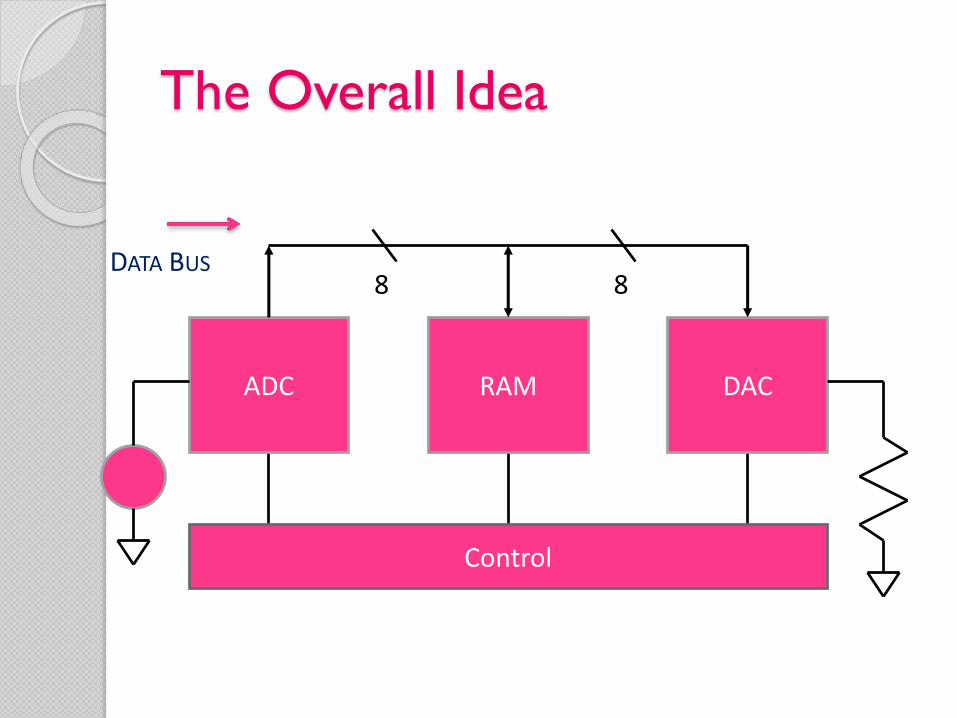
The Overall Idea
13
ADC RAM DAC
Control
8 8DATA BUS

STEP BY STEP
Step 1 Review of ADC and DAC
Step 2 Build the ADC circuit
Step 3 Build the DAC circuit
Step 4 Introduce static RAM
Step 5 Build the on-board clock
Step 6 Introduce control logic and address generator
Step 7 Final changes
14

THE DATA ACQUISITION BOARD
OLD BOARD
15
LED
ADC
DAC
RAMADC Self-Clocking CircuitOn Board clock, control circuitand address generator go here
Choke for data and signal lines
Or resistance array

THE DATA ACQUISITION BOARD
NEW BOARD
16
LED A
rray
Choke for data and signal linesOr resistance array
ADC
ADC Timing Circuit
RAM
DAC
On Board clock, control circuitand address generator go here

STEP 1- REVIEW OF DAC/ADC
A simulation-based exercise
Observe how analog signals are converted to
digital signals
Observe how digital signals are converted to
analog signals
The circuits observed are much simpler than those in
the hardware you will use, but the concepts are
similar
17
STEP 1 PRELAB
Read “Memory devices, timing models, and hierarchical
blocks”, A. Motley, MicroSim Corporation, April 1997
through the “The Supporting Logic” section. The article
can be found in “Useful Articles” Content area on BB Learn
Review ADC, DAC experiments from ECEL 303 Lab III.
Find a box to safely carry around your circuit (6” x 8” x 3”
min).
18
STEP 1 TASKS
Perform calculations, schematic captures, and simulations in Step 1 handout
19

DIGITAL TO ANALOG CONVERSION
Digital signals have discrete levels
MSB - highest weight
LSB - lowest weight
We must convert each N-bit binary value
to a unique analog voltage
20

SIMPLE DAC
21
4-bit counter(not part of DAC)
TTL voltage levels Summing Amplifier
The values of the resistors in the input network of the summing
amplifier determine the “weights” of the digital bits.

SIMPLE DAC
22
V
V
V
VV
U1A
LM324
+3
-2
V+4
V-11
OUT1Vout
R1
80k
R2
40k
R3
20k
R4
10k
D0
D2
D1
D3
D[3-0]S4DSTM1
repeat 32 times
0s 0000
+1ms incr by 0001
endrepeat
VCC+
R5
16k
VCC-
VCC+
V1
15
V2
15
0
VCC-
0
0
The command lines for the 4 bit digital word generator can be added by
double clicking the part and editing the commands as shown
Part number Type Description library
DSTIM1 STIM4 4 bit digital word
generator
Source

ANALOG TO DIGITAL CONVERSION
Note that the 7414 a Schmitt trigger inverter, because of the Schmitt action, it has
different input threshold levels for positive-going (VT+) and negative-going (VT–)
signals, The Schmitt trigger type device translates the slow or noisy edges into
faster and less noisy edges that will meet the input rise and fall specs of the device.
Texas Instrument Application Report SCEA046–September 2011

ADC TYPES
The ADC chip we will use (ADC0804) is based on a
successive approximation (SA) algorithm
The SA Register and Latch (see the functional diagram on
the datasheet, p. 6-6) works like the 74161 counter in our
simulation.
The Ladder and Decoder contains the R-2R network.
The SA converter type is one of the most
commonly used
24

SUCCESSIVE APPROXIMATION ADC
This design requires only a single
comparator.
Analog switches are closed
sequentially by successive
approximation logic producing an
analog output.
The analog output of a high-speed
DAC is compared against the analog
input signal.
The digital result of the comparison is
used to control the contents of a
digital buffer that both drives the
DAC and provides the digital output
word.
25

ADC - INPUT SIDE
26
AnalogInput
VoltageComparator
Invertor
“DAC” signal fromR-2R Network

ADC- INTERNAL VOLTAGE GENERATION
Binary Counter
D-Flip FlopR-2RNetwork

DUAL SLOPE ADCDoes not require a DAC circuit which reduces the complexity
The input signal is applied to an integrator and the counter is reset.
After a pre-determined amount of time (T), a reference voltage having opposite
polarity is applied to the integrator and the counter is reset. At that instant, the
accumulated charge on the integrating capacitor is proportional to the average
value of the input over the interval T.
The integral of the reference is an opposite-going ramp having a slope of VREF/RC.
The counter starts to count.
When the integrator output reaches zero, the count is stopped, and the analog
circuitry is reset.
The charge gained is proportional to VIN × T, and is equal to the amount of charge
lost which is proportional to VREF × tx
The number of counts relative to the full scale count is proportional to tx/T, or
VIN/VREF.
The output of the counter will therefore be a binary representation of the input
voltage.
Conversion accuracy is independent of component values or the clock
frequency.28

DUAL SLOPE ADC
30
TV
Vt
REF
inx
VC

FLASH ENCODING ADC
31Digital Encoding Logic

FLASH ENCODING ADCThe parallel-encoding or flash ADC design provides the fastest
operation at the expense of high component count and high cost.
For an N-bit converter, the circuit employs 2N-1 comparators. A
resistive-divider with 2N resistors provides the reference voltages.
Each comparator produces a 1 when its analog input voltage is higher
than the reference voltage applied to it. Otherwise, the comparator
output is 0. Thus, if the analog input is between VX4 and VX5,
comparators X1 through X4 produce 1s and the remaining comparators
produce 0s.
All comparators with thresholds above the input signal go false while
those below go true. The digital encoding logic converts the result to a
digital number.
32

PIPELINED ADC
33
STAGE I

PRINCIPLE OF OPERATION OF
PIPELINED ADC
The analog VIN, is first sampled, held and applied to the flash ADC in stage 1
which quantizes it to n bits (n=1 to 6 bits).
The output of the first stage ADC is then fed to a DAC (accurate to
about 12 bits), and the analog output is subtracted from the input.
This "residue“ or difference is then fed to the next stage (Stage 2) and
continues through the pipeline, providing n bits per stage until it reaches
the last n-bit flash ADC, which resolves the last n LSB bits.
Because the bits from each stage are determined at different points in time,
all the bits corresponding to the same sample are time-aligned with shift
registers before being fed to a digital-error-correction logic.
34
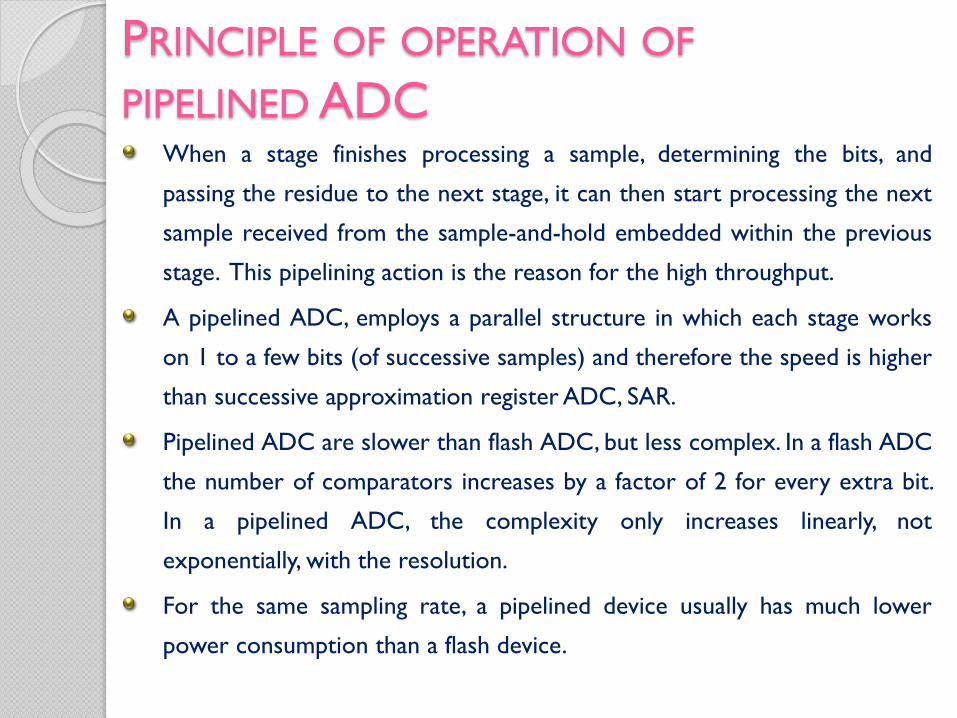
PRINCIPLE OF OPERATION OF
PIPELINED ADCWhen a stage finishes processing a sample, determining the bits, and
passing the residue to the next stage, it can then start processing the next
sample received from the sample-and-hold embedded within the previous
stage. This pipelining action is the reason for the high throughput.
A pipelined ADC, employs a parallel structure in which each stage works
on 1 to a few bits (of successive samples) and therefore the speed is higher
than successive approximation register ADC, SAR.
Pipelined ADC are slower than flash ADC, but less complex. In a flash ADC
the number of comparators increases by a factor of 2 for every extra bit.
In a pipelined ADC, the complexity only increases linearly, not
exponentially, with the resolution.
For the same sampling rate, a pipelined device usually has much lower
power consumption than a flash device.
35

Sigma-Delta ADC
36
One of the more advanced ADC technologies which employs over sampling
and noise shaping
It’s basically a Delta modulator with the components of the transmitter and
receiver rearranged.
1-bit quantizer

SIGMA-DELTA ADC
For a dc input at VIN. The integrator is constantly ramping up or down at node A.
The output of the comparator is fed back through a 1-bit DAC to the summing input at node
B. The DAC is simply a switch that connects a +VREF or –VREF to the negative input of the
difference amplifier. The goal is to maintain the integrator output at zero volts
If the integrator output is positive, the first comparator will output a "high" The switch will be
connected to +VREF, This +VREF feedback signal tends to drive the integrator output in a
negative direction trying to approach zero. If that output voltage ever becomes negative, the
feedback loop will send a corrective signal (-VREF) to the negative input of the integrator to
drive it in a positive direction. The comparator senses a difference (Δ) between the integrator
output and zero volts. The integrator sums (Σ) the comparator's output with the analog input
signal and hence the name Sigma-Delta, ΣΔ. The average dc voltage at node B, output of DAC is
forced to be equal to VIN.
If the analog input is zero volts, the integrator will have no tendency to ramp either positive or
negative, except in response to the feedback voltage. In this scenario, the switch will
continually alternate between +VREF and -VREF , trying to maintain the integrator output at
zero volts.
37
38
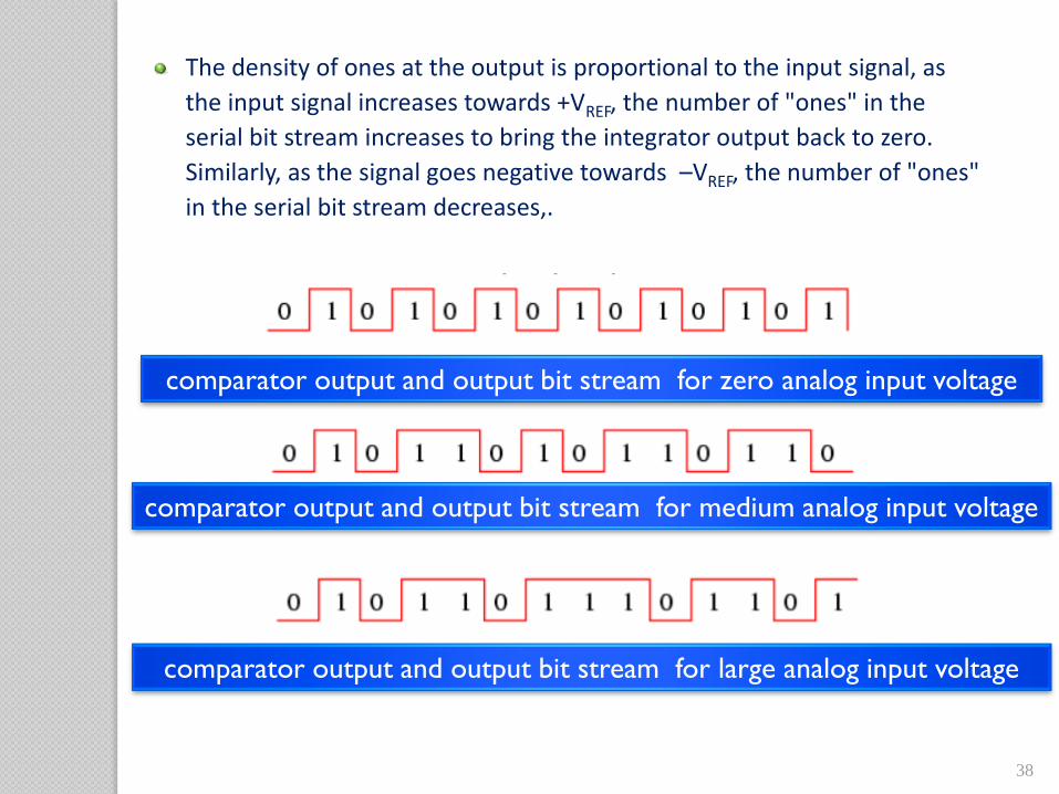
The density of ones at the output is proportional to the input signal, as
the input signal increases towards +VREF, the number of "ones" in the
serial bit stream increases to bring the integrator output back to zero.
Similarly, as the signal goes negative towards –VREF, the number of "ones"
in the serial bit stream decreases,.
comparator output and output bit stream for zero analog input voltage
comparator output and output bit stream for medium analog input voltage
comparator output and output bit stream for large analog input voltage

QUANTIZATION NOISE
The conversion of an analog signal into a digital signal
introduces noise in the signal, which is called
quantization noise. This error is the “round-off” error
that occurs when an analog signal is quantized. If the
resolution of the ADC is q, the quantization noise can be
assumed to be uniformly distributed from −𝑞/2 to
+ 𝑞/2with average quantization noise power of 𝑞2
12
For more details see Article on Sigma Delta converters
39

SIGMA-DELTA ADCThe analysis shows that the average value of the input voltage is
contained in the serial bit stream out of the comparator. The digital filter
and decimator process the serial bit stream and produce the final output
data.
For any given input value in a single sampling interval, the data from the
1-bit ADC is virtually meaningless. Only when a large number of samples
are averaged, will a meaningful value result.
Notice that the integrator which sums the error voltages, minimizes the
quantization noise error and therefore acts as a low-pass filter to the
input signal and a high-pass filter to the quantization noise. Thus, most of
the quantization noise is pushed into higher frequencies. This is known
as noise shaping
Notice also that the sampling rate is higher than the Nyquist rate by
factor of k
40
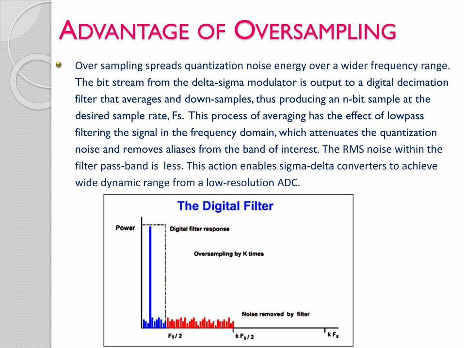
ADVANTAGE OF OVERSAMPLING
Over sampling spreads quantization noise energy over a wider frequency range.
The bit stream from the delta-sigma modulator is output to a digital decimation
filter that averages and down-samples, thus producing an n-bit sample at the
desired sample rate, Fs. This process of averaging has the effect of lowpass
filtering the signal in the frequency domain, which attenuates the quantization
noise and removes aliases from the band of interest. The RMS noise within the
filter pass-band is less. This action enables sigma-delta converters to achieve
wide dynamic range from a low-resolution ADC.
41

NOISE SHAPING
N(s) Represent the quantization noise, to find Y(s)/X(s), assume N(s)=0
1
𝑆𝑋 𝑠 − 𝑌 𝑆 = 𝑌 𝑠 →
𝑌 𝑠
𝑋 𝑠=
1
𝑆+1→ 𝐿𝑃𝐹 𝑓𝑢𝑛𝑐𝑡𝑖𝑜𝑛
to find Y(s)/N(s), assume X(s)=0
𝑁 𝑠 − 𝑌 𝑠1
𝑠= 𝑌(𝑠) →
𝑌 𝑠
𝑁 𝑠=
𝑆
𝑆+1→ 𝐻𝑃𝐹 𝑓𝑢𝑛𝑐𝑡𝑖𝑜𝑛
Therefore the sigma delta modulator acts as a low pass filter function for the signal and a high pass filter function for the quantization noise
The integrator also pre-emphasizes the low frequency components of the signal which helps with practical signals such as voice where low frequency components are important
42Intersil application notes, May 1995 AN9504
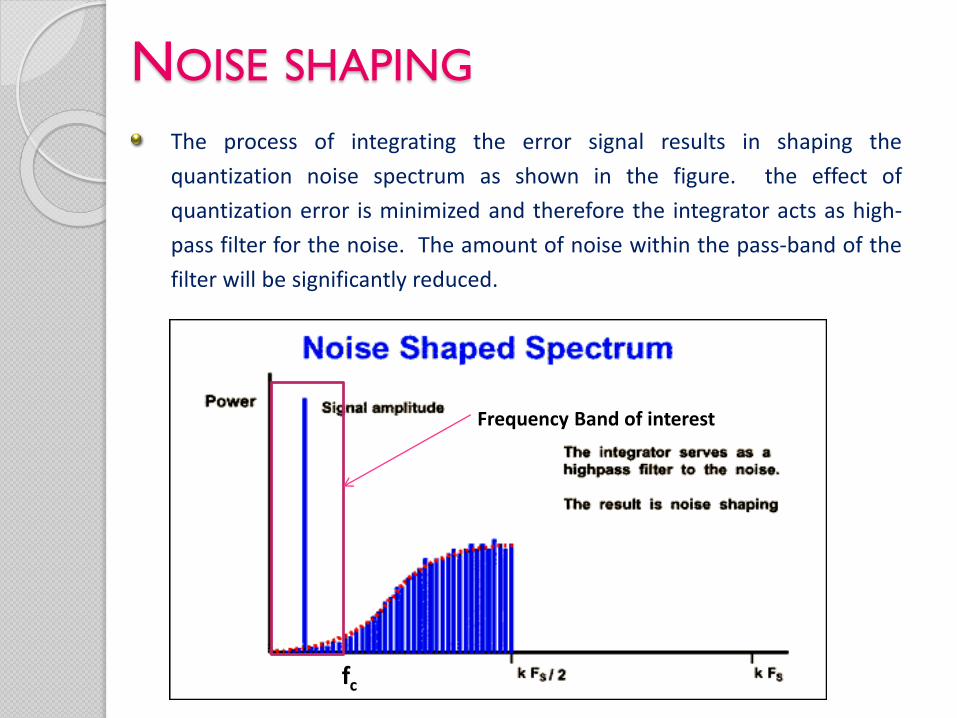
NOISE SHAPING
The process of integrating the error signal results in shaping the
quantization noise spectrum as shown in the figure. the effect of
quantization error is minimized and therefore the integrator acts as high-
pass filter for the noise. The amount of noise within the pass-band of the
filter will be significantly reduced.
43
Frequency Band of interest
fc

OVER SAMPLING IN SIGMA DELTA
ADCOversampling is the process of sampling the input signal at a
much higher rate than the Nyquist frequency to increase the
correlation between successive samples
Increasing the correlation increases the signal-to-noise ratio
(SNR) and the system resolution or effective number of bits
(ENOB).
Therefore effectively, the ΣΔ modulator has a higher number of
bits or higher resolution. An increase in the number of bits by n,
increases the signal to noise ratio by 6𝑛 dB.
As a general guideline, oversampling the ADC by a factor of four
provides one additional bit of resolution, or a 6dB increase in
dynamic range (DR).
44

Resolutions of ADC Types
0 5 10 15 20 25
Successive Approximation
Dual Slope
Sigma-Delta
Flash
Pipeline
Bits
45
Source: Aspects of data acquisition system design, P. Miller, TI Analog Applications, Analog and Mixed-Signal Products, August 1999.

Speeds of ADC Types
1 100 10000 1000000100000000
Successive…
Dual Slope
Sigma-Delta
Flash
Pipeline
Samples per Second
46
Source: Aspects of data acquisition system design, P. Miller, TI Analog Applications, Analog and Mixed-Signal Products, August 1999.
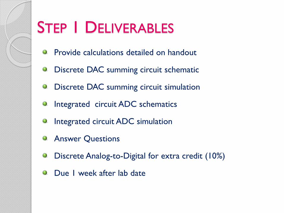
STEP 1 DELIVERABLES
Provide calculations detailed on handout
Discrete DAC summing circuit schematic
Discrete DAC summing circuit simulation
Integrated circuit ADC schematics
Integrated circuit ADC simulation
Answer Questions
Discrete Analog-to-Digital for extra credit (10%)
Due 1 week after lab date
47