PR3BMF51NSLF
1
Sheet No.: OP14009EN
Notice The content of data sheet is subject to change without prior notice.
In the absence of confirmation by device specification sheets, SHARP takes no responsibility for any defects that may occur in equipment using any SHARP
devices shown in catalogs, data books, etc. Contact SHARP in order to obtain the latest device specification sheets before using any SHARP device.
PR3BMF51NSLF Solid State Relay (SSR) is an
integration of an infrared emitting diode (IRED),
a Phototriac Detector and a main output Triac. This
device is ideally suited for controlling high voltage
AC loads with solid state reliability while providing
4kV isolation (Viso(rms)) from input to output.
1. Output current, IT(rms)≤1.2A
2. Non-zero crossing functionary
3. 8 pin DIP package
4. High repetitive peak off-state voltage
(VDRM : 600V)
5. Superior noise immunity (dV/dt : MIN. 100V/μs)
6. Response time, ton : MAX. 100μs
7. High isolation voltage between input and output
(Viso(rms) : 4kV)
8. RoHS directive compliant
1. Approved by UL file No.E94758
(as model No.R3BMF5)
2. Approved by CSA file No.LR63705
(as model No.R3BMF5)
3. Optionary approved by VDE
(DIN EN 60747-5-5), file No.40008898
(as model No.R3BMF5)
4. Package resin : UL flammability grade (94V-0)
1. Isolated interface between high voltage AC devices
and lower voltage DC control circuitry.
2. Switching motors, fans, heaters, solenoids, and
valves.
3. Phase or power control in applications such as
lighting and temperature control equipment.
■Description
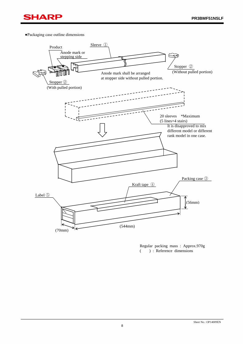
■Features 20 sleeves *Maximum (5 lines×4 stairs)
■Agency approvals/Compliance
■Applications
IT(rms)≦1.2A, Non-Zero Cross type
DIP 8pin Triac output SSR
PR3BMF51NSLF
PR3BMF51NSLF
2
Sheet No.: OP14009EN
UNIT : 1/1 mm
Name R3BMF5 Outline Dimensions
(Business dealing name : PR3BMF51NSLF)
Product mass : Approx. 0.56g
■Pin-Number and internal connection diagram
■Outline
Marking is laser marking
*1) 2-digit number shall be marked according to OLD DIN standard.
*2) Factory identification mark applies to the below.
Without : SUN-S Corporation (Japan)
: SUN-S Electronic Technology (KUNSHAN) Co. Ltd (China)
*3) Business dealing name identification mark : -
Pin material : Copper Alloy
Pin finish : SnCu plating (Cu : TYP. 2%)
①
②
③
④
⑧
⑥
⑤
① : Cathode
② : Anode
③ : Cathode
④ : Cathode
⑤ : Gate
⑥ : T1
⑧ : T2
Rank mark
1.2
±0.3
2.5
4±0
.25
Anode mark
6.5±0.5
Brand name "S"
R3BMF
5
1
Factory identification mark *2
Date Code *1
1.0
5±0
.20
Burr
Max. 0.2
-
Business dealing name identification mark *3
θ
Epoxy resin
7.62±0.30
0.26±0.10
θ
θ:0~13°
0.5±0.1
3.5
±0.5
0.5
TY
P.
9.66±0.50 3
.25
±0.5
0
2.9
±0.5
PR3BMF51NSLF
3
Sheet No.: OP14009EN
■Absolute maximum ratings Ta=25°C
Parameter Symbol Rating Unit
Input Forward current *1 IF 50 mA
Reverse voltage VR 6 V
Output
RMS on-state current *1 IT(rms) 1.2 A
Peak one cycle surge current *2 Isurge 12 A
Repetitive peak off-state voltage VDRM 600 V
Isolation voltage *3 Viso(rms) 4.0 kV
Operating temperature Topr -30 to +85 °C
Storage temperature Tstg -40 to +125 °C
Soldering temperature *4 Tsol 270 °C
*1 The derating factors of absolute maximum rating due to ambient temperature are shown in Fig.1, 2.
*2 50Hz sine wave
*3 AC for 1min, 40 to 60%RH, f=60Hz
*4 For 10s
■Electrical Characteristics Ta=25°C
Parameter Symbol MIN. TYP. MAX. Unit Conditions
Input Forward voltage VF - 1.2 1.4 V IF=20mA
Reverse current IR - - 10 μA VR=3V
Output
Repetitive peak off-state current IDRM - - 100 μA VD=VDRM
On-state voltage VT - - 2.5 V IT=1.2A
Holding current IH - - 25 mA VD=6V
Critical rate of rise of off-state voltage dv/dt 100 - - V/μs VD=(1/√2)· VDRM
Transfer
charac-
teristics
Minimum trigger current IFT - - 10 mA VD=6V, RL=100Ω
Isolation resistance RISO 5×10¹⁰ 1011 - Ω DC500V 40 to 60%RH
Turn on time tON - - 100 μs VD=6V, RL=100Ω,
IF=20mA
PR3BMF51NSLF
4
Sheet No.: OP14009EN
Fo
rwar
d
curr
ent
I F
(m
A)
Ambient temperature Ta (°C)
70
60
50
40
30
20
10
0
-30 -20 -10 0 10 20 30 40 50 60 70 80 90 100
Ambient temperature Ta (°C)
RM
S
on
-sta
te
curr
ent
I T
(rm
s)
(A)
1.0
0.8
0.6
0.4
0.2
0 -30 -20 -10 0 10 20 30 40 50 60 70 80 90 100
1.2
1.4
Fig.1 Forward current vs. ambient temperature(*1)
Fig.2 RMS on-state current vs. ambient temperature(*1)
*1 Mounting conditions
No heat sink
Paper phenol board : 100mm×100mm×1.6mm
All pins should be installed in the print board with soldering.
Whole solder landing dimensions : 140mm2
PR3BMF51NSLF
5
Sheet No.: OP14009EN
■Supplement
●Isolation voltage shall be measured in the following method.
(1) Short between anode and cathode on the primary side and between anode, cathode and gate on the secondary side.
(2) The dielectric withstanding tester with zero-cross circuit shall be used.
(3) The wave form of applied voltage shall be a sine wave.
(It is recommended that the isolation voltage be measured in insulation oil.)
●This Model is approved by UL and CSA.
Approved Model No. : R3BMF5
1. UL file No. : E94758
2. CSA file No. : LR63705
CSA approved mark " " and rating shall be indicated on minimum unit package.
●This product is not designed against irradiation.
This product is assembled with electrical input and output.
This product incorporates non-coherent light emitting diode.
●ODS materials
This product shall not contain the following materials.
Also, the following materials shall not be used in the production process for this product.
Materials for ODS : CFCS, Halon, Carbon tetrachloride, 1.1.1-Trichloroethane (Methyl chloroform)
●Brominated flame retardants
Specified brominated flame retardants (PBB and PBDE) are not used in this device at all.
●Compliance with each regulation
1) The RoHS directive (2002/95/EC)
This product complies with the RoHS directive (2002/95/EC).
Object substances: mercury, lead (except for lead in high melting temperature type solders*1 and glass of
electronic components), cadmium, hexavalent chromium, polybrominated biphenyls (PBB) and polybrominated
diphenyl ethers (PBDE)
*1 : i.e. tin-lead solder alloys containing more than 85% lead 2) Content of six substances specified in Management Methods for Control of Pollution Caused by Electronic
Information Products Regulation (Chinese : 电子信息产品污染控制管理办法).
Category
Toxic and hazardous substances
Lead
(Pb)
Mercury
(Hg)
Cadmium
(Cd)
Hexavalent
chromium
(Cr6+)
Polybrominated
biphenyls
(PBB)
Polybrominated
diphenyl ethers
(PBDE)
Solid State Relay * ✓ ✓ ✓ ✓ ✓
✓ : indicates that the content of the toxic and hazardous substance in all the homogeneous materials of the part is
below the concentration limit requirement as described in SJ/T 11363-2006 standard.
* : indicates that the content of the toxic and hazardous substance in at least one homogeneous material of the part
exceeds the concentration limit requirement as described in SJ/T 11363-2006 standard.
Lead in high melting temperature type solders (i.e. tin-lead solder alloys containing more than 85% lead) and glass of
electronic components (designated by “*” in the above table) are exempt from the RoHS directive (2002/95/EC),
because there is no effective way to eliminate or substitute them by present scientific technology.
PR3BMF51NSLF
6
Sheet No.: OP14009EN
■Notes
●Circuit designing
(1) Trigger current
The LED used in the Solid state relay generally decreases the light emission power by operation.
In case of long operation time, please decide IF value so that IF is twice or more of the Maximum value
of the Minimum triggering current at circuit design with considering the decreases of the light emission power
of the LED. (50%/5years)
(2) Snubber circuit
This device doesn’t have built-in snubber circuit.
To avoid the false operation and protect SSR, please locate the appropriate snubber circuit between output pins
base by the load. (Recommendable values : Rs=47Ω, Cs=0.022μF)
Particularly, in case the device is used for the load such as solenoid valves and motors, false operation may
happen in off-state due to rapid change of voltage at output pins caused by the phase difference of load current.
So please be sure to locate the snubber circuit (Rs=47Ω, Cs=0.022μF) and make sure the device works properly
in actual conditions.
In addition, the values of snubber circuit may have to be changed if necessary after tested in actual conditions.
(3) Off-state input current
Input current (IF) at off-state shall be set 0.1mA or less.
(4) Pulse drive
In case that pulse drive is carried out, the pulse width of input signal should be 1ms or more.
(5) If the voltage exceeding the repetitive peak off-state voltage (VDRM) in the absolute maximum ratings is applied
to the phototriac, it may cause not only faulty operation but breakdown.
Make sure that the surge voltage exceeding VDRM shall not be applied by using the varistor, CR.
●Cleaning
(1) Solvent cleaning : Solvent temperature 45°C or less Immersion for 3 min or less
(2) Ultrasonic cleaning : The effect to device by ultrasonic cleaning differs by cleaning bath size, ultrasonic power
output, cleaning time, PCB size or device mounting condition etc.
Please test it in actual using condition and confirm that any defect doesn't occur
before starting the ultrasonic cleaning.
(3) Applicable solvent : Ethyl alcohol, Methyl alcohol, Isopropyl alcohol
In case the other solvent is used, there are cases that the packaging resin is eroded.
Please use the other solvent after thorough confirmation is performed in actual using condition.
●Using method
As to this product, all pin shall be used by soldering on the print wiring board. (Socket and others shall not be used.)
●Precautions for Soldering
(1) In case of flow soldering (Avoid immersing the resin part in the solder.)
It is recommended that flow soldering be carried out at 270°C or less and within 10s
(Pre-heating:100 to 150°C, 30 to 80s) : Within 2 times
(2) In case of hand soldering
It is recommended that hand soldering be carried out at 400°C or less and within 3s: Within 2 times
(3) Other precautions
Depending on equipment and soldering conditions (temperature, Using solder etc.),
the effect to junction between PCB and lead pins of the device is different.
Please confirm that there is no problem on the actual use conditions
PR3BMF51NSLF
7
Sheet No.: OP14009EN
■Package specification
●Package materials
No. Name Materials Purposes
① Sleeve HIPS or ABS with preventing
static electricity Products packaged
② Stopper Styrene-Elastomer Products fixed
③ Packing case Corrugated cardboard Sleeve packaged
④ Kraft tape Paper Lid of packaged case fixed
⑤ Label Paper
Model No. (Business dealing name), Lot No.
Quantity, Country of origin, Company name
and Inspection date specified
●Package method
(1) MAX. 50pcs. of products shall be packaged in a sleeve ① and both of sleeve edges shall be fixed by stoppers ②.
(2) MAX. 20 sleeves (Product : 1000pcs) above shall be packaged in a packing case ③.
(3) The label ⑤ shall be put on the side of the packing case.
(4) Case shall be closed with the lid and enclosed with kraft tape ④.
●Sleeve outline dimensions
Note 1) Thickness : 0.5±0.2mm
2) Process with applying antistatic treatment. 3) Unless otherwise specified tolerances shall be ±0.5mm.
(However except for deformation due to the rubber stopper in sleeve.)
(Unit : mm)
12 1
0.8
5.8
6.7
520±2
8-R0.5
PR3BMF51NSLF
8
Sheet No.: OP14009EN
Regular packing mass : Approx.970g
( ) : Reference dimensions
20 sleeves *Maximum
(5 lines×4 stairs)
It is disapproved to mix
different model or different
rank model in one case.
Kraft tape ④
Label ⑤
Packing case ③
●Packaging case outline dimensions
(70mm) (544mm)
(56mm)
Sleeve ① Product
Anode mark or stepping side
Stopper ②
(With pulled portion)
Anode mark shall be arranged
at stopper side without pulled portion.
Stopper ②
(Without pulled portion)
PR3BMF51NSLF
9
Sheet No.: OP14009EN
(Attachment-1-1)
●This specification shall be applied to Solid State Relay (SSR), Model No. R3BMF5 series as an option.
●Applicable Models (Business dealing name)
PR3BMF51YSLF
●The relevant models are the models Approved by VDE according to DIN EN 60747-5-5
VDE approved No. : 40008898
Approved Model No. : R3BMF5
・Operating isolation voltage VIORM (Peak) : 890V
・Transient voltage (Peak) : 7100V
・Pollution : 2
・Clearances distance (Between input and output) : 6.4mm (MIN.)
・Creepage distance (Between input and output) : 6.4mm (MIN.)
・Isolation thickness between input and output : 0.15mm (MIN.)
・Tracking-proof : CTI 175
・Safety limit values Current (Isi) : 200mA (Diode side)
Power (Psi) : 3600mW (Triac side)
Temperature (Tsi) : 150°C
In order to keep safety electric isolation of photocoupler, please set the protective circuit to keep within safety
limit values when the actual application equipment troubled.
・Indication of VDE approval " " is printed on minimum unit package.
●Outline Refer to the attachment-1-2.
●Isolation specification according to EN 60747-5-5
Parameter Symbol Condition Rating Unit Remark
Class of environmental test - - 30/100/21 -
Pollution - - 2 -
Maximum operating isolation voltage VIORM(PEAK) - 890 V
Refer to
the Diagram 1, 2
(Attachement-1-3)
Partial discharge test voltage (Between input and output)
Diagram 1
Vm(PEAK)
tm=10s,
qc<5pC 1340 V
Diagram 2 tst1=1s,
qc<5pC 1670 V
Maximum over-voltage Vini,a(PEAK) tini=60s 7100 V
Safety maximum ratings
Refer to
the Fig. 3, 4
(Attachement-1-3)
1) Case temperature Tsi IF=0,
PC=0 150 °C
2) Input current Isi PC=0 200 mA
3) Electric power (Output or Total power dissipation) Psi - 3600 mW
Isolation resistance
(Test voltage between input and output ; DC500V)
RISO
Tamb=Tsi MIN. 109
Ω Tamb=Topr
(MAX) MIN. 1011
Tamb=25°C MIN. 1012
●Precautions in performing isolation test
1) Partial discharge test methods shall be the ones according to the specifications of EN 60747-5-5.
2) Please don't carry out isolation test (Viso) over Vini,a.
This product deteriorates isolation characteristics by partial discharge due to applying high voltage (ex. Vini,a).
And there is possibility that partial discharge occurs in operating isolation voltage (VIORM).
V DE
PR3BMF51NSLF
10
Sheet No.: OP14009EN
Product mass : Approx. 0.56g
UNIT : 1/1 mm
Name R3BMF5 Outline Dimensions
(Business dealing name : PR3BMF51YSLF)
(Attachment-1-2)
●Pin-Number and internal connection diagram
●Outline
Marking is laser marking
*1) 2-digit number shall be marked according to OLD DIN standard.
*2) Factory identification mark applies to the below.
Without : SUN-S Corporation (Japan)
: SUN-S Electronic Technology (KUNSHAN) Co. Ltd (China)
*3) Pin material : Copper Alloy
Pin finish : SnCu plating (Cu : TYP. 2%)
θ
Epoxy resin
θ
θ:0~13°
7.62±0.30
0.26±0.10
0.5
TY
P.
9.66±0.50
2.9
±0.5
0.5±0.1
3.2
5±0
.50
3
.5±0
.5
①
②
③
④
⑧
⑥
⑤
① : Cathode
② : Anode
③ : Cathode
④ : Cathode
⑤ : Gate
⑥ : T1
⑧ : T2
VDE identification mark
4
Anode mark
6.5±0.5 Rank mark
Brand name "S"
R3
BMF5
1
Factory identification mark *2
Date code *1
1.0
5±0
.20
Burr
Max. 0.2
①
②
③
④
⑧
⑥
⑤
1.2
±0.3
2.5
4±0
.25
“L” identification mark
-
PR3BMF51NSLF
11
Sheet No.: OP14009EN
(Fig.3) Safety maximum power dissipation
vs. ambient temperature
(When failed)
Ambient temperature Ta (°C)
0 25 50 75 100 125 150 0
1000
2000
3600
3000
4000
Saf
ety
max
imu
m f
orw
ard
cu
rren
t
Isi
(mA
)
(Fig.4) Safety maximum forward current
vs. ambient temperature
(When failed)
0 0
25 50 75 100 125 150
50
100
150
200
250
Saf
ety
max
imu
m p
ow
er d
issi
pat
ion
Psi
(m
W)
Ambient temperature Ta (°C)
(Attachment-1-3)
Method of Diagram 1: Breakdown test (Apply to type test and sampling test)
Method of Diagram 2: Non breakdown test (Apply to all device test)
PR3BMF51NSLF
12
Sheet No.: OP14009EN
■Important Notices · The circuit application examples in this publication are
provided to explain representative applications of SHARP
devices and are not intended to guarantee any circuit design or
license any intellectual property rights. SHARP takes no
responsibility for any problems related to any intellectual
property right of a third party resulting from the use of SHARP's
devices.
· Contact SHARP in order to obtain the latest device specification
sheets before using any SHARP device. SHARP reserves the
right to make changes in the specifications, characteristics, data,
materials, structure, and other contents described herein at any
time without notice in order to improve design or reliability.
Manufacturing locations are also subject to change without
notice.
· Observe the following points when using any devices in this
publication. SHARP takes no responsibility for damage caused
by improper use of the devices which does not meet the
conditions and absolute maximum ratings to be used specified in
the relevant specification sheet nor meet the following
conditions:
(i) The devices in this publication are designed for use in general
electronic equipment designs such as:
--- Personal computers
--- Office automation equipment
--- Telecommunication equipment [terminal]
--- Test and measurement equipment
--- Industrial control
--- Audio visual equipment
--- Consumer electronics
(ii) Measures such as fail-safe function and redundant design
should be taken to ensure reliability and safety when SHARP
devices are used for or in connection
with equipment that requires higher reliability such as:
--- Transportation control and safety equipment (i.e.,
aircraft, trains, automobiles, etc.)
--- Traffic signals
--- Gas leakage sensor breakers
--- Alarm equipment
--- Various safety devices, etc.
(iii) SHARP devices shall not be used for or in connection with
equipment that requires an extremely high level of reliability and
safety such as:
--- Space applications
--- Telecommunication equipment [trunk lines]
--- Nuclear power control equipment
--- Medical and other life support equipment (e.g.,
scuba).
· If the SHARP devices listed in this publication fall within the
scope of strategic products described in the Foreign Exchange
and Foreign Trade Law of Japan, it is necessary to obtain
approval to export such SHARP devices.
· This publication is the proprietary product of SHARP and is
copyrighted, with all rights reserved. Under the copyright laws,
no part of this publication may be reproduced or transmitted in
any form or by any means, electronic or mechanical, for any
purpose, in whole or in part, without the express written
permission of SHARP. Express written permission is also
required before any use of this publication may be made by a
third party.
· Contact and consult with a SHARP representative if there are
any questions about the contents of this publication.