160
Copyright by Anil Prabhakar 2015

Copyright
by
Anil Prabhakar
2015

The Report Committee for Anil PrabhakarCertifies that this is the approved version of the following report:
Design and Prototype of an All Digital System for
Baseband FM Multiplex Signal Demodulation
APPROVED BY
SUPERVISING COMMITTEE:
Jacob Abraham, Supervisor
Shiva Akkihal

Design and Prototype of an All Digital System for
Baseband FM Multiplex Signal Demodulation
by
Anil Prabhakar, B.S.E.E.
REPORT
Presented to the Faculty of the Graduate School of
The University of Texas at Austin
in Partial Fulfillment
of the Requirements
for the Degree of
Master of Science in Engineering
THE UNIVERSITY OF TEXAS AT AUSTIN
May 2015

Dedicated to my wife Magaly, my parents Rao and Rathna, and my brother
Rajesh.
Acknowledgments
First and foremost, I would like to thank all of my family for their love
and support. Without their constant encouragement and patience, I would
not have made it through this program. Thank you for always reminding me
of what is important in this life; for having faith in me; and for providing
encouragement when most needed.
I would also like to thank all of my professors, classmates, and coworkers
who taught me along the way; with a very special thank you to Professor
Jacob Abraham and Dr. Shiva Akkihal, both of whom guided me through
this Master’s Report. I have learned much from all of you and am a better
engineer because of it.
v

Design and Prototype of an All Digital System for
Baseband FM Multiplex Signal Demodulation
Anil Prabhakar, M.S.E
The University of Texas at Austin, 2015
Supervisor: Jacob Abraham
The continuing increase in transistor densities and operation frequen-
cies of digital circuits is leading to the replacement of many analog circuits
by their digital circuit counterparts. This trend can be attributed to the flex-
ibility and robustness provided by digital circuits over analog circuits. One
application in which digital circuits are replacing analog circuits is in the mod-
ulation and demodulation of baseband frequency modulated (FM) radio sig-
nals. In this project, an all digital system for demodulating baseband FM
Multiplex (MPX) signals is simulated, designed, and prototyped on a Xilinx
Spartan-3AN FPGA. The design architecture is simulated using Scilab nu-
merical computation software; implemented in Verilog Hardware Description
Language; and tested using the digital to analog converters (DACs) on the
Xilinx Spartan-3AN Starter Kit. The oscilloscope images at the end of this
report show that the implemented system can successfully demodulate the
19kHz pilot tone, left channel signal, and right channel signal of a digitized
FM MPX modulated signal sampled at 192kHz.
vi

Table of Contents
Acknowledgments v
Abstract vi
List of Tables ix
List of Figures x
Chapter 1. Introduction 1
1.1 Project Description . . . . . . . . . . . . . . . . . . . . . . . . 3
1.2 FM MPX Basics . . . . . . . . . . . . . . . . . . . . . . . . . . 4
1.2.1 History of the FM MPX Signal . . . . . . . . . . . . . . 5
1.2.2 FM MPX Baseband Spectrum . . . . . . . . . . . . . . 6
1.2.3 FM MPX Baseband Modulator and Demodulator . . . . 7
1.2.4 FM MPX Signal Implemented in FM MPX Modulator LUT 9
1.3 Organization of the Report . . . . . . . . . . . . . . . . . . . . 11
Chapter 2. FM MPX Modulator and Demodulator Architec-ture and Simulation 13
2.1 Digital Filter Architecture and Simulation . . . . . . . . . . . 16
2.1.1 Comparison of Digital Filter Topologies . . . . . . . . . 16
2.1.2 FIR Filter Basics . . . . . . . . . . . . . . . . . . . . . . 17
2.1.3 FIR Filter Design and Simulation for FM MPX Demod-ulator . . . . . . . . . . . . . . . . . . . . . . . . . . . . 30
2.1.3.1 Design of 19kHz BPF . . . . . . . . . . . . . . . 31
2.1.3.2 Design of 38kHz BPF . . . . . . . . . . . . . . . 34
2.1.3.3 Design of 15kHz LPF . . . . . . . . . . . . . . . 37
2.1.3.4 Simulations with Designed Filters . . . . . . . . 40
2.1.3.5 Re-Design of the 19kHz BPF . . . . . . . . . . 45
vii

2.1.4 Finalized FIR Filter Design from High Level Simulations 48
2.2 Frequency Doubler Architecture . . . . . . . . . . . . . . . . . 50
2.2.1 All Digital Phase Locked Loop (ADPLL) Basics . . . . 51
2.2.1.1 Phase Detector . . . . . . . . . . . . . . . . . . 55
2.2.1.2 Loop Filter . . . . . . . . . . . . . . . . . . . . 57
2.2.1.3 Numerically Controlled Oscillator (NCO) . . . . 60
2.2.2 Design of Frequency Doubler Architecture . . . . . . . . 68
2.2.2.1 Phase Detector and Loop Filter Simulations . . 68
2.2.2.2 NCO Architecture . . . . . . . . . . . . . . . . 74
2.2.2.3 Amplifier A Architecture . . . . . . . . . . . . . 77
2.2.2.4 Complete Frequency Doubler ADPLL Architecture 81
2.3 Complete Modulator and Demodulator System Simulation . . 85
Chapter 3. Implementation on Xilinx Spartan-3AN FPGA 92
3.1 Clock Scheme . . . . . . . . . . . . . . . . . . . . . . . . . . . 95
3.2 Reset Scheme . . . . . . . . . . . . . . . . . . . . . . . . . . . 96
3.3 Module Descriptions . . . . . . . . . . . . . . . . . . . . . . . 97
3.3.1 Sub-Module: clk div 10 . . . . . . . . . . . . . . . . . . 99
3.3.2 Sub-Module: debounce . . . . . . . . . . . . . . . . . . 100
3.3.3 Sub-Module: dcm1 . . . . . . . . . . . . . . . . . . . . . 101
3.3.4 Sub-Module: clk div 512 . . . . . . . . . . . . . . . . . 102
3.3.5 Sub-Module: mpx encoder . . . . . . . . . . . . . . . . 103
3.3.6 Sub-Module: mpx decoder . . . . . . . . . . . . . . . . 105
3.3.7 Sub-Module: spi top . . . . . . . . . . . . . . . . . . . . 112
3.3.8 Sub-Module: spi controller mpx enc . . . . . . . . . . . 118
3.4 FPGA Resource Utilization . . . . . . . . . . . . . . . . . . . . 124
Chapter 4. System Validation 125
4.1 Validation of SPI, MPX Encoder, and 19kHz BPF . . . . . . . 126
4.2 Validation of Frequency Doubler . . . . . . . . . . . . . . . . . 130
4.3 Validation of Complete System . . . . . . . . . . . . . . . . . . 133
Chapter 5. Conclusion 141
Bibliography 145
viii

List of Tables
2.1 Comparison of IIR and FIR Filter Characteristics . . . . . . . 17
2.2 FM MPX Demodulator FIR Filter Designs Based on High-LevelSimulations . . . . . . . . . . . . . . . . . . . . . . . . . . . . 50
2.3 Comparison of Expected and Loop Filter Simulation vd n Values 73
ix

List of Figures
1.1 Overall System Block Diagram . . . . . . . . . . . . . . . . . . 4
1.2 FM MPX Spectrum and Modulation Levels . . . . . . . . . . 7
1.3 FM MPX Modulator Conceptual Block Diagram . . . . . . . . 8
1.4 FM MPX Demodulator Conceptual Block Diagram . . . . . . 9
2.1 Direct Form FIR Filter Conceptual Block Diagram . . . . . . 18
2.2 Passband, Stopband, and Transition Band for a Low Pass Filter 19
2.3 Generalized Impulse Response of a Filter . . . . . . . . . . . . 22
2.4 Ideal LPF Frequency (left) and Impulse (right) Responses . . 23
2.5 Implementable LPF Impulse Response for N =20 and ft=0.23.Weights w(n) are Equivalent to Coefficients bi for n=i=0,1,2,...,N. 25
2.6 Effects of sinc Function Truncation on Frequency Response . . 26
2.7 Multiplying sinc Function Coefficients with Window Weightsfor Obtaining Final “Windowed” FIR Filter Coefficient Values 28
2.8 Effects of Rectangular and Hamming Windows on LPF Fre-quency Response . . . . . . . . . . . . . . . . . . . . . . . . . 28
2.9 19kHz BPF Frequency Response Specification . . . . . . . . . 32
2.10 19kHz BPF Coefficients for N=384 . . . . . . . . . . . . . . . 33
2.11 Frequency Response of Designed 19kHz BPF with N=384 . . . 34
2.12 38kHz BPF Frequency Response Specification . . . . . . . . . 35
2.13 38kHz BPF Coefficients for N=384 . . . . . . . . . . . . . . . 36
2.14 Frequency Response of Designed 38kHz BPF with N=384 . . . 37
2.15 15kHz LPFs Frequency Response Specification . . . . . . . . . 38
2.16 15kHz LPF Coefficients for N=384 . . . . . . . . . . . . . . . 39
2.17 Frequency Response of Designed 15kHz LPFs with N=384 . . 40
2.18 Scilab Model for System-Level Simulations . . . . . . . . . . . 41
2.19 Comparison of Modulated (top) and Demodulated (bottom)Left Channel Signals with Initial FIR Filter Designs . . . . . . 42
x

2.20 Comparison of Modulated (top) and Demodulated (bottom)Right Channel Signals with Initial FIR Filter Designs . . . . . 42
2.21 Comparison of Equivalent Modulated (top) and Demodulated(bottom) Signals Relating to the Designed 38kHz BPF: SignalsHave Identical Phase . . . . . . . . . . . . . . . . . . . . . . . 43
2.22 Comparison of Equivalent Modulated (top) and Demodulated(bottom) Signals Relating to the Designed 15kHz LPF: SignalsHave Identical Phase . . . . . . . . . . . . . . . . . . . . . . . 44
2.23 Comparison of Equivalent Modulated (top) and Demodulated(bottom) Signals Relating to the Designed 19kHz BPF: SignalsHave Phase Shift of 5.3µs (i.e. 5.6636 radians) . . . . . . . . . 44
2.24 19kHz BPF Coefficients for N=442 . . . . . . . . . . . . . . . 47
2.25 Frequency Response of Designed 19kHz BPF with N=442 . . . 47
2.26 Comparison of Equivalent Modulated (top) and Demodulated(bottom) Signals Relating to the Designed 19kHz BPF withN=442: Signals Have Phase Shift of 1.75µs (i.e. 0.20295 radians) 48
2.27 Comparison of Modulated (top) and Demodulated (bottom)Left Channel Signals with Re-Designed 19kHz BPF . . . . . . 49
2.28 Comparison of Modulated (top) and Demodulated (bottom)Right Channel Signals with Re-Designed 19kHz BPF . . . . . 49
2.29 Conceptual Block Diagram of the Chosen ADPLL Topology . 52
2.30 Multiplier Phase Detector . . . . . . . . . . . . . . . . . . . . 55
2.31 IIR Filter Conceptual Block Diagram . . . . . . . . . . . . . . 58
2.32 NCO Architecture . . . . . . . . . . . . . . . . . . . . . . . . 61
2.33 Representation of Phase Accumulator as Digital Phase Wheel 62
2.34 Block Diagram of Typical NCO Implementation . . . . . . . . 65
2.35 Block Diagram of Frequency-Tunable and Phase-Tunable NCOfor use with ADPLLs . . . . . . . . . . . . . . . . . . . . . . . 67
2.36 Scilab Model for Phase Detector and Loop Filter Simulations . 69
2.37 Loop Filter 1 Block Diagram . . . . . . . . . . . . . . . . . . . 71
2.38 Loop Filter 1 Simulation Results: vd n vs. ( θ1 − θ2) . . . . . . 71
2.39 Loop Filter 2 Block Diagram . . . . . . . . . . . . . . . . . . . 72
2.40 Loop Filter 2 Simulation Results: vd n vs. (θ1 − θ2) . . . . . . 73
2.41 NCO Architecture for the Frequency Doubler Block U(X,Y) areunsigned fixed-point signals with X integer and Y fractionalbits A(P,Q) are signed fixed-point signals with P integer andQ fractional bits . . . . . . . . . . . . . . . . . . . . . . . . . 75
xi

2.42 Linear Approximation of Loop Filter vd n vs. θdiff . . . . . . 79
2.43 Conceptual Frequency Doubler ADPLL Block Diagram for thisProject . . . . . . . . . . . . . . . . . . . . . . . . . . . . . . . 81
2.44 Complete Frequency Doubler Architecture . . . . . . . . . . . 82
2.45 Flow Chart for Strobing and Processing of vd n Values in theFrequency Doubler Block . . . . . . . . . . . . . . . . . . . . . 84
2.46 vd n Transition Time for a θdiff Transition from -90° to 0° . . 85
2.47 Scilab mpx modulator Model for System-Level Simulations . . 87
2.48 Scilab Frequency Doubler Model for System-Level Simulations 88
2.49 MPX Out Signal Generated by mpx modulator Scilab Model . 89
2.50 FFT of MPX Out Signal Showing Frequency Components andModulation Levels . . . . . . . . . . . . . . . . . . . . . . . . 89
2.51 Comparison of Modulated (top) and Demodulated (bottom)19kHz Pilot Tone . . . . . . . . . . . . . . . . . . . . . . . . . 90
2.52 Comparison of Modulated (top) and Demodulated (bottom)Left Channel Signals . . . . . . . . . . . . . . . . . . . . . . . 91
2.53 Comparison of Modulated (top) and Demodulated (bottom)Right Channel Signals . . . . . . . . . . . . . . . . . . . . . . 91
3.1 Top Level Module Implemented on the Xilinx Spartan-3AN FPGA 94
3.2 Sub-Modules of the Top-Level FPGA Design . . . . . . . . . . 98
3.3 Top-Level Diagram of clk div 10 Sub-Module . . . . . . . . . . 99
3.4 Top-Level Diagram of debounce Sub-Module . . . . . . . . . . 100
3.5 Top-Level Diagram of dcm1 Sub-Module . . . . . . . . . . . . 101
3.6 Top-Level Diagram of clk div 512 Sub-Module . . . . . . . . . 103
3.7 Top-Level Diagram of mpx encoder Sub-Module . . . . . . . . 104
3.8 Internal Block Diagram of mpx encoder Sub-Module . . . . . . 105
3.9 Top-Level Diagram of mpx decoder Sub-Module . . . . . . . . 106
3.10 Internal Block Diagram of Final Circuit for mpx decoder Sub-Module . . . . . . . . . . . . . . . . . . . . . . . . . . . . . . . 107
3.11 Pipeline Schedule for mpx decoder Sub-Module . . . . . . . . . 108
3.12 FIR Implementation on FPGA . . . . . . . . . . . . . . . . . 109
3.13 Final Implementation Details for 19kHz FIR BPF . . . . . . . 110
3.14 Final Implementation Details for 38kHz FIR BPF . . . . . . . 111
3.15 Final Implementation Details for 15kHz FIR LPF . . . . . . . 112
xii

3.16 Top-Level Diagram of spi top Sub-Module . . . . . . . . . . . 113
3.17 SPI Configuration of one Master with Multiple Slaves . . . . . 114
3.18 SPI Connections Between FPGA and DAC . . . . . . . . . . . 115
3.19 SPI Data Transfer Waveforms for FPGA Write to DAC . . . . 116
3.20 DAC 24-bit Protocol . . . . . . . . . . . . . . . . . . . . . . . 116
3.21 DAC Command and Address Nibbles Decoding . . . . . . . . 117
3.22 Top-Level Diagram of spi controller mpx enc Sub-Module . . . 119
3.23 FSM Implemented by the spi controller mpx enc Sub-Module 123
3.24 FPGA Resource Utilization for Final Implemented Design . . 124
4.1 Yellow Waveform: MPX Out Signal Generated by mpx encoderSub-Module . . . . . . . . . . . . . . . . . . . . . . . . . . . . 128
4.2 MPX Out Signal from Scilab Simulations . . . . . . . . . . . . 128
4.3 Frequency Comparison of Generated 19kHz Pilot Tone (GreenWaveform) with Recovered 19kHz Pilot Tone (Blue Waveform) 129
4.4 Measured Phase Difference Between Generated 19kHz Pilot Tone(Green Waveform) and Recovered 19kHz Pilot Tone (Blue Wave-form) . . . . . . . . . . . . . . . . . . . . . . . . . . . . . . . . 130
4.5 Frequency and Phase Comparison of Generated 19kHz PilotTone (Green Waveform), Full Scale 19kHz Pilot Tone (BlueWaveform), and Frequency Doubled 38kHz Signal (Yellow Wave-form) . . . . . . . . . . . . . . . . . . . . . . . . . . . . . . . . 132
4.6 Zoomed View: Frequency and Phase Comparison of Generated19kHz Pilot Tone (Green Waveform), Full Scale 19kHz PilotTone (Blue Waveform), and Frequency Doubled 38kHz Signal(Yellow Waveform) . . . . . . . . . . . . . . . . . . . . . . . . 132
4.7 Required Synchronization of sum x 0p5 and diff x 0p5 Signalsfor Proper Left and Right Channel Demodulation . . . . . . . 136
4.8 Relative Phase of sum x 0p5 and diff x 0p5 Signals from Be-havioral Simulations with All FIR Filters of Order N =442 . . 137
4.9 Oscilloscope Screen Shot of Full-Scale Recovered 19kHz PilotTone (Yellow Waveform), Demodulated 5kHz Left Channel (BlueWaveform), and Demodulated 7kHz Right Channel (Green Wave-form) . . . . . . . . . . . . . . . . . . . . . . . . . . . . . . . . 139
4.10 Zoomed View of Oscilloscope Screen Shot of Full-Scale Recov-ered 19kHz Pilot Tone (Yellow Waveform), Demodulated 5kHzLeft Channel (Blue Waveform), and Demodulated 7kHz RightChannel (Green Waveform) . . . . . . . . . . . . . . . . . . . 140
xiii

Chapter 1
Introduction
The replacement of analog circuits by their digital circuit counterparts
is becoming more prevalent as a result of the continuing increase of transis-
tor densities and operating frequencies of digital circuits. The motivation for
this switch can largely be attributed to the flexibility and robustness pro-
vided by digital circuits over analog circuits [3]. For example, digital circuits
are less susceptible to PVT (process, voltage, and temperature) variations,
electrical noise, and component aging than analog circuits. Furthermore, re-
programmable digital integrated circuits such as Field Programmable Gate
Arrays (FPGAs) provide the flexibility to design circuits that implement com-
pletely different functions and algorithms. This re-programmability allows the
same integrated circuit to be adapted to different standards and also facilitates
the fixing of any errors that may exist in the circuit [3].
Radio signal reception is one of the many applications in which digital
circuits are replacing analog circuits. This switch to digital circuits is lead-
ing to the invention of new digital communication systems in which the radio
frequency (RF) signal is sampled and demodulated with as little analog ma-
nipulation as possible. Ideally, in a digital radio receiver system, an analog
1

to digital converter (ADC) would be connected directly to the receiving an-
tenna to convert the RF signal to a digital signal [3]. Thus, the remainder of
the signal processing can be accomplished in the digital domain. In practice,
though, the ADCs that are sufficiently fast to directly digitize the RF signal
are prohibitively expensive [3]. Therefore, analog circuitry is still used in the
front-end circuitry that down-converts the high frequency RF signal to a lower,
intermediate frequency (IF) signal that can be digitized. This IF signal can
subsequently be digitally processed to extract the baseband signal, which, in
turn, can also be demodulated digitally.
The goal of the work presented in this report is to simulate, design, and
prototype a digital system for demodulating FM MPX (Frequency Modulated
Multiplexed) baseband signals. Scilab, an open source numerical computation
program, was used for the architectural simulations of the digital modulator
and demodulator. The design implementation and prototype were accom-
plished using the Xilinx Spartan-3AN Starter Kit platform and the Xilinx ISE
Design Suite software. Verilog Hardware Description Language was used for
the design implementation. The correct functionality of the demodulator sys-
tem was confirmed by using the digital to analog converters (DACs) on the
Starter Kit to bring out the demodulated signals to probe points that could
be accessed with an oscilloscope. Finally, the signals captured by the oscillo-
scope were compared with the original modulated signals to ensure that the
demodulator correctly recovered them from the multiplexed baseband signal.
This chapter will focus on the overall project description and the ba-
2

sics of FM MPX signal modulation and demodulation. An overview of the
remainder of the report will be presented at the end of this chapter.
1.1 Project Description
Figure 1.1 shows the overall system block diagram for this project. The
following three main blocks are implemented on the FPGA:
1. FM MPX Modulator Look Up Table (LUT): this LUT contains the val-
ues of a modulated baseband FM MPX signal sampled at 192kHz. De-
tails of the modulated FM MPX signal contained in this LUT will be
discussed in section 1.2.4.
2. FM MPX Demodulator: this block receives the modulated FM MPX
signal from the FM MPX Modulator LUT and extracts the 19kHz pi-
lot tone, left channel signal L(t), and right channel signal R(t). These
demodulated signals are subsequently sent to the SPI Core block.
3. SPI Core: this block implements a Serial Peripheral Interface (SPI) that
allows the FPGA to route signals to the on-board digital to analog con-
verter (DAC). The SPI Core block receives the demodulated signals from
the FM MPX Demodulator and routes them to three distinct channels
of the DAC.
The DAC on the Starter Kit converts the digital signals it receives
from the SPI Core into analog signals. These analog signals are monitored
3

using an oscilloscope to ensure that the FM MPX Demodulator is properly
demodulating the left channel, right channel, and pilot tone signals.
Figure 1.1: Overall System Block Diagram
1.2 FM MPX Basics
This section begins with a brief history of the FM MPX signal. In
continuation, the FM MPX Baseband Spectrum is discussed along with con-
ceptual block diagrams for a FM MPX modulator and demodulator. This
4

section concludes with details on the specific FM MPX signal stored in the
FM MPX Modulator LUT block of this project.
1.2.1 History of the FM MPX Signal
Starting in 1961, the Federal Communications Commission (FCC) ap-
proved the transmission of stereo audio, which contained separate information
for left and right channels [5]. Before this, the standard for transmission of
FM audio signals was monaural broadcasting, which consisted of a single chan-
nel. Thus, the FCC placed the following requirement on the new stereo signal
that it approved in 1961: it had to be backward compatible with the large
number of FM monophonic receivers that already existed [5]. To meet this
requirement, the FM MPX signal was developed.
The newly developed FM MPX signal multiplexed the stereo and monau-
ral signals into a single transmitted signal that contained both sets of infor-
mation. With this signal, stereophonic receivers could demodulate the stereo
component of the signal, while the existing monophonic receivers could still
demodulate the monaural component. In recent years, the FM MPX signal
has been extended to include Radio Data System (RDS) and Radio Broad-
cast Data System (RBDS) information in addition to the stereo and monaural
components [5]. The RDS and RBDS sub-carriers of today’s FM MPX Signal
contain additional information such as program service name, program type
code, alternate frequency, traffic announcement, and radio text that can be
demodulated by RDS and RBDS equipped receivers [17].
5

1.2.2 FM MPX Baseband Spectrum
To meet the requirement of containing both stereo and monaural infor-
mation, the FM MPX signal encodes the monaural component as the algebraic
sum of the left and right channels (L+R) and the stereo component as the dif-
ference of the left and right channels (L-R) [17]. A monophonic receiver will
decode the (L+R) signal and route the decoded signal to a single loudspeaker,
while a stereo receiver will use the (L+R) and (L-R) signals to decode the in-
dividual left and right channels and route the decoded signals to two speakers.
The (L+R) monaural channel signal is transmitted in the baseband
spectrum range of 30Hz to 15kHz of the FM MPX signal [17]. In contrast, the
(L-R) stereo channel signal is modulated onto a suppressed 38kHz sub-carrier
and, therefore, occupies the 23kHz to 53kHz region of the FM MPX baseband
spectrum. A 19kHz pilot tone is also added to the MPX signal to enable FM
stereo receivers to detect and decode the left and right channels [5]. This
pilot tone is at exactly half the 38kHz sub-carrier frequency and has a precise
phase relationship to it [17]. The RDS and RBDS signals are modulated onto
a suppressed 57kHz sub-carrier. Thus, the final FM MPX signal contains the
monaural (L+R) channel, the stereo (L-R) sub-channel, the 19kHz pilot tone,
and the RDS/RBDS sub-channel. Figure 1.2 shows the baseband spectrum
and channel modulation levels of a FM MPX signal [5].
6

Figure 1.2: FM MPX Spectrum and Modulation Levels
1.2.3 FM MPX Baseband Modulator and Demodulator
A conceptual block diagram of a FM MPX modulator is shown on
Figure 1.3 [5]. This modulator generates a MPX signal with the spectrum and
modulation levels discussed in section 1.2.2.
L(t), R(t), and RDS(t) represent the time domain waveforms of the left
channel, right channel, and RDS/RBDS channel, respectively. The C0, C1,
and C2 gains are used to scale the amplitudes of the (L(t) ± R(t)) signals, the
19kHz pilot tone, and the RDS/RBDS sub-carrier appropriately to generate
the modulation levels shown on Figure 1.2. Hence, the overall modulated FM
MPX signal m(t) can be expressed as
m(t) = C0 ∗ [L(t) +R(t)] + C0 ∗ [L(t)−R(t)] ∗ cos(2π ∗ 38kHz ∗ t)+
C1 ∗ cos(2π ∗ 19kHz ∗ t) + C2 ∗RDS(t) ∗ cos(2π ∗ 57kHz ∗ t)(1.1)
7

Figure 1.3: FM MPX Modulator Conceptual Block Diagram
Figure 1.4 shows a conceptual block diagram of a FM MPX demodu-
lator that can recover the left channel, right channel, and RDS/RBDS signals
from a FM MPX modulated signal m(t) [5]. The received message signal m(t)
is filtered through three bandpass filters (BPFs) with center frequencies at
19kHz, 38kHz, and 57kHz. The 19kHz BPF extracts the 19kHz pilot tone
from m(t); while the 38kHz and 57kHz BPFs extract the stereo (L-R) and
RDS/RBDS sub-carriers, respectively. Additionally, m(t) is filtered with a
low-pass filter (LPF) with a 3-dB cutoff frequency at 15kHz to extract the
monaural (L+R) channel.
The recovered 19kHz pilot tone is frequency doubled and tripled to
generate the 38kHz and 57kHz local oscillator (LO) signals used to bring the
stereo (L-R) and the RDS/RBDS sub-carriers back to the baseband. Once
the (L-R) stereo sub-carrier is brought back to the baseband and filtered with
8

a 15kHz LPF, it can be appropriately added and subtracted with the (L+R)
monaural channel to recover scaled versions of the left and right channels. A
matched filter can be used to recover the RDS/RBDS data after it has been
brought back down to the baseband using the 57kHz LO [5].
Figure 1.4: FM MPX Demodulator Conceptual Block Diagram
1.2.4 FM MPX Signal Implemented in FM MPX Modulator LUT
The FM MPX Modulator LUT of this project contains the values of
a sampled FM MPX modulated signal that has a 5kHz sine wave as the left
channel input, a 7kHz sine wave as the right channel input, and no RDS/RBDS
input signal. Thus, the following equations describe the left channel, right
channel, and RDS/RBDS input signals used in the FM MPX modulated signal
9

for this project:
L(t) = sin(2π ∗ 5kHz) (1.2)
R(t) = sin(2π ∗ 7kHz) (1.3)
RDS(t) = 0 (1.4)
To achieve the appropriate modulation levels, the values of C0 and C1
were calculated to be 45200
and 110
, respectively, using the following procedure:
1. Assume that a 100% modulation level is represented by 1V.
2. Assume that the unscaled L(t), R(t), and 19kHz pilot tone signals are
all sinusoids with 100% modulation levels, meaning that each of their
amplitudes is 1V. This implies that the (L+R) mono component and
the (L-R) stereo component can reach a maximum of 2V (i.e. 200%
modulation level) if no scaling is applied to them.
3. Calculate the value of C0 that scales the (L+R) mono component from
a 200% modulation level to the desired 45% modulation level shown on
Figure 1.2:
[UnscaledMonoModLvl] ∗ C0 = MPXMonoModLvl (1.5)
200% ∗ C0 = 45% (1.6)
C0 =45%
200%(1.7)
C0 =45
200(1.8)
10

The value of C0 calculated above also applies to the (L-R) stereo com-
ponent because it also needs to be scaled from a 200% modulation level
to a 45% modulation level, which, as shown on Figure 1.2, is broken into
two side-bands with modulation levels of 22.5%.
4. Calculate the value of C1 that scales the 19kHz pilot tone component
from a 100% modulation level to the desired 10% modulation level:
[Unscaled P ilotModLvl] ∗ C1 = MPX PilotModLvl (1.9)
100% ∗ C1 = 10% (1.10)
C1 =10%
100%(1.11)
C1 =1
10(1.12)
Thus, the overall equation of the MPX Out signal shown on Figure 1.1
is
MPX Out =45
200∗ [L(t) +R(t)] +
1
10∗ cos(2π ∗ 19kHz ∗ t)+
45
200∗ [L(t)−R(t)] ∗ cos(2π ∗ 38kHz ∗ t),
(1.13)
where L(t) and R(t) are defined by equations (1.2) and (1.3).
1.3 Organization of the Report
The rest of the report presents the steps taken to design, implement,
and test the all-digital system shown on Figure 1.1. Chapter 2 discusses the
high level architectural design and simulation of the modulator and demodu-
lator blocks. In Chapter 3, the micro-architecture and FPGA implementation
11

details are presented. Chapter 4 focuses on the testing of the overall sys-
tem; while Chapter 5 concludes the report with closing remarks, suggested
improvements, and possible future work.
12

Chapter 2
FM MPX Modulator and Demodulator
Architecture and Simulation
The first step taken in the architectural definition of the FM MPX
Demodulator system of this project was to choose a system sampling and op-
erating frequency. In order to choose an appropriate sampling frequency Fs for
the system, the following two factors were considered: the Nyquist Sampling
Theorem and the potential audio system that could process the demodulated
left and right channel signals generated by the FM MPX Demodulator.
The Nyquist Sampling Theorem states that to successfully sample a
signal, the sampling frequency needs to be at least twice that of the highest
frequency component of the sampled signal [12]. Thus, the Nyquist Sampling
Theorem provides a theoretical minimum value for the sampling frequency of
a system. The reason why it provides a theoretical minimum value is that it
assumes that ideal filters, such as a brick-wall low pass filter, can be imple-
mented in order to recover the sampled signal. Since the implementation of
ideal filters is not possible, the sampling frequency chosen for an actual sys-
tem needs to be greater than the minimum sampling frequency specified by
the Nyquist Sampling Theorem. As shown by Figure 1.2, the highest possible
13

frequency component of a FM MPX signal is 59kHz if the RDS/RBDS com-
ponent is included. Thus, to properly sample a FM MPX signal that includes
all spectrum components, a sampling frequency much greater than 118kHz is
required. In addition to this, the demodulated left and right channel signals
generated by the FM MPX Demodulator will most likely be sent to an audio
system that uses the customary audio sampling frequency of 48kHz. Because
of this, it is advantageous to choose a sampling frequency that is an integer
multiple of 48kHz, since this will greatly simplify the decimation logic required
to down-convert from one sampling frequency to the other. Combining both
of the requirements listed above lead to the choice of 192kHz (i.e. 4x48kHz)
as the sampling frequency Fs for the FM MPX Demodulator system of this
project.
The next step taken in the design of the system was to define the
architectures for the following key demodulator circuits:
• The digital filters that will be used to implement all of the band-pass
and low-pass filters seen in the FM MPX Demodulator Block Diagram
shown on Figure 1.4.
• The Frequency Doubler block of the FM MPX Demodulator that gener-
ates the 38kHz mixer signal from the recovered 19kHz pilot tone.
Two different sets of simulations were run during the architectural defi-
nition of the demodulator circuits listed above. The first set of simulations were
performed with a complete system that contained both FM MPX modulator
14

and demodulator blocks. On the other hand, the second set of simulations fo-
cused on just the phase detector and loop filter circuits, which are sub-circuits
of the Frequency Doubler block. All of these simulations were performed using
Scilab, which is an open source numerical computation program. After com-
pleting the simulations of the phase detector and loop filter, the architecture
of the numerically controlled oscillator (NCO) sub-circuit of the Frequency
Doubler was defined; thereby completing the entire architectural definition of
the Frequency Doubler block.
Once the architectures of the circuits mentioned above were finalized, a
final system-level simulation was performed to compare the decoded pilot, left
channel, and right channel signals with the equivalent encoded signals. This
final system-level simulation used a 12-bit fixed point format for representing
the majority of the signals present in the modulator and demodulator data
paths. A 12-bit fixed point format was chosen because the DAC of the Xil-
inx Spartan-3AN Starter Kit is a 12-bit DAC (i.e. the different DAC channels
accept 12-bit digital words as their input). The results of the system-level
simulations confirm that a 12-bit fixed point format provides sufficient per-
formance for the system to properly modulate and demodulate the FM MPX
signals.
Thus, the remainder of this chapter will focus not only on the architec-
tural definition of the digital filters and the Frequency Doubler, but also on
the overall results of the system-level simulation performed using a sampling
frequency of 192kHz and a 12-bit fixed point format.
15

2.1 Digital Filter Architecture and Simulation
This section describes the steps taken to design and simulate the digital
filters used to implement the 19kHz Band Pass Filter (BPF), the 38kHz BPF,
and the 15kHz Low Pass Filter (LPF) shown in the FM MPX Demodulator
Conceptual Block Diagram of Figure 1.4. The section begins with a brief
comparison of the two topologies available for digital filters, and then proceeds
to an introduction to FIR filters and their general design procedure. After the
FIR filter basics, the report continues with the specific design and simulation of
the FIR filters required by the FM MPX Demodulator. Details of the finalized
FIR filter designs are presented at the end of the section.
2.1.1 Comparison of Digital Filter Topologies
In the digital domain, there exist two different topologies for imple-
menting frequency-selective filter circuits such as low pass, high pass, band
pass, or band reject filters: Finite Impulse Response (FIR) filters and Infi-
nite Impulse Response (IIR) filters. Each of the topologies has its respective
advantages and disadvantages regarding phase, stability, and order, which are
three of the main characteristics considered when designing digital filters. The
phase of a digital filter indicates how the output is delayed and/or distorted
with respect to the input; while the stability of the filter indicates the propen-
sity of the filter to oscillate uncontrollably, which is undesirable. The order of
the filter indicates the number of coefficients required to implement the filter
and is directly proportional to the number of resources (adders and multipli-
16

ers) and clock cycles required to process the input and generate the output.
Table 2.1 shows a comparison of FIR and IIR filters with respect to phase,
stability, and order [11].
Characteristic IIR Filter FIR Filter
Phase Non-linear (may distort signal) Linear (no distortion)Stability Unstable if improperly designed Always stableOrder Small (less resources) Large (more resources)
Table 2.1: Comparison of IIR and FIR Filter Characteristics
The advantages of FIR filters over IIR filters with regards to phase
and stability lead to the decision of using FIR filters for implementing the
digital 19kHz BPF, 38kHz BPF, and 15kHz LPF blocks of the demodulator.
Furthermore, the availability of a FIR Compiler Tool as part of the Xilinx
ISE Design Suite software provided an additional reason to use FIR filters.
This FIR Compiler Tool aided in the design and implementation of FIR filters
for use with the Spartan-3AN FPGA. Now that the reasons for choosing FIR
filters for this project have been established, the general FIR filter topology
and design equations can be presented.
2.1.2 FIR Filter Basics
Figure 2.1 shows a conceptual block diagram of a direct form FIR fil-
ter [16].
17

Figure 2.1: Direct Form FIR Filter Conceptual Block Diagram
The generalized equation for the FIR filter shown in Figure 2.1 is
y[n] = b0x[n] + b1x[n− 1] + ...+ bNx[n−N ] (2.1)
=N∑i=0
bi · x[n− i], (2.2)
where:
• x[n] is the nth sample of the input signal,
• y[n] is the nth sample of the output signal,
• N is the filter order; a N th-order filter has (N+1) coefficients
• bi is the ith filter coefficient [16].
As will be explained in greater detail below, the order of the filter N and the
values of the coefficients bi dictate the frequency response and group delay of
the filter.
The purpose of any frequency-domain filter, such as a low pass or band
pass FIR filter, is to select frequencies of interest while discarding all other
18

frequencies. Thus, the following three regions of interest are present in the
frequency response of frequency-domain filters:
1. The passband: the range of frequencies of interest that are selected by
the filter.
2. The stopband: the range of frequencies that are rejected or discarded by
the filter.
3. The transition band: the boundary between the passband and the stop-
band.
Figure 2.2 shows the three frequency regions of interest for a low pass filter [13].
Figure 2.2: Passband, Stopband, and Transition Band for a Low Pass Filter
The effectiveness of a frequency-domain filter can be evaluated using
three different parameters that are related to the three regions seen on Figure
19

2.2. These three parameters are passband ripple, stopband attenuation, and
transition band roll-off rate [13].
Passband ripple represents a distortion of signals in the passband; there-
fore, ideally, there should be no passband ripple. As for the stopband atten-
uation parameter, it represents how well a filter eliminates the frequencies in
the stopband. Ideally, the stopband attenuation of a filter should be infinite;
thereby completely eliminating signals in the stopband. A FIR filter’s coef-
ficients bi from equation 2.2 determine not only its passband and stopband
regions, but also its passband ripple and stopband attenuation parameters.
Finally, the transition band roll-off rate parameter indicates how quickly
the filter transitions between its passband and stopband regions. Ideally, this
roll-off rate should be infinite, which corresponds to a vertical transition be-
tween the passband and stopband regions (i.e. a transition bandwidth of zero).
A FIR filter’s transition bandwidth (and therefore its transition band roll-off
rate) is set by its filter order N from equation 2.2. Equation 2.3 below de-
scribes the approximate relationship between a FIR filter’s order N and its
transition bandwidth normalized to the sampling frequency [13].
BWtransition ≈4
N(2.3)
Up to this point, the general block diagram and equations of FIR filters
have been presented along with the parameters of interest of their frequency
response; yet the question still remains as to how to obtain the values of
the filter coefficients bi themselves. Of the many different methods that are
20

available for obtaining the values of the filter coefficients for a desired frequency
response, this report will focus only on the method used in this project: the
Window design method. The main reason why the Window method was chosen
for this project is that most numerical computation programs, such as Scilab,
have FIR filter design functions that utilize the Window method for obtaining
the filter coefficients [9]. Thus, the remainder of this section will be devoted
to the theory and equations of the Window design method for obtaining filter
coefficients.
The Window design method for obtaining filter coefficients relies on
selecting a finite number of samples from the filter’s impulse response, and
then multiplying the samples by a smoothly tapered “Window” function that
reduces the discontinuity created by selecting a finite number of samples. The
results of this multiplication yield the coefficients bi of the FIR filter. An
example is best used to illustrate the process for obtaining filter coefficients
using the Window design method.
Before proceeding to the example, an explanation of a filter’s impulse
response and its equivalence to the filter’s frequency response is in order. The
impulse response of a filter h[n], shown conceptually on Figure 2.3, is the
filter’s output upon receiving a signal that only has one non-zero sample,
which is known as a delta function δ[n] [13]. Just as the frequency response
of a filter contains complete information about the filter, so does the impulse
response of the filter. Although both representations completely describe the
characteristics of a filter, the impulse response’s format can be used to actually
21

implement the filter; whereas the frequency response’s format is primarily
used to evaluate the frequency properties (e.g. passband, stopband, passband
ripple, etc.) of the filter. It is important to keep in mind that the frequency
response and the impulse response are merely different representations of the
complete description of the filter’s characteristics.
Figure 2.3: Generalized Impulse Response of a Filter
Figure 2.4 shows the frequency response and impulse response of an
ideal low pass filter (LPF) with transition frequency ft [8]. Since all frequen-
cies in the frequency response are normalized to the sampling frequency, the
transition or cut-off frequency should always be between 0 and 0.5 so that
the filter adheres to the aforementioned Nyquist Sampling Theorem. As is
expected from an ideal low pass filter, the frequency response shows that all
frequencies below ft are passed with no passband ripple; all frequencies above
ft are completely discarded; and that the transition band is instantaneous (has
a bandwidth of zero). The impulse response of an ideal LPF is a sinc function
22

with the following equation [8]:
h(x) = 2ftsinc(2πftx) (2.4)
= 2ftsin(2πftx)
2πftx(2.5)
=sin(2πftx)
πx(2.6)
Figure 2.4: Ideal LPF Frequency (left) and Impulse (right) Responses
There are two problems with using the ideal LPF impulse response
shown on Figure 2.4 as is for obtaining the coefficient values of the FIR fil-
ter. The first problem is that the main lobe of the sinc function is centered
at x=0, indicating that an implementation would require samples from the
future. Because of this, the impulse response of the ideal LPF is described as
being “non-causal” [8]. The second problem is that the impulse response is a
sinc function of infinite duration, which would require an infinite number of
coefficients to represent. To deal with these problems, the ideal LPF impulse
response needs to be modified as follows in order for it to be useful in the
implementation of an actual LPF FIR filter:
• The solution to the problem of “non-causality” is to shift the impulse
23

response in such a way that the filter only operates on available samples
from the past.
• The solution to the problem of an infinite number of coefficients is to
apply a “window” to the sinc function so that only a portion of the im-
pulse response is actually used. There exist several different “windows”
that can be applied to the sinc function for this purpose. A few of these
“window” choices and their implications will be explored in greater detail
later in this section.
Figure 2.5 shows an implementable LPF impulse response that can
be used to obtain the twenty-one coefficients of a LPF FIR filter of order
N =20 and normalized transition frequency ft=0.23 [8]. The first difference
to notice between the ideal and the implementable LPF impulse responses is
that the main lobe of the implementable impulse response is shifted to x=10.
The second difference to notice is that only twenty-one equidistant points are
chosen on the implementable sinc function: one point is on the main lobe; ten
points are to the left of the main lobe; and the other ten points are to the right
of the main lobe. It should be noted that to maintain the symmetry around
the main lobe (i.e. to have the same number of coefficients to the left and to
the right of the main lobe), the filter order must be even. Each of these points
corresponds to a filter coefficient bi for this FIR LPF of order 20; and can be
calculated using the following generalized equation for finding the coefficients
24

of a FIR LPF of order N [8]:
bi lpf =
{sin[2πft(i−N
2)]
π(i−N2
)i 6= N
2
2ft i = N2
(2.7)
Figure 2.5: Implementable LPF Impulse Response for N =20 and ft=0.23.Weights w(n) are Equivalent to Coefficients bi for n=i=0,1,2,...,N.
Using a similar procedure as what was done for the FIR LPF, the
generalized equations for finding the coefficients of FIR high pass, band pass,
and band reject filters of order N can be derived. Equation 2.8 is the equation
for calculating the coefficients of FIR band pass filters (BPFs) with order N
and cut-off frequencies ft1 and ft2. As is the case with LPFs, the filter order
for BPFs should be even to maintain the same number of coefficients to the
left and right of the main lobe. The equations for calculating the high pass
and band reject filter coefficients can be found in [8].
bi bpf =
{sin[2πft2(i−N
2)]
π(i−N2
)− sin[2πft1(i−N
2)]
π(i−N2
)i 6= N
2
2(ft2 − ft1) i = N2
(2.8)
25

Simply truncating the sinc function to limit the number of points as
was done in Figure 2.5 causes a discontinuity in the impulse response of the
filter. This discontinuity introduces passband ripple and reduces the stopband
attenuation of the FIR LPF. Figure 2.6 shows the generalized effect of simply
truncating the sinc function on the frequency response of a filter [13].
Figure 2.6: Effects of sinc Function Truncation on Frequency Response
The simple truncation method used in Figure 2.5 is known as applying
a “Rectangular Window” to the sinc function. Different, smoothly tapered
window functions have been mathematically developed to minimize the dis-
continuity in the truncated impulse response of the filter; thereby decreasing
the passband ripple and increasing the stopband attenuation of the frequency
response. These smoothly tapered window functions, such as the “Hamming
Window” and the “Blackman Window”, can be multiplied with the truncated
sinc function to result in a function whose value and first derivative value
approach zero at the endpoints, resulting in a much smoother frequency re-
sponse [13]. This process is shown graphically in Figure 2.7 [8]. Figure 2.8
shows a comparison of the frequency response of an LPF whose coefficients
were first calculated with a “Rectangular Window” and then with a “Ham-
26

ming Window”. Thus, these are the steps for calculating the coefficients of
FIR low pass and band pass filters with an appropriate, smoothly tapered
window function:
1. Calculate the normal sinc coefficients using Equations 2.7 and 2.8.
2. Calculate the window weights for the chosen Window using the Window
Weight Equations listed in [8].
3. Multiply the normal sinc coefficients with the window weights to obtain
the final set of coefficients.
27

Figure 2.7: Multiplying sinc Function Coefficients with Window Weights forObtaining Final “Windowed” FIR Filter Coefficient Values
Figure 2.8: Effects of Rectangular and Hamming Windows on LPFFrequency Response
The last FIR filter concept that will be presented before proceeding
28

to the next section is the concept of “group delay”. Given a system whose
Fourier transform is
H(ω) = A(ω)ejΘ(ω), (2.9)
where A(ω) is the magnitude of H(ω) and Θ(ω) is the phase of H(ω), the
group delay of the system tg(ω) is defined by [9]
tg(ω) =d
dωΘ(ω). (2.10)
Since the frequency phase response of FIR filters is linear, the group delay of
a FIR filter will be constant for all frequencies. Thus, it can be shown that
for FIR filters, equation 2.10 reduces to
tg fir(ω) =N
2, (2.11)
where N is the filter order. The qualitative meaning of Equation 2.11 is the
following: all of the frequency components of the signal being processed by
a FIR filter will experience the same delay; thereby maintaining their phase
relative to one another [14]. This, in turn, means that a FIR filter will delay
the filtered signal, but will not distort it. The actual amount of time that the
signal is delayed by depends on the filter’s group delay value, the period of
the filtered output signal, and the sampling frequency Fs. For this particular
project, the actual time delay of each of the filters must be understood in order
to adequately synchronize all signals required for proper demodulation of the
left and right channels from the FM MPX Modulated signal.
This concludes the introduction to FIR filters and their design proce-
dures. All of the concepts presented in this section were used to design the
29

filters required by the FM MPX Demodulator. The detailed design procedure
and simulations for the FM MPX Demodulator FIR filters will be presented
in the following section.
2.1.3 FIR Filter Design and Simulation for FM MPX Demodulator
Four different FIR filters are required by the FM MPX Demodulator of
this project: a 19kHz Band Pass Filter (BPF), a 38kHz BPF, and two 15kHz
Low Pass Filters (LPFs). The purpose of each of these filters is described in
Section 1.2.3. The general procedure for designing each of these filters is listed
below.
1. Specify the filter’s frequency response characteristics such as transition
frequencies, transition bandwidth, and passband gain. All frequency
specifications should be normalized to the sampling frequency Fs.
2. Calculate the filter order N using the transition bandwidth specification
and the following version of equation 2.3:
N ≈ 4
BWtransition
(2.12)
3. Choose an appropriate smoothly tapered Window function for the filter.
Out of the many available Window functions, two of the most useful
are the “Hamming” and the “Blackman” Windows. Of these two, the
“Blackman” Window provides a better stopband attenuation; while the
“Hamming” Window provides a smaller transition bandwidth (i.e. a
30

faster roll-off rate) [13]. Since the different frequency components of the
FM MPX signal are relatively close to each other, a smaller transition
bandwidth is preferred in order to select the desired frequency, while re-
jecting the frequencies of the adjacent spectrum components. Thus, all
of the FIR filters designed for the FM MPX Demodulator use a “Ham-
ming” Window.
4. Calculate the filter coefficients using Scilab’s wfir function. This func-
tion performs the coefficient calculation procedure shown on Figure 2.7
using the filter type, calculated order, transition frequencies, and chosen
Window as its inputs.
5. Plot the frequency response of the filter designed with the wfir function
to ensure that the original filter specifications were met.
In order to finalize the filter designs obtained with the procedure de-
scribed above, a simulation was run to ensure that the 19kHz pilot tone, the
left channel, and the right channel signals were properly demodulated.
2.1.3.1 Design of 19kHz BPF
Below are the design details of the 19kHz BPF, which is a bandpass
filter centered at 19kHz.
1. Figure 2.9 shows the frequency response specification for the 19kHz BPF:
31

• The transition frequencies ft1 and ft2 were chosen to be 17kHz and
21kHz, respectively, in order to provide some frequency tolerance
for the 19kHz pilot tone.
• The passband gain for the filter was set to 0dB.
• A 2kHz transition bandwidth was chosen so that the entire mono
(L+R) and stereo (L-R) components of the MPX signal are rejected
by the filter.
Figure 2.9: 19kHz BPF Frequency Response Specification
2. Using equation 2.12 and the chosen normalized transition bandwidth for
32

the filter, the filter order N was calculated as follows:
N =4
BWtransition
(2.13)
=4
0.0104167(2.14)
= 384 (2.15)
3. Figure 2.10 shows a portion of the coefficients calculated using the fol-
lowing Scilab function: wfir(“bp”,385,[0.088542 0.109375],“hm”,[0 0]).
Figure 2.10: 19kHz BPF Coefficients for N=384
4. Finally, Figure 2.11 shows that the frequency response of the filter de-
signed with Scilab’s wfir function adheres to the original filter specifica-
tions shown on Figure 2.9.
33

Figure 2.11: Frequency Response of Designed 19kHz BPF with N=384
2.1.3.2 Design of 38kHz BPF
Below are the design details of the 38kHz BPF, which is a bandpass
filter centered at 38kHz.
1. Figure 2.12 shows the frequency response specification for the 38kHz
BPF:
• The transition frequencies ft1 and ft2 were chosen to be 23kHz and
53kHz, respectively, which are the frequency limits of the stereo
(L-R) component of the FM MPX signal.
• The passband gain for the filter was set to 0dB.
34

• A 2kHz transition bandwidth was chosen so that the 19kHz pilot
tone was well within the filter’s stopband region.
Figure 2.12: 38kHz BPF Frequency Response Specification
2. Since the transition bandwidth for this filter was also set to 2kHz, its
order will be the same as that of the 19kHz BPF. Thus, the order N of
this filter is also 384.
3. Figure 2.13 shows a portion of the coefficients calculated using the fol-
lowing Scilab function: wfir(“bp”,385,[0.11979 0.27604],“hm”,[0 0]).
35

Figure 2.13: 38kHz BPF Coefficients for N=384
4. Finally, Figure 2.14 shows that the frequency response of the filter de-
signed with Scilab’s wfir function adheres to the original filter specifica-
tions shown on Figure 2.12.
36

Figure 2.14: Frequency Response of Designed 38kHz BPF with N=384
2.1.3.3 Design of 15kHz LPF
The FM MPX Demodulator uses two 15kHz LPFs, which will be im-
plemented with the same design. Thus, below are the design details of the
15kHz LPFs.
1. Figure 2.15 shows the frequency response specification for the 15kHz
LPFs:
• The transition frequency ft1 was chosen to be 15kHz, which is the
frequency limit of the mono (L+R) component of the FM MPX
signal.
37

• The passband gain for the filter was set to 0dB.
• Once again, a 2kHz transition bandwidth was chosen so that the
19kHz pilot tone was well within the filter’s stopband region.
Figure 2.15: 15kHz LPFs Frequency Response Specification
2. Since the transition bandwidth for this filter was also set to 2kHz, its
order will be the same as that of the 19kHz and 38kHz BPFs designed
above. Thus, the order N of this filter is also 384.
3. Figure 2.16 shows a portion of the coefficients calculated using the fol-
lowing Scilab function: wfir(“lp”,385,[0.078125 0],“hm”,[0 0]).
38

Figure 2.16: 15kHz LPF Coefficients for N=384
4. Finally, Figure 2.17 shows that the frequency response of the filter de-
signed with Scilab’s wfir function adheres to the original filter specifica-
tions shown on Figure 2.15.
39

Figure 2.17: Frequency Response of Designed 15kHz LPFs with N=384
The initial design of the FM MPX Demodulator FIR filters is now
complete. In the following section, the FIR filters designed above will be
simulated to ensure proper demodulation of the MPX Out signal of equation
1.13.
2.1.3.4 Simulations with Designed Filters
Figure 2.18 shows the Scilab model used for system-level simulations
and for verifying the FIR filters designed in the previous section. The 19kHz
BPF, 38kHz BPF, and 15kHz LPF blocks of the model implement the transfer
functions for the filters designed above, while the mpx modulator block gener-
40

ates the MPX Out signal from equation 1.13. The freq 2x block emulates the
behavior of a phase locked loop (PLL) that frequency doubles the recovered
19kHz pilot tone to generate a 38kHz mixer signal. As previously mentioned,
this mixer signal is mixed with the stereo component of the MPX Out signal
in order to bring it back to the baseband.
Figure 2.18: Scilab Model for System-Level Simulations
41

As shown by Figures 2.19 and 2.20, the left and right channels were
not properly demodulated using the filters designed in the previous section.
Figure 2.19: Comparison of Modulated (top) and Demodulated (bottom)Left Channel Signals with Initial FIR Filter Designs
Figure 2.20: Comparison of Modulated (top) and Demodulated (bottom)Right Channel Signals with Initial FIR Filter Designs
42

Analysis of the internal signals of the demodulator with their respective
signals from the modulator revealed the following: the output time delay of the
38kHz BPF and 15kHz LPFs were such that their output signals had identical
phases to the equivalent signals in the modulator; while the output time delay
of the 19kHz BPF introduced a 5.3µs time delay between the recovered 19kHz
pilot tone and the pilot tone generated in the modulator. Figures 2.21, 2.22,
and 2.23 show the comparison of the filter outputs with their equivalent signals
from the modulator.
Figure 2.21: Comparison of Equivalent Modulated (top) and Demodulated(bottom) Signals Relating to the Designed 38kHz BPF: Signals Have
Identical Phase
43

Figure 2.22: Comparison of Equivalent Modulated (top) and Demodulated(bottom) Signals Relating to the Designed 15kHz LPF: Signals Have
Identical Phase
Figure 2.23: Comparison of Equivalent Modulated (top) and Demodulated(bottom) Signals Relating to the Designed 19kHz BPF: Signals Have Phase
Shift of 5.3µs (i.e. 5.6636 radians)
44

For proper demodulation to occur, all signals in the demodulator need
to retain the same phase relationship to each other as their equivalent signals
in the modulator. For example, proper demodulation of the left and right
channel signals would occur if the recovered 19kHz pilot tone (i.e. the output
of the 19kHz BPF) had identical phase to the modulated 19kHz pilot tone;
or if the outputs of the 38kHz BPF and the 15kHz LPF were delayed by
5.3µs from their equivalent signals in the modulator. Unfortunately, with the
FIR filters designed in the previous section, the output signals from the 38kHz
BPF and the 15kHz LPF retain the same phase relationship as their equivalent
signals in the modulator, but the recovered pilot tone from the 19kHz BPF
does not. Thus, the 19kHz BPF needs to be re-designed so that its output has
identical phase to the modulated 19kHz pilot tone; thereby ensuring that all
FIR filter output signals retain the same phase relationship to each other as
their equivalent signals in the modulator.
2.1.3.5 Re-Design of the 19kHz BPF
As stated at the end of Section 2.1.2, the amount of time that a FIR
filter delays its output depends on the sampling frequency Fs, the period of
the filtered output signal, and the filter’s group delay. The sampling frequency
and the period of the filtered output signal cannot be modified, which leaves
the filter’s group delay as the only parameter that can be altered to change the
delay of the filter’s output. Equation 2.11 shows that the group delay of a FIR
filter is related to its order N. Thus, the re-design of the 19kHz BPF involves
45

finding the appropriate filter order value N that will result in identical phases
for the modulated and recovered 19kHz pilot tones.
The 19kHz BPF needs to select the 19kHz pilot tone while rejecting
the mono and stereo components of the MPX Out signal. Due to this desired
frequency response, the transition bandwidth of the filter cannot be greater
than 2kHz. This, in turn, restricts the order N of the filter to be greater
than or equal to 384. Therefore, the order N of the 19kHz BPF needs to be
chosen such that its value is greater than 384, and that it provides an output
signal delay which results in identical phases for the recovered and modulated
pilot tones. There are many techniques for finding an adequate value of N
that meets the aforementioned requirements. For this project, an iterative
simulation approach was used to determine that a filter order of N = 442 for
the 19kHz BPF would achieve the specified transition bandwidth and output
time delay requirements.
Once again, Scilab’s wfir function was used as follows to obtain the
filter’s coefficients: wfir(“bp”,443,[0.088542 0.109375],“hm”,[0 0]). Figures
2.24 and 2.25 show a portion of the calculated coefficients and the frequency
response of the filter, respectively. The frequency response still adheres to the
original filter specification shown on Figure 2.9. Finally, Figure 2.26 shows
that the new filter order reduced the phase shift between the modulated and
recovered 19kHz pilot tones from 5.3µs to 1.75µs. New simulations are required
to determine if adequate demodulation of the left and right channel signals is
achieved with the re-designed 19kHz BPF.
46

Figure 2.24: 19kHz BPF Coefficients for N=442
Figure 2.25: Frequency Response of Designed 19kHz BPF with N=442
47

Figure 2.26: Comparison of Equivalent Modulated (top) and Demodulated(bottom) Signals Relating to the Designed 19kHz BPF with N=442: Signals
Have Phase Shift of 1.75µs (i.e. 0.20295 radians)
2.1.4 Finalized FIR Filter Design from High Level Simulations
The results of the simulations with the re-designed 19kHz BPF are
displayed on Figures 2.27 and 2.28, which show that the left channel and right
channel signals are appropriately demodulated.
48

Figure 2.27: Comparison of Modulated (top) and Demodulated (bottom)Left Channel Signals with Re-Designed 19kHz BPF
Figure 2.28: Comparison of Modulated (top) and Demodulated (bottom)Right Channel Signals with Re-Designed 19kHz BPF
49

Thus, Table 2.2 shows a summary of the FM MPX Demodulator FIR fil-
ters designed based on the high-level simulations run with Scilab. It should be
noted that although the FIR filters shown on Table 2.2 provided a great start
for implementing the design, the final implemented design required certain
modifications to the FIR filters for the system to demodulate appropriately.
These modifications will be explained in Chapter 4 of the report.
Filter Order N ft1 ft2 BWtransition Window
19kHz BPF 442 17kHz 21kHz 1.74kHz Hamming38kHz BPF 384 23kHz 53kHz 2kHz Hamming15kHz LPFs 384 15kHz N/A 2kHz Hamming
Table 2.2: FM MPX Demodulator FIR Filter Designs Based on High-LevelSimulations
2.2 Frequency Doubler Architecture
One of the key components of the FM MPX Demodulator is the Fre-
quency Doubler block that generates a 38kHz local oscillator (LO) signal from
the recovered 19kHz pilot tone. As previously stated, this 38kHz LO signal
is mixed with the stereo (L-R) component of the FM MPX signal to bring it
back to the baseband for additional processing. Thus, the 38kHz LO signal
not only needs to be at twice the frequency of the 19kHz pilot tone, but also
needs to be phase locked to it. The ideal circuit for accomplishing both of
these tasks is the Phase Locked Loop (PLL). Since all of the signals in this
project are in the digital domain, an All Digital Phase Locked Loop (ADPLL)
will be designed to implement the Frequency Doubler block of the FM MPX
50

Demodulator.
Similar to Section 2.1, which began with digital filter basics, this section
begins with a brief introduction to ADPLLs. After presenting the ADPLL
basics, the details, including equations, algorithms, and simulations, for the
specific ADPLL designed for this project will be discussed.
2.2.1 All Digital Phase Locked Loop (ADPLL) Basics
Many digital communication systems use ADPLLs to accomplish one
of two fundamentally different functions [2]:
1. Directly demodulate a phase or frequency modulated signal. For exam-
ple, in the case of a FM MPX modulated signal, a single PLL can be
used to demodulate the mono (L+R) component. An example of such
an ADPLL can be seen in [2] and [3].
2. Track a synchronizing pilot tone in the modulated signal in order to cre-
ate a local oscillator (LO) signal in the demodulator. The LO signal will
be phase-locked to the pilot tone and can be frequency multiplied with
respect to the pilot tone. This project uses this ADPLL functionality.
As can be expected, there are many ADPLL topologies available to
accomplish the functions listed above. Figure 2.29 shows the conceptual block
diagram of the topology chosen for this project. This particular topology was
chosen because it is well suited for the multi-bit digital words that are used to
describe all of the signals within the FM MPX Modulator and Demodulator.
51

Figure 2.29: Conceptual Block Diagram of the Chosen ADPLL Topology
Below is a qualitative description of the role that each block plays in
the overall functionality of the ADPLL [1].
• Phase Detector: the Phase Detector compares the phases of the u1 in-
put signal and the u2 output from the Frequency Divider and generates
a Phase Error signal that describes their phase difference. It should be
noted that u1 and u2 are nominally at the same frequency. The Phase
Error signal contains an undesired high frequency component and a use-
ful, direct current (DC) component. Further details on the Phase De-
tector and the specific topology chosen for this project will be discussed
in Section 2.2.1.1.
• Loop Filter: the Loop Filter block extracts the useful DC component and
rejects the undesired high frequency component from the Phase Error
signal. Thus, the vd n output of the Loop Filter is a DC value that
is related to the phase difference between u1 and u2. Section 2.2.1.2
presents further details on the Loop Filter and the topology chosen for
52

this project.
• A: the amplifier block A converts the vd n signal into a Tuning Off-
set signal that can be used by the Numerically Controlled Oscillator to
control the phase of its output signal.
• Numerically Controlled Oscillator (NCO): the NCO block generates the
ADPLL’s overall Output Signal with a phase that is controlled by the
Tuning Offset signal it receives from the A block. Usually, the NCO
is designed to provide an Output Signal that is at a multiple integer
frequency M of the input signal u1. In other words, the frequency of
the Output Signal is M times that of the input signal u1. As seen in
the block diagram on Figure 2.29, the Output Signal from the NCO is
fed back to the Phase Detector through the Frequency Divider block for
phase comparison. Further details on the NCO and the specific topology
chosen for this project will be presented in Section 2.2.1.3.
• Frequency Divider: as stated above, the frequency of the Output Signal
is usually M times the frequency of the input signal u1. Thus, the
Frequency Divider’s role is to divide the Output Signal’s frequency by M
in order to generate a u2 signal with the same frequency as u1. In effect,
this frequency division ensures that u2 and u1 are at the same frequency
before their phases are compared by the Phase Detector block.
Now that the role of each individual block in Figure 2.29 has been
presented, a high level overview of the ADPLL’s system functionality is in
53

order and can be described with the following steps [1]:
1. Step 1: the Phase Detector and Loop Filter work together to generate
the DC vd n signal that is related to the phase difference between u1 and
u2 (which, as previously stated, are nominally at the same frequency).
Usually, the Phase Detector and Loop Filter are designed such that a
phase difference between u1 and u2 of zero (i.e. (θ1 − θ2)=0) results in
a vd n value of zero. This will be further explained in Sections 2.2.1.1
and 2.2.1.2.
2. Step 2: the generated vd n signal is then converted into a Tuning Offset
signal that controls the phase of the NCO output, which is the overall
ADPLL’s phase-locked and frequency multiplied output. The amplifier
A block that converts the vd n signal into the Tuning Offset signal is
usually designed so that the Tuning Offset is zero when vd n is zero.
3. Step 3: the change in the phase of the NCO output causes the Frequency
Divider to change the phase of its frequency-divided output signal u2.
The new phase of u2 is once again compared with the phase of the u1
input; thereby generating a new, and hopefully lower, Phase Error value.
In turn, the newly generated Phase Error value will be input into the
Loop Filter, and the process returns to Step 1 listed above.
The goal of the feedback process listed above is to control the phase of
the Output Signal in order to successively lower the value of the Phase Error
54

until it reaches zero. A Phase Error of zero, in turn, usually results in vd n
and Tuning Offset values of zero as well. It also indicates that the ADPLL has
acquired phase-lock to the u1 input signal. Once an ADPLL acquires phase
lock, any “reasonable” changes in the frequency and phase of the u1 input
signal will be tracked and accounted for in the Output Signal [1].
Of the five blocks seen in the conceptual ADPLL block diagram of
Figure 2.29, the three most important blocks are the Phase Detector, the Loop
Filter, and the Numerically Controlled Oscillator. Thus, each of these three
critical blocks will be examined in greater detail before proceeding to the
design and simulation of the specific ADPLL implemented for this project.
2.2.1.1 Phase Detector
In this project, the input u1 of the phase detector is a digital 19kHz
cosine pilot tone represented with a 12-bit, signed format. Therefore, the
ideal circuit for implementing the phase detector is a signed multiplier, which
is shown on Figure 2.30. If the u2 input is designed to be a digital 19kHz
Figure 2.30: Multiplier Phase Detector
55

sine wave, the multiplier phase detector will generate the appropriate Phase
Error signal with a DC value component that is related to the phase difference
between u1 and u2. Equations 2.16, 2.17, and 2.18 derived below show how
the multiplication of a generalized cosine signal u1 with a generalized sine
signal u2 of identical frequencies results in a Phase Error signal with a useful
DC component [1].
Since u1 and u2 are a cosine and a sine signal, respectively, with identi-
cal frequencies but different phases, they can be represented with the following
equations:
u1(n) = A1cos(ω1n+ θ1) (2.16)
u2(n) = A2sin(ω1n+ θ2) (2.17)
Given the generalized u1 and u2 equations shown above, and using the trigono-
metric identity for the product of a cosine with a sine, the Phase Error θe
equation can be derived as follows:
θe(n) = u1(n) · u2(n)
= A1cos(ω1n+ θ1) · A2sin(ω1n+ θ2)
=A1 · A2
2{sin[(ω1n+ θ1) + (ω1n+ θ2)]−
sin[(ω1n+ θ1)− (ω1n+ θ2)]}
=A1 · A2
2{sin(2ω1n+ θ1 + θ2)− sin(θ1 − θ2)}
Thus, the final equation for the Phase Error signal θe is
θe(n) =
first term︷ ︸︸ ︷Kdsin(2ω1n+ θ1 + θ2)
second term︷ ︸︸ ︷−Kdsin(θ1 − θ2), (2.18)
56

where Kd = A1·A2
2. The first term of equation 2.18 is the undesired high
frequency component of the Phase Error signal; while the second term is the
DC component that is related to the phase difference between u1 and u2. As
will be described in the following section, the loop filter’s primary role in the
ADPLL is to reject the first, high frequency term in the θe equation; leaving
only the DC term related to the phase difference.
2.2.1.2 Loop Filter
The loop filter of an ADPLL is essentially a low pass filter that extracts
the DC component from the Phase Error signal while rejecting the high fre-
quency component. Therefore, using equation 2.18 for the Phase Error, the
equation for vd n generated by the loop filter is derived to be
vd n = −Kdsin(θ1 − θ2) (2.19)
In most ADPLLs, the loop filter is implemented as a first order Infinite
Impulse Response (IIR) low pass filter to minimize the filter order (and, hence,
the number of resources required), while still achieving the desired frequency
response. Two different loop filter designs were encountered in the literature
read for this project. Thus, the strategy used for the loop filter design was
the following: simulate the two different loop filters found in the literature to
determine if either one or both provide the vd n values specified by equation
2.19. The simulations and results presented in Section 2.2.2.1 show that one
of the loop filters evaluated did provide the desired vd n response; therefore
57

it was chosen for implementing the loop filter for this project. Since the loop
filter was chosen based on simulations of existing designs, only a brief and
qualitative introduction to IIR filters will be provided below.
Unlike FIR filters, which only use previous samples of the input se-
quence to generate a new output sample, IIR filters use both previous samples
of the input sequence and previous samples of the output sequence to generate
a new output. This property of using previous output samples in the gener-
ation of new output samples leads to a never-ending impulse response; and,
hence, the name for this filter topology. Figure 2.31 shows the generalized
block diagram of an IIR filter. The signal path on the left with the bi coef-
ficients is known as the feedforward path, while the signal path on the right
with the −aj coefficients is known as the feedback path [18].
Figure 2.31: IIR Filter Conceptual Block Diagram
58

The generalized equation for the IIR filter shown on Figure 2.31 is
y[n] = b0x[n] + b1x[n− 1] + ...+ bNx[n−N ]
− a1y[n− 1]− a2y[n− 2]− ...− aPy[n− P ] (2.20)
=N∑i=0
bi · x[n− i]−P∑j=1
aj · y[n− j], (2.21)
where:
• x[n] is the nth sample of the input signal,
• y[n] is the nth sample of the output signal,
• N is the feedforward filter order
• bi is the ith feedforward filter coefficient
• P is the feedback filter order
• aj is the j th feedback filter coefficient [18].
As previously stated, FIR filters can be designed using their impulse re-
sponse. On the other hand, the most prevalent design technique for IIR filters
relies on first designing an analog filter with the desired frequency response;
and then converting the analog filter’s transfer function in the s-plane into a
digital transfer function in the z -plane using a bilinear transform. Since IIR
filters use feedback, any IIR filter design must be evaluated for stability before
implementation. If finite word length effects are ignored, the bilinear trans-
form design technique always provides theoretically stable filters. Yet, since
59

finite word length effects can never be ignored when implementing an actual
IIR filter, they must be thoroughly analyzed to ensure filter stability [10]. This
concludes the brief introduction to IIR filters.
Continuing with the analysis of the ADPLL signal path, the vd n signal
generated by the loop filter is converted to a Tuning Offset that controls the
phase of the output signal from the Numerically Controlled Oscillator. How
the Numerically Controlled Oscillator uses the Tuning Offset to control its
output phase is the topic that will be presented in the following section, which
will complete the discussion of the three critical blocks of the ADPLL.
2.2.1.3 Numerically Controlled Oscillator (NCO)
The NCO is the final critical ADPLL component that will be described
in detail. NCOs are primarily used in Direct Digital Synthesis (DDS) cir-
cuits that generate frequency-tunable sinusoidal signals referenced to a fixed-
frequency clock source [6]. The role of the NCO in these DDS circuits is to
output a time series of digital words that represent the sinusoidal waveform
with the desired frequency, which can be set by a Frequency Tuning Word.
The NCO accomplishes this role using the architecture shown on Figure 2.32,
which shows that the NCO is comprised of the following two blocks:
• A M -bit Phase Accumulator that is driven by a Reference Clock and by
a Tuning Word N.
• An Amplitude/Sine Conv. Algorithm block that is driven by the digital
60

output words of the phase accumulator. This block is essentially a phase-
to-amplitude converter (PAC).
Figure 2.32: NCO Architecture
The phase accumulator is usually implemented as a modulo-2M counter
that increments itself by N each time it receives a reference clock pulse. Each
counter value of the phase accumulator represents a phase angle value from 0
to 2π, which is the angular phase range of continuous-time sinusoidal signals.
The number of bits M used for the phase accumulator counter determines
the phase resolution of the NCO: the larger the value of M, the greater the
number of values between the phase angle range of 0 to 2π; and, therefore,
the greater the resolution of the phase accumulator. On the other hand, the
Frequency Tuning Word N specifies how much to increment the phase angle
61

value by on each reference clock pulse. The larger the value of N, the faster
the phase accumulator counts through its values and overflows. Thus, the
phase accumulator can be thought of as a digital phase wheel as shown on
Figure 2.33, whose number of points is determined by M and whose jump size
is determined by the Frequency Tuning Word N [6].
Figure 2.33: Representation of Phase Accumulator as Digital Phase Wheel
62

The role of the phase-to-amplitude converter (PAC) is to convert the
phase angle that it receives from the phase accumulator into a corresponding
digital amplitude value for the sinusoid. Therefore, the PAC is usually designed
as a look-up-table (LUT) that contains the values of one full cycle of a 1Hz
sinusoid (i.e. a sine or a cosine). Ideally, the PAC should be designed such
that each value of the phase accumulator corresponds to a single value of
the stored sinusoid amplitude in the LUT. Thus, one full cycle of the phase
accumulator counter from zero to overflow corresponds to one full cycle of the
digital sinusoid amplitude values stored in the PAC.
Bringing all of the concepts listed above together results in the following
theory of operation for an NCO: the phase accumulator computes a phase angle
address for the PAC LUT on every pulse of the reference clock. In turn, the
LUT uses the phase angle provided by the phase accumulator to generate the
digital value of the amplitude corresponding to that phase angle. The jump in
successive phase angle values calculated by the phase accumulator depends on
the value of the Frequency Tuning Word N. If N is large, the phase accumulator
will step quickly through its phase values, causing the LUT to step quickly
through its amplitude values; thereby generating a high frequency sinusoid. If
N is small, the phase accumulator will take many more steps to step trough the
LUT; thereby generating a lower frequency sinusoid. In essence, the Frequency
Tuning Word N specifies the output frequency as a fraction of the reference
clock frequency. As long as N is kept at a constant value, the sinusoid will
have a fixed frequency. Thus, the basic NCO tuning equation that relates all
63

of the parameters listed above is
fout =N · fc
2M, (2.22)
where
• fout is the output frequency of the NCO
• N is the frequency tuning word
• fc is the reference clock frequency
• M is the number of bits of the accumulator [6].
Figure 2.34 shows a block diagram of how a NCO is usually imple-
mented. Normally, the phase accumulator is implemented using an adder and
a Phase Register, while the PAC is implemented with a sine or cosine LUT.
The phase accumulator size M is typically chosen to be quite large (i.e. from
24 to 48 bits) so that the NCO can have excellent phase and output frequency
resolution. As previously stated, ideally, the PAC LUT should have the same
number of digital amplitude values as the number of phase accumulator angle
values, but this is not feasible in practice [6]. For example, a 32-bit phase
accumulator can represent 232 different phase values. In this case, a one-to-
one correspondence between phase values and digital amplitude values in the
LUT would require a LUT of 232 (i.e. 4,294,967,296) entries. If each LUT
entry is stored with 8-bit accuracy, then the LUT would require 4-gigabytes
of memory. Clearly, this is not practical.
64

Figure 2.34: Block Diagram of Typical NCO Implementation
Thus, the solution to the problem described above is to use a fraction
of the most significant bits of the phase accumulator output to provide phase
information to the PAC LUT. For example, in a NCO that has a 32-bit phase
accumulator, only the upper-most 12 bits of the phase accumulator will be
sent to the PAC LUT, while essentially truncating the lower 20 bits. As can
be expected, truncating the phase accumulator output results in amplitude
errors during the phase-to-amplitude conversion process. It can be shown that
these errors are periodic because, regardless of the tuning word chosen, after a
sufficient number of revolutions of the phase wheel, the accumulator phase and
the truncated phase will coincide [6]. Since these amplitude errors are periodic
in the time domain, they appear as line spectra (i.e. spurs) in the frequency
domain and are referred to as phase truncation spurs. The maximum phase
65

truncation spur level can be approximated with the following equation [6]:
max phase truncation spur magnitude = −6.02(P ) dBc, (2.23)
where P is the post-truncation phase word size. The unit of dBc in equation
2.23 is the power ratio of the undesired phase truncation spur to the desired
output frequency of the NCO. Thus, using a 12-bit post-truncation phase word
will yield phase truncation spurs of no more than -72dBc, which means that
the level of the phase truncation spurs will be 72dB less than the level of the
output frequency of the NCO.
All of the concepts presented above deal with the output frequency of
a NCO. Thus, the question remains as to how the phase of a NCO can be
controlled so that it becomes a frequency-tunable and phase-tunable circuit,
which is required for the use of the NCO in an ADPLL. Fortunately, adding
phase-tuning capabilities to a NCO is easily accomplished by introducing a
Phase Tuning Word as an extra input to the adder of the phase accumulator.
Figure 2.35 shows the block diagram of a frequency-tunable and phase-tunable
NCO that can be used in ADPLLs.
Any non-zero value given to the Phase Tuning Word will shift the
output value of the adder accordingly to effect a phase change in the output
signal of the NCO. This phase change will be captured by the Phase Register
and will be applied to all future phase angle values even after the Phase Tuning
Word value returns to zero. Once the Phase Tuning Word value returns to
zero, only the Frequency Tuning Word is added to the phase shifted output of
66

Figure 2.35: Block Diagram of Frequency-Tunable and Phase-Tunable NCOfor use with ADPLLs
the Phase Register. Thus, the NCO returns to operating at its constant output
frequency, but with the desired phase offset. For NCOs used in ADPLLs, the
Phase Tuning Word input of the NCO is usually connected to the Tuning
Offset signal seen in the ADPLL block diagram of Figure 2.29.
This concludes the introduction to ADPLLs and their three most im-
portant blocks. All of the concepts presented in this section were used to
design the Frequency Doubler block of the FM MPX Demodulator. In the
following sections, the detailed procedures and simulations used for designing
the Frequency Doubler will be presented.
67

2.2.2 Design of Frequency Doubler Architecture
The design of the Frequency Doubler block architecture was divided
into the following four steps:
• Development and analysis of phase detector and loop filter simulations
for choosing the loop filter architecture.
• Development of the Numerically Controlled Oscillator (NCO) architec-
ture.
• Development of the Amplifier A architecture that converts the loop fil-
ter’s vd n output into a Tuning Offset signal that can be used by the
NCO.
• Integration of all of the sub-blocks designed in the previous steps to
obtain a complete Frequency Doubler block architecture.
Thus, the sections that follow describe each of the steps listed above in
detail.
2.2.2.1 Phase Detector and Loop Filter Simulations
As stated in Section 2.2.1.2, two different loop filter designs were eval-
uated as possible candidates for the ADPLL of this project. The evaluation
process consisted of running simulations on each of the filter designs using the
Scilab model shown on Figure 2.36, and then comparing the simulation results
with the expected results from Section 2.2.1.2.
68

Figure 2.36: Scilab Model for Phase Detector and Loop Filter Simulations
The Scilab simulation model is comprised of sinusoidal generators; a
multiplier Phase Detector ; a Loop Filter block that can be configured with
different discrete transfer functions; and several “oscilloscopes” for monitoring
signals. Furthermore, the model shows that a 19kHz cosine waveform with an
amplitude of 1V is the u1 input to the multiplier Phase Detector. This signal
is sampled at Fs and quantized to 12-bits. Thus, the u1 signal represents the
69

recovered 19kHz pilot tone. Conversely, the u2 input to the multiplier Phase
Detector is a sampled and quantized 19kHz sine wave with an amplitude of
1V. These signal values for u1 and u2 reduce the equations for Phase Error
and vd n (equations 2.18 and 2.19) as follows:
θe(n) =1
2sin[2(2π ∗ 19kHz)n+ θ1 + θ2]− 1
2sin[θ1 − θ2] (2.24)
vd n = −1
2sin[θ1 − θ2] (2.25)
The phase error output generated by the Phase Detector is sent to the
Loop Filter block, which specifies the loop filter characteristics with a transfer
function. Finally, the model shows that the vd n output of the Loop Filter
is monitored with an “oscilloscope” and saved to the vdn variable. With the
Scilab model of Figure 2.36, an iterative set of simulations were run to obtain
the vd n values output by each loop filter for different phase differences (θ1−θ2)
of the u1 and u2 signals.
The first loop filter design evaluated was presented in [2]. Figure 2.37
shows a block diagram of the loop filter designed in [2], which will henceforth
be referred to as “Loop Filter 1”. Equation 2.26 shows the discrete transfer
function of Loop Filter 1, while Figure 2.38 shows a plot of the simulation
results for this loop filter.
H(z) =1
z − 0.9375(2.26)
70

Figure 2.37: Loop Filter 1 Block Diagram
Figure 2.38: Loop Filter 1 Simulation Results: vd n vs. ( θ1 − θ2)
The second loop filter design evaluated, which will be referred to as
“Loop Filter 2”, was presented in [3]. Figures 2.39 and 2.40 show the block
71

diagram and simulation results, respectively, for this loop filter; while equation
2.27 shows its discrete transfer function.
H(z) = 0.03635
(z + 1
z − 0.9273
)(2.27)
Figure 2.39: Loop Filter 2 Block Diagram
72
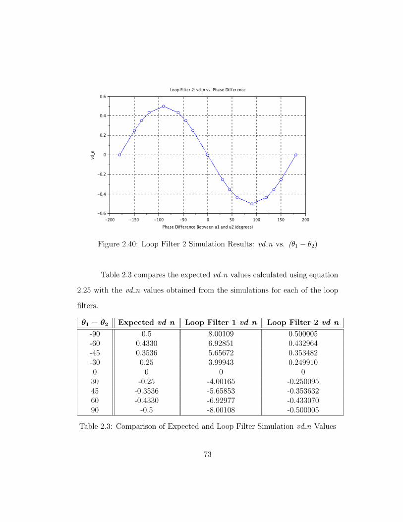
Figure 2.40: Loop Filter 2 Simulation Results: vd n vs. (θ1 − θ2)
Table 2.3 compares the expected vd n values calculated using equation
2.25 with the vd n values obtained from the simulations for each of the loop
filters.
θ1 − θ2 Expected vd n Loop Filter 1 vd n Loop Filter 2 vd n
-90 0.5 8.00109 0.500005-60 0.4330 6.92851 0.432964-45 0.3536 5.65672 0.353482-30 0.25 3.99943 0.2499100 0 0 030 -0.25 -4.00165 -0.25009545 -0.3536 -5.65853 -0.35363260 -0.4330 -6.92977 -0.43307090 -0.5 -8.00108 -0.500005
Table 2.3: Comparison of Expected and Loop Filter Simulation vd n Values
73

It is evident from Table 2.3 that the vd n values generated by “Loop
Filter 2” match the expected vd n values, while the vd n values generated by
“Loop Filter 1” would have to be scaled to match the expected values. This,
along with the facts presented below, lead to the selection of “Loop Filter 2”
for the ADPLL of this project.
• The design procedure of “Loop Filter 2” is better documented in [3] than
the design procedure for “Loop Filter 1” in [2].
• Resource calculations for implementing this project showed that a to-
tal of 14 multipliers would be required if “Loop Filter 2” was chosen
(12 multipliers would be needed if “Loop Filter 1” was chosen), while
the Xilinx Spartan-3AN FPGA has 20 available multipliers. Thus, the
project was not resource constrained with respect to multipliers.
2.2.2.2 NCO Architecture
Figure 2.41 shows the block diagram of the NCO designed for the AD-
PLL of this project. This NCO was designed to absorb the role of the Frequency
Divider block shown in the conceptual ADPLL block diagram of Figure 2.29.
Thus, the role of this NCO is twofold:
1. Generate the 19kHz sine wave (this is the u2 signal sent to the multi-
plier phase detector) that should be phase-locked to the recovered 19kHz
cosine pilot tone.
74

2. Generate the 38kHz cosine local oscillator signal that will be mixed with
the stereo component recovered by the 38kHz BPF of the demodulator.
This signal should also be phase-locked to the recovered pilot tone.
Figure 2.41: NCO Architecture for the Frequency Doubler BlockU(X,Y) are unsigned fixed-point signals with X integer and Y fractional bits
A(P,Q) are signed fixed-point signals with P integer and Q fractional bits
To accomplish the roles mentioned above, the following additional logic
was included: an extra LUT for generating the 38kHz cosine signal, and logic
that multiplied the output of the phase accumulator by two in order to pro-
vide the correct addressing for the 38kHz LUT. The multiply by two logic was
implemented as a left shift operation instead of an actual multiplication. In
memory constrained designs, additional mathematical logic can be designed
so that both of these LUTs can be combined into a single LUT that is appro-
75

priately addressed for generating both the 19kHz sine and the 38kHz cosine
signals. This is a possible future improvement to this NCO architecture.
The phase accumulator was designed to be a 24-bit accumulator, while
the LUTs were designed for a truncated 12-bit phase address word. The trun-
cated phase address word was chosen to be 12-bits since this would provide
a maximum possible phase truncation spur level of -72dBc as explained in
Section 2.2.1.3. Thus, with these architectural decisions, each of the LUTs
was designed to contain 4096 elements representing the amplitude values of
one complete cycle of a 1Hz sine wave and a 1Hz cosine wave sampled at
4.096kHz. Once again, additional mathematical logic can be designed to ex-
ploit the symmetry of the sine and cosine signals in order to reduce the size
of these LUTs. Many techniques have been developed in which the values for
a full cycle of a sine or cosine are obtained from mathematical manipulations
of the values of the first quarter of the phase cycle (i.e. the values from phase
angles 0 to π/2). The use of such techniques would reduce the size of the LUTs
to 1024 elements each. This is another possible future improvement to this
NCO architecture.
Using the architectural decisions made above, a reference clock fre-
quency fc of 192kHz (fc has the same value as Fs), and equation 2.22, the
76

frequency tuning word N was calculated as follows:
N =fout · 2M
fc(2.28)
=19kHz · 224
192kHz(2.29)
≈ 1, 660, 245 (2.30)
The Phase Tuning Word input of the NCO will be connected to the
Tuning Offset output from the amplifier A block shown on Figure 2.29. Thus,
it is the amplifier’s job to provide a Tuning Offset signal that will be appro-
priately processed by the NCO to effect the desired phase change in its output
signals. The section that follows describes how the amplifier A block was de-
signed so that it can provide the appropriate Phase Tuning Word input to the
NCO.
2.2.2.3 Amplifier A Architecture
As previously stated, the role of the amplifier A on Figure 2.29 is to
convert the vd n output from the loop filter to a Tuning Offset signal that can
be adequately processed by the NCO. The amplifier accomplishes this task
using the following three steps:
1. It first converts vd n into a phase difference value (θ1 − θ2), which will
henceforth be referred to as θdiff .
2. Next, it calculates a positive θoffset value based on the θdiff value and
the sign of vd n. The θoffset value needs to be positive because it will
77

be converted into the Tuning Offset value that the NCO will use. As
shown on Figure 2.41, all of the signals of the phase accumulator of the
NCO are in unsigned, fixed-point format. Therefore, the NCO expects
an unsigned (i.e. positive) value on its Phase Tuning Word input.
3. Finally, it converts the positive phase offset value θoffset into a Tuning
Offset value that is appropriate for the NCO architecture described in
Section 2.2.2.2.
The conversions listed above can be accomplished either in radians
or degrees. Degrees were chosen for this project since they are much easier
to interpret than radians. To perform the first conversion listed above, the
simulation results shown on Figure 2.40 were used because these results already
correlate vd n values with their corresponding θdiff values. Analysis of the
simulation results reveals that a linear approximation of vd n vs. θdiff can
be made for phase differences between -90°and +90° (of course, the linear
approximation is more accurate for the smaller range of -60° to +60°). This
linear approximation is shown with a red line on Figure 2.42.
From the linear approximation shown on Figure 2.42, an equation that
relates θdiff to vd n was derived using two data point pairs represented in
a (vd n , θdiff) format. Thus, using data points (0,0) and (-0.25,30), the
following equation was derived for θdiff in terms of vd n:
θdiff = −120 · vd n (2.31)
78

Figure 2.42: Linear Approximation of Loop Filter vd n vs. θdiff
It is evident from the linear approximation and from equation 2.31 that
positive vd n values yield negative θdiff values; while negative vd n values yield
positive θdiff values. As was previously stated, the Tuning Offset value needs
to be unsigned (i.e. positive); so the negative θdiff values need to be converted
to an equivalent positive value. This is easily accomplished by adding 360°
to the negative θdiff value, and assigning this value to θoffset. Equation 2.32
shows the value of θoffset based on the value of θdiff and the sign of vd n.
θoffset =
{θdiff if vd n < 0 (i.e. θdiff positive)
θdiff + 360° if vd n ≥ 0 (i.e. θdiff negative)(2.32)
The final step for obtaining the Tuning Offset value is to scale the
θoffset angle value appropriately based on the NCO architecture designed in
79

Section 2.2.2.2. The phase accumulator of the NCO was designed as a 24-bit
accumulator, which means that the phase angle range of 0° to 360° contains
224 points. In other words, the Digital Phase Wheel representing the NCO
designed in Section 2.2.2.2 contains 224 = 16, 777, 216 points. This means
that a phase accumulator counter increment of 1 represents an increment of
360224
degrees; or, conversely, that an increment of 1° is accomplished with an
increment of 46,603 of the phase accumulator counter value. Thus, the equa-
tion for converting the θoffset value to an equivalent Tuning Offset (i.e. phase
accumulator increment value) can be derived to be
Tuning Offset = 46, 603 · θoffset (2.33)
Equations 2.31, 2.32, and 2.33 are the equations used by the amplifier
A block to convert the loop filter’s vd n value to an appropriate Tuning Offset
value for the NCO. As will be seen in the following section, which specifies the
complete Frequency Doubler architecture, the circuits of the amplifier block
implement the equations derived in this section.
80

2.2.2.4 Complete Frequency Doubler ADPLL Architecture
As mentioned in Section 2.2.2.2, the NCO designed for the Frequency
Doubler ADPLL absorbed the role of the Frequency Divider block shown in the
conceptual ADPLL block diagram of Figure 2.29. Thus, Figure 2.43 shows the
updated conceptual block diagram for the Frequency Doubler ADPLL imple-
mented for this project. On the other hand, Figure 2.44 shows the complete
and detailed Frequency Doubler architecture that integrates the loop filter,
NCO, and amplifier designed in the previous sections. All of the additional
logic required for control, synchronization, and correct scaling of signals is also
included in the detailed architectural diagram.
Figure 2.43: Conceptual Frequency Doubler ADPLL Block Diagram for thisProject
81

Figure 2.44: Complete Frequency Doubler Architecture
The flowchart of Figure 2.45 shows the algorithm implemented in the
Frequency Doubler block for strobing and processing the vd n signal. The
strobe wait time of 500µs for the vd n signal was chosen for the following two
82

reasons:
1. Simulations showed that the vd n signal settled to its useful DC value
(a value that can be converted to a valid Tuning Offset value) in ap-
proximately 250µs. This is shown on Figure 2.46, which shows the vd n
transition times for an initial θdiff value of -90° followed by a change of
θdiff to 0°. Figure 2.46 shows that when θdiff is -90°, vd n reaches its
DC value of 0.5V in approximately 250µs; and that when θdiff changes
to 0° at a time of 1ms, vd n once again reaches its DC value of 0V in
approximately 250µs.
2. Since the 19kHz pilot tone does not contain any modulated data, no
sudden shifts in its frequency or phase are expected. This means that
once phase-lock is achieved to the 19kHz pilot tone, the vd n value should
remain near 0. Therefore, the vd n signal indicating the phase difference
between the 19kHz cosine pilot tone and the NCO’s 19kHz sine does not
have to be sampled at a very high rate.
83

Figure 2.45: Flow Chart for Strobing and Processing of vd n Values in theFrequency Doubler Block
84

Figure 2.46: vd n Transition Time for a θdiff Transition from -90° to 0°
Now that the architectures for the FIR filters and Frequency Doubler
have been designed, complete system-level simulations can be run to ensure
proper FM MPX signal modulation and demodulation. The Scilab models
used for this system-level simulation and the relevant simulation results will
be presented in the following section.
2.3 Complete Modulator and Demodulator System Sim-ulation
The overall Scilab model used for system-level simulations was already
presented on Figure 2.18. This model consists of the following main blocks:
• mpx modulator: this block generates the MPX Out signal defined by
85

equation 1.13. Figure 2.47 shows the internal connections for this block.
• 19kHz BPF: this block represents the 19kHz Band Pass Filter required
by the FM MPX Demodulator, and can be used to specify the discrete
transfer function of this specific filter.
• 38kHz BPF: this block represents the 38kHz Band Pass Filter required
by the FM MPX Demodulator, and can be used to specify the discrete
transfer function of this specific filter.
• 15kHz LPFs: these blocks represent both of the 15kHz Low Pass Filters
required by the FM MPX Demodulator. Just like the previous filter
blocks, these blocks can be used to specify the discrete transfer functions
of these specific filters.
• freq 2x: this block emulates the ADPLL that uses the recovered 19kHz
pilot tone to generate the 38kHz mixer signal for the recovered stereo
component of the MPX Out signal. Even though this block is not a
complete model for the Frequency Doubler ADPLL designed in Section
2.2.2.4, its output amplitude, phase, and frequency can be configured in
order to explore their effects on the demodulation process. Figure 2.48
shows the internal connections for this block.
Apart from the main blocks mentioned above, the model also includes
a mixer (multiplier), scaling blocks, and adders to complete all of the logic
required by the FM MPX Demodulator. Oscilloscopes are also included in
86
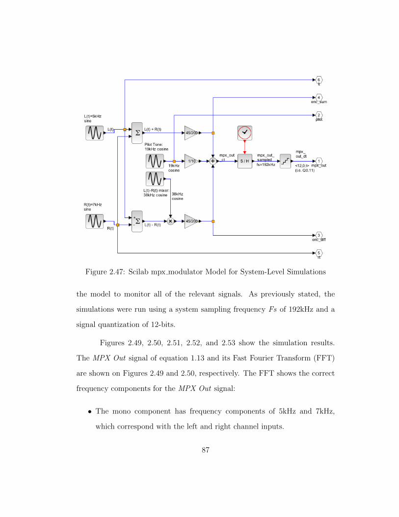
Figure 2.47: Scilab mpx modulator Model for System-Level Simulations
the model to monitor all of the relevant signals. As previously stated, the
simulations were run using a system sampling frequency Fs of 192kHz and a
signal quantization of 12-bits.
Figures 2.49, 2.50, 2.51, 2.52, and 2.53 show the simulation results.
The MPX Out signal of equation 1.13 and its Fast Fourier Transform (FFT)
are shown on Figures 2.49 and 2.50, respectively. The FFT shows the correct
frequency components for the MPX Out signal:
• The mono component has frequency components of 5kHz and 7kHz,
which correspond with the left and right channel inputs.
87
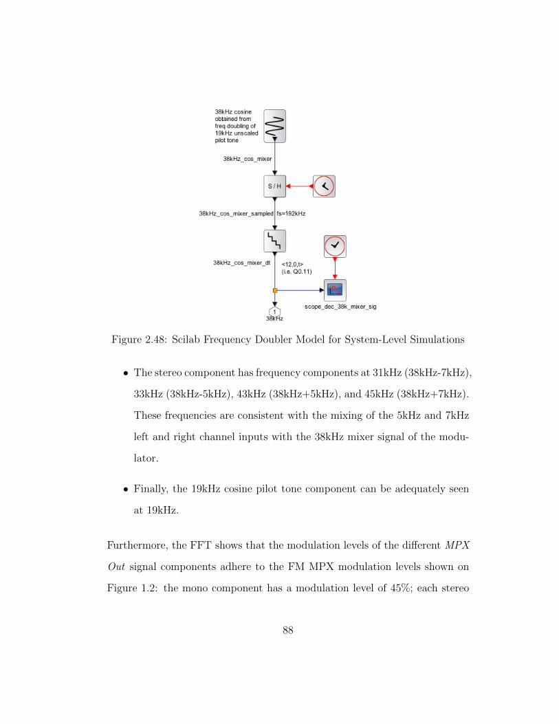
Figure 2.48: Scilab Frequency Doubler Model for System-Level Simulations
• The stereo component has frequency components at 31kHz (38kHz-7kHz),
33kHz (38kHz-5kHz), 43kHz (38kHz+5kHz), and 45kHz (38kHz+7kHz).
These frequencies are consistent with the mixing of the 5kHz and 7kHz
left and right channel inputs with the 38kHz mixer signal of the modu-
lator.
• Finally, the 19kHz cosine pilot tone component can be adequately seen
at 19kHz.
Furthermore, the FFT shows that the modulation levels of the different MPX
Out signal components adhere to the FM MPX modulation levels shown on
Figure 1.2: the mono component has a modulation level of 45%; each stereo
88

side-lobe component has a modulation level of 22.5%; and the pilot component
has a modulation level of 10%.
Figure 2.49: MPX Out Signal Generated by mpx modulator Scilab Model
Figure 2.50: FFT of MPX Out Signal Showing Frequency Components andModulation Levels
89

Finally, Figures 2.51, 2.52, and 2.53 show that the pilot, left channel,
and right channel signals are appropriately demodulated. Thus, the project
can proceed to the implementation of the designed system, which will be de-
scribed in Chapter 3.
Figure 2.51: Comparison of Modulated (top) and Demodulated (bottom)19kHz Pilot Tone
90

Figure 2.52: Comparison of Modulated (top) and Demodulated (bottom)Left Channel Signals
Figure 2.53: Comparison of Modulated (top) and Demodulated (bottom)Right Channel Signals
91

Chapter 3
Implementation on Xilinx Spartan-3AN
FPGA
Figure 3.1 shows the top-level module for the system implemented on
the Xilinx Spartan-3AN FPGA. Even though the system on the FPGA only
interfaces with the digital to analog converter (DAC) on the Starter Kit, the
top-level module includes signals for interfacing with the analog to digital
converter (ADC) as well. This was done so that, in the future, the MPX
Modulator LUT could be replaced with an actual MPX Modulator that accepts
left and right channel inputs from the ADC. The FPGA uses a Serial Peripheral
Interface (SPI) protocol to communicate with the DAC. Therefore, most of
the input and output signals of the FPGA top-level module are SPI signals,
which will be discussed in greater detail in Section 3.3.7. Thus, the module is
comprised of the following input ports:
• clk 133MHz: this is the input for an external clock that the FPGA uses
to generate all internal clocks. This clock is provided by a 133MHz clock
oscillator installed on the Xilinx Spartan-3AN Starter Kit.
• rst: this is the input for an external, active high reset signal. For this
project, this input is connected to the BTN NORTH push button of the
92

Starter Kit.
• adc out: this is the SPI input for serial data from the analog to digital
converter (ADC) present on the Starter Kit. This input is unused for
this project.
Furthermore, the top-level module has the following output ports:
• ad conv: this signal is not used in this project because it is intended to
provide a “begin conversion” strobe pulse to the ADC.
• amp cs: this signal is an active low signal that selects the ADC as the
desired slave device for the SPI communication. This signal is not used
in this project.
• dac clr: this signal is an active low signal used for resetting the DAC.
• dac cs: this signal is an active low signal that selects the DAC as the
desired slave device for the SPI communication.
• spi mosi: this is the SPI data signal that sends the serial data from the
SPI master device (i.e. the FPGA) to the slave devices (i.e. either the
ADC or the DAC).
• spi sck: this is the SPI clock signal that synchronizes the SPI communi-
cation between the FPGA and the slave devices.
93

Figure 3.1: Top Level Module Implemented on the Xilinx Spartan-3ANFPGA
The remainder of this chapter will be dedicated to the details of the
design implemented on the FPGA. First, the clock and reset schemes will be
presented; followed by detailed descriptions of each of the sub-modules that
were integrated to create the top-level module of Figure 3.1. The chapter will
conclude with a brief summary of the resulting FPGA resource utilization for
this project.
94

3.1 Clock Scheme
Four different clock domains are present in the design implemented on
the FPGA: 133MHz, 13.3MHz, 98.304MHz, and 192kHz. The 133MHz clock
is provided by the external clock oscillator and is used to generate all of the
other clock domains. The 13.3MHz clock domain is obtained from dividing the
133MHz input clock by 10, and is only used for the debounce logic for the reset
signal. Since the reset signal is being provided by a push button, debounce
logic is required to prevent undesired “bouncing” or ringing of this signal. This
debounce logic was mirrored after a Xilinx example that used a 13.3MHz clock,
but similar results could most likely be achieved using either the 98.304MHz
or 192kHz clock domains. Thus, the elimination of the 13.3MHz clock domain
is a possible future improvement to the clock scheme of this design.
Unlike the 13.3MHz clock domain, which is only used by the debounce
logic, the 192kHz and 98.304MHz clock domains are used by the majority
of the circuits of this design. As previously mentioned, the system sampling
frequency Fs chosen for this project is 192kHz. In order to generate the 192kHz
Fs clock, the 133MHz input clock had to first be divided down to a 512Fs
clock (i.e. 98.304MHz), which subsequently was divided by 512 to generate
the 192kHz clock. The 512Fs clock is used to clock all of the FIR filters, the
spi controller mpx enc sub-module, and the spi top sub-module. It is also used
to generate many of the synchronization signals used in the design. On the
other hand, the Fs clock is used by the mpx encoder module to generate the
MPX Out signal. It is also used to clock all of the circuitry in the mpx decoder
95

sub-module except for the FIR filters. Last but not least, the Fs clock is used
to pipeline and synchronize all of the signals in the mpx decoder sub-module.
3.2 Reset Scheme
Internally, the FPGA uses two active-high reset signals called rst debounced
and rst global to hold all of the sub-modules in reset. The rst debounced sig-
nal is used to keep the dcm1 sub-module in reset and is connected to the
top-level rst input signal through the debounce logic. On the other hand, the
rst global signal is used to keep all other sub-modules in reset, and is also
inverted in order to provide the active-low, top-level dac clr output signal for
resetting the DAC. This rst global signal is generated from the logical OR of
the rst debounced signal and the inverted LOCKED OUT output from the
dcm1 sub-module. Hence, it is activated when one or both of the following
conditions occur:
1. The BTN NORTH push button on the Starter Kit is pressed.
2. The LOCKED OUT output signal of the dcm1 sub-module is low, in-
dicating that the 512Fs clock is not present. Since the 512Fs clock is
used to generate the Fs clock, and since both of these clocks are used by
the majority of the logic, it makes sense to keep all sub-modules in reset
when these clocks are absent.
The purpose of the reset scheme described above is to initialize all logic
appropriately so that all sub-modules of the top-level FPGA system function
96

properly once the reset signal is de-asserted.
3.3 Module Descriptions
Figure 3.2 shows all of the sub-modules that were integrated to form
the complete top-level module of the FPGA. In the next few sections, each
of these sub-modules will be described in detail with the following modular
format: first the sub-module’s purpose will be described, followed by the block
diagram; and, finally, any additional details regarding the design of the sub-
module, such as internal block diagrams or Finite State Machines (FSMs), will
be presented.
97

Figure 3.2: Sub-Modules of the Top-Level FPGA Design
98

3.3.1 Sub-Module: clk div 10
Below are the details for the clk div 10 sub-module.
• Purpose: divide the 133MHz input clock by 10 to generate a 13.3MHz
clock for the debounce sub-module.
• Top-Level Diagram:
Figure 3.3: Top-Level Diagram of clk div 10 Sub-Module
• Additional Details: this sub-module was taken from a Xilinx example.
Furthermore, this sub-module uses a 4-bit counter to divide the 133MHz
clock down to 13.3MHz, while still retaining a 50% duty cycle. This
division is accomplished by outputting either a zero or a one based on
the counter value, which is incremented on every rising clock edge of the
input clock. In this particular case, the following output values were
generated for the following counter values:
99

– (0 ≤ counter < 5): output a 0
– (5 ≤ counter < 10): output a 1
– (10 ≥ counter): reset counter to 1 and output a 0
3.3.2 Sub-Module: debounce
Below are the details for the debounce sub-module.
• Purpose: correctly decode the reset pulse generated when the BTN NORTH
push button is pressed.
• Top-Level Diagram:
Figure 3.4: Top-Level Diagram of debounce Sub-Module
• Additional Details: this sub-module was taken from a Xilinx example.
Mechanical switches used for generating an electrical pulse, such as push
100

buttons, can “bounce” and cause the electrical signal that they are gen-
erating to ring. This can lead to multiple pulses being erroneously de-
tected. The ringing of the electrical signal can be controlled by a “de-
bounce” circuit that strobes the previous values of the signal and com-
pares them to the current value in order to eliminate the detection of
multiple erroneous pulses.
3.3.3 Sub-Module: dcm1
Below are the details for the dcm1 sub-module.
• Purpose: generate the 512Fs (i.e. 98.304MHz) clock from the 133MHz
input clock.
• Top-Level Diagram:
Figure 3.5: Top-Level Diagram of dcm1 Sub-Module
101

• Additional Details: this sub-module is a Digital Clock Manager (DCM)
module that is available on Xilinx Spartan-3AN FPGAs. The specific
FPGA used on the Starter Kit has eight available DCMs. DCMs inte-
grate advanced clocking capabilities into the FPGA’s global clock distri-
bution network. One of these capabilities is the multiplication or divi-
sion of an incoming clock frequency in order to synthesize a completely
new frequency. This capability is achieved through the mixture of clock
multiplication and division values, which are specified during the DCM
instantiation process [21]. To generate the 512Fs clock from the 133MHz
clock, 17 and 23 were specified as the clock multiplication and division
values, respectively, since the multiplication of 133MHz with 1723
is equal
to 98.304MHz.
3.3.4 Sub-Module: clk div 512
Below are the details for the clk div 512 sub-module.
• Purpose: divide the 512Fs clock by 512 to generate the 192kHz Fs clock.
• Top-Level Diagram:
102

Figure 3.6: Top-Level Diagram of clk div 512 Sub-Module
• Additional Details: this sub-module uses a 9-bit counter to divide the
98.304MHz clock down to 192kHz, while still retaining a 50% duty cycle.
This division is accomplished by outputting either a zero or a one based
on the counter value, which is incremented on every rising clock edge of
the input clock. In this particular case, the following output values were
generated for the following counter values:
– (0 ≤ counter < 256): output a 0
– (256 ≤ counter < 512): output a 1
3.3.5 Sub-Module: mpx encoder
Below are the details for the mpx encoder sub-module.
103

• Purpose: generate the MPX Out signal specified by equation 1.13 sam-
pled at Fs.
• Top-Level Diagram:
Figure 3.7: Top-Level Diagram of mpx encoder Sub-Module
• Additional Details: as shown on Figure 3.8, this sub-module uses a
counter and a look-up-table (LUT) to generate the MPX Out signal
that will be sent to the mpx decoder sub-module for demodulation. The
LUT contains 192 elements that represent the values of the MPX Out
signal sampled at 192kHz (the elements are in 12-bit, signed, fixed-point
format). These LUT elements are addressed by the 8-bit output of the
counter, which is incremented on each rising edge of the Fs clock and is
reset back to 0 after the counter value reaches 191.
104

Figure 3.8: Internal Block Diagram of mpx encoder Sub-Module
3.3.6 Sub-Module: mpx decoder
Below are the details for the mpx decoder sub-module.
• Purpose: demodulate the 19kHz pilot tone, left channel, and right chan-
nel signals from the MPX Out signal generated by the mpx encoder sub-
module.
• Top-Level Diagram:
105

Figure 3.9: Top-Level Diagram of mpx decoder Sub-Module
• Additional Details: this sub-module integrates all of the FIR filters and
the Frequency Doubler block designed in Chapter 2 to implement the FM
MPX Demodulator. This sub-module also includes all of the necessary
synchronization and scaling required to properly demodulate the 19kHz
pilot tone, left channel, and right channel signals. In order to properly
synchronize all signals, the signal data flow for this module was divided
into five pipeline stages. Figure 3.10 shows a detailed block diagram of
the final circuit implemented in this sub-module; while Figure 3.11 shows
the operations performed during each stage of the five-stage pipeline.
The numbers in parenthesis next to each block on Figure 3.10 indicate
the associated pipeline stage for that block.
106

Figure 3.10: Internal Block Diagram of Final Circuit for mpx decoderSub-Module
107

Figure 3.11: Pipeline Schedule for mpx decoder Sub-Module
The main functional blocks of the mpx decoder sub-module are the FIR
filters and the Frequency Doubler block. The detailed block diagram
for the Frequency Doubler block was already shown on Figure 2.44. As
for the FIR filters, they were implemented using Xilinx’s FIR Compiler
Tool. Even though Figure 2.1 is useful for undertanding the computa-
tion performed by a FIR filter, the actual implementation of the filter
on the FPGA is quite different. The FIR filters for this project were im-
plemented using a single multiply-accumulate (MAC) engine along with
separate memories for storing input data values and coefficient values,
as shown on Figure 3.12 [19]. The MAC engine has the following func-
tionality: on each cycle of the clock used for the FIR filter, the partial
product of a filter coefficient with its corresponding input data is calcu-
108

lated, and the result is accumulated with the accumulator logic formed
by the delay element (e.g. register) and adder. For this design, the FIR
filters had to generate one output sample on every rising edge of the
Fs clock. Thus, only one MAC engine was required to implement each
FIR filter since each filter has less than 512 coefficients and is clocked by
the 512Fs clock. If more than 512 coefficients were required by the FIR
filters, then they would have had to be implemented with multiple MAC
engines in order to meet the desired throughput of one output sample
every Fs clock edge.
Figure 3.12: FIR Implementation on FPGA
Using Xilinx’s FIR Compiler Tool, many of the other FIR filter specifica-
tions, such as input data width and format, could be configured. Thus,
109
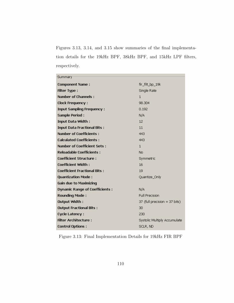
Figures 3.13, 3.14, and 3.15 show summaries of the final implementa-
tion details for the 19kHz BPF, 38kHz BPF, and 15kHz LPF filters,
respectively.
Figure 3.13: Final Implementation Details for 19kHz FIR BPF
110

Figure 3.14: Final Implementation Details for 38kHz FIR BPF
111

Figure 3.15: Final Implementation Details for 15kHz FIR LPF
3.3.7 Sub-Module: spi top
Below are the details for the spi top sub-module.
• Purpose: sends the demodulated pilot, left channel, and right channel
112

data to DAC Channels A, B, and C, respectively, using the Serial Pe-
ripheral Interface (SPI) protocol.
• Top-Level Diagram:
Figure 3.16: Top-Level Diagram of spi top Sub-Module
• Additional Details: this sub-module is a SPI Core for use with Xilinx
Starter Kits written by William Gibb and downloaded from OpenCores
(http://opencores.org/), which is a site that hosts open source hardware
113

IP cores. Before proceeding to the specifics of the SPI communication
with the DAC on the Starter Kit, a brief introduction to the SPI bus will
be provided. The SPI bus was developed by Motorola to provide full-
duplex synchronous serial communication between a master device (e.g.
a microcontroller or an FPGA) and multiple slave devices (e.g. DACs
or ADCs) [4]. As shown on Figure 3.17, SPI masters communicate with
slave devices using serial clock (SCK), Master Out Slave In (MOSI),
Master In Slave Out (MISO), and Slave Select (SS) signals [4]. The
SCK, MOSI, and MISO signals can be shared by slaves, but each slave
requires a dedicated SS signal.
Figure 3.17: SPI Configuration of one Master with Multiple Slaves
Figure 3.18 shows the particular SPI connections between the Xilinx
FPGA and the DAC used on the Starter Kit, while Figure 3.19 shows
114

the SPI waveforms required for sending data to the DAC [20]. It is evi-
dent from Figure 3.18 that the four general SPI connections are present,
along with an additional, DAC CLR signal. This additional signal is
an asynchronous, active-low reset signal for the DAC. The SPI commu-
nication waveforms of Figure 3.19 show that the FPGA should do the
following to transfer data to the DAC [7]:
1. Drive the DAC CS signal low to select the DAC as the slave device.
2. Transmit data on the SPI MOSI signal (MSB first) such that the
DAC can capture the data on the rising edge of the SPI SCK clock.
3. Complete the SPI bus transaction by returning the DAC CS signal
high.
Figure 3.18: SPI Connections Between FPGA and DAC
115

Figure 3.19: SPI Data Transfer Waveforms for FPGA Write to DAC
The DAC uses a 24-bit protocol that includes 4 command bits, 4 address
bits, 12 data bits, and 4 don’t care bits as shown on Figure 3.20 [20].
Figure 3.21 shows how the DAC interprets the command and address
nibbles sent to it by the FPGA [15].
Figure 3.20: DAC 24-bit Protocol
116

Figure 3.21: DAC Command and Address Nibbles Decoding
Thus, the spi top sub-module implements the SPI communication wave-
forms shown on Figure 3.19 in order to transfer data from the FPGA
to the DAC. It accomplishes this through the use of internal CTRL and
Data TX registers that can be configured using control words and con-
trol signals. The following process is used to write data to the DAC
Channels [7]:
1. Set the TXC bit in the CTRL register to enable the writing of data
into the Data TX register. The setting of this bit is accomplished by
sending the CTRL TXC control word (whose hexadecimal value is
0x002E18) into the data in(23:0) input while asserting the load ctrl
input.
117

2. Write the Data TX register with the 24-bit data that needs to be
sent to the DAC. This is accomplished by sending the 24-bit data
word into the data in(23:0) input.
3. Set the GO and WRITE bits in the CTRL register to begin the SPI
transmission. The setting of these bits is accomplished by sending
the CTRL GOWRITE control word (whose hexadecimal value is
0x000F98) into the data in(23:0) input while asserting the load ctrl
input. No additional writes to the CTRL register can be performed
while transmission is in progress, which is indicated by the go out-
put signal being high. Once go is de-asserted, the process can be
re-started at Step 1.
All of the register writes mentioned above are accomplished by the
spi controller mpx enc sub-module, which will be described in the fol-
lowing section.
3.3.8 Sub-Module: spi controller mpx enc
Below are the details for the spi controller mpx enc sub-module.
• Purpose: control the spi top sub-module so that it transfers the demod-
ulated data from the mpx decoder to the appropriate DAC Channels.
• Top-Level Diagram:
118

Figure 3.22: Top-Level Diagram of spi controller mpx enc Sub-Module
• Additional Details: this sub-module formats the demodulated signals
from the mpx decoder and sends this data along with the appropriate
command sequence to the spi top sub-module. To achieve this role, this
sub-module does the following:
– Concatenates appropriate DAC address and command nibbles (shown
on Figures 3.20 and 3.21) to the 12-bit pilot tone, left channel,
and right channel data words it receives from the mpx decoder sub-
119

module. This is done to form the 24-bit data word that will be
loaded into the spi top’s Data TX register.
– Implements the Finite State Machine (FSM) shown on Figure 3.23.
This FSM writes the CTRL and Data TX registers of the spi top
sub-module with the appropriate values to send the pilot tone, left
channel, and right channel data to DAC Channels A, B, and C,
respectively.
As mentioned in Section 3.3.7, the CTRL TXC and CTRL GOWRITE
data words that appear on Figure 3.23 are control data words that can
be used to set bits of the spi top’s CTRL register. Furthermore, hand-
shaking between these two sub-modules is accomplished through the tip
input of the spi controller mpx enc sub-module, which is connected to
the go output of the spi top sub-module.
The FSM shown on Figure 3.23 has 15 active states, which are described
below.
– State Init: initial and reset state of the FSM. Any reset pulse will
cause a return to this state.
– State Set Div: state to set the value of the divider used to generate
the SPI serial clock on the sclk pad o output pin of the spi top sub-
module. After writing the divider value, the FSM will remain in
this state until it receives the initial demodulated data from the
120

mpx decoder, which is indicated by the assertion of the internal
dac chan change signal.
– State TXC ChanA: state to set the TXC bit of the CTRL register
to capture the 24-bit data to be written to DAC Channel A.
– State Data ChanA: state that loads the 24-bit data into the Data
TX register. This data includes the 12-bit demodulated pilot tone
data from the mpx decoder sub-module.
– State Write ChanA: state that sets the WRITE and GO bits of the
CTRL register to start the write to DAC Channel A.
– State TIP ChanA: transfer in progress state for DAC Channel A.
The FSM will remain in this state as long as the go signal from the
spi top sub-module is set. This is to allow for completion of the
data transfer to DAC Channel A.
– State TXC ChanB: state to set the TXC bit of the CTRL register
to capture the 24-bit data to be written to DAC Channel B.
– State Data ChanB: state that loads the 24-bit data into the Data
TX register. This data includes the 12-bit demodulated left channel
data from the mpx decoder sub-module.
– State Write ChanB: state that sets the WRITE and GO bits of the
CTRL register to start the write to DAC Channel B.
– State TIP ChanB: transfer in progress state for DAC Channel B.
The FSM will remain in this state as long as the go signal from the
121

spi top sub-module is set. This is to allow for completion of the
data transfer to DAC Channel B.
– State TXC ChanC: state to set the TXC bit of the CTRL register
to capture the 24-bit data to be written to DAC Channel C.
– State Data ChanC: state that loads the 24-bit data into the Data
TX register. This data includes the 12-bit demodulated right chan-
nel data from the mpx decoder sub-module.
– State Write ChanC: state that sets the WRITE and GO bits of the
CTRL register to start the write to DAC Channel C.
– State TIP ChanC: transfer in progress state for DAC Channel C.
The FSM will remain in this state as long as the go signal from the
spi top sub-module is set. This is to allow for completion of the
data transfer to DAC Channel C.
– State TX Write Complete: state to indicate completion of writes
to DAC Channels A, B, and C. The FSM will remain in this state
until the new pilot tone, left channel, and right channel data values
are received from the mpx decoder sub-module, which is indicated
by the assertion of the internal dac chan change signal.
122

Figure 3.23: FSM Implemented by the spi controller mpx enc Sub-Module
123

3.4 FPGA Resource Utilization
Figure 3.24 shows the FPGA resource utilization for the final imple-
mented design. As can be seen from this resource utilization summary, the
design was easily implementable on the Starter Kit’s FPGA.
Figure 3.24: FPGA Resource Utilization for Final Implemented Design
124

Chapter 4
System Validation
The validation approach mirrored the implementation approach: both
were performed incrementally. Thus, an iterative process of implementing
certain sub-modules of the entire system and validating the functionality of
just those sub-modules led to the final implementation and validation of the
complete system. The process for arriving at a complete system was broken
into the following three stages:
1. Stage 1: implementation and validation of the SPI, MPX Encoder, and
19kHz Band Pass Filter (BPF) sub-modules.
2. Stage 2: implementation and validation of the Frequency Doubler AD-
PLL sub-module.
3. Stage 3: implementation and validation of the complete system shown
on Figure 3.2.
Each of the stages listed above will be discussed in greater detail in the
sections that follow. But, before doing so, a brief explanation of the terms
“implementation” and “validation” for this project are in order. The “imple-
mentation” of a sub-module involved writing the register transfer level (RTL)
125

source code for the sub-module (this was done using Verilog); performing be-
havioral simulations on the RTL model; synthesizing the RTL model into a
programmable “bit file” (i.e. netlist); and finally programming the “bit file”
onto the FPGA. On the other hand, the “validation” of a sub-module (or a
group of sub-modules) consisted of capturing waveforms from DAC Channels
A, B, and C with an oscilloscope; and then comparing the captured wave-
forms with expected waveforms generated during the simulations described in
Chapter 2.
4.1 Validation of SPI, MPX Encoder, and 19kHz BPF
Following is a list of the first set of sub-modules that were imple-
mented to create the first validation sub-system: clk div 10, debounce, dcm1,
clk div 512, mpx encoder, fir filt bp 19k, spi controller mpx enc, and spi top.
In addition to the sub-modules already listed, this sub-system contained a
debug sub-module used for generating a 19kHz cosine pilot tone with iden-
tical phase as the pilot tone contained in the MPX Out signal. This debug
sub-module consisted of a counter and look-up-table (LUT) for generating the
19kHz cosine pilot tone. Its output was used to ensure that the pilot tone
recovered by the 19kHz BPF had the same frequency and phase as the pilot
tone in the MPX Out signal.
This first sub-system was implemented to validate the functionality
of the mpx encoder, fir filt bp 19k, spi controller mpx enc, and spi top sub-
modules. Thus, the validation of this sub-system ensured the following:
126
1. That the SPI sub-modules properly routed data from within the FPGA
to DAC Channels A, B, and C.
2. That the MPX Out signal was being properly generated by the mpx encoder
sub-module.
3. That the 19kHz pilot tone was properly recovered by the fir filt bp 19k
sub-module from the MPX Out signal.
Figures 4.1, 4.3, and 4.4 show the oscilloscope screen shots for the
validation performed on this sub-system. Below is a description of the signals
captured with the oscilloscope.
• Green Waveform: 19kHz cosine pilot tone generated by the debug sub-
module and output to DAC Channel C.
• Blue Waveform: 19kHz cosine pilot tone recovered by the fir filt bp 19k
sub-module and output to DAC Channel B.
• Yellow Waveform: MPX Out signal generated by the mpx encoder sub-
module and output to DAC Channel A.
The fact that the waveforms listed above were captured with an oscilloscope
confirms that the SPI sub-modules were properly sending internal FPGA sig-
nals to the different DAC Channels. Thus, this validates the functionality of
the spi controller mpx enc and spi top sub-modules.
127

Figure 4.1: Yellow Waveform: MPX Out Signal Generated by mpx encoderSub-Module
Figure 4.2: MPX Out Signal from Scilab Simulations
128

Figure 4.3: Frequency Comparison of Generated 19kHz Pilot Tone (GreenWaveform) with Recovered 19kHz Pilot Tone (Blue Waveform)
A comparison of Figures 4.1 and 4.2 shows the following: the oscil-
loscope captured MPX Out signal matches the MPX Out signal waveform
obtained during system-level simulations with Scilab. Thus, the mpx encoder
sub-module is properly generating the MPX Out signal.
Figures 4.3 and 4.4 validate that the 19kHz cosine pilot tone is being
properly recovered by the fir filt bp 19k sub-module. In particular, Figure 4.3
shows that the pilot tone generated by the debug sub-module and the recovered
pilot tone are both at 19.08kHz; while Figure 4.4 shows that the generated and
recovered pilot tones have a phase difference of 1.6µs, which coincides with the
phase difference seen during system-level simulations (see Section 2.1.3.5 and
Figure 2.26). This completes the validation of the first sub-system.
129

Figure 4.4: Measured Phase Difference Between Generated 19kHz Pilot Tone(Green Waveform) and Recovered 19kHz Pilot Tone (Blue Waveform)
4.2 Validation of Frequency Doubler
Building upon the sub-system validated in the first stage, the second
stage of implementation and validation incorporated the freq doubler sub-
module (this sub-module is one of the main components of the mpx decoder
sub-module) into the sub-system. Thus, the objective of the second stage of
validation was to ensure that the freq doubler sub-module properly frequency
doubled the recovered 19kHz pilot tone to generate a 38kHz cosine signal. In
addition to being at twice the frequency of the recovered pilot tone, the gen-
erated 38kHz cosine signal is required to be phase-locked to the pilot tone.
Once again, the debug sub-module was used to generate a 19kHz pilot tone
with exactly the same phase as the pilot tone in the MPX Out signal. This
generated 19kHz pilot tone is used to ensure that both the recovered pilot tone
130

and the 38kHz frequency-doubled cosine signal have the correct phase.
Figures 4.5 and 4.6 show the oscilloscope screen shots for the valida-
tion performed on this sub-system that includes the freq doubler sub-module.
Below is a description of the signals captured with the oscilloscope.
• Green Waveform: 19kHz cosine pilot tone generated by the debug sub-
module and output to DAC Channel C.
• Blue Waveform: full scale 19kHz cosine pilot tone obtained by multiply-
ing the recovered pilot tone by 10. As before, the pilot tone is recovered
by the fir filt bp 19k sub-module; while the multiplication by 10 is per-
formed in the freq doubler sub-module. This full scale pilot tone is output
to DAC Channel B.
• Yellow Waveform: 38kHz frequency doubled output from the freq doubler
sub-module. This 38kHz frequency doubled signal is output to DAC
Channel A.
131

Figure 4.5: Frequency and Phase Comparison of Generated 19kHz Pilot Tone(Green Waveform), Full Scale 19kHz Pilot Tone (Blue Waveform), and
Frequency Doubled 38kHz Signal (Yellow Waveform)
Figure 4.6: Zoomed View: Frequency and Phase Comparison of Generated19kHz Pilot Tone (Green Waveform), Full Scale 19kHz Pilot Tone (Blue
Waveform), and Frequency Doubled 38kHz Signal (Yellow Waveform)
132

The oscilloscope screen shots on Figures 4.5 and 4.6 show that the
recovered full scale pilot tone and the 38kHz frequency doubled signal have
the same phase. In addition, the screen shots show that the aforementioned
signals have the same phase as the 19kHz pilot tone generated by the debug
sub-module. Last but not least, the screen shots show that the frequency
of the full scale pilot tone is nominally 19kHz, while the frequency of the
frequency doubled signal is nominally 38kHz. This concludes the validation
of the freq doubler sub-module. The project can now proceed to the complete
system implementation and validation stage.
4.3 Validation of Complete System
Once again, building on the sub-system validated in the second stage,
the third and final stage of implementation and validation incorporated the
mpx decoder sub-module into the sub-system. This resulted in the complete
system shown on Figure 3.2. The initial design of the mpx decoder sub-module
used the FIR filters summarized on Table 2.2. Thus, the initial mpx decoder
sub-module used to obtain the complete system had a 19kHz BPF of order
N =442, and 38kHz BPF and 15kHz LPFs of order N =384. Furthermore, this
initial mpx decoder design did not include the sync sum x 0p5 block shown on
Figure 3.10. This sync sum x 0p5 block was added as a result of the validation
described in this section. It should also be noted that the debug sub-module
used to generate the 19kHz reference pilot tone in the previous validation
stages was removed from the complete system implementation.
133

The initial validation of the complete system showed that the 19kHz
pilot tone was being properly recovered, but that the left and right channel
signals were not being properly demodulated. Even though no oscilloscope
screen shots were taken, the probed left and right channel signals resembled
the demodulated left and right channel signals seen on Figures 2.19 and 2.20
obtained during the Scilab simulations of the FIR filters. In order to debug
the complete system, a “simulation analysis” RTL version of the complete
system was designed. This “simulation analysis” version brought all of the
internal mpx decoder signals to the top-level system module shown on Figure
3.1. By making all of the internal mpx decoder signals additional outputs of
the top-level system module, their RTL behavioral simulation values could be
captured in a text file. In turn, the text file could be post-processed using
a Perl script and Scilab in order to view plots of the different signals being
generated within the mpx decoder sub-module.
Analysis of the RTL behavioral simulation values revealed that all in-
dividual signals within the mpx decoder sub-module were being properly gen-
erated, but that they did not have the correct phase relative to each other.
In other words, for proper demodulation to occur, all of the signals gener-
ated by the different blocks within the mpx decoder sub-module would have
to be properly synchronized to each other. The first step taken to accomplish
this synchronization was to convert the 38kHz BPF and 15kHz LPFs to order
N =442. This was done so that all FIR filters within the mpx decoder sub-
module would have the same order, and would thereby generate their output
134

values after receiving the same number of input samples. Behavioral simula-
tion results with these new filters revealed that the signals generated by the
fir filt bp 19k, fir filt bp 38k, and fir filt lp 15k sum blocks of Figure 3.10 were
properly synchronized to each other, but that the left and right channel signals
were still not being properly demodulated.
Further analysis of the behavioral simulation results revealed that the
sum x 0p5 and diff x 0p5 signals shown on Figure 3.10 were not properly syn-
chronized with each other. Since these are the last set of signals that are added
and subtracted from each other to recover the left and right channel signals,
they need to be properly synchronized to each other for the desired demod-
ulation to occur. Figure 4.7 shows how these signals should be synchronized
with each other for proper demodulation to occur; while Figure 4.8 shows the
relative phase that these signals had to each other based on the behavioral
simulations.
135

Figure 4.7: Required Synchronization of sum x 0p5 and diff x 0p5 Signalsfor Proper Left and Right Channel Demodulation
136

Figure 4.8: Relative Phase of sum x 0p5 and diff x 0p5 Signals fromBehavioral Simulations with All FIR Filters of Order N =442
137

The labeled data points of Figure 4.7 show two points that need to
be synchronized with each other on the sum x 0p5 and diff x 0p5 signals for
proper demodulation to occur. The labeled data points of Figure 4.8 show that
the two points that should be synchronized for proper demodulation to occur
are actually occurring 29 Fs clock cycles from each other. In particular, Figure
4.8 shows that the diff x 0p5 signal is delayed by 29 Fs clock cycles relative
to the sum x 0p5 signal. Thus, in order for proper left and right channel
demodulation to occur, the sum x 0p5 signal needs to be delayed by 29 Fs
clock cycles so that it is adequately synchronized with the diff x 0p5 signal.
This delay was accomplished through the introduction of the sync sum x 0p5
block into the mpx decoder sub-module.
Behavioral simulations with the debugged mpx decoder (i.e. the mpx decoder
with FIR filters of order N =442 and with the new sync sum x 0p5 block) re-
vealed proper demodulation of the left and right channel signals. Thus, the
“simulation analysis” RTL version of the complete system was changed into
an “implementable” version which removed all of the internal mpx decoder
signals from the top-level system module. This “implementable” version of
the complete system is the one shown on Figure 3.1. Validation of the com-
plete system resulted in the oscilloscope screen shots shown on Figures 4.9 and
4.10, which show that the pilot tone, left channel, and right channel signals
are properly demodulated. Below is a description of the signals captured with
the oscilloscope.
• Yellow Waveform: full scale recovered 19kHz cosine pilot tone output to
138

DAC Channel A.
• Blue Waveform: demodulated left channel 5kHz sine wave output to
DAC Channel B.
• Green Waveform: demodulated right channel 7kHz sine wave output to
DAC Channel C.
Figure 4.9: Oscilloscope Screen Shot of Full-Scale Recovered 19kHz PilotTone (Yellow Waveform), Demodulated 5kHz Left Channel (Blue
Waveform), and Demodulated 7kHz Right Channel (Green Waveform)
The debugging performed above describes what was done in order to
achieve proper demodulation of the left and right channel signals, yet the
question remains as to why the sum x 0p5 signal needed to be delayed by 29
Fs clock cycles for it to be properly synchronized with the diff x 0p5 signal.
Analysis of the mpx decoder block diagram of Figure 3.10 reveals that the
139

Figure 4.10: Zoomed View of Oscilloscope Screen Shot of Full-ScaleRecovered 19kHz Pilot Tone (Yellow Waveform), Demodulated 5kHz LeftChannel (Blue Waveform), and Demodulated 7kHz Right Channel (Green
Waveform)
signal path that leads to the diff x 0p5 signal goes through an extra FIR filter
as compared with the signal path that leads to the sum x 0p5 signal. As shown
on Figure 3.10, there is only one FIR filter (the fir filt lp 15k sum filter) in the
signal path leading to the sum x 0p5 signal; while there are two FIR filters
(the fir filt bp 38k and fir filt lp 15k diff filters) in the signal path leading to
the diff x 0p5 signal. Thus, the output time delay of this extra filter in the
diff x 0p5 signal path, which is 29 Fs clock cycles, needs to be accounted
for in order to achieve the correct synchronization between the sum x 0p5
and diff x 0p5 signals. This concludes the implementation, validation, and
debugging of the complete system.
140

Chapter 5
Conclusion
Figure 4.9 shows that the overall goal of the project was achieved: a
fully digital system was developed to demodulate the pilot tone, left channel,
and right channel signals from a digital baseband FM MPX modulated signal.
In order to achieve this goal, all of the different levels of abstraction applied
to integrated circuit (IC) design were used.
The design started with an initial specification, which progressed to a
series of conceptual block diagrams describing the different functional blocks
required to implement the entire system. Figures 1.1, 1.3, and 1.4 are exam-
ples of such conceptual block diagrams. Then, each of the block diagrams was
sub-divided into sub-modules which could be explored and refined using high-
level simulation programs, such as Scilab. The high-level simulations helped in
understanding the functionality for the different sub-modules and the effects
of different architectures on the sub-module behavior and implementation. In
this particular project, the high-level simulations were used to understand
the functionality of the phase detector and loop filter in ADPLL (all digi-
tal phase-locked loop) applications. Furthermore, the high-level simulations
helped in defining the detailed Frequency Doubler and FIR filter architectures
141

that would be used to implement the system. Last but not least, the high-level
simulations provided invaluable plots of all of the signals involved in the mod-
ulation and demodulation of the FM MPX signal chosen for this project. It is
because of these signal plots that the final validation and debug were possible.
Development of structural or behavioral register transfer level (RTL)
models of the different sub-blocks followed the high-level simulations. Once
again, developing the RTL models required refining the sub-blocks with actual
input and output port specifications, data flow and control logic specifications,
bit manipulations, and behavioral specifications through finite state machines
(FSMs). For example, in order to convert the Frequency Doubler Architecture
shown on Figure 2.44 into a structural RTL model, the fixed-point representa-
tion for every signal had to be properly designed and specified. This involved
many bit manipulations for switching from one fixed-point format to another.
Using the RTL models written in Verilog, behavioral simulations could be per-
formed to ensure proper functionality of each of the sub-modules and of the
complete system. As seen in Section 4.3, behavioral RTL simulations can be
essential in debugging a system in which access to internal signals is difficult
or impossible.
In addition to providing more detailed models of each of the sub-blocks,
the RTL models provide sub-block descriptions that can be converted to actual
logic gates and structures for implementation on the FPGA. Thus, the RTL
models not only had to be developed with attention to minute details, but also
in such a way that they could be synthesized into implementable logic, which
142

is the next level of abstraction. For this project, the synthesized logic level of
abstraction was primarily used to ensure that the FPGA had enough resources
to implement the system. For example, the design of this particular project
was implementable on this FPGA because the design required 14 multipliers,
while the FPGA had a total of 20 available multipliers. If the design required
more than 20 multipliers, then architectural changes to the design would be
required for it to be implementable on the FPGA.
The final level of abstraction used in this project was the physical de-
sign/layout of the system for the FPGA. Even though the layout of the system
was automatically generated by the Xilinx ISE tool chain, the final implemen-
tation details had to be examined to ensure that the system had no timing
violations. It is this physical design that is actually programmed onto the
FPGA and allows for validation of the system using an oscilloscope.
Even though the goal of the overall project was achieved, there is a vast
amount of future work that could be done on this project. Below is a list of
some of the topics that could be further explored.
• Evaluate the effects of noise on the demodulation of the pilot tone, left
channel, and right channel signals.
• Convert the MPX Modulator LUT into an actual MPX Modulator that
uses the ADC on the Starter Kit to provide the left and right channel
inputs.
143

• Optimize the NCO architecture by combining the separate sine and co-
sine LUTs into a single LUT and by using “quarter-wave” techniques to
reduce the LUT size. This will require additional logic for mathematical
computations.
• Characterize the effectiveness of the system with regards to detecting
the pilot tone.
• Explore alternatives, such as Booth’s Multiplication algorithm, to using
hardware multipliers in the system since hardware multipliers are costly
in terms of area.
• Add interpolation and decimation logic to downconvert the 192kHz fre-
quency of output samples to 48kHz, which is the customary sampling
frequency of audio applications.
• Replace the FIR filters in the FM MPX Demodulator with IIR filters to
greatly reduce resource requirements.
All of the topics listed above can be further explored from what was
achieved in this project, which was the successful design and prototype of
an all digital system for FM MPX demodulation. In conclusion, this project
demonstrates how a methodical approach that traverses the hierarchy of IC
design abstraction levels – from conceptual block diagrams all the way down
to physical implementation – can be used to arrive at a working prototype of
a system.
144

Bibliography
[1] Roland E. Best. Phase-Locked Loops Design, Simulation, and Applica-
tions. McGraw-Hill, 4th edition, 1999.
[2] Juan Pablo Martinez Brito and Sergio Bampi. Design of a Digital FM De-
modulator based on a 2nd Order All-Digital Phase-Locked Loop. Avail-
able at http://www.inf.ufrgs.br/~juan/curriculo/artigos/sbcci07juan.
pdf.
[3] Nicholas Burnett. FM Radio Receiver with Digital Demodulation. Avail-
able at http://digitalcommons.calpoly.edu/cgi/viewcontent.cgi?
article=1057&context=eesp.
[4] Corelis. SPI Tutorial. Available at http://www.corelis.com/education/
SPI_Tutorial.htmf.
[5] Lawrence Der. Frequency Modulation (FM) Tutorial. Available at http:
//www.silabs.com/Marcom%20Documents/Resources/FMTutorial.pdf.
[6] Analog Devices. A Technical Tutorial on Digital Signal Synthesis. Avail-
able at http://www.ieee.li/pdf/essay/dds.pdf.
[7] William Gibb. SPI Core for Xilinx S3E/A/AN Starter Kit DAC, AMP, &
ADC controllers. Available at http://opencores.org/websvn,filedetails?
145

repname=spi_core_dsp_s3ean_kits\&path=\%2Fspi_core_dsp_s3ean_
kits\%2Ftrunk\%2Fdoc\%2Fspicore.pdf.
[8] Andrew Greensted. FIR Filters by Windowing. Available at http:
//www.labbookpages.co.uk/audio/firWindowing.html.
[9] Scilab Group. Signal Processing With Scilab. Available at http://www.
virtual.unal.edu.co/cursos/ingenieria/2001619/lecciones/descargas/
signal.pdf.
[10] Zoran Milivojevic. Digital Filter Design. Available at http://www.
mikroe.com/products/view/268/digital-filter-design/.
[11] Massachusetts Institute of Technology Department of Electrical Engineer-
ing and Computer Science. DT Filter Design: IIR Filters. Available at
http://ocw.mit.edu/courses/electrical-engineering-and-computer-science/
6-341-discrete-time-signal-processing-fall-2005/lecture-notes/
lec08.pdf.
[12] Bruno A. Olshausen. Aliasing. Available at http://redwood.berkeley.
edu/bruno/npb261/aliasing.pdf.
[13] Richard Quinnell. Designing Digital Filters. Available at http://www.
eetimes.com/document.asp?doc_id=1275863.
[14] Iowa Hills Software. What is Group Delay. Available at http://
iowahills.com/B1GroupDelay.html.
146

[15] Linear Technology. LTC2604/LTC2614/LTC2624 Quad 16-Bit Rail-to-
Rail DACs in 16-Lead SSOP. Available at http://cds.linear.com/
docs/en/datasheet/2604fd.pdf.
[16] Wikipedia. Finite impulse response. Available at http://en.wikipedia.
org/wiki/Finite_impulse_response.
[17] Wikipedia. FM broadcasting. Available at http://en.wikipedia.org/
wiki/FM_broadcasting.
[18] Wikipedia. Infinite impulse response. Available at http://en.wikipedia.
org/wiki/Infinite_impulse_response.
[19] Xilinx. IP LogiCORE FIR Compiler v5.0. Available at http://www.
xilinx.com/support/documentation/ip_documentation/fir_compiler_
ds534.pdf.
[20] Xilinx. Spartan-3A/3AN FPGA Starter Kit Board User Guide. Avail-
able at http://www.gta.ufrj.br/ensino/EEL480/spartan3/ug334.pdf.
[21] Xilinx. Using Digital Clock Managers (DCMs) in Spartan-3 FPGAs.
Available at http://www.xilinx.com/support/documentation/application_
notes/xapp462.pdf.
147


