Practical Papers, Articles and Application NotesKye Yak See, Technical Editor
I hope you enjoyed reading the three papers published in the Spring 2011 issue in this section of the EMC News-letter. For this current issue, I am delighted to present to
you an additional three quality contributions covering a wide range of EMC-related subjects: electrostatic discharge (ESD), the concept of electrical dimension, and a causality issue in electromagnetic simulation.
The first paper, “Easy Access to Pulsed Hertzian Dipole Fields Through Pole-Zero Treatment,” was contributed by Timothy J. Maloney from Intel Corporation. Tim’s rich expe-riences in ESD protection design for semiconductor devices have led to breakthroughs in ESD performance enhance-ments for a wide variety of Intel products. In this paper, based on a Laplace Transform approach, he cleverly derives the s-domain radiated field equations for a pulsed current source. The result is a pole-zero expression similar to that of the ordinary circuit analysis, where time-dependent fields at any distance can be calculated through easily accessible inverse Laplace Transform software. The time-domain radi-ated fields are useful for one to assess how the charged device model’s ESD radiations can be detected.
The second paper entitled “Physical Dimensions versus Electrical Dimensions” is authored by our regular contribu-tor, Professor Clayton Paul. With digital circuits operating at higher speeds and shorter logic transition times, digital circuit designers are confused about the condition in which to apply a lumped circuit or transmission line model for their circuit analyses. They will find the answer in this pa-
per. Dr. Paul shares with us how to determine the condition where the interconnect lines connecting the source and the load become electrically long. Hence, the standard lumped-circuit model is no longer valid and the transmission line model is necessary.
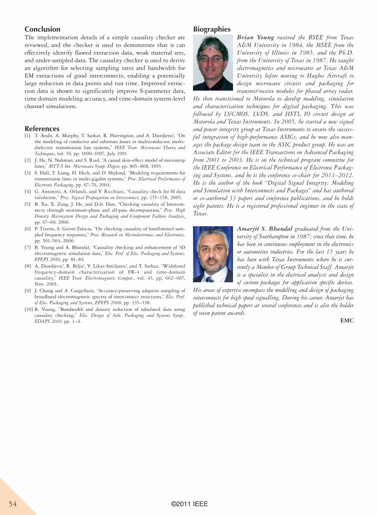
The last paper entitled, “A Simple Causality Checker and Its Use in Verifying, Enhancing, and Depopulating Tabulated Data from Electromagnetic Simulation,” is joint-ly authored by Brian Young and Amarjit S Bhandal from Texas Instruments USA and UK, respectively. With more powerful and accurate EM simulators available in the mar-ket, they become valuable tools for analyzing complex EMC problems. How do you know that the simulated results are correct, reliable, and usable? Causality check is one effective way to ensure that the simulated results are accurate and valid. Brian and Amarjit share with us the implementation details of a simple causality checker. The causality checker is used to derive an algorithm for selecting sampling rates and bandwidth for EM extractions of good interconnects, enabling a potentially large reduction in data points and run time. The improved extraction data has been shown to sig-nificantly improve S-parameter data and time domain simu-lation accuracy.
In conclusion, your active participation as authors and reviewers is needed so as to make this column a quality read. I wish you an enjoyable and fulfilling summer and feel free to share with me your feedback and comments, preferably by email at [email protected].
Easy Access to Pulsed Hertzian Dipole Fields Through Pole-Zero TreatmentTimothy J. Maloney, Intel Corporation, Santa Clara, CA; [email protected]
Abstract: The equations for EM dipole near and far radiation fields are formulated for the complex frequency domain with a Laplace Transform analysis for Hertzian dipoles. An s-domain pulsed current source function from ordinary circuit analysis is used in the expressions, and is augmented as needed to refine the pulse. This formulation allows a lucid pole-zero treatment of the field transfer function, yielding any field at any distance through the inverse Laplace Transform. Zeros of these expres-sions always include the “radiation zeros”, essential properties of the dipole fields themselves. Methods for recovery of current pulse waveforms from E- and H-field measurements, using filter functions, are described. The inverse Laplace Transform of
pole-zero expressions through Heaviside expansion is more accessible than ever through free web applets and commonly available software. Study of the small pulsed dipole has become important in semiconductor manufacturing, as engineers seek to monitor and control charged device model ESD events that could destroy components.
IntroductionDipole radiation is treated in many physics and engineering textbooks on electromagnetism (EM), only a few of which are cited here [1–3]. The most familiar treatment results in
expressions for the near and far fields is for the harmonic (sinu-soidal) source, but that is often generalized to the time-depen-dent dipole moment source, usually called p(t) for the electric dipole and m(t) for the magnetic dipole. The generalized time-dependent Hertzian (i.e., infinitesimal) dipole in free space will be useful for exploring pulsed fields. The complementary fea-tures of electric and magnetic dipole radiation and their E and H fields are well treated in EM textbooks, so we first will cen-ter the discussion on electric dipoles. Once the impact of the electric dipole moment p(t) and its time derivative on the fields is better understood, it will be clear how to apply these meth-ods to magnetic dipole radiation in the same way.
There are numerous motives for studying pulsed dipole radiation in free space, not least of which is an existing vast literature on antennas for pulsed applications. Many contem-porary works still refer to a landmark study from Caltech in 1974 called simply “Pulsed Antennas” [4], with 69 references and several lucid examples, beginning with the point source or Hertzian dipole. More recently, Schantz [5] studied the flow of electromagnetic power for pulsed Hertzian dipoles in the context of antenna design, and observed some interest-ing near and far field phenomena that relate to the present work, which will be discussed later. Atmospheric scientists who observe and often induce lightning strokes [6] have also produced a vast literature on pulsed fields; the present author hopes that this one reference could help lead the interested reader to more publications. While lightning is not an “infin-itesimal” source except at very far fields, researchers often start with the Hertzian dipole concept and may view lightning as a stack of such dipoles.
Another motivation to study pulsed dipole fields is closer to the present author’s interests, which include charged device model (CDM) electrostatic discharge (ESD) threats to semicon-ductor components. These phenomena have been known since the 1970s, and standardized tests have been formulated [7] to simulate the phenomena based on some well-designed equip-ment from the 1980s [8]. Radiation detection is not part of these semiconductor test activities, but it has been used to de-tect CDM events in the factory as part of a static control pro-gram [9]. More recently, semiconductor workers have looked more closely at the relation between CDM-like events and sig-nals from a nearby EMI-type antenna [10, 11]. Thus we have become highly interested in the fields produced by CDM pulses, including the strong near fields that a factory monitor antenna could pick up. The CDM test machine [7, 8] provides easy ac-cess to the current pulse information, so we would like to turn this into full, time-dependent near and far field information as easily as possible, using a Hertzian dipole approximation.
Figure 1 illustrates a familiar 3-axis scheme for electric di-pole radiation, showing the dipole (of presumed height dl) at the origin, and the names for Cartesian (x, y, z), spherical (r, u, f), and cylindrical (r, f, z) coordinates that may be used.
Transforming Dipole Field EquationsIf we pick and choose among textbook treatments of electric dipole time-dependent fields [1–3], we can formulate an expression in “practical” units for the most interesting field for electric dipole radiation, in terms of dipole moment p(t) and its first two time derivatives, the latter shown as p-dot and p-dou-ble-dot:
Eu 1 t 2 5sin u
4pe0a 3 p
$ 4c2r
13 p# 4cr2 1
3 p4r3 b . (1)
c is, of course, the speed of light and e0 the permittivity of free space. At all times the fields are understood to be delayed by the propagation time, so we will not be writing (t-r/c). There is also a radial E field and an azimuthal H field, but they do not con-tain all three terms in p(t), commonly called the static (p), inductive (p-dot) and far field radiative (p-double-dot) terms. We will treat these fields later. It is now clear that the pulsed field Eu is a maximum at the “equator” (sin u 5 1, where Eu and Ez are the same magnitude) and that full knowledge of the cur-rent I(t) plus the dipole moment length dl is sufficient to find p(t) and its derivatives, as p(t) 5 Q(t) ? dl, and I(t) 5 dQ(t)/dt.
How do we gain the promised “easy access” to these pulsed fields at all distances? Equation (1), in the context of current pulses beginning at time zero, is a perfect target for use of La-place Transforms [12], familiar to practitioners of electrical cir-cuit theory [13]. The use of Laplace Transforms (when named as such; we will avoid a digression on the near-equivalence of Fourier Transforms) for pulsed EM field problems seems to fall in and out of favor over the years. For example, in 1958 the well-respected physicist Paul I. Richards [14] used a Laplace Transform method and some very insightful coordinate trans-formations to look at pulsed EM waves in a conductive medium, seawater [15], without significant use of a computer. Despite such studies over the years showing the usefulness of Laplace Transforms in pulsed EM field problems, the present author has not been able to locate a simple Laplace Transform treatment of the pulsed Hertzian dipole in a popular EM textbook. But the Laplace Transform approach to pulsed (or even continuous wave) Hertzian dipole fields offers considerable insight into the phenomena and easy access to the fields for the engineer short on time and resources, so let us begin.
Equation (1) is transformed into to the Laplace (complex fre-quency; s 5 s 1 jv) domain by recalling [12] that the time derivative d/dt operator is s, and the integration operator is 1/s. This means that p(t) as above transforms to I(s)/s in the Laplace domain, and the time derivatives in (1) become s and s2. The propagation time to radius r is t 5 r/c so it can be a “constant” at a particular radius for the sake of an s-domain field equation. Eq. 1 can thus be expressed, very unusually, with 1/r3 factored out, and transformed into the s-domain as
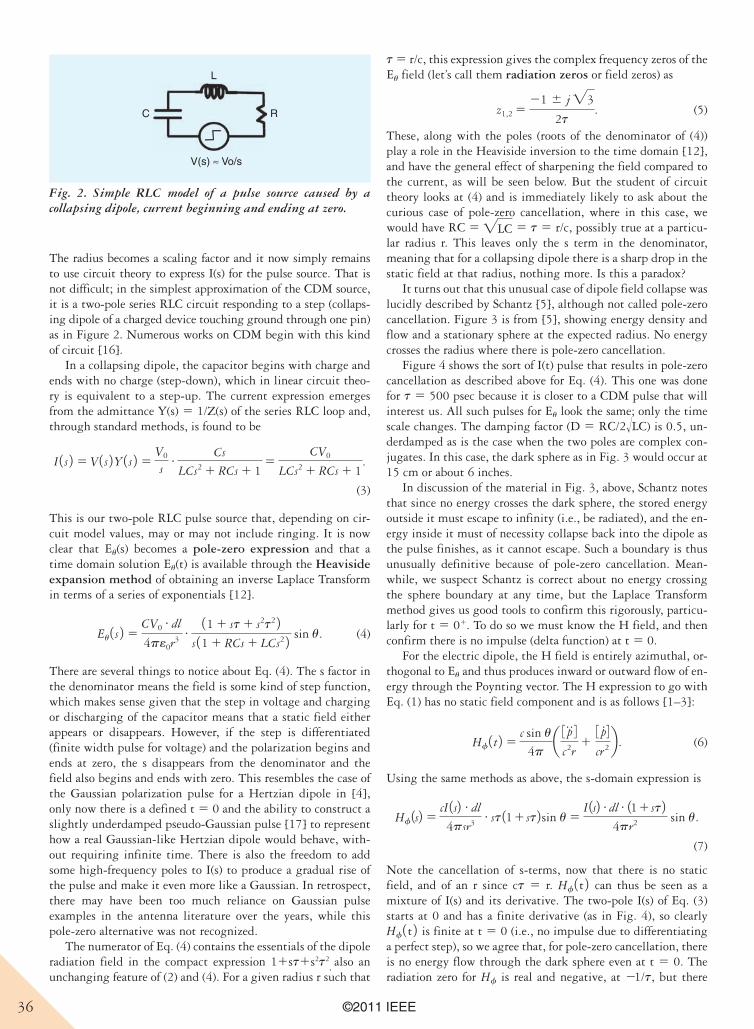
The radius becomes a scaling factor and it now simply remains to use circuit theory to express I(s) for the pulse source. That is not difficult; in the simplest approximation of the CDM source, it is a two-pole series RLC circuit responding to a step (collaps-ing dipole of a charged device touching ground through one pin) as in Figure 2. Numerous works on CDM begin with this kind of circuit [16].
In a collapsing dipole, the capacitor begins with charge and ends with no charge (step-down), which in linear circuit theo-ry is equivalent to a step-up. The current expression emerges from the admittance Y(s) 5 1/Z(s) of the series RLC loop and, through standard methods, is found to be
I 1 s 2 5 V 1 s 2Y 1 s 2 5V0
s# Cs
LCs2 1 RCs 1 15
CV0
LCs2 1 RCs 1 1.
(3)
This is our two-pole RLC pulse source that, depending on cir-cuit model values, may or may not include ringing. It is now clear that Eu(s) becomes a pole-zero expression and that a time domain solution Eu(t) is available through the Heaviside expansion method of obtaining an inverse Laplace Transform in terms of a series of exponentials [12].
Eu 1 s 2 5CV0
# dl
4pe0r3# 11 1 st 1 s2t2 2s 11 1 RCs 1 LCs2 2 sin u. (4)
There are several things to notice about Eq. (4). The s factor in the denominator means the field is some kind of step function, which makes sense given that the step in voltage and charging or discharging of the capacitor means that a static field either appears or disappears. However, if the step is differentiated (finite width pulse for voltage) and the polarization begins and ends at zero, the s disappears from the denominator and the field also begins and ends with zero. This resembles the case of the Gaussian polarization pulse for a Hertzian dipole in [4], only now there is a defined t 5 0 and the ability to construct a slightly underdamped pseudo-Gaussian pulse [17] to represent how a real Gaussian-like Hertzian dipole would behave, with-out requiring infinite time. There is also the freedom to add some high-frequency poles to I(s) to produce a gradual rise of the pulse and make it even more like a Gaussian. In retrospect, there may have been too much reliance on Gaussian pulse examples in the antenna literature over the years, while this pole-zero alternative was not recognized.
The numerator of Eq. (4) contains the essentials of the dipole radiation field in the compact expression 11st1s2t2
, also an
unchanging feature of (2) and (4). For a given radius r such that
t 5 r/c, this expression gives the complex frequency zeros of the Eu field (let’s call them radiation zeros or field zeros) as
z1,2 521 6 j "3
2t. (5)
These, along with the poles (roots of the denominator of (4)) play a role in the Heaviside inversion to the time domain [12], and have the general effect of sharpening the field compared to the current, as will be seen below. But the student of circuit theory looks at (4) and is immediately likely to ask about the curious case of pole-zero cancellation, where in this case, we would have RC 5 "LC 5 t 5 r/c, possibly true at a particu-lar radius r. This leaves only the s term in the denominator, meaning that for a collapsing dipole there is a sharp drop in the static field at that radius, nothing more. Is this a paradox?
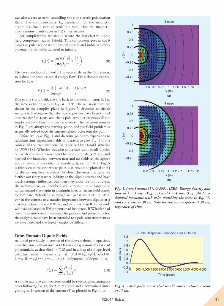
It turns out that this unusual case of dipole field collapse was lucidly described by Schantz [5], although not called pole-zero cancellation. Figure 3 is from [5], showing energy density and flow and a stationary sphere at the expected radius. No energy crosses the radius where there is pole-zero cancellation.
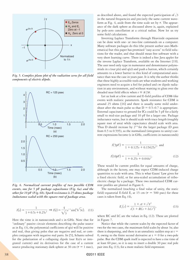
Figure 4 shows the sort of I(t) pulse that results in pole-zero cancellation as described above for Eq. (4). This one was done for t 5 500 psec because it is closer to a CDM pulse that will interest us. All such pulses for Eu look the same; only the time scale changes. The damping factor (D 5 RC/2!LC) is 0.5, un-derdamped as is the case when the two poles are complex con-jugates. In this case, the dark sphere as in Fig. 3 would occur at 15 cm or about 6 inches.
In discussion of the material in Fig. 3, above, Schantz notes that since no energy crosses the dark sphere, the stored energy outside it must escape to infinity (i.e., be radiated), and the en-ergy inside it must of necessity collapse back into the dipole as the pulse finishes, as it cannot escape. Such a boundary is thus unusually definitive because of pole-zero cancellation. Mean-while, we suspect Schantz is correct about no energy crossing the sphere boundary at any time, but the Laplace Transform method gives us good tools to confirm this rigorously, particu-larly for t 5 01. To do so we must know the H field, and then confirm there is no impulse (delta function) at t 5 0.
For the electric dipole, the H field is entirely azimuthal, or-thogonal to Eu and thus produces inward or outward flow of en-ergy through the Poynting vector. The H expression to go with Eq. (1) has no static field component and is as follows [1–3]:
Hf 1 t 2 5c sin u
4pa 3 p$ 4
c2r13 p# 4cr2b . (6)
Using the same methods as above, the s-domain expression is
Hf 1s2 5cI 1s2 # dl
4psr3# st 111 st2 sin u 5
I 1s2 # dl # 111 st24pr2 sin u.
(7)
Note the cancellation of s-terms, now that there is no static field, and of an r since ct 5 r. Hf 1 t 2 can thus be seen as a mixture of I(s) and its derivative. The two-pole I(s) of Eq. (3) starts at 0 and has a finite derivative (as in Fig. 4), so clearly Hf 1 t 2 is finite at t 5 0 (i.e., no impulse due to differentiating a perfect step), so we agree that, for pole-zero cancellation, there is no energy flow through the dark sphere even at t 5 0. The radiation zero for Hf is real and negative, at 21/t, but there
L
RC
V(s) ≈ Vo/s
Fig. 2. Simple RLC model of a pulse source caused by a collapsing dipole, current beginning and ending at zero.
was also a zero at zero, cancelling the s of electric polarization I(s)/s. The complementary Ef expression for the magnetic dipole also has a zero at zero, but recall that the magnetic dipole moment m(t) goes as I(s) times an area.
For completeness, we should record the last electric dipole field component, radial E-field. This component goes as cos u(peaks at polar regions) and has only static and inductive com-ponents, no 1/r fields radiated to infinity:
Er 1 t 2 5cos u
2pe0a 3 p
# 4cr2 1
3 p4r3 b . (8)
The cross product of Er with H is necessarily in the u direction, so it does not produce radial energy flow. The s-domain expres-sion for Er is
Er 1 s 2 5I 1 s 2 # dl
2pe0r3# 11 1 st 2cos u
s. (9)
Due to the static field, the s is back in the denominator. Er has the same radiation zero as Hf, at 21/t. The radiation zeros are shown in the complex plane in Figure 5. Students of circuit analysis will recognize that the field equations have been turned into transfer functions, and that a pole-zero plot expresses all the amplitude and phase information at once. The radiation zeros as in Fig. 5 are always the starting point, and the field problem is essentially solved once the current-related poles join the plot.
Before we leave Fig. 5 and do some pole-zero expansions to calculate time-dependent fields, it is useful to view Fig. 5 in the context of the “radiansphere” as described by Harold Wheeler in 1959 [18]. Wheeler was also concerned with small dipoles but with continuous wave (cw) harmonic signals (s 5 jv), and marked the boundary between near and far fields as the sphere with a radius of one radian of wavelength, i.e., vt 5 1. Fig. 5 is thus seen as the case where poles 6jv would be plotted at 6j for the radiansphere boundary. At closer distances, the zeros are further out (they start at infinity at the dipole source) and have much stronger influence, but then they cross the unit circle at the radiansphere, as described, and continue on at larger dis-tances toward the origin in a straight line, as the far field comes to dominate. Wheeler also recognized (what we call) 1 1 st 1 s2t2
in the context of a transfer impedance between dipoles at a
distance defined by our t 5 r/c, and in terms of an RLC network with values based on EM properties of free space. If Wheeler had been more interested in complex frequencies and pulsed dipoles, the analysis could have been extended to a pole-zero treatment as we have here, and the history might be different.
Time-Domain Dipole FieldsAs noted previously, inversion of the above s-domain equations into the time domain involves Heaviside expansion of a ratio of polynomials, as described in [12] and in a host of college-level calculus texts. Essentially, if f 1s2 5 p 1s2 /q 1s2 , q 1 s 2 51s2 a12 1s2a22c1s2am2 , p 1 s 2 a polynomial of degree , m,
F 1 t 2 5 am
n51
p 1an 2q r 1an 2 e
ant. (10)
A simple example with no zeros would be two complex conjugate poles following Eq. (5) for t 5 500 psec and a normalized (inte-grating to 1) version of the current (3) as plotted in Fig. 4, or
Here the time is in nanoseconds and s in GHz. Note that for “ordinary” passive circuit elements describing the pulse source as in Eq. (3), the polynomial coefficients of q(s) will be positive and real, thus giving poles that are negative and real, or com-plex conjugates with negative real parts. In [5], Schantz solved for the polarization of a collapsing dipole (our I(s)/s or inte-grated current) and its derivatives for the case of a current source producing stationary dark sphere at 30 cm (t 5 1 nsec),
as described above, and found the expected participation of !3 in the natural frequencies and precisely the same current wave-form as Fig. 4, aside from the time scale set by t. The appear-ance of the dark sphere as discussed above is, again, explained by pole-zero cancellation at a critical radius. Now let us try some field calculations.
Inverting Laplace Transforms through Heaviside expansion can be done with one- or two-line commands on a computer. Many software packages do this (the present author uses Math-ematica) but this paper has promised “easy access” to field solu-tions for the reader, and that should mean free software with a very short learning curve. There is indeed a free Java applet for the inverse Laplace Transform, available on the Internet [19]. The user need only type in numerator and denominator polyno-mials in s (our p(s) and q(s)) and push a button, which certainly amounts to a lower barrier to this kind of computational assis-tance than was the case in years past. It is why the author thinks that these highly accessible tools are what students and working engineers need to acquire a feel for pulsed and cw dipole radia-tion in any environment, and without wanting to gloss over the dreaded near field effects when r # l/2p.
Let us look at a few current and E-field profiles of CDM-like events with realistic parameters. Spark resistance for CDM is around 25 ohms [16] and there is usually some mild under-shoot after the main pulse so that D 5 0.5–0.7 is appropriate. External capacitance to ground for ICs could be 5 pF for a fairly small to mid-size package and 10 pF for a larger one. Package inductance varies, but it should scale with trace length (roughly square root of area) while capacitance should scale with area. Thus D should increase by 21/4
for the larger package (D goes
from 0.5 to 0.595), so the normalized (integrates to unity) cur-rent expressions become (s in GHz, coefficients in nanoseconds)
I 15pF 2 51
1 1 0.125s 1 0.15625s2, and
I 110pF2 51
1 1 0.25s 1 0.044s2. (12)
These would be current profiles for equal amounts of charge, although in the factory, one may expect CDM-induced charge quantities to scale with area. This is what Gauss’ Law gives for a fixed electric field, or for area-scaled accumulation of tribo-electric charge by a package. These two normalized CDM cur-rent profiles are plotted in Figure 6.
The normalized (reaching a final value of unity, the static field) equatorial E-field Ez at 15 cm (t 5 500 psec) for these cases is taken from Eq. (4),
Ez 1 s 2 51 1 st 1 s2t2
s 11 1 RCs 1 LCs2 2 , (13)
where RC and LC are the values in Eq. (12). These are plotted in Figure 7.
Notice that while the current scales by the expected factor of two for the two cases, the maximum field scales by about 3x; also there is sharpening, and there is an unrealistic sudden step at t 5 0, owing to the finite second derivative at t 5 0 for a two-pole pulse. But the CDM spark itself is expected to have a rise time of at least 60 psec, so it is easy to insert a double 30 psec real pole pair into Eq. (13), for a more realistic field expression:
j y
x
e j 4π /3
e j 2π /3
–1
Normalizedto 1/τ
Eθ Zeros
Hφ and ErZero at –1 Hφ Zero at 0
Fig. 5. Complex plane plot of the radiation zeros for all field components of electric dipole.
0.5
1.0
1.5
2.0
0.5 1.0 1.5 2.0
1
2
3
4
Time (nsec)
0.5 1.0 1.5 2.0Time (nsec)
(a)
(b)
RC = 125 psec
RC = 250 psec
Fig. 6. Normalized current profiles of two possible CDM events, one for 5 pF package capacitance (Fig. 6a) and the other for 10 pF (Fig. 6b). Spark resistance is 25 ohms; package inductance scaled with the square root of package area.
These easily calculated CDM E-fields are shown in Figure 8. As noted earlier, the charge-up case is equivalent to charge-
down, so CDM pulse fields would ordinarily be shifted down (by 21 for these normalized pulses) to show zero field at steady state.
In the more realistic case of Fig. 8, the E-field amplitude swing is still about 3x more for the faster device, which has 2x the peak current and equal charge compared to the other. Because of the derivatives (in the radiation polynomials of Eqs. 13–14), fields are definitely sharper and of shorter time duration than the current of Fig. 6, even after the spark rise time is added; the spark rise time affects the startup phase of the pulses. At 15 cm, the slower 250 psec 5 RC pulse in Fig. 8b is clearly more in the near field zone because of its lower frequency content, meaning that the final static field Ez 5 1 is fairly large compared to transient fields.
Before we look at field measurement, let us calculate a tran-sient magnetic field. Going back to the collapsing dipole exam-ple of Schantz [5] at the dark sphere at 30 cm, we decided that ExH integrated over time has to be zero at that radius, although there is a finite magnetic field as the electric field steps down suddenly. Now employing the radiation zeros for Hf, the nor-malized equatorial field, following Eq. (7) and with GHz units for s and nanoseconds for t, is
Hf 1 s 2 5I 1 s 2
s# s 11 1 st 2 5
1 1 st
1 1 st 1 s2t2 51 1 s
1 1 s 1 s2,
for t 5 1 nsec. (15)
Hf 1 t 2 is plotted in Figure 9, calculated from the inverse Laplace Transform web Java applet [19].
Because of the finite second derivative of I(t) in the two-pole form, the Hf field has a pure step at t 5 0. But because the finite ExH lasts for zero time, no energy is transmitted across the dark
6
5
4
3
2
1
0
1
0.5 1.0 1.5 2.0
5
10
15
Time (nsec)
0.5 1.0 1.5 2.0Time (nsec)
(a)
(b)
RC = 125 psec
RC = 250 psec
Fig. 7. Normalized vertical E-fields for the current profiles in Fig. 6.
4
3
2
1
0.5 1.0 1.5 2.0
4
2
–2
6
8
Time (nsec)
0.5 1.0 1.5 2.0Time (nsec)
(a)
(b)
RC = 125 psec
RC = 250 psec
Fig. 8. Normalized vertical E-fields as described by Eq. (14), with extra double pole for 60 psec spark rise time. Peak-peak amplitude is almost 3x greater for the smaller, faster device in Fig. 8a.
Fig. 9. Inversion of Eq. (15) to give Hf(t), using web applet
[19]. Time scale in nanoseconds; expression is normalized to give integral of unity.
sphere. However, the E-field at all radii also has a t 5 0 step as in Fig. 7, which led us to the spark rise time poles of Eq. (14) and the more realistic fields of Fig. 8. Such rise time poles would remove the pure steps from E and H fields at the dark sphere and introduce a small but finite ExH energy flow during the spark rise time.
Field Measurement and the Goal of Current ImagingWe will now briefly discuss transient field detection, and how it applies to the foregoing calculations and some related practi-
cal situations for EMC and ESD engineers. E and H field detec-tion is of course a vast subject, so we will cover only a few high points here, and defer a more complete discussion of transient field measurements to a future article.
No discussion of ESD-created transient fields as created by Hertzian dipoles would be complete without citing Wilson and Ma [20], a work now over 20 years old. Using a broad-band horn antenna for E-fields, and an ESD pulser gun resem-bling one that would now be compliant with IEC 61000-4-2, the authors measured and compared pulse currents and radi-ated fields. Field results seemed most successful for measure-ments at 150 cm distance from the pulser gun and, to this reader, the minor discrepancies in theory vs. experiment were largely cleared up by some work published in 2007 [21] that included Microwave Studio (MWS) computer simulations. Caniggia and Maradei [21] found substantial effect of the re-turn path of the current, which depends on gun strap place-ment and is even frequency-dependent. Nonetheless, at 150 cm distance from the source, there is now some case for view-ing the current pulse as, primarily, a magnetic dipole. Note that with a magnetic dipole, the dipole moment goes as I(s) instead of I(s)/s, and that, mirroring the H field for electric dipole radiation, there is no long-term static electric field. In short, the extra derivative of the magnetic dipole model leads to a reasonably good fit of the E-field profile as measured at 150 cm in [20], including the undershoot, when combined with a simple model (double exponential plus step) for the current as measured at the target. The foregoing is a nearly ideal application of the Laplace Transform field calculation methods described above, and would make a fine homework assignment for students and engineers trying to learn about transient fields. We hope the authors of [20] understand that this is the benefit of hindsight, and the much later efforts of [21] and a result of perhaps other works that led to a more complete understanding. Even so, it appears that the dipole radiation model is still meaningful.
We do not always have a broadband TEM horn antenna with flat frequency response for measuring E-fields, as in [20]. Something smaller is needed in practical manufacturing situa-tions, where a small near field antenna is required [9]. Conve-niently, Caniggia and Maradei [21] also discuss basic E-field and H-field probes and their agreement with simple theory. The E-field monopole probe (coaxial cable with extended center conductor) agrees remarkably well with a two-pole, one zero RLC model for the transfer function. Using the notation of the present article, the measured signal as compared to vertical E-field is essentially
Vm 1 s 2Ez 1 s 2 5
lmZ0Cms
1 1 Z0Cms 1 LmCms2, (16)
for which Z0 is cable impedance (usually 50 ohms), Cm and Lm are the inductive and capacitive equivalents of the probe wire, and lm is the length of the probe wire. Model parameters can be calculated as described in [21] and cited earlier references [22], although it has long been known that the exact solution is a little more complicated [23]. The result for a 6 mm monopole probe as in [21] is a very good dE/dt probe up to 1 GHz or so, and not too severe a departure from the simple model of Eq. (16) beyond that. Such models enhance our pros-pects for recovering the current I(s) and I(t) (i.e., current imaging) through filtering of the measured field signal. For
1 2 3 4 5 6 7–0.2
0.2
0.4
0.6
0.8
1.0
Time (nsec)
Fig. 10. Normalized filter function impulse response, as in Eq. (17), for a small E-probe. Z0Cm = 25.2 psec, LmCm = 541.6 (psec)2 , r = 15 cm. For these values, there is also a very small Dirac delta function (0.002) at the origin that brings the integral to unity. This function would be convolved (e.g., with free tools as in [24]) with the measured field signal Vm(t) to produce an image of the time-dependent source current I(t).
0.2 0.4 0.6 0.8 1.0 1.2 1.4
–50
50
100
150
–10
10
20
30
40
50
Time (nsec)
0.2 0.4 0.6 0.8 1.0 1.2 1.4Time (nsec)
(a)
(b)
RC = 250 psec
RC = 125 psec
Fig. 11. Normalized E-field signals, predicted for measurement at 15 cm using the E-probe transfer function in Eq. (16) as described for Fig. 10. For equal charge, the smaller device (5 pF, Fig. 10a) has about 3x the peak-peak voltage swing (Vp-p) of the larger (10 pF) device.
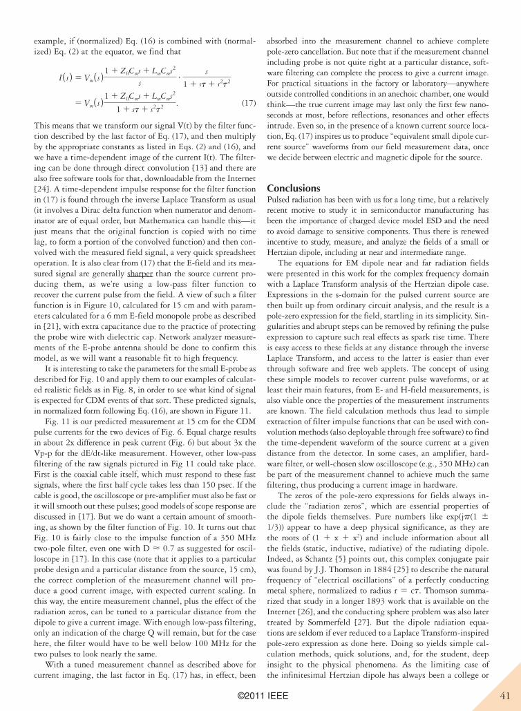
example, if (normalized) Eq. (16) is combined with (normal-ized) Eq. (2) at the equator, we find that
I 1 s 2 5 Vm 1 s 2 1 1 Z0Cms 1 LmCms2
s# s
1 1 st 1 s2t2
5 Vm 1 s 2 1 1 Z0Cms 1 LmCms2
1 1 st 1 s2t2 . (17)
This means that we transform our signal V(t) by the filter func-tion described by the last factor of Eq. (17), and then multiply by the appropriate constants as listed in Eqs. (2) and (16), and we have a time-dependent image of the current I(t). The filter-ing can be done through direct convolution [13] and there are also free software tools for that, downloadable from the Internet [24]. A time-dependent impulse response for the filter function in (17) is found through the inverse Laplace Transform as usual (it involves a Dirac delta function when numerator and denom-inator are of equal order, but Mathematica can handle this—it just means that the original function is copied with no time lag, to form a portion of the convolved function) and then con-volved with the measured field signal, a very quick spreadsheet operation. It is also clear from (17) that the E-field and its mea-sured signal are generally sharper than the source current pro-ducing them, as we’re using a low-pass filter function to recover the current pulse from the field. A view of such a filter function is in Figure 10, calculated for 15 cm and with param-eters calculated for a 6 mm E-field monopole probe as described in [21], with extra capacitance due to the practice of protecting the probe wire with dielectric cap. Network analyzer measure-ments of the E-probe antenna should be done to confirm this model, as we will want a reasonable fit to high frequency.
It is interesting to take the parameters for the small E-probe as described for Fig. 10 and apply them to our examples of calculat-ed realistic fields as in Fig. 8, in order to see what kind of signal is expected for CDM events of that sort. These predicted signals, in normalized form following Eq. (16), are shown in Figure 11.
Fig. 11 is our predicted measurement at 15 cm for the CDM pulse currents for the two devices of Fig. 6. Equal charge results in about 2x difference in peak current (Fig. 6) but about 3x the Vp-p for the dE/dt-like measurement. However, other low-pass filtering of the raw signals pictured in Fig 11 could take place. First is the coaxial cable itself, which must respond to these fast signals, where the first half cycle takes less than 150 psec. If the cable is good, the oscilloscope or pre-amplifier must also be fast or it will smooth out these pulses; good models of scope response are discussed in [17]. But we do want a certain amount of smooth-ing, as shown by the filter function of Fig. 10. It turns out that Fig. 10 is fairly close to the impulse function of a 350 MHz two-pole filter, even one with D < 0.7 as suggested for oscil-loscope in [17]. In this case (note that it applies to a particular probe design and a particular distance from the source, 15 cm), the correct completion of the measurement channel will pro-duce a good current image, with expected current scaling. In this way, the entire measurement channel, plus the effect of the radiation zeros, can be tuned to a particular distance from the dipole to give a current image. With enough low-pass filtering, only an indication of the charge Q will remain, but for the case here, the filter would have to be well below 100 MHz for the two pulses to look nearly the same.
With a tuned measurement channel as described above for current imaging, the last factor in Eq. (17) has, in effect, been
absorbed into the measurement channel to achieve complete pole-zero cancellation. But note that if the measurement channel including probe is not quite right at a particular distance, soft-ware filtering can complete the process to give a current image. For practical situations in the factory or laboratory—anywhere outside controlled conditions in an anechoic chamber, one would think—the true current image may last only the first few nano-seconds at most, before reflections, resonances and other effects intrude. Even so, in the presence of a known current source loca-tion, Eq. (17) inspires us to produce “equivalent small dipole cur-rent source” waveforms from our field measurement data, once we decide between electric and magnetic dipole for the source.
ConclusionsPulsed radiation has been with us for a long time, but a relatively recent motive to study it in semiconductor manufacturing has been the importance of charged device model ESD and the need to avoid damage to sensitive components. Thus there is renewed incentive to study, measure, and analyze the fields of a small or Hertzian dipole, including at near and intermediate range.
The equations for EM dipole near and far radiation fields were presented in this work for the complex frequency domain with a Laplace Transform analysis of the Hertzian dipole case. Expressions in the s-domain for the pulsed current source are then built up from ordinary circuit analysis, and the result is a pole-zero expression for the field, startling in its simplicity. Sin-gularities and abrupt steps can be removed by refining the pulse expression to capture such real effects as spark rise time. There is easy access to these fields at any distance through the inverse Laplace Transform, and access to the latter is easier than ever through software and free web applets. The concept of using these simple models to recover current pulse waveforms, or at least their main features, from E- and H-field measurements, is also viable once the properties of the measurement instruments are known. The field calculation methods thus lead to simple extraction of filter impulse functions that can be used with con-volution methods (also deployable through free software) to find the time-dependent waveform of the source current at a given distance from the detector. In some cases, an amplifier, hard-ware filter, or well-chosen slow oscilloscope (e.g., 350 MHz) can be part of the measurement channel to achieve much the same filtering, thus producing a current image in hardware.
The zeros of the pole-zero expressions for fields always in-clude the “radiation zeros”, which are essential properties of the dipole fields themselves. Pure numbers like exp(jp(1 6 1/3)) appear to have a deep physical significance, as they are the roots of (1 1 x 1 x2) and include information about all the fields (static, inductive, radiative) of the radiating dipole. Indeed, as Schantz [5] points out, this complex conjugate pair was found by J.J. Thomson in 1884 [25] to describe the natural frequency of “electrical oscillations” of a perfectly conducting metal sphere, normalized to radius r 5 ct. Thomson summa-rized that study in a longer 1893 work that is available on the Internet [26], and the conducting sphere problem was also later treated by Sommerfeld [27]. But the dipole radiation equa-tions are seldom if ever reduced to a Laplace Transform-inspired pole-zero expression as done here. Doing so yields simple cal-culation methods, quick solutions, and, for the student, deep insight to the physical phenomena. As the limiting case of the infinitesimal Hertzian dipole has always been a college or
graduate student’s starting point for serious consideration of ra-diation, good interactive tools for developing insight are help-ful. Now that we find the small pulsed dipole has remarkable significance for observed CDM radiation, as above, we also need simple, accessible tools for busy working engineers to use for comprehending these practical problems, and thus the methods described in this work were developed.
The author always found the use of “jv” in EM-related books to be a bit restrictive, having learned the “secret” of the La-place Transform and complex frequencies as a college sopho-more. He felt free to let jv 5 s on most occasions when reading those books, as the expressions would seem a bit simpler, while also becoming more general. The s-domain expressions in this paper are a good example of that practice, one that brought unusual clarity to the subject under study. The author contin-ues to cross-check as many EM problems as possible with the s-domain approach, using field equations as expressed in this work. Somehow, the “bookkeeping” of the various fields and their r-dependence is more tractable. Consider, for example, the physics examples of Prof. K.T. McDonald of Princeton Univer-sity [28]. If, like the author, you have often searched the Inter-net for information on EM problems, you have undoubtedly encountered Prof. McDonald’s examples and articles, multiple times. Some of his EM examples are admittedly incomplete, i.e., works in progress. Reformulating the EM dipole equations and current sources in Laplace Transform format can be quite revealing, at least when there is a defined beginning at t 5 0. Indeed, it was not a field problem but an incomplete capacitor problem posed by McDonald and solved by both of us in 2008 [29] that convinced the author that more Laplace Transform analysis is needed to understand and solve ESD problems. After all, ESD is a pulse that begins at time zero.
References[1] S. Ramo, J. Whinnery, and T. Van Duzer, Fields and Waves in Communica-
tion Electronics (New York: John Wiley & Sons, 1965).[2] J.B. Marion, Classical Electromagnetic Radiation (New York: Academic Press,
1965).[3] J. D. Jackson, Classical Electrodynamics, 3rd Edition (New York: John Wiley
and Sons, 1999).[4] G. Franceschetti and C.H. Papas, “Pulsed Antennas”, IEEE Trans. on Anten-
nas and Propagation, Vol. AP-22, No. 5, Sept. 1974, pp. 651–661. [5] H.G. Schantz, “Electromagnetic Energy Around Hertzian Dipoles”, IEEE
Antenna & Prop. Magazine, Vol. 43 (2) April 2001, pp. 50–62.[6] M.A. Uman, J. Schoene, V. A. Rakov, K. J. Rambo, and G. H. Schnetzer,
“Correlated Time Derivatives of Current, Electric Field Intensity, and Magnetic Flux Density for Triggered Lightning at 15 m”, Journal of Geo-physical Research, Vol. 107, No. D13, 2002, pp. 1–11.
[7] JEDEC JESD22-C101-C standard, “Field-Induced Charged-Device Model Test Method for Electrostatic-Discharge-Withstand Thresholds of Micro-electronic Components”, Dec. 2004. See www.jedec.org.
[8] R. Renninger, M-C. Jon, D.L. Lin, T. Diep and T.L. Welsher, “A Field-Induced Charged-Device Model Simulator”, EOS/ESD Symposium Proceed-ings, 1989, pp. 59–71.
[9] J.A. Montoya and T.J. Maloney, “Unifying Factory ESD Measurements and Component ESD Stress Testing”, EOS/ESD Symposium Proceedings, 2005, pp. 229–237.
[10] A. Jahanzeb, K. Wang J. Harrop, J. Brodsky, T. Ban, S. Ward, J. Schichl, K. Burgess, C. Duvvury, “’Real World’ Discharge Event Detection”, 2011 International ESD Workshop, Lake Tahoe, CA, May 2011 (to be published).
[11] A. Jahanzeb, K. Wang J. Harrop, J. Brodsky, T. Ban, S. Ward, J. Schichl, K. Burgess, C. Duvvury, “Capturing Real World ESD Stress with Event Detec-tor”, 2011 EOS/ESD Symposium, Anaheim, CA, Sept. 2011 (to be published).
[12] M. Abramowitz and I.A. Stegun, Handbook of Mathematical Functions, (New York: Dover Publications, 1965).
[13] R.N. Bracewell, The Fourier Transform and Its Applications, (New York: McGraw-Hill, 1965).
[14] R. Levy and S.B. Cohn, “A History of Microwave Filter Research, Design, and Development”, IEEE Trans. on Microwave Theory and Techniques, vol. MTT-32, no. 9, Sept. 1984, pp. 1055–1067. “Richards…had a brilliant career both as an engineer and as a physicist, and was well known for many fine contributions in the fields of physics and applied mathematics.”
[15] P.I. Richards. “Transients in Conducting Media”, IRE Trans. on Antennas and Propagation, April 1958, pp. 178–182.
[16] B. Atwood, Y. Zhou, D. Clarke, T. Weyl, “Effect of Large Device Capacitance on FICDM Peak Current”, EOS/ESD Symposium Proceedings, 2007, pp. 275–82.
[17] C. Mittermayer and A. Steininger, “On the Determination of Dynamic Errors for Rise Time Measurement with an Oscilloscope”, IEEE Trans. on Instrumentation and Measurement, Vol. 48, no. 6, Dec. 1999, pp. 1103–07.
[18] H.A. Wheeler, “The Radiansphere Around a Small Antenna”, Proceedings of the IRE, vol. 47, 1959, pp. 1325–1331.
[19] Web resource, http://www.eecircle.com/applets/007/ILaplace.html.[20] P.F. Wilson and M.T. Ma, “Fields Radiated by Electrostatic Discharges,”
IEEE Trans. on Electromagnetic Compatibility, vol. 33, no.1, Feb 1991, pp.10–18.[21] S. Caniggia and F. Maradei, “Numerical Prediction and Measurement of
ESD Radiated Fields by Free-Space Field Sensors”, IEEE Trans. on Electro-magnetic Compatibility, vol. 49, no. 3, Aug. 2007, pp. 494–503.
[22] S. A. Schelkunoff and H. T. Friis, Antennas: Theory and Practice (New York: Wiley, 1952).
[23] C.W. Harrison, “The Radian Effective Half-length of Cylindrical Anten-nas Less Than 1.3 Wavelengths Long”, IEEE Trans. on Antennas and Propa-gation, 1963, AP-11, (6), pp. 657–660.
[24] Web resource, “Excellaneous” Visual Basic macros for Excel, at http://www.bowdoin.edu/~rdelevie/excellaneous/#downloads.
[25] J.J. Thomson, “On Electrical Oscillations and the effects produced by the motion of an Electrified Sphere”, Proc. London Math. Society, April 8, 1884, pp. 197–218.
[26] J.J. Thomson, J.C. Maxwell, Notes on Recent Researches in Electricity and Mag-netism: intended as a sequel to Prof. Clerk Maxwell’s Treatise on Electricity and Magnetism, 1893, p. 370. Free Google e-Book; http://books.google.com.
[27] A. Sommerfeld, Electrodynamics, (New York: Academic Press, 1952) pp. 154–155.
[28] Web site: http://puhep1.princeton.edu/~mcdonald/examples/. [29] Web article, Kirk T. McDonald and Timothy J. Maloney, “Leaky Capaci-
BiographyTimothy J. Maloney received an S.B. degree in physics from the Massachusetts Institute of Technol-ogy in 1971, an M.S. in physics from Cornell University in 1973, and a Ph.D. in electrical engineering from Cornell in 1976, where he was a National Science Foundation Fellow. He was a Postdoctoral Associate at Cornell until 1977, when he joined the Central Research Laboratory of
Varian Associates, Palo Alto, CA. At Varian until 1984, he worked on III-V semiconductor photocathodes, solar cells and microwave devices, as well as silicon molecular beam epitaxy and MOS process technology. Since 1984 he has been with Intel Corp., Santa Clara, CA, where he has been concerned with integrated circuit electrostatic discharge (ESD) protection and testing, CMOS latchup, fab process reliability, signal integrity, and system ESD testing, including cable discharge. His papers at the 2008 and 2010 EMC Symposium relate to system ESD tests. He is now a Senior Principal Engineer at Intel. He has received the Intel Achievement Award for his patented ESD protection devices, which have achieved breakthrough ESD performance enhancements for a wide variety of Intel products. He now holds thirty-two patents, with several more pending.
Dr. Maloney received Best Paper Awards for his contributions to the EOS/ESD Symposium in 1986 and 1990, was General Chairman for the 1992 EOS/ESD Symposium, and received the ESD Associa-tion’s Outstanding Contributions Award in 1995. He has taught short courses at UCLA, University of Wisconsin, and UC Berkeley. He is co-author of a book, “Basic ESD and I/O Design” (Wiley, 1998), and is a Fellow of the IEEE. EMC
Physical Dimensions vs Electrical DimensionsClayton R. Paul, Mercer University, Macon, GA (USA), [email protected]
Abstract – With the operating frequencies of today’s high-speed digital and high-frequency analog systems increasing, previous lumped-circuit analysis methods will no longer be valid and will give incorrect answers. When the maximum physical dimensions of the system are electrically large (greater than a tenth of a wavelength) the system cannot be reliability analyzed using Kirchhoff’s voltage and current laws and lumped-circuit methods.
I. Deficiencies With The Exclusive Use of Kirchhoff’s Laws and Lumped-Circuit ModelsThe spectral (frequency) content of modern high-speed digital waveforms today is extending into the GHz regime. Similarly, the operating frequencies of analog systems are extending well into the GHz range. A digital clock waveform has a trapezoidal shape as illustrated in Fig. 1:
Since a digital clock waveform is a periodic, repetitive waveform, according to the Fourier series their time-domain waveforms can be alternatively viewed as being composed of an infinite number of harmonically related sinusoidal components as [1]
x 1 t 2 5 c0 1 c1 cos 1v0t 1 u12 1 c2 cos 12v0t 1u221 c3 cos 13v0t 1 u32 1c
5 c0 1a`
n51
cn cos1nv0t1un2 (1)
The period T of the periodic waveform is the reciprocal of the clock fundamental frequency, f0, and the fundamental radian frequency is v0 5 2p f0. The rise/fall times are denoted as tr
and tf, respectively, and the pulse width (between 50% levels) is denoted as t. As the fundamental frequencies of the clocks, f0, are increased, their period T 5 1@f0
decreases and hence the rise/fall times of the pulses must be reduced commensurately in order that pulses resemble a trapezoidal shape rather than a “saw tooth” waveform thereby giving adequate “setup” and “hold” time intervals. Reducing the pulse rise/fall times has had the consequence of increasing the spectral content of the wave shape. Typically this spectral content is significant up to the inverse of the rise/fall times, 1@tr
. For example, a 1 GHz digital clock signal having rise/fall times of 100ps has signifi-cant spectral content at multiples (harmonics) of the basic clock frequency (1 GHz, 2 GHz, 3 GHz, …..) up to around 10 GHz.
In the past, clock speeds and data rates of digital systems were in the megahertz (MHz) range with rise/fall times of the pulses in the nanosecond (1ns 5 1029s) range. Prior to that time, the “lands” (conductors of rectangular cross section) that interconnect the electronic modules on printed circuit boards (PCBs) had little effect on the proper functioning of those elec-tronic circuits. The time delays through the modules domi-nated the time delay imposed by the interconnect conductors.
Today, the clock and data speeds have rapidly moved into the low gigahertz (GHz) range. The rise/fall times of those digital waveforms have decreased into the picosecond (1ps 5 10212s) range. The delays of the interconnects have become the domi-nant factor.
Although the “physical lengths” of the lands that intercon-nect the electronic modules on the PCBs have not changed sig-nificantly over these intervening years, their “electrical lengths” (in wavelengths) have increased dramatically because of the in-creased spectral content of the signals that the lands carry. To-day these “interconnects” can have a significant effect on the signals they are carrying so that just getting the systems to work properly has become a major design problem. Remember that it does no good to write sophisticated software if the hard-ware cannot faithfully execute those instructions. This has gen-erated a new design problem referred to as Signal Integrity. Good signal integrity means that the interconnect conductors (the lands) should not adversely affect the operation of the modules that the conductors interconnect. Because these interconnects are becoming “electrically long”, lumped-circuit modeling of them is becoming inadequate and gives erroneous answers. The interconnect conductors must now be treated as distributed-circuit transmission lines.
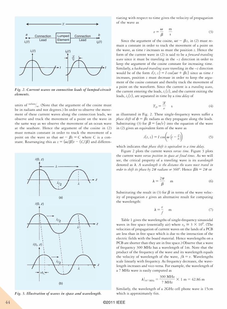
II. Traveling Waves, Time Delay and WavelengthIn the analysis of electric circuits using Kirchhoff’s voltage and current laws and lumped-circuit models, we ignored the connec-tion leads attached to the lumped elements. When is this per-missible? Consider a lumped-circuit element having attachment leads of total length l shown in Fig. 2. Single-frequency, sinusoi-dal currents along the attachment leads are in fact traveling waves which can be written in terms of position z along the leads and time t as
i 1 t, z 2 5 Icos 1vt 2 bz 2 (2)
where the radian frequency v is written in terms of cyclic frequency f as v 5 2p f radians@s and b is the phase constant in
units of radians@m. (Note that the argument of the cosine must be in radians and not degrees.) In order to observe the move-ment of these current waves along the connection leads, we observe and track the movement of a point on the wave in the same way as we observe the movement of an ocean wave at the seashore. Hence the argument of the cosine in (2) must remain constant in order to track the movement of a point on the wave so that vt 2 bz 5 C where C is a con-stant. Rearranging this as z 5 1v/b2 t 2 1C/b 2 and differen-
tiating with respect to time gives the velocity of propagation of the wave as
v 5v
b
ms
(3)
Since the argument of the cosine, vt 2 bz, in (2) must re-main a constant in order to track the movement of a point on the wave, as time t increases so must the position z. Hence the form of the current wave in (2) is said to be a forward-traveling wave since it must be traveling in the +z direction in order to keep the argument of the cosine constant for increasing time. Similarly, a backward-traveling wave traveling in the –z direction would be of the form i 1 t, z 2 5 I cos 1vt 1 bz 2 since as time t increases, position z must decrease in order to keep the argu-ment of the cosine constant and thereby track the movement of a point on the waveform. Since the current is a traveling wave, the current entering the leads, i1 1 t 2 , and the current exiting the leads, i2 1 t 2 , are separated in time by a time delay of
TD 5lv s (4)
as illustrated in Fig. 2. These single-frequency waves suffer a phase shift of f 5 bz radians as they propagate along the leads. Substituting (3) for b 5 1v/v 2 into the equation of the wave in (2) gives an equivalent form of the wave as
i 1 t, z 2 5 I cosav Qt 2zv Rb (5)
which indicates that phase shift is equivalent to a time delay.Figure 2 plots the current waves versus time. Figure 3 plots
the current wave versus position in space at fixed times. As we will see, the critical property of a traveling wave is its wavelengthdenoted as l. A wavelength is the distance the wave must travel in order to shift its phase by 2p radians or 360o. Hence bl 5 2p or
l 52p
b m (6)
Substituting the result in (3) for b in terms of the wave veloc-ity of propagation v gives an alternative result for computing the wavelength:
l 5v
f m (7)
Table 1 gives the wavelengths of single-frequency sinusoidal waves in free space (essentially air) where v0 > 3 3 108. (The velocities of propagation of current waves on the lands of a PCB are less than in free space which is due to the interaction of the electric fields with the board material. Hence wavelengths on a PCB are shorter than they are in free space.) Observe that a wave of frequency 300 MHz has a wavelength of 1m. Note that the product of the frequency of the wave and its wavelength equals the velocity of wavelength of the wave, fl 5 v. Wavelengths scale linearly with frequency. As frequency decreases, the wave-length increases and vice-versa. For example, the wavelength of a 7 MHz wave is easily computed as
l 0 @7 MHz 5300 MHz
7 MHz3 1 m 5 42.86 m
Similarly, the wavelength of a 2GHz cell phone wave is 15cm which is approximately 6in.
a
i1(t )
i1(t )
i2(t )
i2(t )
ConnectionLead
ConnectionLead
LumpedElement
b
lυ
t t
l
Fig. 2. Current waves on connection leads of lumped-circuit elements.
i (0, z )
i (0, z )
i (t1, z )
νt1
λ
λ
λ
λ
λ 2
λ 2
λ 2
z
z
z
(a)
(b)
Fig. 3. Illustration of waves in space and wavelength.
Now we turn to the important criterion of physical dimen-sions in terms of wavelengths, i.e., “electrical dimensions”. In order to determine a physical dimension, l in terms of wave-lengths (its “electrical dimension”) we write l5 kl and deter-mine the length in wavelengths as
k 5 l@l 5 1l@v 2 fwhere we have substituted the wavelength in terms of the fre-quency and velocity of propagation as l 5 v/f. Hence we obtain an important relation for the electrical length in terms of fre-quency and time delay:
l
l5 f
lv
5 f TD (8)
so that a dimension is one wavelength, l@l 5 1, at a frequency that is the inverse of the time delay:
f 0l51l 51
TD
(9)
A single-frequency, sinusoidal wave shifts phase as it travels a distance l of
f 5 b l5 2p l
l radians 5
l
l3 360o degrees (10)
Hence if a wave travels a distance of one wavelength, l5 1l, it shifts phase by f 5 360o. If the wave travels a distance of one-half wavelength, l5 1/2 l, it shifts phase by f 5 180o. This can provide for cancellation for example when two anten-nas which are separated by a distance of one-half wavelength transmit the same frequency signal. Along a line containing the two antennas, the two radiating waves being of opposite phase cancel each other giving a result of zero. This is the essential reason why antennas have “patterns” where a null is produced in one direction, whereas a maximum is produced in another direction. Phased-array radars electronically “steer” their beams using this principle rather than by mechanically rotating the antennas. Next consider a wave that travels a distance of one-
tenth of a wavelength, l5 1/10 l. The phase shift incurred in doing so is only f 5 36o, and a wave that travels one-one hun-dredth of a wavelength, l5 1/100 l, incurs a phase shift of f 5 3.6o. Hence we say that
for any distance less than, say, l , 1/10l, the phase shift is said to be negligible and the distance is said to be electrically short.
For electric circuits whose maximum physical dimension is electrically short, l , 1/10l, Kirchhoff’s voltage and cur-rent laws and other lumped-circuit analysis solution methods work very well. For physical dimensions that are not electrically short, Kirchhoff’s laws and lumped-circuit analysis methods give erroneous answers! For example, consider an electric circuit that is driven by a 10 kHz sinusoidal source. The wavelength at 10 kHz is 30km (18.641 mi)! Hence at this frequency any cir-cuit having a maximum dimension less than 3km (1.86 mi) can be successfully analyzed using Kirchhoff’s laws and lumped-circuit analysis methods. Electric power distribution systems operating at 60 Hz can be analyzed using Kirchhoff’s laws and lumped-circuit analysis principles so long as their physical di-mensions such as the transmission line length are less than some 310 mi! Similarly, a circuit driven by a 1 MHz sinusoidal source can be successfully analyzed using lumped-circuit analysis methods if its maximum physical dimension is less than 30 m! On the other hand, cell phone electronic circuits operating at a frequency of around 2 GHz cannot be analyzed using lumped-circuit analysis methods unless the maximum dimension is less than around 1.5 cm or about 0.6 in! We can alternatively de-termine the frequency where a dimension is electrically short in terms of the time delay from (8):
f 0l51
10l 5
1
10TD
(11)
Substituting l f 5 v into the time delay expression in (4) gives the time delay as a portion of the period of the sinusoid, T:
TD 5lv
5 allb a1
fb 5 al
lb T (12)
where the period of the sinusoidal wave is T 5 1/f. This shows that if we plot the current waves in Fig. 2 that enter and leave the connection leads versus time t on the same time plot, they will be displaced in time by a fraction of the period, l/l. If the length of the connection leads l is electrically short at this frequency, then the two current waves will be displaced from each other in time by an inconsequential amount of less than T/10 and may be considered to be coincident in time. This is the reason why Kirchhoff’s laws and lumped-circuit analysis methods work well only for circuits whose maximum physical dimension is “electrically small”.
This has demonstrated the important principle in electro-magnetics that “physical dimensions” of structures don’t mat-ter: their “electrical dimensions in wavelengths” are important.
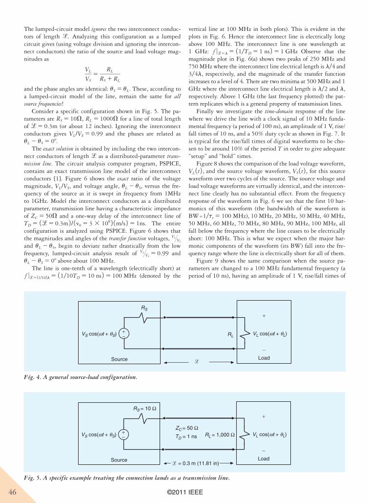
III. An ExampleConsider the typical source-load circuit shown in Fig. 4. A single-frequency, sinusoidal source, VS 1 t 2 5 VS cos 1vt 1 uS 2 , having a source resistance RS sends a signal to a load repre-sented by a load resistance RL. The source and load are sepa-rated by a parallel pair of wires or a pair of lands of length l.
TABLE 1. FREQUENCIES OF SINUSOIDAL WAVES IN FREE SPACE (AIR) AND THEIR CORRESPONDING WAVELENGTHS
The lumped-circuit model ignores the two interconnect conduc-tors of length l. Analyzing this configuration as a lumped circuit gives (using voltage division and ignoring the intercon-nect conductors) the ratio of the source and load voltage mag-nitudes as
VL
VS
5RL
RS 1 RL
and the phase angles are identical: uS 5 uL. These, according to a lumped-circuit model of the line, remain the same for all source frequencies!
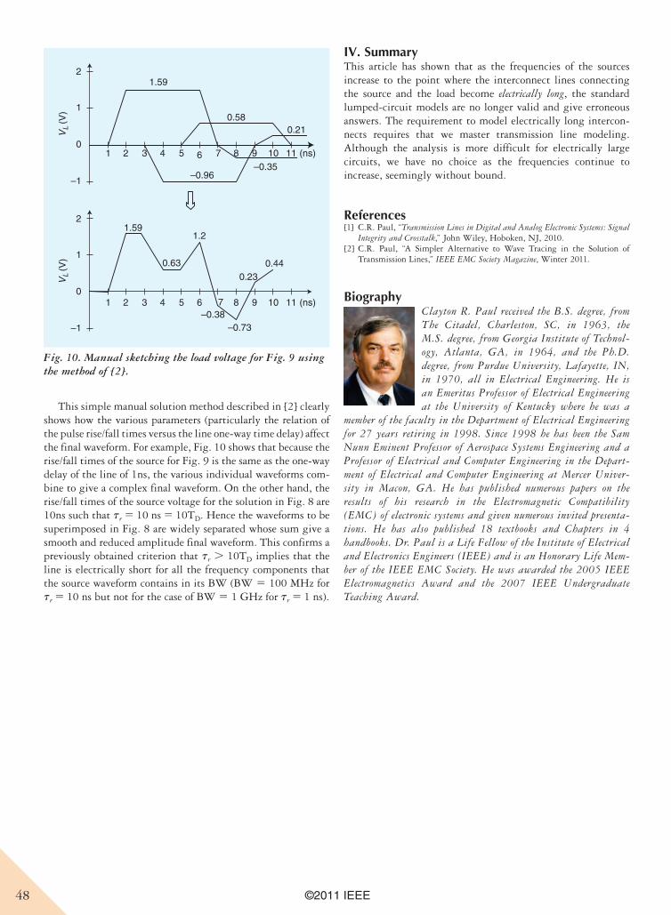
Consider a specific configuration shown in Fig. 5. The pa-rameters are RS 5 10V, RL 5 1000V for a line of total length of l5 0.3m (or about 12 inches). Ignoring the interconnect conductors gives VL/VS 5 0.99 and the phases are related as uL 2 uS 5 0o.
The exact solution is obtained by including the two intercon-nect conductors of length l as a distributed-parameter trans-mission line. The circuit analysis computer program, PSPICE, contains an exact transmission line model of the interconnect conductors [1]. Figure 6 shows the exact ratio of the voltage magnitude, VL/VS, and voltage angle, uL 2 uS, versus the fre-quency of the source as it is swept in frequency from 1MHz to 1GHz. Model the interconnect conductors as a distributed parameter, transmission line having a characteristic impedance of ZC 5 50V and a one-way delay of the interconnect line of TD 5 1l5 0.3m 2 / 1v0 5 3 3 108 2 1m/s 2 5 1ns. The entire configuration is analyzed using PSPICE. Figure 6 shows that the magnitudes and angles of the transfer function voltages, VL@VS
and uL 2 uS, begin to deviate rather drastically from the low frequency, lumped-circuit analysis result of VL@VS
5 0.99 and uL 2 uS 5 0o above about 100 MHz.
The line is one-tenth of a wavelength (electrically short) at f 0l5 11/102l 5 11/10TD 5 10 ns 2 5 100 MHz (denoted by the
vertical line at 100 MHz in both plots). This is evident in the plots in Fig. 6. Hence the interconnect line is electrically long above 100 MHz. The interconnect line is one wavelength at 1 GHz: f 0l5l 5 11/TD 5 1 ns 2 5 1 GHz Observe that the magnitude plot in Fig. 6(a) shows two peaks of 250 MHz and 750 MHz where the interconnect line electrical length is l/4 and 3/4l, respectively, and the magnitude of the transfer function increases to a level of 4. There are two minima at 500 MHz and 1 GHz where the interconnect line electrical length is l/2 and l, respectively. Above 1 GHz (the last frequency plotted) the pat-tern replicates which is a general property of transmission lines.
Finally we investigate the time-domain response of the line where we drive the line with a clock signal of 10 MHz funda-mental frequency (a period of 100 ns), an amplitude of 1 V, rise/fall times of 10 ns, and a 50% duty cycle as shown in Fig. 7. It is typical for the rise/fall times of digital waveforms to be cho-sen to be around 10% of the period T in order to give adequate “setup” and “hold” times.
Figure 8 shows the comparison of the load voltage waveform, VL 1 t 2 , and the source voltage waveform, VS 1 t 2 , for this source waveform over two cycles of the source. The source voltage and load voltage waveforms are virtually identical, and the intercon-nect line clearly has no substantial effect. From the frequency response of the waveform in Fig. 6 we see that the first 10 har-monics of this waveform (the bandwidth of the waveform is BW=1/tr 5 100 MHz), 10 MHz, 20 MHz, 30 MHz, 40 MHz, 50 MHz, 60 MHz, 70 MHz, 80 MHz, 90 MHz, 100 MHz, all fall below the frequency where the line ceases to be electrically short: 100 MHz. This is what we expect when the major har-monic components of the waveform (its BW) fall into the fre-quency range where the line is electrically short for all of them.
Figure 9 shows the same comparison when the source pa-rameters are changed to a 100 MHz fundamental frequency (a period of 10 ns), having an amplitude of 1 V, rise/fall times of
Source Load
RS
RLVS cos(ωt + θS) VL cos(ωt + θL)+−
−
+
l
Fig. 4. A general source-load configuration.
Source Load
RS = 10 Ω
RL = 1,000 ΩZC = 50 Ω
VS cos(ωt + θS) VL cos(ωt + θL)+−
−
+
TD = 1 ns
l = 0.3 m (11.81 in)
Fig. 5. A specific example treating the connection lands as a transmission line.
1ns, and a 50% duty cycle. From Fig. 6, this waveform contains the first 10 harmonics that constitute the major components in its bandwidth (BW=1/tr 5 1 GHz): 100 MHz, 200 MHz, 300 MHz, 400 MHz, 500 MHz, 600 MHz, 700 MHz, 800 MHz, 900 MHz, 1 GHz. The line length is l/10 at the fundamental frequency of it, 100 MHz, and 1l at its tenth har-monic of 1 GHz. Observe that the load voltage waveform bears no resemblance to the source waveform. From the frequency-response of the system in Fig. 6, we see that all of these har-monics fall in the frequency range where the interconnect line is electrically long (>100 MHz) so this is expected.
The plots in Figure 8 and 9 were both plotted using PSPICE. The load voltages, VL 1 t 2 , can be manually plotted using the simple method described in [2]. This solution for the VS 1 t 2 for the waveform of Fig. 9 is shown in Fig. 10 as the superposition of the scaled and delayed versions of VS 1 t 2 . This shows how the final waveform is composed of the sum of the scaled and delayed VS 1 t 2 as [2]:
VL 1 t 25 ZC
ZS1ZC
111GL2 SVS1t2TD21 1GSGL 2 VS 1t 23TD211GSGL2 2 VS 1 t 25TD21 1GSGL 2 3 VS 1 t 27TD21cT
5 1.59 VS1t21 ns220.96 VS1t23 ns210.58 VS 1t25 ns22 0.35 VS 1 t 2 7 ns2 1 0.21 VS 1 t 2 9 ns21c
where ZC/ 1ZS 1 ZC 2 11 1 GL 2 5 1.59 and 1GSGL 2 5 2 0.6 and the source and load reflection coefficients are GS 5 1RS 2 ZC 2/ 1RS 1 ZC2520.667 and GL 5 1RL2ZC2 / 1RL 1ZC2 5 0.905.
100 101 102 1030
1
2
3
4
Frequency (MHz)
100 101 102 103
Frequency (MHz)
(a)
(b)
Mag
nitu
deMagnitude of Transfer Function, VL/VS
–200
–100
0
100
200
Ang
le (
degr
ees)
Angle of Transfer Function, VL/VS
Fig. 6. Frequency response of the line in Fig. 5.
0 50 100 150 200–0.2
0
0.2
0.4
0.6
0.8
1
1.2
Time (ns)
Sou
rce
and
Load
Vol
tage
s (V
)
Two Cycles of theLoad Voltage Versus the Source Voltage
Fig. 8. Comparison of the source and load waveforms for a 1 V, 10 MHz waveform with rise/fall times of tr 5 tf 5 10 ns and a 50% duty cycle (see Fig. 7).
Fig. 7. The source voltage.
t
1V
VS(t )
10ns 100ns (10MHz)50ns 60ns
Fig. 9. Comparison of the source and load waveforms for a 1 V, 100 MHz waveform with rise/fall times of tr 5 tf 5 1 ns and a 50% duty cycle.
This simple manual solution method described in [2] clearly shows how the various parameters (particularly the relation of the pulse rise/fall times versus the line one-way time delay) affect the final waveform. For example, Fig. 10 shows that because the rise/fall times of the source for Fig. 9 is the same as the one-way delay of the line of 1ns, the various individual waveforms com-bine to give a complex final waveform. On the other hand, the rise/fall times of the source voltage for the solution in Fig. 8 are 10ns such that tr 5 10 ns 5 10TD. Hence the waveforms to be superimposed in Fig. 8 are widely separated whose sum give a smooth and reduced amplitude final waveform. This confirms a previously obtained criterion that tr . 10TD implies that the line is electrically short for all the frequency components that the source waveform contains in its BW (BW 5 100 MHz for tr 5 10 ns but not for the case of BW 5 1 GHz for tr 5 1 ns).
IV. SummaryThis article has shown that as the frequencies of the sources increase to the point where the interconnect lines connecting the source and the load become electrically long, the standard lumped-circuit models are no longer valid and give erroneous answers. The requirement to model electrically long intercon-nects requires that we master transmission line modeling. Although the analysis is more difficult for electrically large circuits, we have no choice as the frequencies continue to increase, seemingly without bound.
References[1] C.R. Paul, “Transmission Lines in Digital and Analog Electronic Systems: Signal
Integrity and Crosstalk,” John Wiley, Hoboken, NJ, 2010.[2] C.R. Paul, “A Simpler Alternative to Wave Tracing in the Solution of
Transmission Lines,” IEEE EMC Society Magazine, Winter 2011.
BiographyClayton R. Paul received the B.S. degree, from The Citadel, Charleston, SC, in 1963, the M.S. degree, from Georgia Institute of Technol-ogy, Atlanta, GA, in 1964, and the Ph.D. degree, from Purdue University, Lafayette, IN, in 1970, all in Electrical Engineering. He is an Emeritus Professor of Electrical Engineering at the University of Kentucky where he was a
member of the faculty in the Department of Electrical Engineering for 27 years retiring in 1998. Since 1998 he has been the Sam Nunn Eminent Professor of Aerospace Systems Engineering and a Professor of Electrical and Computer Engineering in the Depart-ment of Electrical and Computer Engineering at Mercer Univer-sity in Macon, GA. He has published numerous papers on the results of his research in the Electromagnetic Compatibility (EMC) of electronic systems and given numerous invited presenta-tions. He has also published 18 textbooks and Chapters in 4 handbooks. Dr. Paul is a Life Fellow of the Institute of Electrical and Electronics Engineers (IEEE) and is an Honorary Life Mem-ber of the IEEE EMC Society. He was awarded the 2005 IEEE Electromagnetics Award and the 2007 IEEE Undergraduate Teaching Award.
1 2 3 4 5 6 7 8 9 10 11 (ns)
1 2 3 4 5 6 7 8 9 10 11 (ns)
VL
(V)
2
–1
0
1
VL
(V)
2
–1
0
1
1.59
1.59
0.580.21
–0.35–0.96
1.2
0.230.44
–0.38–0.73
0.63
Fig. 10. Manual sketching the load voltage for Fig. 9 using the method of [2].
A Simple Causality Checker and Its Use in Verifying, Enhancing, and Depopulating Tabulated Data from Electromagnetic SimulationBrian Young and Amarjit S. Bhandal, ASIC Package Design Texas Instruments, Austin, TX, USA; Northampton, UK, [email protected]; [email protected]
IntroductionElectromagnetic (EM) simulators are very powerful, flexible, and accurate. They are also necessarily somewhat complex to setup, requiring user inputs on materials and material models, ports, boundary conditions, meshing frequencies, bandwidth, convergence tolerance, and other required and optional vari-ables. The simulators are in use by the full spectrum of engi-neers, from new college graduates with little formal EM training to highly experience engineers with advanced degrees in EM and numerical methods. Issues can range from poorly conceived setups to simple typos. All users face the same prob-lem: How do you know that the computed results are correct, reliable, and usable? In transient simulations, low quality computed results can easily result in non-causal models and simulation artifacts, such as faster-than-light signal propaga-tion [1][2][3].
For the most part, the decision on usability of computed results is based on the user’s judgment of the “quality” of the results from inspection, on whether the results match expecta-tions, and on the convergence error numbers produced by the simulator. Such an experienced-based approach needs to be aug-mented by a quantified quality check to help ensure the consis-tent development of high-quality models.
All data must be causal to be usable, and a causality check of the data is a strong test of data quality that is quantifiable. Many causality tests have been proposed and discussed [4][5][6][7]. The causality checker presented in [7] is reviewed and demonstrated here to show that a good causality checker is rela-tively simple to implement and can produce powerful observa-tions on the quality of data while guiding its enhancement.
Causality CheckerCausal data must satisfy the Hilbert Transform, so a direct calculation of the Hilbert Transform produces a check of causal-ity. Assuming that the S-parameters are split into real and imaginary parts as S 1v 2 5 U 1v 2 1 jV 1v 2 , then the Hilbert Transform is
U 1v 2 51p 3
`
2`
V 1v r 2v 2 v r
dv r1 K (1)
V 1v 2 5 21p 3
`
2`
U 1v r 2v 2 v r
dv r (2)
The integrals are defined according to the Cauchy principal value, and K is an unknown constant. The main difficulties
in executing the integration are manually extracting the singularity, extending the integration to infinity from bounded data, extrapolation to zero frequency, and determin-ing K.
A causality checker can be implemented by simply calculat-ing an estimate for U 1v 2 from the original V 1v 2 data using (1) and finding the error between the original and estimated data. Similarly, (2) can be used to estimate V 1v 2 from the original U 1v 2 . In this work, rather than view the errors of the real and imaginary parts, the magnitudes and phases are compared. In-terpretation of error plots is sometimes eased by averaging the errors over a rolling 1/220% bandwidth, and the plots using averaging are labeled with the averaging bandwidth. For multi-port data, the causality checker is applied independently to each port at a time.
The integrals can be computed using a piece-wise linear ap-proximation. To keep the implementation simple, the data is mirrored to negative frequencies, where the real part is an even function of frequency and the odd part is an odd function. The implementation is further simplified by deleting the data at zero frequency and letting the even/odd properties synthesize the data at zero. The piece-wise linear approximation is
U| 1v 2 5 mUk v 1 bUk, vk , v , vk11 (3)
V| 1v 2 5 mVk v 1 bVk, vk , v , vk11 (4)
where the slopes m and the intercepts b are calculated from the tabulated data. Inserting (3) into (2) and (4) into (1) results in a reconstruction of the original data as
U 1v 2 51pa
N21
k503
vk21
vk
mvkvr1 bvk
v 2 vrdvr1 K
11p 3
v0
2`
V 1v r 2v 2 v r
dv r11p 3
`
vN
V 1vr 2v 2 vr
dvr (5)
V 1v 2 5 21pa
N21
k503
vk21
vk
mUkvr1 bUk
v 2 v r dv r
21p 3
v0
2`
U 1v r 2v 2 v r
dv r21p 3
`
vN
U 1vr 2v 2 vr
dvr, (6)
where k 5 0 . . . N covers all tabulated discrete frequencies, both positive and negative, from smallest to largest. The gen-eral linear integration term is given by
To solve the special case where v 5 vk, the integration is per-formed for the intervals vk21 to vk 2 e and vk 1 e to vk11, then let e S 0. The result is then split over the two intervals.
The integration terms from negative infinity and to positive infinity must be approximated since the actual data does not exist. It is assumed that the data is simulated to very high fre-quencies so that simple extrapolation is sufficient. For the real part, an even function is required, and the simplest available is
a constant function matching the value at the highest available frequency. As before, the positive and negative frequency inter-vals are solved together. For V 1v 2 in (6),
3
v0
2`
U 1vr 2v 2 vr
dvr1 3
`
vN
U 1vr 2v 2 vr
dvr
> 3
2vN
2`
U 12vN 2v 2 vr
dvr1 3
`
vN
U 1vN 2v 2 vr
dvr
5 U 1vN 2 lnavN 2 v
vN 1 vb . (8)
For the imaginary part, an odd function is required, and the simplest available with a decreasing magnitude with increasing frequency is 1/v. For U 1v 2 in (5),
3
v0
2`
V 1vr 2v 2 vr
dvr1 3
`
vN
V 1vr 2v 2 vr
dvr
> 2 3
2vN
2`
V 1v N 2v N
v r 1v 2 v r 2 dv r1 3
`
vN
V 1vN 2v N
v r 1v 2 v r 2 dv r
5 V 1vN 2vN
vlnavN 2 v
vN 1 vb . (9)
The special cases when v 5 v0 and v 5 vN do not signifi-cantly enhance a causality check, so they are omitted for sim-plicity.
The constant K in (1) is determined by simply shifting in U 1v 2 amplitude so that U 1vmin 2 5 U 1vmin 2 , where vmin is the smallest positive frequency.
Test on Causal DataTo demonstrate the level of accuracy expected from the described causality checker, a set of 2-port S-parameters are generated for the causal lumped circuit shown in Fig. 1. S
21
magnitude and phase reconstructions and errors are shown in Fig. 2. The results show that the methodology is good to about a 1% error at 80% bandwidth, a level good enough for a causal-ity checker. Reconstruction errors at the bandwidth limits are normal and ignored.
Using the Causality CheckerThis section demonstrates a few modeling and extraction issues that can be clarified and/or fixed through the use of a causality
+
–
+
–
TermTerm1Num = 1Z = 50 Ω
TermTerm2Num = 2Z = 50 Ω
LL1L = 1.5 nHR =
LL2L = 0.5 nHR =
CC1C = 0.4 pF
RR1R = 1 Ω
Fig. 1. Lumped circuit for causality test.
0
–10
–20
–30
–40
–50
1e–08 1e–06 0.0001Frequency (GHz)
Mag
nitu
de o
f S(2
, 1),
dB
0.01 1 100
1e–08 1e–06 0.0001Frequency (GHz)
(a)
(b)
0.01 1 100
100
10
1
0.1
0.01
0.001
0.0001
1e–05
1e–06
5%
Err
or w
ith ±
0.2
BW
Ave
ragi
ng
3
2
1
0
–1
–2
–3
Pha
se o
f S(2
, 1),
Rad
ians
100
10
1
0.1
0.01
0.001
0.0001
1e–05
1e–06
5%
Err
or w
ith ±
0.2
BW
Ave
ragi
ng
DataReconstructionError
DataReconstructionError
DataReconstructionError
DataReconstructionError
Fig. 2. Reconstruction and error for a computed causal lumped data set.(a) magnitude and (b)phase.
checker. The examples are based on multiple 3D EM extrac-tions of an organic package differential pair or coupled pairs, where the single pair is shown in Fig. 3. In the first extraction, the vendor-supplied dielectric constant and loss tangent at a list of frequency points are used. Fig. 4(a) shows the magnitude of S
11 of one trace, where it can be readily identified that some-
thing is wrong from the unrealistic behavior above 25 GHz. The causality checker is applied to the data, with the results plotted in Fig. 4(b) showing very high reconstruction error not only at the problematic high frequencies but also at midrange frequencies where the data show no obvious problems.
The extraction is re-run with the vendor-supplied dielectric constant data augmented by an additional data point to elimi-nate the non-physical behavior above 25 GHz, and the results are shown in Fig. 5(a). The results are quite plausible, but are the data completely fixed, reliable, and usable? The causality check in Fig. 5(b) shows much improvement, but the errors are still quite high, indicating that the results are not yet good enough for use even though they appear good from visual in-spection.
It is known that small sets of tabulated dielectric constant and loss tangent data are generally incapable of supporting causal modeling. One causal dielectric model is described in [8], the Djordjevic´-Sarkar or D-S model. The 3D EM extraction is repeated with the causal D-S model, and the results are shown in Fig. 6, where just the combined data and causality check are shown. The causality error is greatly improved at all frequencies. Around 0.1 GHz, the error rises as the magnitude becomes very small, so the causality error is inconsequential. At frequencies above 30 GHz, the error increases, highlighting the fact that the data is aliased above
0
–10–5
–35–30–25–20–15
–40–45
0
–10
–5
–35
–30
–25
–20
–15
–40
–45
0.01 0.1 1Frequency (GHz)
Mag
nitu
de o
f S(1
, 1),
dB
Mag
nitu
de o
f S(1
, 1),
dB
10 100
0.01 0.1 1 10 100Frequency (GHz)
(a)
(b)
100
10
1
0.1
0.01
0.001
0.0001
1e–05
1e–06
5%
Err
or w
ith ±
0.2
BW
Ave
ragi
ngDataReconstruction
ErrorDataReconstruction
Error
Fig. 5. The package extraction from Fig. 4 is repeated with an additional data point describing the properties of the dielectrics. (a) magnitude and (b) magnitude reconstruction and reconstruction error.
Fig. 3. Package differential pair for extraction studies.
Fig. 4. 3D EM extraction of a package trace in an organic flip chip ball grid array package showing suspicious results. (a) magnitude and (b) magnitude reconstruction and reconstruction error.
40 GHz, where the linear frequency spacing increases from 10 MHz to 5 GHz steps.
Data depopulation can be systematically explored using a causality checker [9][10]. Continuing the examination of the example data set computed with the D-S dielectric model, S
31
is shown in Fig. 7 with the full data density and progressively depopulated data along with causality checks. The error pro-gressively increases with depopulation, enabling the modeler to select the smallest data set consistent with a given causality er-ror. The full data set is highly over-sampled with 10 MHz linear sampling steps, while sampling at 500 MHz intervals greatly reduces the size of the data set while maintaining the causal-ity error to about 5%. Depopulation at 1000 MHz intervals is clearly too sparse. Bandwidth can similarly be explored with a causality checker, with an example shown in Fig. 8.
A strategy for finding a minimum number of data points to model a good, wide-band interconnect is developed in [10]. To achieve a 5% causality error, the algorithm is• Calculate Dfmax 51/ 18td 2• Use 1.1 3 log frequency spacing until Df $ Dfmax
• Then switch to linear spacing using Dfmax
• Set fmax after 230 dB rolloff if causality check is used to validate data
where td is the interconnect delay, Dfmax is the high-frequency linear sampling interval, and fmax is the maximum model band-width. Applying the algorithm to depopulate the example data enables a 35X reduction in the size of the original data set, with the before-and-after results shown in Fig. 9.
0
–10
–5
–35
–30
–25
–20
–15
–40
–45
Mag
nitu
de o
f S(1
, 1),
dB
0.01 0.1 1 10 100Frequency (GHz)
100
10
1
0.1
0.01
0.001
0.0001
1e–05
1e–06
5%
Err
or w
ith ±
0.2
BW
Ave
ragi
ngDataReconstruction
ErrorDataReconstruction
Error
Fig. 6. The package extraction from Fig. 4 is repeated using the causal Djordjevic-Sarkar dielectric model.
Time-domain simulations are strongly affected by the level of causality of the interconnect data. Fig. 10 shows a differential time-domain reflectometry (TDR) simulation using the non-causal S-parameter data set from the simulations for Fig. 4 vs. the causal data set using the D-S model from Fig. 5. The trace starts at about 310 ps as indicated by the red arrow. Measure-ments and 2D EM extraction show that the impedance should be 100 V. The non-causal data causes several Ohms of error in the simulated trace impedance.
The negative impact of non-causal data is further demon-strated in Fig. 11 using the same data sets as Fig. 10 to calculate the impulse response of the interconnect including the back-plane. The non-causal data exhibits a large undershoot preced-ing the actual rise in the data and a similar overshoot before the fall. These flaws are not observed in the results using the D-S model. Note that the package models have the same bandwidth and data density and that the same backplane data is used for both impulse response calculations.
0
–10
–30
–20
–40
–50
Mag
nitu
de o
f S(3
, 1),
dB
0.01 0.1 1 10 100Frequency (GHz)
0.01 0.1 1 10 100Frequency (GHz)
100
10
1
0.1
0.01
0.001
0.0001
1e–05
1e–06
5%
Err
or
DataReconstruction
Error DataReconstruction
ErrorDataReconstruction
Error DataReconstruction
Error
Original(4,013 Points)
Depopulated(114 Points)
Fig. 9. Data depopulation using a systematic strategy based on causality checking enables a large reduction in data density with controlled increase in causality error. Note that rolling bandwidth averaging is not used in these plots.
110
105
100
95
90
85
80200 250 300 350
Time (ps)
Diff
eren
tial I
mpe
danc
e (Ω
)
400 450 500
Numerical TDR:
3D EM ExtractionPackage
Differential Pair
tr = 35 ps
100 Ω
Discrete Frequency DataDjordjevic-Sarkar ModelDiscrete Frequency DataDjordjevic-Sarkar Model
35
Fig. 10. Simulated TDR for a differential pair computed with two different models for the package materials.
1.4
1.2
1
0.8
0.6
0.4
0.2
0
–0.2
–0.40 0.2 0.4
Time (ns)
Vol
tage
(V
)
0.6 0.8 1
DiscreteFrequency DataDjordjevic-SarkarModel
Package(this work)
Backplane ChannelMeasured Data
Package(this work)
Fig. 11. SerDes channel impulse response computed for two different models for the package materials.
ConclusionThe implementation details of a simple causality checker are reviewed, and the checker is used to demonstrate that it can effectively identify flawed extraction data, weak material sets, and under-sampled data. The causality checker is used to derive an algorithm for selecting sampling rates and bandwidth for EM extractions of good interconnects, enabling a potentially large reduction in data points and run time. Improved extrac-tion data is shown to significantly improve S-parameter data, time domain modeling accuracy, and time-domain system-level channel simulations.
References[1] T. A rabi, A. Murphy, T. Sarkar, R. Harrington, and A. Djordjevic, “On
the modeling of conductor and substrate losses in multiconductor, multi-dielectric transmission line systems,” IEEE Tran. Microwave Theory and Techniques, vol. 39, pp. 1090–1097, July 1991.
[2] J. He, N . Nahman, and S. Riad, “A causal skin-effect model of microstrip lines,” MTT-S Int. Microwave Symp. Digest, pp. 865–868, 1993.
[3] S. Hall, T. Liang, H. Heck, and D. Shykind, “Modeling requirements for transmission lines in multi-gigabit systems,” Proc. Electrical Performance of Electronic Packaging, pp. 67–70, 2004.
[4] G. Anton ini, A. Orlandi, and V. Ricchiuti, “Causality check for SI data validation,” Proc. Signal Propagation on Interconnect, pp. 155–158, 2005.
[5] B. Xu, X . Zeng, J. He, and D-h. Han, “Checking causality of Intercon-nects through minimum-phase and all-pass decomposition,” Proc. High Density Microsystem Design and Packaging and Component Failure Analysis, pp. 67–69, 2006.
[6] P. Tiver io, S. Grivet-Talocia, “On checking causality of bandlimited sam-pled frequency responses,” Proc. Research in Microelectronics and Electronics, pp. 501–504, 2006.
[7] B. Young and A. Bhandal, “Causality checking and enhancement of 3D electromagnetic simulation data,” Elec. Perf. of Elec. Packaging and Systems, EPEPS 2010, pp. 81–84.
[8] A. Djordjevic, R. Biljic, V. Likar-Smiljanic, and T. Sarkar, “Wideband frequency-domain characterization of FR-4 and time-domain causality,” IEEE Tran. Electromagnetic Compat., vol. 43, pp, 662–667, Nov. 2001.
[9] J. Chung and A. Cangellaris, “Accuracy-preserving adaptive sampling of broadband electromagnetic spectra of interconnect structures,” Elec. Perf. of Elec. Packaging and Systems, EPEPS 2008, pp. 335–338.
[10] B. Young, “Bandwidth and density reduction of tabulated data using causality checking,” Elec. Design of Adv. Packaging and Systems Symp., EDAPS 2010, pp. 1–4.
BiographiesBrian Young received the BSEE from Texas A&M University in 1984, the MSEE from the University of Illinois in 1985, and the Ph.D. from the University of Texas in 1987. He taught electromagnetics and microwaves at Texas A&M University before moving to Hughes Aircraft to design microwave circuits and packaging for transmit/receive modules for phased array radar.
He then transitioned to Motorola to develop modeling, simulation and characterization techniques for digital packaging. This was followed by LVCMOS, LVDS, and HSTL IO circuit design at Motorola and Texas Instruments. In 2005, he started a new signal and power integrity group at Texas Instruments to ensure the success-ful integration of high-performance ASICs, and he now also man-ages the package design team in the ASIC product group. He was an Associate Editor for the IEEE Transactions on Advanced Packaging from 2001 to 2003. He is on the technical program committee for the IEEE Conference on Electrical Performance of Electronic Packag-ing and Systems, and he is the conference co-chair for 2011–2012. He is the author of the book “Digital Signal Integrity: Modeling and Simulation with Interconnects and Packages” and has authored or co-authored 33 papers and conference publications, and he holds eight patents. He is a registered professional engineer in the state of Texas.
Amarjit S. Bhandal graduated from the Uni-versity of Southampton in 1987; since that time, he has been in continuous employment in the electronics or automotive industries. For the last 15 years he has been with Texas Instruments where he is cur-rently a Member of Group Technical Staff. Amarjit is a specialist in the electrical analysis and design of custom packages for application specific devices.
His areas of expertise encompass the modelling and design of packaging interconnects for high speed signalling. During his career, Amarjit has published technical papers at several conferences and is also the holder of seven patent awards. EMC